Abstract
We demonstrate the production of organic bottom gate transistors with self-aligned electrodes, using only continuous roll-to-roll (R2R) techniques. The self-alignment allows accurate <5 µm layer-to-layer registration, which is usually a challenge in high-speed R2R environments as the standard registration methods are limited to the millimeter range—or, at best, to tens of µm if online cameras and automatic web control are utilized. The improved registration enables minimizing the overlap between the source/drain electrodes and the gate electrode, which is essential for minimizing the parasitic capacitance. The complete process is a combination of several techniques, including evaporation, reverse gravure, flexography, lift-off, UV exposure and development methods—all transferred to a continuous R2R pilot line. Altogether, approximately 80 meters of devices consisting of thousands of transistors were manufactured in a roll-to-roll fashion. Finally, a cost analysis is presented in order to ascertain the main costs and to predict whether the process would be feasible for the industrial production of organic transistors.
1. Introduction
Organic thin film transistors (OTFTs) are a promising candidate for low-cost flexible electronics due to their potential for low-temperature processing by printing, allowing plastic substrates and high-speed R2R processes to be used. The performance of small molecule or polymeric organic transistors has been steadily increasing, and state-of-the art mobility values for solution-processed transistors are already approaching or even exceeding 10 cm2V−1s−1 [1,2,3]. In addition to high performance, the whole process has to be scalable to industrial high-speed production. Otherwise, the potential for low cost cannot be utilized. Several examples of printed OTFTs already exist, as described in recent reviews [4,5,6]. However, fully R2R-processed transistors are still less frequently demonstrated [7,8,9,10,11,12]. The production of fully printed OTFTs faces two main challenges: resolution and registration—especially in the R2R environment. High resolution is needed for minimizing the foot print of the transistor, which is important, e.g., in flexible display applications, and for decreasing the channel length, which would lead to higher switching speeds. Traditional printing processes are limited to a resolution of a few tens of µm [13]. For smaller dimensions, special R2R-compatible methods are needed, e.g., UV-nanoimprint lithography (UV-NIL) [14] or attoliter gravure printing [15] have been demonstrated in a sheet-to-sheet (S2S) process for flexible OTFTs. Channel lengths from 10 µm down to the sub-micrometer range have been achieved with these methods.
Smaller dimensions naturally also increase the challenges in registration, which can be improved up to a certain limit with online cameras and continuous adjustment of the web. However, the high-speed R2R printing machines are not capable for µm-scale registration, which is required for small-channel transistors, and thus other methods are needed. The most demanding step in the registration of transistor layers is the alignment between the gate and source and drain electrodes. It is important to control the relative position of source and drain and gate electrodes while minimizing the overlap. The overlap between electrodes induces parasitic capacitance—one of the reasons for low switching speed [16]—and also increases the risk of short circuits. The most promising method to deposit the source, drain and gate electrodes in register is to use self-alignment. Stadlober and her group have, for instance, demonstrated a self-alignment method to pattern the channel area with the help of a UV-NIL-processed gate electrode as the photolithography mask in a bottom gate OTFT structure [14,17]. The S2S process demonstrated led to as little as a 200 nm overlap between electrodes. Also, the source and drain electrodes have been used as a photolithography mask to successfully align the gate electrode in a top gate OTFT structure [18]. In addition, e.g., a wetting-based roll-off process [19] or doping of polyaniline via UV-exposure [20] have been utilized to align source and drain electrodes with the gate.
The goal of this work was to test whether it is possible to transfer the nanoimprint lithography and self-alignment concept to a pilot scale R2R environment. The results show that the self-alignment process, using a gate electrode as a photolithography mask, can be transferred to a continuously moving R2R line with µm-scale overlap and used in fully R2R-processed transistor circuits. To be industrially viable, the OTFT process has to be cost-effective. Thus, in addition to the R2R process description, we present a cost scenario for R2R-processed transistor circuits, which gives an estimate for the production costs vs. production volume, and predicts when it is sensible to use a R2R process line or when a batch process is a better option.
2. Experimental Section
2.1. Materials
The transistors were deposited on a 30 cm wide and 125 µm thick heat-stabilized polyethylene terephthalate roll from DuPont Teijin Films (Hopewell, VA, USA). Graphical black ink from SunChemical (Espoo, Finland) was used as the printed lift-off mask, and Ag pellets for R2R evaporation were acquired from Kurt J. Lesker Company (Jefferson Hills, PA, USA). The photoresist (product ma-P1275), which was used in the self-alignment process, was provided by micro resist technology GmbH (Berlin, Germany). Photo-crosslinkable poly(methyl methacrylate) (PMMA) with a photoinitiator (product GRAPE014) and polymeric semiconductor (product GRAPE114) were received as ready solutions from BASF SE.
2.2. Process Description
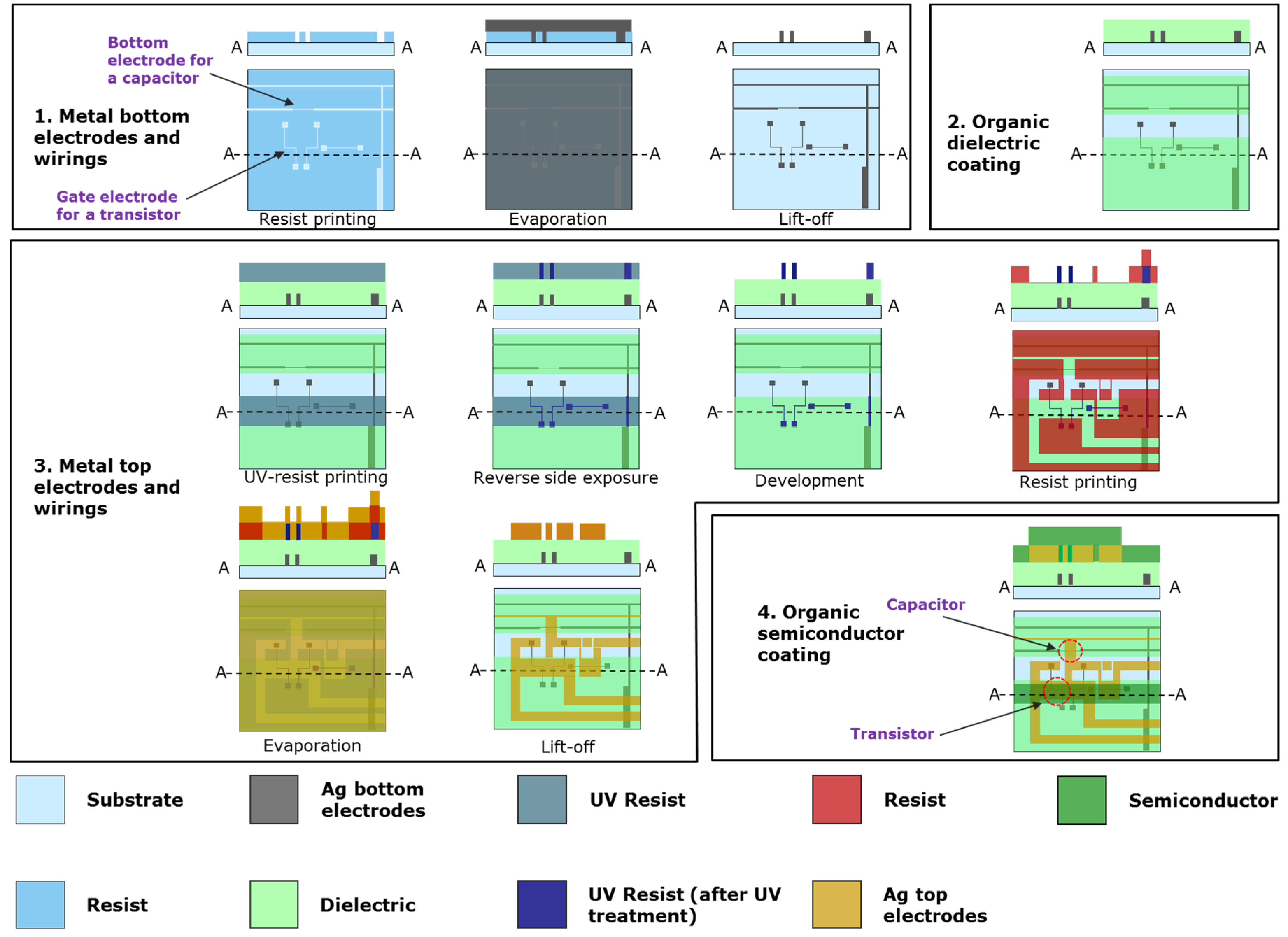
Figure 1 shows the R2R machinery that was used in the production of the transistors. All equipment consists of pilot scale devices, capable of high throughput production. The hot embossing unit, shown in the middle, was initially tested for patterning the gate electrode in high (0.5–5 µm) resolution. However, nanoimprint lithography cannot provide residual-free patterns, at least with the R2R hot embossing tools. After several test runs, it also became clear that the imprint quality was still too inhomogeneous for high-speed removal of the residual resist layers, indicating that the high-speed R2R NIL process, using a hot embossing unit, is not compatible for producing µm-scale structures on such large areas. Thus, as described below, we produced the gate electrode with direct resist printing and lift-off, which can provide patterns varying from 25 to 70 µm, and concentrated on making the self-alignment technique work in the R2R process. Figure 2 also shows a schematic of the transistor structure, including the film thickness values and production methods for each layer. In addition to the transistors, the layout consisted of wirings and capacitors, representing the components needed in the front end of a radio-frequency identification (RFID) circuit. The following methods were used for the different layers in the transistor circuits, as also shown in Figure 3:
- Bottom electrodes: The resist (graphical ink) was deposited as a patterned layer by flexographic printing with a speed of 10 m/min and 120 °C drying temperature, followed by Ag evaporation and lift-off for bottom electrode formation. The lift off process was performed in an ultrasonic bath using acetone as the solvent and a web speed of 0.3–0.5 m/min. Gate electrodes, bottom electrodes for the capacitors and wirings were manufactured in one step with a resolution varying from 25–70 µm for the gate to 1–3 mm for the wirings.
- Dielectric: The insulating PMMA layer was deposited by reverse gravure coating and subsequent drying (140 °C) and inline crosslinking with UV light with a speed of 8 m/min. The process was repeated twice in order to achieve a film thickness of approximately 800 nm for the dielectric layer.
- Top electrodes: The first resist (positive photoresist) was deposited by flexographic printing as a stripe, followed by reverse-side UV exposure through the substrate and development in a potassium hydroxide (KOH) solution for patterning the channel area. The gate was used as the photomask since the direct R2R registration is not accurate enough for such small µm-scale patterns. The speed of the photoresist printing process was 8 m/min, using a drying temperature of 140 °C. The reverse-side UV exposure step and development in KOH were performed at speeds of 10 and 2 m/min, respectively. The second resist (graphical ink) was printed by flexography with a speed of 10 m/min, and was used to pattern the rest of the top electrodes (capacitor and wirings). Here, the online registration was sufficient since the dimensions of the patterns are larger. Thus, we patterned the second resist directly in the printing process. The two resist layers were covered with a 100 nm thick Ag layer through R2R evaporation. Subsequently, a simultaneous lift-off process in acetone for both resists (UV-exposed photoresist and graphical ink) was used to finalize the metallization of the source and drain electrodes, top electrodes for the capacitors and the wirings.
- Semiconductor: The polymeric semiconductor was deposited by reverse gravure coating on top of the transistor structures with a speed of 4 m/min, using a drying temperature of 90 °C. The process was repeated three times in order to achieve a film thickness of 60 nm.
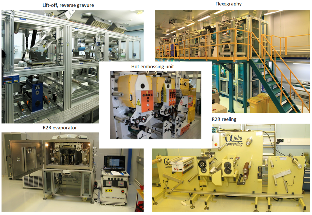
Figure 1.
Pilot scale machinery used in the processing.
Figure 1.
Pilot scale machinery used in the processing.

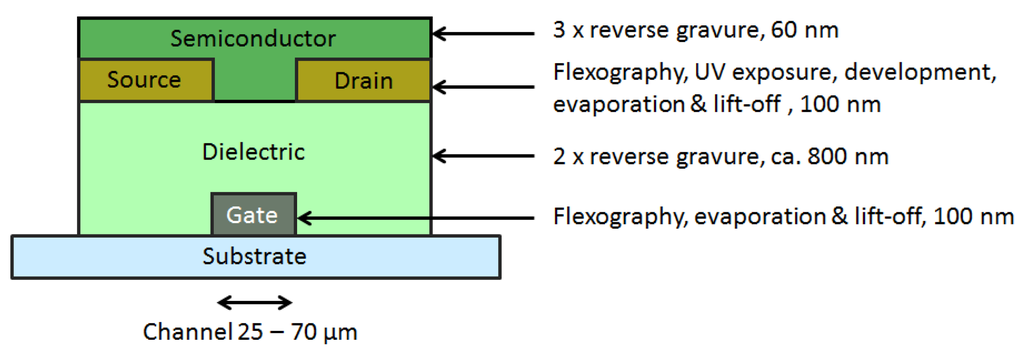
Figure 2.
Schematic of the transistor structure (not in scale), showing the deposition methods and thickness values for each layer.
Figure 2.
Schematic of the transistor structure (not in scale), showing the deposition methods and thickness values for each layer.


Figure 3.
Roll-to-roll process flow, showing the layout of each layer. The cross-section of the layers at the position marked with A is shown on top of each image. Note that the width and height of the structures in the cross-section images have been enlarged for clarity.
Figure 3.
Roll-to-roll process flow, showing the layout of each layer. The cross-section of the layers at the position marked with A is shown on top of each image. Note that the width and height of the structures in the cross-section images have been enlarged for clarity.
2.3. Characterization
The R2R-produced transistors were characterized with KEITHLEY 2636 SYSTEM SourceMeter® (Cleveland, OH, USA) in a normal laboratory atmosphere. A profilometer (Dektak 150, Veeco, Tucson, AZ, USA) was used for film thickness measurements, and the channel area was characterized in more detail with a field emission gun scanning electron microscope (FEGSEM) (Zeiss Merlin, Carl Zeiss Microscopy GmbH, Jena, Germany).
3. Results and Discussion
3.1. Printing Process and Electrical Performance
The first process step, i.e., flexographic printing of resist, Ag evaporation and lift-off, gave 25–70 µm wide gate electrodes and 1–3 mm wide wirings in one step. Even though simple one-step additive printing methods are capable of producing patterns and gaps with a resolution of 25–70 µm, we chose to use the three-step flexo printing, evaporation and lift-off process for the gate electrode due to the following reasons: (i) Directly R2R-printed metallic nanoparticle inks cannot provide as smooth and spike-free layers as evaporated metal layers, which would increase the risk of short circuits; (ii) The self-alignment process requires a completely non-transparent gate electrode layer—especially at the edge area. Electrodes, which have been prepared by evaporation and lift-off, have sharp edges and the Ag thickness does not decrease at the edge area. Printed metallic nanoparticle inks were considered to have more risk for semi-transparent edge areas, which would be harmful for the reverse-side UV exposure step and might cause scattering of light. (iii) Ultimately, the goal is to decrease the channel length below 25 µm with the help of nanoimprinting techniques. The flexo printing, evaporation and lift-off process is the closest available method to mimic that process and it helps us to understand the requirements for the lift-off and self-alignment techniques.
The next step, i.e., dielectric coating and inline crosslinking with UV light, produced an 800 nm thick insulating layer in two subsequent runs. The photoresist, creating channel areas for top source and drain electrodes, was flexographically printed and patterned by using the gate electrodes as the photomask with UV exposure through the substrate with a special reverse-side exposure setup built in the printing line. The footprint of source and drain electrodes and wirings for the electrodes were patterned similarly to the bottom electrodes. The results showed that it was possible to use two different resists in one lift-off step, since both of the resists could be removed in a single evaporation and lift-off step in acetone, giving continuous Ag patterns.
Finally, the reverse gravure coating for the semiconductor resulted in a continuous layer on the channel area, finalizing the bottom gate transistor structures. The selected ink and engravings (7.8 mL/m2) produced as low as 20 nm layer thickness in one printing run, which is too low for reliable transistor operation. In this work, we used three coating cycles to overcome the problem and to achieve a 60 nm thick semiconducting layer. Thus, if reverse gravure coating is to be used in future work, the suggestion is to use a higher volume in the cylinder, which would allow achieving the required film thickness with one coating step. However, another option would be to print the semiconducting layer with forward gravure, as the GRAPE114 semiconducting polymer ink can be successfully R2R-printed with the standard forward gravure printing technique in just one step [8]. Reverse gravure coating was selected for this process, since one of the goals was to study whether the reverse gravure technique is also suitable for transistor applications. Reverse gravure coating is not as sensitive to the rheology of the ink as forward gravure printing, which would also allow more challenging inks to be deposited in a R2R process. Thus, the benefit of using reverse gravure printing would be the ability to choose the formulation more freely, while forward gravure printing often requires careful optimization of the ink and the engravings. However, reverse gravure is a coating technique, i.e., it cannot produce patterned structures, which are needed for high-performance transistors. Thus, forward gravure (or another printing technique) is the recommended method for the semiconducting layer, if the ink rheology allows. Nevertheless, reverse gravure coating remains an option for challenging inks.
Figure 4a shows a photograph of one repeat unit of the roll, which contains four transistor circuits with the same layout but different channel lengths, i.e., 25, 40, 60 and 70 µm. Each quarter contains three transistors (marked in the photograph with black squares), wirings and capacitors. Two types of registration marks were used to control the registration both in the machine and cross direction during the run. The gate electrode is too small to be visible in the photograph and thus we used SEM to study the channel area in more detail. The SEM image in Figure 4b shows that the source and drain electrodes are self-aligned with the gate electrode, and the overlap between the electrodes is approximately 2 µm, as shown with the brighter color where the two 100 nm thick Ag electrode layers are on top of each other.
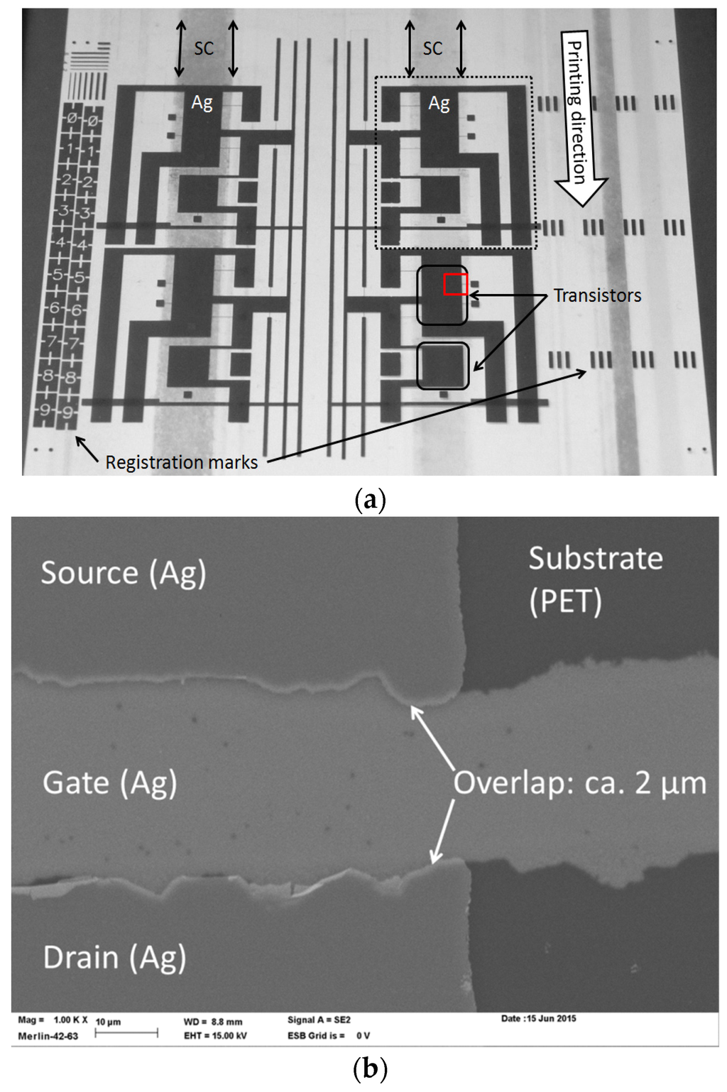
Figure 4.
(a) Photograph of the roll-to-roll–fabricated thin film transistor circuits, containing four different quarters (marked with a dotted line), each having a different transistor channel length. The positions of the semiconductor layer (SC), Ag electrodes, transistors and registration marks are marked in the image; (b) The scanning electron microscope (SEM) image shows a magnification of the channel area from the position marked with the red square. Scale bar in the SEM image is 10 µm.

The channel dimensions and yield values for complete transistors are collected in Table 1, which shows that the yield improves when the channel length increases. The sampling size of the mapping was 24 units, containing 24 individual transistors in all quarters. The stacking of different layers, i.e., registration, which generally causes loss of yield, was overcome with the self-alignment concept and flexible design, and it did not lead to any failures in the devices. The failure mechanisms of TFTs were purely short circuits and leakages between source and drain and between gate and source/drain electrodes. The data shows that with this transistor structure, the 25 µm sized gate was too narrow for a reliable R2R process: even though parts of the 25 µm channel structures were patterned successfully (as seen in the SEM image in Figure 4b), all of the complete transistors were nonfunctional in this quarter, i.e., the process was not consistent in the large, approximately 12 mm wide channels. Most of these structures were short-circuited between the source and drain electrodes, which means that the flexo printing, evaporation and lift-off step for the gate did not produce continuous lines or the lift-off process for the source and drain electrodes was not reliable for narrow gaps. For longer channels (60–70 µm), the process works better with approximately 65% yield. With these channel lengths, approximately 80% of the nonfunctional transistors still had problems with source and drain electrodes and the rest were leaking between the gate and source/drain. One of the ways to improve the self-alignment process would be minimizing the dielectric thickness, which would lead to decreased scattering of light during the reverse-side UV-exposure through the dielectric. However, based on SEM images (as in Figure 4b), scattering is not the main problem and it becomes important only if channel length decreases below 5 µm. Thus, the best way to improve the yield would be to concentrate on the gate process to guarantee continuous narrow lines, and, in addition, focus on the source/drain lift-off step in order to find optimal lift-off solvent and resist combinations for the process. Despite the limitations with the short channel lengths, demonstration of the self-alignment concept of metallic electrodes in a continuous R2R process is already a significant improvement and a step towards high throughput, large-scale production of flexible OTFTs.

Table 1.
Channel dimensions of the roll-to-roll–processed devices and yield of the final transistors for each quarter.
| Area | Channel Length (µm) | Channel Width (µm) | W/L Ratio | Yield (%) |
|---|---|---|---|---|
| Quarter 1 | 70 | 12,180 | 175 | 67 |
| Quarter 2 | 60 | 12,140 | 200 | 63 |
| Quarter 3 | 40 | 12,180 | 305 | 38 |
| Quarter 4 | 25 | 12,220 | 490 | 0 |
| All | - | - | - | 42 |
A summary of the electrical characteristics for transistors with the 70 µm channel length is given in Table 2. The mobility achieved is moderate, partly due to the uncovered semiconductor layer, which is constantly exposed to air, and partly due to the usage of Ag as the electrode material, which is known to cause significant contact resistance. Similar material combinations have previously shown mobility of approximately 0.02 cm2/(Vs) in R2R-processed top gate transistors with Ag electrodes, where the semiconductor was protected from air exposure by the dielectric [8]. However, these results show that the self-alignment concept can produce working transistors when transferred to a continuous R2R process environment, which is an important demonstration of feasibility of R2R processes for µm-scale registration.

Table 2.
Electrical characteristics of transistors with a channel length of 70 µm and a width of 12,180 µm. The columns show the mean, standard deviation (std), minimum (min) and maximum (max) value for each measured parameter.
| Statistical Value | Drain Current (A) | Mobility (cm2/(Vs)) | On/Off-Ratio | Subthreshold Slope (V) | Turn-on Voltage (V) |
|---|---|---|---|---|---|
| mean | 6.5 × 10⁻⁸ | 1.6 × 10⁻³ | 1300 | 0.89 | −2.1 |
| std | 7.3 × 10⁻⁸ | 1.6 × 10⁻³ | 1400 | 0.48 | 1.2 |
| min | 2.9 × 10⁻⁹ | 8.8 × 10⁻⁵ | 200 | 0.41 | −4.3 |
| max | 2.7 × 10⁻⁷ | 5.3 × 10⁻³ | 5100 | 2.10 | −0.1 |
3.2. Cost Analysis
The information about materials, tooling (printing cylinders, etc.) and energy consumption during the printing runs, as well as investment, facility and labor costs, was used to prepare a cost analysis for R2R production of imaginary 5 cm × 5 cm sized flexible transistor circuits, each containing a few hundred transistors. This circuit structure represents a level of complexity comparable to that of an RFID tag. It should, however, be noted that the performance and size of the transistors presented here is not yet sufficient for realization of circuits having hundreds of transistors and the process was used just as a model for estimating the production costs.
The web speed in this assessment was set to 5 m/min, which is a typical average value for R2R production of printed electronics. The web width in the calculations was 20 cm, while the effective width available for the circuits was 15 cm. These widths are typical of research or pilot-scale production facilities, whereas in actual production the web width can easily be half a meter or more. Even with the modest speed and limited web width taken with our example, up to 100,000 flexible circuits can be produced during one work shift and around 30 million can be produced annually. Having a web width of 50 cm, over 100 million flexible circuits can easily be produced in a year.
The material costs were calculated using actual prices and amounts for the materials used. However, for the semiconductor we used an estimated price of 422 €/g, which corresponds to the cost of poly(3-hexylthiophene-2,5-diyl), representing a widely used commercially available polymeric p-type semiconductor material. An average of 84% of solvent recycling was assumed. In addition, recovery of excess Ag from the evaporation chamber was assumed. The results are summarized in Figure 5, which shows the total production costs (€/piece) as a function of annual production volume. In addition, the cost structure is opened for two cases, i.e., for a production volume of 500,000 or five million circuits/year. The graph shows that the most important cost driver is the production volume. With low production volumes—below 100,000 pieces annually—the total production costs per piece are very high and dominated by the fixed costs. To be economically viable, the production volumes need to be up-scaled to hundreds of thousands or millions in order to minimize the contribution of fixed costs. Thus, the analysis suggests that a S2S batch process is preferred for annual production volumes of 100,000–200,000 or less.
The material costs dominate when the production volume reaches one million pieces/year or more. For a five million annual production volume, the costs are ~0.42 €/piece, where 72% of the costs (0.3 €/piece) are due to materials. With current prices and using recycling of Ag, the material costs are highly dependent on the semiconductor price, which represents 85% of the total material costs (0.26 €/piece). As the semiconductor price is seen to decrease for large production volumes, it is possible to reduce the total costs below 0.20 €/piece in the future, using an estimated price of 42 €/g for the semiconductor (one-tenth of the current price). The fixed costs for a five million annual production are estimated to be 0.12 €/piece, which sets the lowest limit for the flexible circuit price.
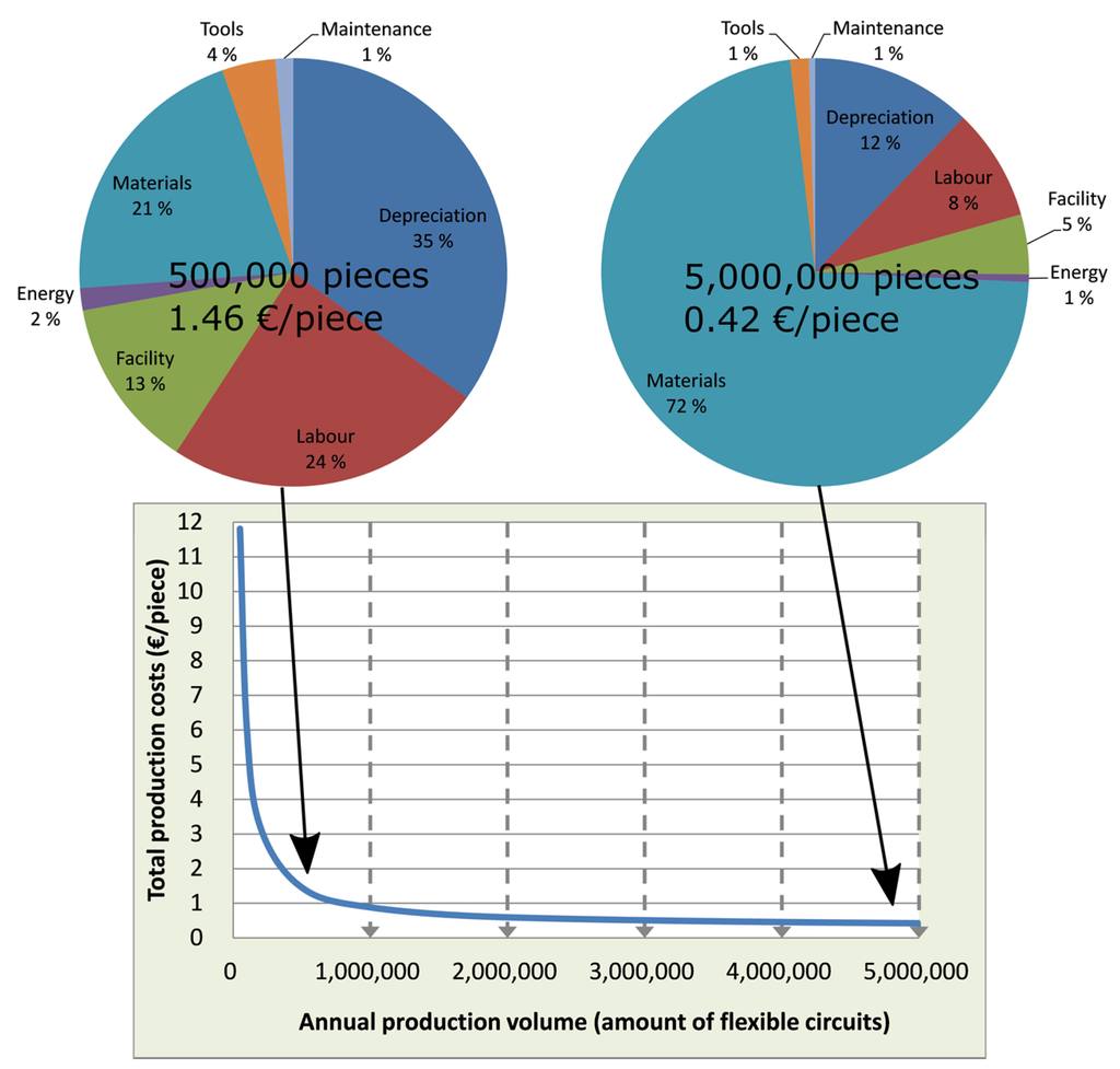
Figure 5.
Share of the different cost items in the cost-of-production analysis for an annual production of 500,000 or five million flexible circuits fabricated with the current R2R fabrication technology and the relation of total production costs to production volume.
Figure 5.
Share of the different cost items in the cost-of-production analysis for an annual production of 500,000 or five million flexible circuits fabricated with the current R2R fabrication technology and the relation of total production costs to production volume.

4. Conclusions
We have shown that the self-alignment process, which uses a metallic gate electrode as a photolithography mask, can be transferred to a continuous R2R process. Currently, with an 800 nm thick dielectric layer, the R2R process leads to as low as 2 µm overlap for the gate and source/drain electrodes and shows one solution to overcome the registration limitations in a R2R line. Self-alignment is especially important in transistors since the channel area is small and the printing machines are not capable of such accurate µm-scale registration. The functionality of the electrodes and the self-alignment concept was demonstrated in fully R2R-processed organic transistors.
In addition to the transistors, the printing layout consisted of capacitors and wirings, which helped us to understand the challenges in R2R production of transistor circuits. This information was used to prepare a cost analysis for the production of transistor circuits with a level of complexity similar to an RFID tag. The cost analysis showed that R2R production of organic transistor circuits becomes profitable only with large production volumes, i.e., more than one million pieces/year. In the case of five million pieces/year, the cost for one flexible circuit is 0.42 € where 72% of the costs come from the materials. With high production volumes and current material pricing, the main cost driver is the semiconductor, which covers 85% of the material costs with an estimated price of ca. 400 €/g. With large production volumes, the material costs will also decrease, resulting in prices below 0.20 €/piece.
Acknowledgments
The authors acknowledge European Project Printable, organic and large-area realisation of integrated circuits POLARIC (FP7-247978) for funding. Asko Sneck is acknowledged for taking the SEM image and Tomi Hassinen for helping with the OTFT analysis.
Author Contributions
All authors contributed to the planning of experiments. In addition, Marja Vilkman wrote the manuscript, Teemu Ruotsalainen designed the circuit and analyzed the transistor data, Kimmo Solehmainen prepared the cost analysis, and Elina Jansson and Johanna Hiitola-Keinänen performed the R2R runs. The process flow was designed by Teemu Ruotsalainen, Elina Jansson and Johanna Hiitola-Keinänen.
Conflicts of Interest
The authors declare no conflict of interest.
References
- Minemawari, H.; Yamada, T.; Matsui, H.; Tsutsumi, J.; Haas, S.; Chiba, R.; Kumai, R.; Hasegawa, T. Inkjet printing of single-crystal films. Nature 2011, 475, 364–367. [Google Scholar] [CrossRef] [PubMed]
- Hamaguchi, A.; Negishi, T.; Kimura, Y.; Ikeda, Y.; Takimiya, K.; Bisri, S.Z.; Iwasa, Y.; Shiro, T. Single-Crystal-Like Organic Thin-Film Transistors Fabricated from Dinaphtho[2,3-b:2′,3′-f]thieno[3,2-b]thiophene (DNTT) Precursor-Polystyrene Blends. Adv. Mater. 2015, 27, 6606–6611. [Google Scholar] [CrossRef] [PubMed]
- Shi, S.; Shi, K.; Yu, G.; Li, X.; Wang, H. Naphtho[1,2b;5,6b′]difuran-based donor–acceptor polymers for high performance organic field-effect transistors. RSC Adv. 2015, 5, 70319–70322. [Google Scholar] [CrossRef]
- Kang, B.; Lee, W.H.; Cho, K. Recent advances in organic transistor printing processes. ACS Appl. Mater. Interfaces 2013, 5, 2302–2315. [Google Scholar] [CrossRef] [PubMed]
- Xu, Y.; Liu, C.; Khim, D.; Noh, Y.-Y. Development of high-performance printed organic field-effect transistors and integrated circuits. Phys. Chem. Chem. Phys. 2015, 17, 26553–26574. [Google Scholar] [CrossRef] [PubMed]
- Mandal, S.; Noh, Y.-Y. Printed organic thin-film transistor-based integrated circuits. Semicond. Sci. Technol. 2015, 30, 064003. [Google Scholar] [CrossRef]
- Koo, H.; Lee, W.; Choi, Y.; Sun, J.; Bak, J.; Noh, J.; Subramanian, V.; Azuma, Y.; Majima, Y.; Cho, G. Scalability of carbon-nanotube-based thin film transistors for flexible electronic devices manufactured using an all roll-to-roll gravure printing system. Sci. Rep. 2015, 5, 14459. [Google Scholar] [CrossRef] [PubMed]
- Vilkman, M.; Hassinen, T.; Keränen, M.; Pretot, R.; van der Schaaf, P.; Ruotsalainen, T.; Sandberg, H.G.O. Fully roll-to-roll processed organic top gate transistors using a printable etchant for bottom electrode patterning. Org. Electron. 2015, 20, 8–14. [Google Scholar] [CrossRef]
- Bollström, R.; Tobjörk, D.; Dolietis, P.; Salminen, P.; Preston, J.; Österbacka, R.; Toivakka, M. Printability of functional inks on multilayer curtain coated paper. Chem. Eng. Process. 2013, 68, 13–20. [Google Scholar] [CrossRef]
- Hambsch, M.; Reuter, K.; Stanel, M.; Schmidt, G.; Kempa, H.; Fügmann, U.; Hahn, U.; Hübler, A.C. Uniformity of fully gravure printed organic field-effect transistors. Mater. Sci. Eng. B 2010, 170, 93–98. [Google Scholar] [CrossRef]
- Huebler, A.C.; Doetz, F.; Kempa, H.; Katz, H.E.; Bartzsch, M.; Brandt, N.; Hennig, I.; Fuegmann, U.; Vaidyanathan, S.; Granstrom, J.; et al. Ring oscillator fabricated completely by means of mass-printing technologies. Org. Electron. Phys. Mater. Appl. 2007, 8, 480–486. [Google Scholar] [CrossRef]
- Jung, M.; Kim, J.; Noh, J.; Lim, N.; Lim, C.; Lee, G.; Kim, J.; Kang, H.; Jung, K.; Leonard, A.D.; et al. All-printed and roll-to-roll-printable 13.56-MHz-operated 1-bit RF tag on plastic foils. IEEE Trans. Electron Devices 2010, 57, 571–580. [Google Scholar] [CrossRef]
- Moonen, P.F.; Yakimets, I.; Huskens, J. Fabrication of transistors on flexible substrates: From mass-printing to high-resolution alternative lithography strategies. Adv. Mater. 2012, 24, 5526–5541. [Google Scholar] [CrossRef] [PubMed]
- Gold, H.; Haase, A.; Fian, A.; Prietl, C.; Striedinger, B.; Zanella, F.; Marjanović, N.; Ferrini, R.; Ring, J.; Lee, K.-D.; et al. Self-aligned flexible organic thin-film transistors with gates patterned by nano-imprint lithography. Org. Electron. 2015, 22, 140–146. [Google Scholar] [CrossRef]
- Kang, H.; Kitsomboonloha, R.; Ulmer, K.; Stecker, L.; Grau, G.; Jang, J.; Subramanian, V. Megahertz-class printed high mobility organic thin-film transistors and inverters on plastic using attoliter-scale high-speed gravure-printed sub-5μm gate electrodes. Org. Electron. 2014, 15, 3639–3647. [Google Scholar] [CrossRef]
- Baeg, K.-J.; Jung, S.-W.; Khim, D.; Kim, J.; Kim, D.-Y.; Koo, J.B.; Quinn, J.R.; Facchetti, A.; You, I.-K.; Noh, Y.-Y. Low-voltage, high speed inkjet-printed flexible complementary polymer electronic circuits. Org. Electron. 2013, 14, 1407–1418. [Google Scholar] [CrossRef]
- Rothländer, T.; Fian, A.; Kraxner, J.; Grogger, W.; Gold, H.; Haase, A.; Stadlober, B. Channel length variation in self-aligned, nanoimprint lithography structured OTFTs. Org. Electron. 2014, 15, 3274–3281. [Google Scholar] [CrossRef]
- Noh, Y.; Zhao, N.I.; Caironi, M.; Sirringhaus, H. Downscaling of self-aligned, all-printed polymer thin-film transistors. Nat. Nanotechnol. 2007, 2, 784–789. [Google Scholar] [CrossRef] [PubMed]
- Tseng, H.-Y.; Subramanian, V. All inkjet-printed, fully self-aligned transistors for low-cost circuit applications. Org. Electron. 2011, 12, 249–256. [Google Scholar] [CrossRef]
- Jussila, S.; Puustinen, M.; Hassinen, T.; Olkkonen, J.; Sandberg, H.G.O.; Solehmainen, K. Self-aligned patterning method of poly(aniline) for organic field-effect transistor gate electrode. Org. Electron. 2012, 13, 1308–1314. [Google Scholar] [CrossRef]
© 2016 by the authors; licensee MDPI, Basel, Switzerland. This article is an open access article distributed under the terms and conditions of the Creative Commons by Attribution (CC-BY) license (http://creativecommons.org/licenses/by/4.0/).
