
Effect of Edge Roughness on Static Characteristics of Graphene Nanoribbon Field Effect Transistor


Abstract
:
1. Introduction
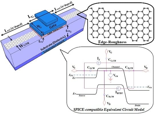
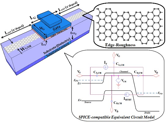
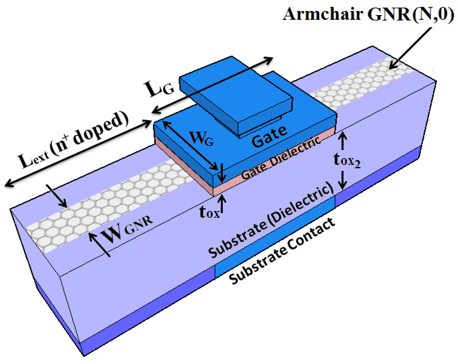
2. GNR FET Structure
3. GNR FET Model
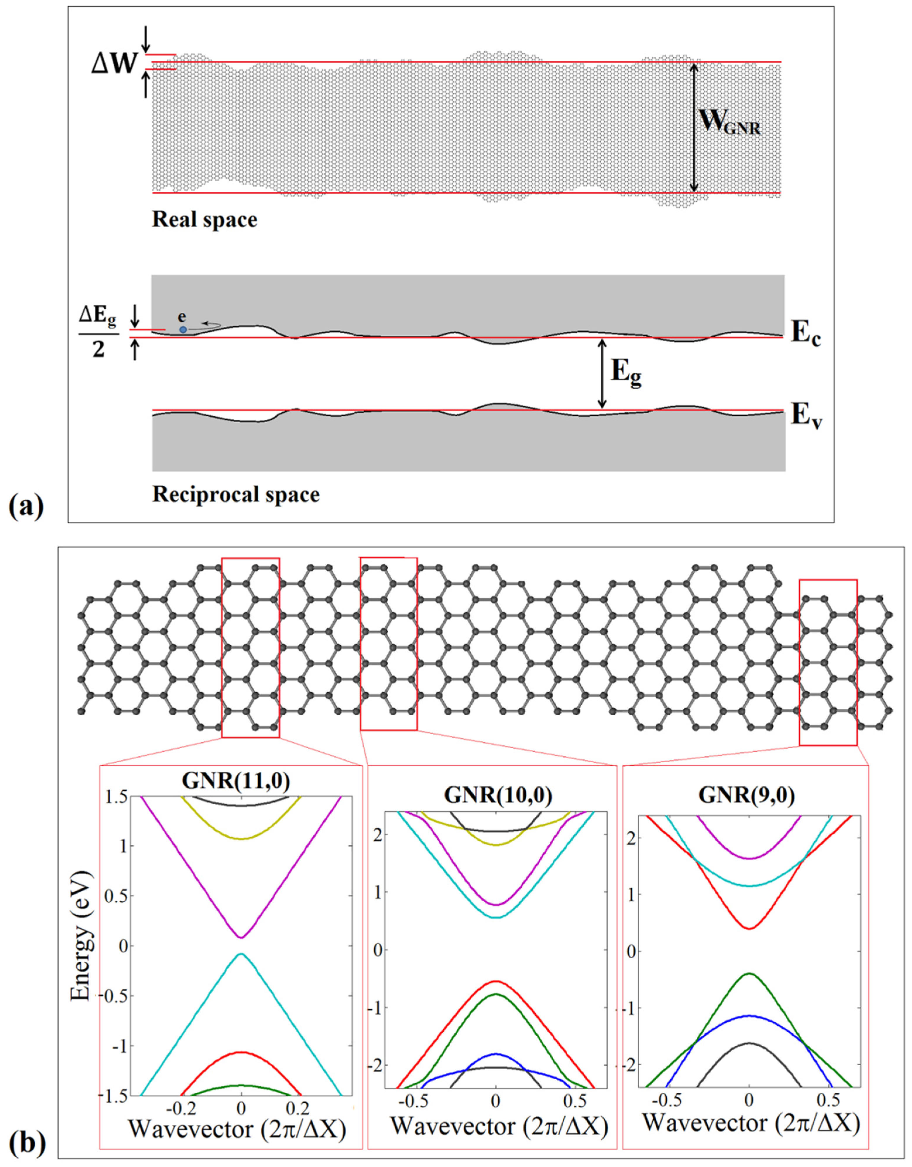
3.1. Computing GNR Subbands
3.2. Finding Channel Surface Potential
3.2.1. Computing Channel Charge
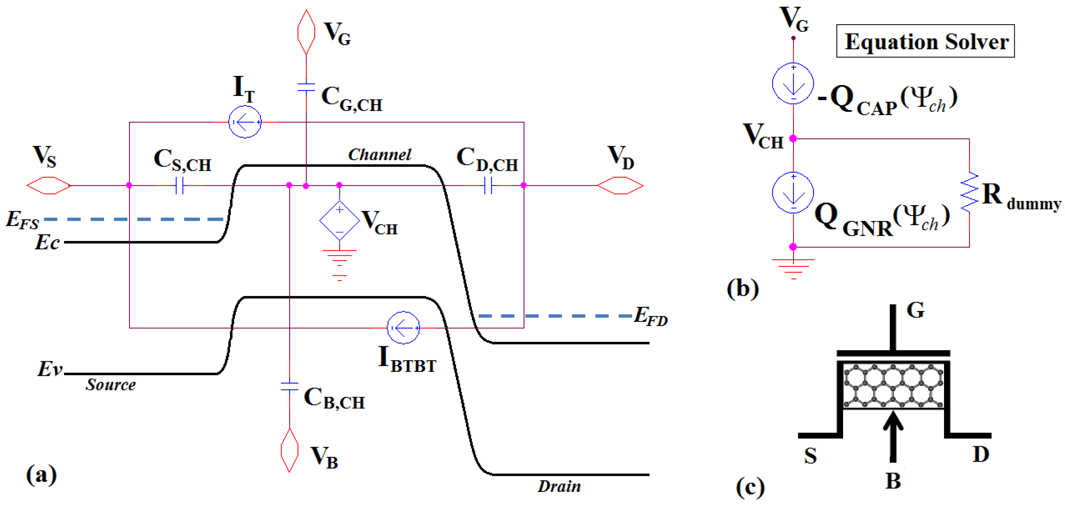
3.2.2. Computing Transient Capacitance Charge
3.3. Current Modeling
3.3.1. Computing Thermionic Current
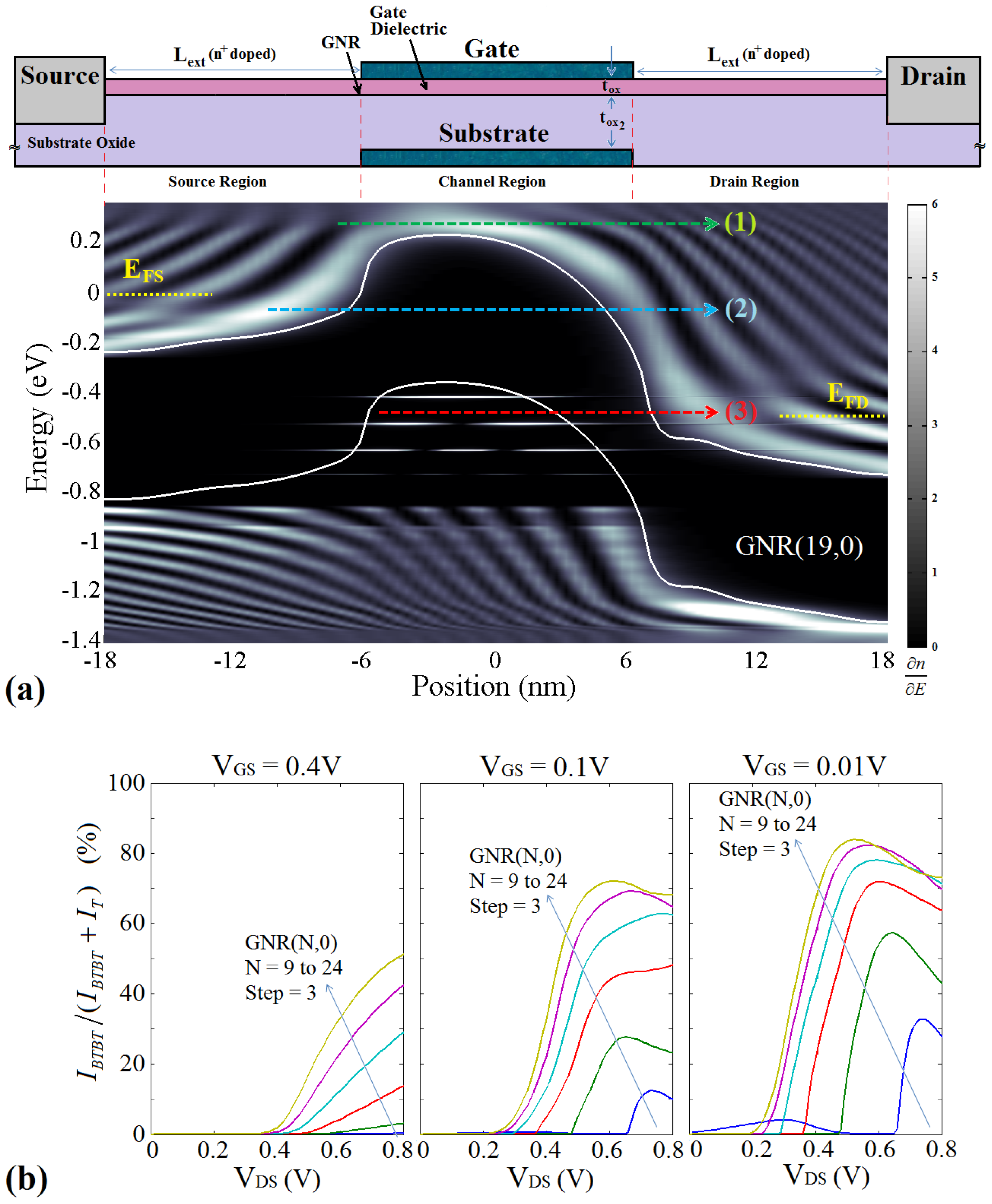
3.3.2. Evaluating Band-to-Band-Tunneling Current and Charge
3.4. Non-Ballistic Transport
3.5. Extracting Fitting Parameters
- (1)
- Obtain the numerical data from NEGF simulation for bias conditions and the device geometries related to BTBT phenomena.
- (2)
- Obtain the analytical results using the developed model for the same bias conditions and device geometries for a given fitting parameter.
- (3)
- Change a fitting parameter according to its broad range to determine the best value in which the root mean square error (RMSE) between the numerical and analytical data is minimized.
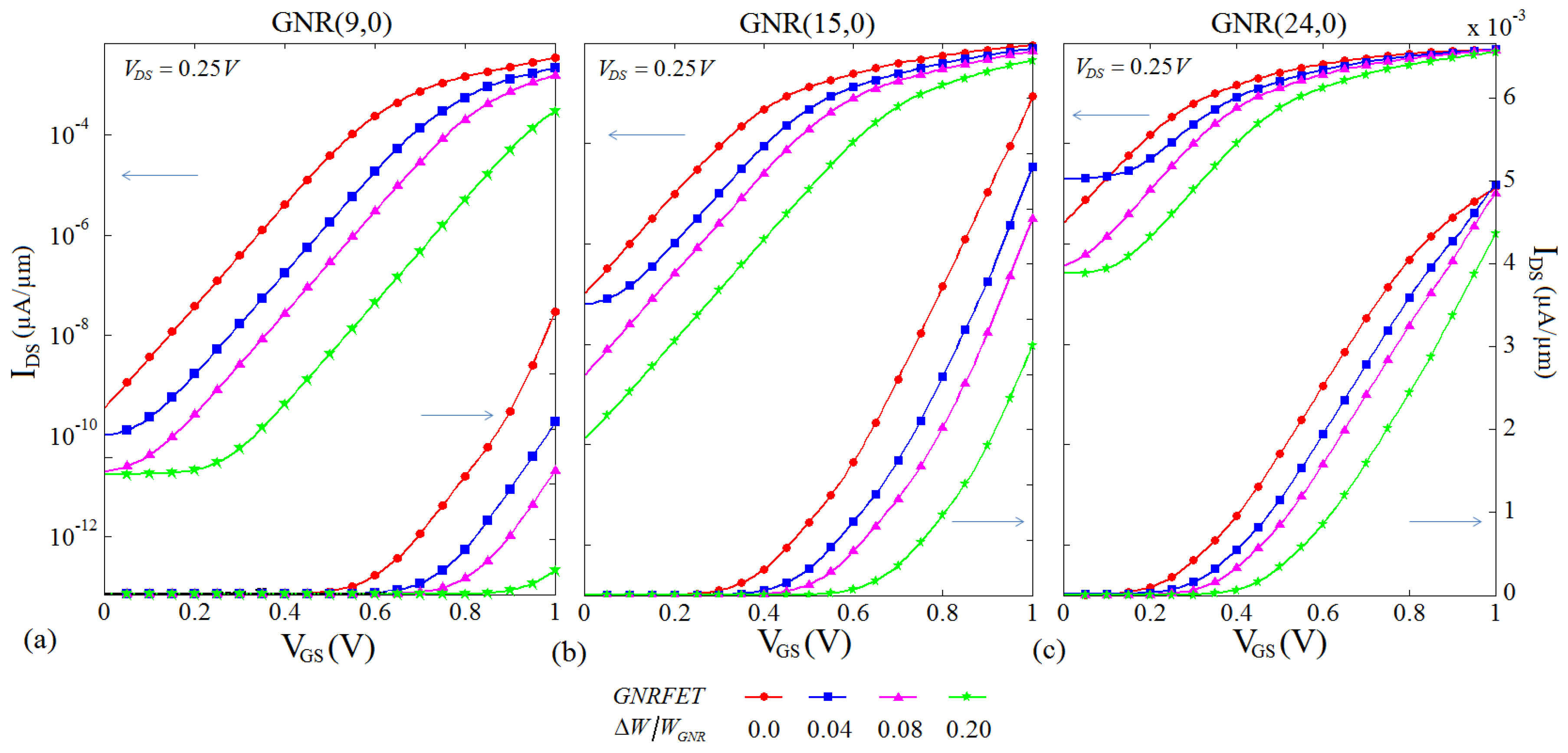
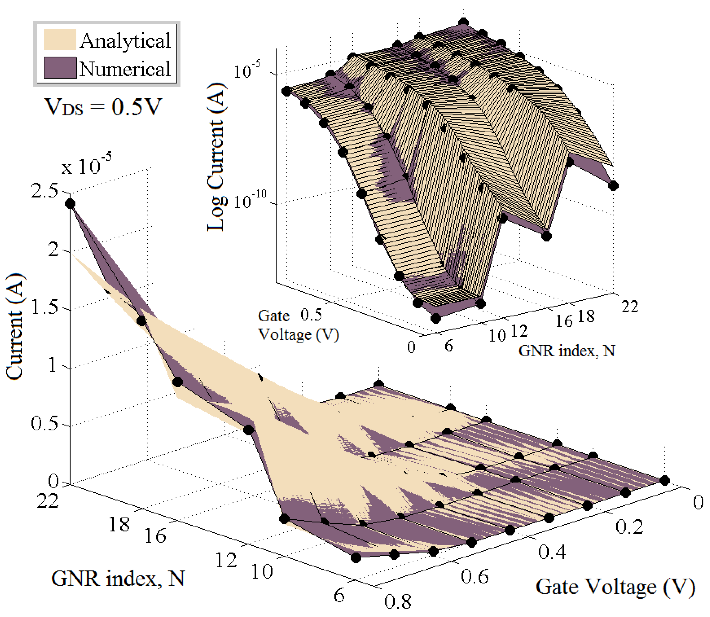
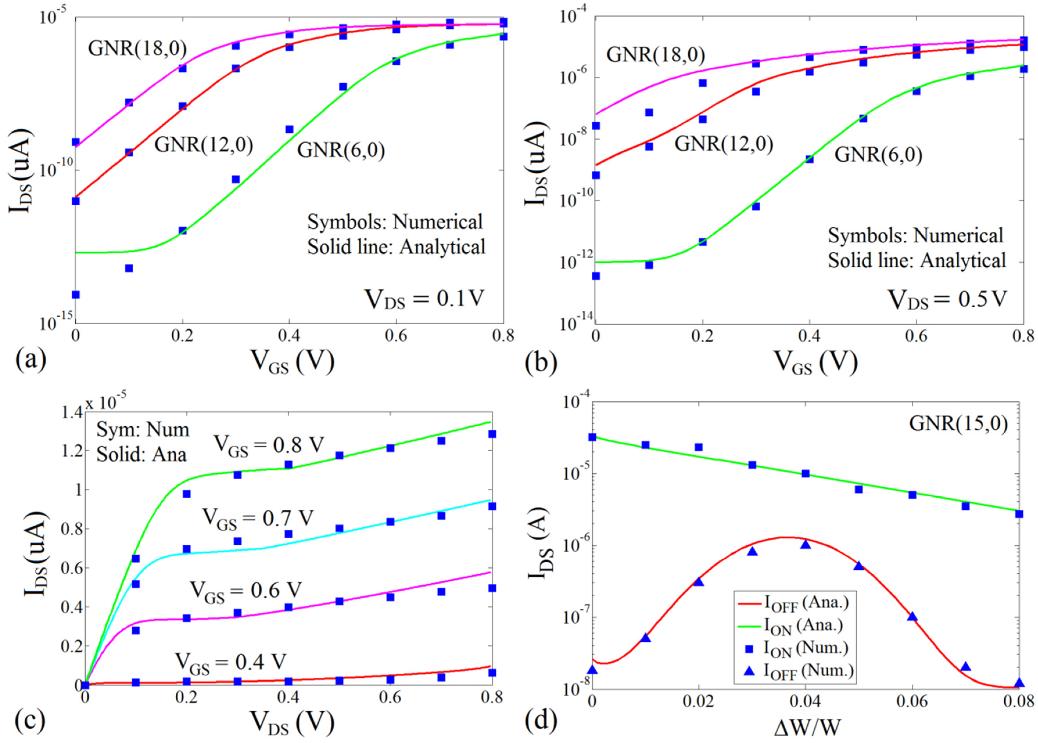
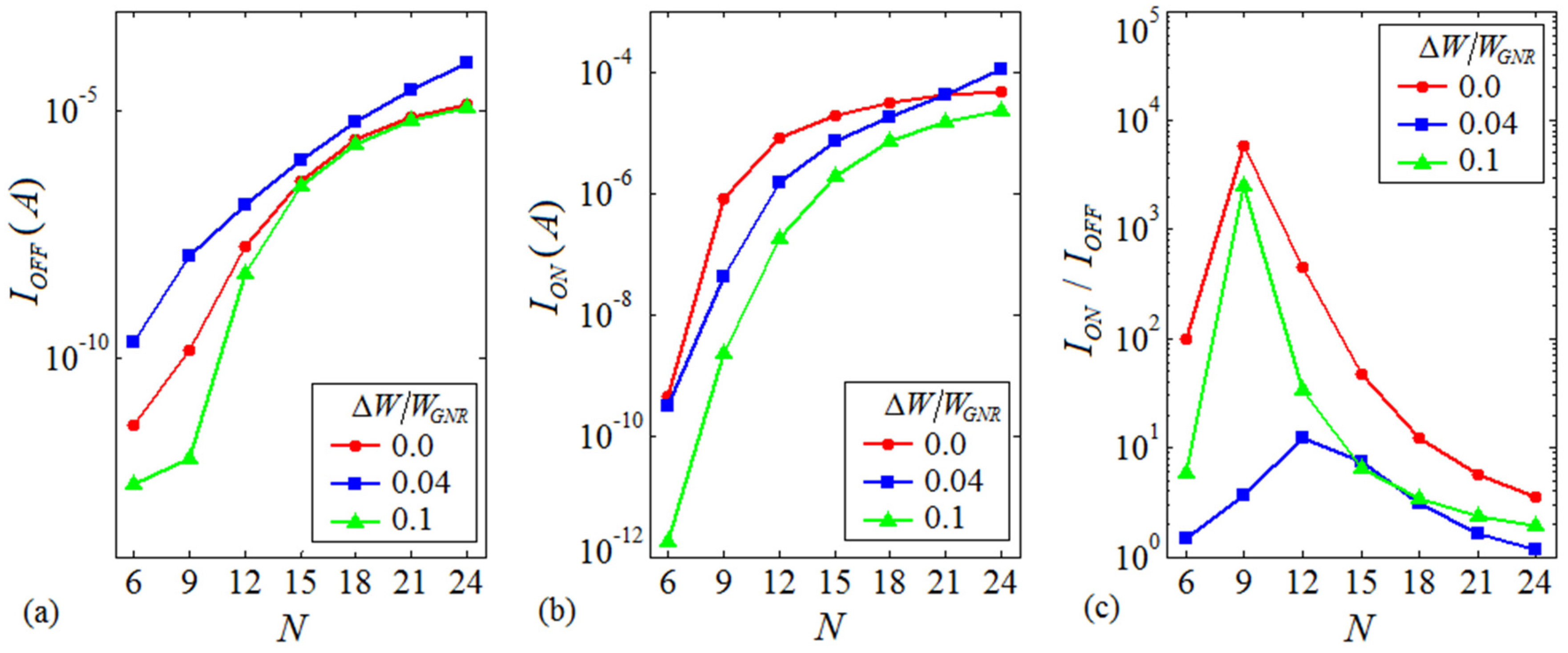
4. Model Validation
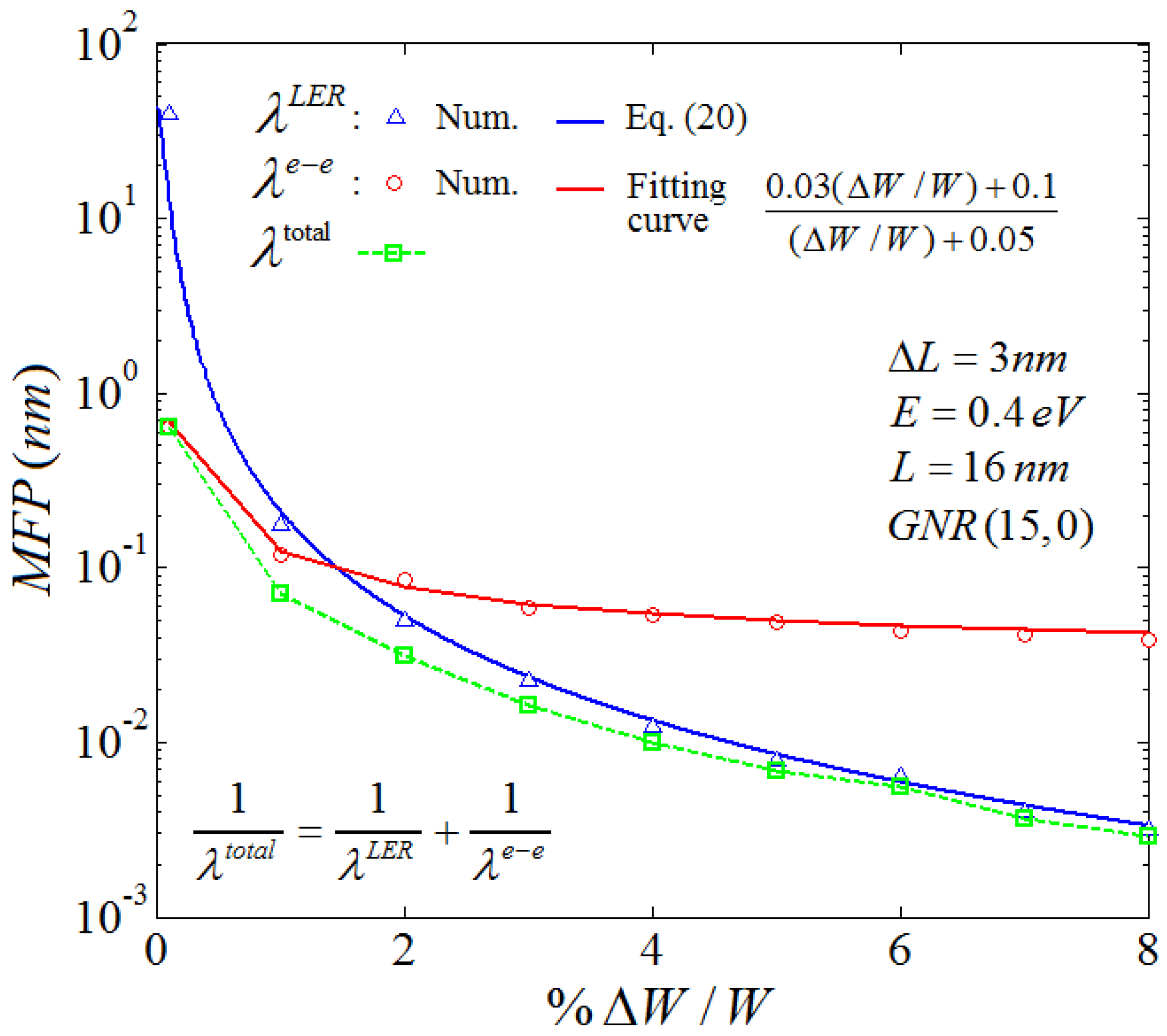
5. Validation of Single-Particle Calculations
6. Conclusions
Author Contributions
Conflicts of Interest
References
- Wilson, L. International Technology Roadmap for Semiconductors (ITRS); Semiconductor Industry Association: Washington, DC, USA, 2013. [Google Scholar]
- Novoselov, K.S.; Fal, V.; Colombo, L.; Gellert, P.; Schwab, M.; Kim, K. A roadmap for graphene. Nature 2012, 490, 192–200. [Google Scholar] [CrossRef] [PubMed]
- Obeng, Y.; De Gendt, S.; SRinivasan, P.; Misra, D.; Iwai, H.; Karim, Z.; Hess, D.; Grebel, H. Graphene and Emerging Materials for Post-CMOS Applications; Electrochemical Society: Pennington, NJ, USA, 2009. [Google Scholar]
- Novoselov, K.; Geim, A.K.; Morozov, S.; Jiang, D.; Katsnelson, M.; Grigorieva, I.; Dubonos, S.; Firsov, A. Two-dimensional gas of massless dirac fermions in graphene. Nature 2005, 438, 197–200. [Google Scholar] [CrossRef] [PubMed]
- Cooper, D.R.; D’Anjou, B.; Ghattamaneni, N.; Harack, B.; Hilke, M.; Horth, A.; Majlis, N.; Massicotte, M.; Vandsburger, L.; Whiteway, E. Experimental review of graphene. Int. Sch. Res. Not. 2012, 2012. [Google Scholar] [CrossRef]
- Schwierz, F. Graphene transistors: Status, prospects, and problems. Proc. IEEE 2013, 101, 1567–1584. [Google Scholar] [CrossRef]
- Harada, N.; Sato, S.; Yokoyama, N. Theoretical investigation of graphene nanoribbon field-effect transistors designed for digital applications. Jpn. J. Appl. Phys. 2013, 52, 094301. [Google Scholar] [CrossRef]
- Johari, Z.; Hamid, F.; Tan, M.L.P.; Ahmadi, M.T.; Harun, F.; Ismail, R. Graphene nanoribbon field effect transistor logic gates performance projection. J. Comput. Theor. Nanosci. 2013, 10, 1164–1170. [Google Scholar] [CrossRef]
- Poljak, M.; Wang, K.L.; Suligoj, T. Variability of bandgap and carrier mobility caused by edge defects in ultra-narrow graphene nanoribbons. Solid-State Electron. 2015, 108, 67–74. [Google Scholar] [CrossRef]
- Michetti, P.; Iannaccone, G. Analytical model of one-dimensional carbon-based schottky-barrier transistors. IEEE Trans. Electron Dev. 2010, 57, 1616–1625. [Google Scholar] [CrossRef]
- Choudhury, M.; Yoon, Y.; Guo, J.; Mohanram, K. Technology Exploration for Graphene Nanoribbon F s. In Proceedings of the 45th Annual Design Automation Conference, Anaheim, CA, USA, 8–13 June 2008; pp. 272–277.
- Chen, Y.-Y.; Rogachev, A.; Sangai, A.; Iannaccone, G.; Fiori, G.; Chen, D. A SPICE-Compatible Model of Graphene nano-Ribbon Field-Effect Transistors Enabling Circuit-Level Delay and Power Analysis under Process Variation. In Proceedings of the IEEE Design, Automation & Test in Europe Conference & Exhibition (DATE), Grenoble, France, 18-22 March 2013; pp. 1789–1794.
- Xu, G.; Torres Jr, C.M.; Tang, J.; Bai, J.; Song, E.B.; Huang, Y.; Duan, X.; Zhang, Y.; Wang, K.L. Edge effect on resistance scaling rules in graphene nanostructures. Nano Lett. 2011, 11, 1082–1086. [Google Scholar] [CrossRef] [PubMed]
- Yazdanpanah, A.; Pourfath, M.; Fathipour, M.; Kosina, H.; Selberherr, S. A numerical study of line-edge roughness scattering in graphene nanoribbons. IEEE Trans. Electron Dev. 2012, 59, 433–440. [Google Scholar] [CrossRef]
- Yoon, Y.; Fiori, G.; Hong, S.; Iannaccone, G.; Guo, J. Performance comparison of graphene nanoribbon fets with schottky contacts and doped reservoirs. IEEE Trans. Electron Dev. 2008, 55, 2314–2323. [Google Scholar] [CrossRef]
- Kang, J.; Sarkar, D.; Khatami, Y.; Banerjee, K. Proposal for all-graphene monolithic logic circuits. Appl. Phys. Lett. 2013, 103, 083113. [Google Scholar] [CrossRef]
- Owlia, H.; Keshavarzi, P. Investigation of the novel attributes of a double-gate graphene nanoribbon fet with aln high-κ dielectrics. Superlattices Microstruct. 2014, 75, 613–620. [Google Scholar] [CrossRef]
- Oh, J.G.; Hong, S.K.; Kim, C.-K.; Bong, J.H.; Shin, J.; Choi, S.-Y.; Cho, B.J. High performance graphene field effect transistors on an aluminum nitride substrate with high surface phonon energy. Appl. Phys. Lett. 2014, 104, 193112. [Google Scholar]
- Konar, A.; Fang, T.; Jena, D. Effect of high-k dielectrics on charge transport in graphene. 2009; arXiv:0902.0819. [Google Scholar]
- Banadaki, Y.; Srivastava, A. Scaling effects on static metrics and switching attributes of graphene nanoribbon fet for emerging technology. IEEE Trans. Emerg. Top. Comput. 2015, 4, 458–469. [Google Scholar] [CrossRef]
- Grassi, R.; Poli, S.; Gnani, E.; Gnudi, A.; Reggiani, S.; Baccarani, G. Tight-binding and effective mass modeling of armchair graphene nanoribbon fets. Solid-State Electron. 2009, 53, 462–467. [Google Scholar] [CrossRef]
- Banadaki, Y.M.; Srivastava, A. Investigation of the width-dependent static characteristics of graphene nanoribbon field effect transistors using non-parabolic quantum-based model. Solid-State Electron. 2015, 111, 80–90. [Google Scholar] [CrossRef]
- Kliros, G.S. Scaling Effects on the Gate Capacitance of Graphene Nanoribbon Transistors. In Proceedings of the IEEE International Semiconductor Conference (CAS), Sinaia, Romania, 15–17 October 2012; pp. 83–86.
- Deng, J.; Wong, H.P. A compact spice model for carbon-nanotube field-effect transistors including nonidealities and its application-part i: Model of the intrinsic channel region. IEEE Trans. Electron Dev. 2007, 54, 3186–3194. [Google Scholar] [CrossRef]
- Gholipour, M.; Chen, Y.-Y.; Sangai, A.; Chen, D. Highly Accurate SPICE-Compatible Modeling for Single-and Double-Gate Gnrfets with Studies on Technology Scaling. In Proceedings of the Conference on Design, Automation & Test in Europe, Dresden, Germany, 24–28 March 2014; p. 120.
- Capacitor Calculator. Available online: http://www.Technick.Net/public/code/cp_dpage.Php?Aiocp_dp=util_ pcb_imp_microstrip_embed (accessed on 7 January 2015).
- Garg, R.; Bahl, I.; Bozzi, M. Microstrip Lines and Slotlines; Artech house: Norwood, MA, USA, 2013. [Google Scholar]
- Wang, J.; Lundstrom, M. Does Source-to-Drain Tunneling Limit the Ultimate Scaling of Mosfets? In Proceedings of the IEEE International Electron Devices Meeting (IEDM'02), San Francisco, CA, USA, 8–11 December 2002; pp. 707–710.
- Datta, S. Quantum Transport: Atom to Transistor; Cambridge University Press: Cambridge, UK, 2005. [Google Scholar]
- Kane, E.O. Theory of tunneling. J. Appl. Phys. 1961, 32, 83–91. [Google Scholar] [CrossRef]
- Geist, J.; Lowney, J. Effect of band-gap narrowing on the built-in electric field in n-type silicon. J. Appl. Phys. 1981, 52, 1121–1123. [Google Scholar] [CrossRef]
- Geim, A.K.; Novoselov, K.S. The rise of graphene. Nat. Mater. 2007, 6, 183–191. [Google Scholar] [CrossRef] [PubMed]
- Akturk, A.; Goldsman, N. Electron transport and full-band electron-phonon interactions in graphene. J. Appl. Phys. 2008, 103, 053702. [Google Scholar] [CrossRef]
- Chen, J.-H.; Jang, C.; Xiao, S.; Ishigami, M.; Fuhrer, M.S. Intrinsic and extrinsic performance limits of graphene devices on sio2. Nat. Nanotechnol. 2008, 3, 206–209. [Google Scholar] [CrossRef] [PubMed]
- Yang, Y.; Murali, R. Impact of size effect on graphene nanoribbon transport. IEEE Electron Dev. Lett. 2010, 31, 237–239. [Google Scholar] [CrossRef]
- Zhao, P.; Choudhury, M.; Mohanram, K.; Guo, J. Computational model of edge effects in graphene nanoribbon transistors. Nano Res. 2008, 1, 395–402. [Google Scholar] [CrossRef]
- Lundstrom, M.; Guo, J. Nanoscale Transistors: Device Physics, Modeling and Simulation; Springer Science & Business Media: New York, NY, USA, 2006. [Google Scholar]
- Perebeinos, V.; Tersoff, J.; Avouris, P. Electron-phonon interaction and transport in semiconducting carbon nanotubes. Phys. Rev. Lett. 2005, 94, 086802. [Google Scholar] [CrossRef] [PubMed]
- Rakheja, S.; Kumar, V.; Naeemi, A. Evaluation of the potential performance of graphene nanoribbons as on-chip interconnects. Proc. IEEE 2013, 101, 1740–1765. [Google Scholar] [CrossRef]
- Wang, X.; Ouyang, Y.; Li, X.; Wang, H.; Guo, J.; Dai, H. Room-temperature all-semiconducting sub-10-nm graphene nanoribbon field-effect transistors. Phys. Rev. Lett. 2008, 100, 206803. [Google Scholar] [CrossRef] [PubMed]
- Areshkin, D.A.; Gunlycke, D.; White, C.T. Ballistic transport in graphene nanostrips in the presence of disorder: Importance of edge effects. Nano Lett. 2007, 7, 204–210. [Google Scholar] [CrossRef] [PubMed]
- Gunlycke, D.; Areshkin, D.; White, C. Semiconducting graphene nanostrips with edge disorder. Appl. Phys. Lett. 2007, 90, 142104. [Google Scholar] [CrossRef]
- Gunlycke, D.; White, C. Scaling of the localization length in armchair-edge graphene nanoribbons. Phys. Rev. B 2010, 81, 075434. [Google Scholar] [CrossRef]
- Goodnick, S.; Ferry, D.; Wilmsen, C.; Liliental, Z.; Fathy, D.; Krivanek, O. Surface roughness at the Si(100)-Sio2 interface. Phys. Rev. B 1985, 32, 8171. [Google Scholar] [CrossRef]
- Fang, T.; Konar, A.; Xing, H.; Jena, D. Mobility in semiconducting graphene nanoribbons: Phonon, impurity, and edge roughness scattering. Phys. Rev. B 2008, 78, 205403. [Google Scholar] [CrossRef]
- Goharrizi, A.Y.; Pourfath, M.; Fathipour, M.; Kosina, H.; Selberherr, S. An analytical model for line-edge roughness limited mobility of graphene nanoribbons. IEEE Trans. Electron Dev. 2011, 58, 3725–3735. [Google Scholar] [CrossRef]
- Luisier, M.; Klimeck, G. Performance analysis of statistical samples of graphene nanoribbon tunneling transistors with line edge roughness. Appl. Phys. Lett. 2009, 94, 223505. [Google Scholar] [CrossRef]
- Bai, J.; Duan, X.; Huang, Y. Rational fabrication of graphene nanoribbons using a nanowire etch mask. Nano Lett. 2009, 9, 2083–2087. [Google Scholar] [CrossRef] [PubMed]
- Lin, M.-W.; Ling, C.; Zhang, Y.; Yoon, H.J.; Cheng, M.M.-C.; Agapito, L.A.; Kioussis, N.; Widjaja, N.; Zhou, Z. Room-temperature high on/off ratio in suspended graphene nanoribbon field-effect transistors. Nanotechnology 2011, 22, 265201. [Google Scholar] [CrossRef] [PubMed]
- Huang, C.-H.; Su, C.-Y.; Okada, T.; Li, L.-J.; Ho, K.-I.; Li, P.-W.; Chen, I.-H.; Chou, C.; Lai, C.-S.; Samukawa, S. Ultra-low-edge-defect graphene nanoribbons patterned by neutral beam. Carbon 2013, 61, 229–235. [Google Scholar] [CrossRef]
- Yoon, Y.; Guo, J. Effect of edge roughness in graphene nanoribbon transistors. Appl. Phys. Lett. 2007, 91, 073103. [Google Scholar] [CrossRef]
- Fiori, G.; Iannaccone, G. Simulation of graphene nanoribbon field-effect transistors. Electron Dev. Lett. IEEE 2007, 28, 760–762. [Google Scholar] [CrossRef]
- Sprinkle, M.; Ruan, M.; Hu, Y.; Hankinson, J.; Rubio-Roy, M.; Zhang, B.; Wu, X.; Berger, C.; De Heer, W.A. Scalable templated growth of graphene nanoribbons on SiC. Nat. Nanotechnol. 2010, 5, 727–731. [Google Scholar] [CrossRef] [PubMed]
- Evaldsson, M.; Zozoulenko, I.V.; Xu, H.; Heinzel, T. Edge-disorder-induced anderson localization and conduction gap in graphene nanoribbons. Phys. Rev. B 2008, 78, 161407. [Google Scholar] [CrossRef]
- Kahnoj, S.S.; Touski, S.B.; Pourfath, M. The effect of electron-electron interaction induced dephasing on electronic transport in graphene nanoribbons. Appl. Phys. Lett. 2014, 105, 103502. [Google Scholar] [CrossRef]
- Li, X.; Barry, E.; Zavada, J.; Nardelli, M.B.; Kim, K. Influence of electron-electron scattering on transport characteristics in monolayer graphene. Appl. Phys. Lett. 2010, 97, 082101. [Google Scholar] [CrossRef]
- Lherbier, A.; Biel, B.; Niquet, Y.-M.; Roche, S. Transport length scales in disordered graphene-based materials: Strong localization regimes and dimensionality effects. Phys. Rev. Lett. 2008, 100, 036803. [Google Scholar] [CrossRef] [PubMed]
- Datta, S. Electronic Transport in Mesoscopic Systems; Cambridge University Press: Cambridge, UK, 1997. [Google Scholar]
- Bischoff, D.; Varlet, A.; Simonet, P.; Eich, M.; Overweg, H.; Ihn, T.; Ensslin, K. Localized charge carriers in graphene nanodevices. Appl. Phys. Rev. 2015, 2, 031301. [Google Scholar] [CrossRef]
- Sols, F.; Guinea, F.; Neto, A.C. Coulomb blockade in graphene nanoribbons. Phys. Rev. Lett. 2007, 99, 166803. [Google Scholar] [CrossRef] [PubMed]


| Fitting Parameter | Obtained Value | Searching Range | Searching Step | % RMSE |
|---|---|---|---|---|
| lrelax | 40 nm | 10 nm–100 nm | 5 nm | <10% |
| δ | 0.05 | 0.01–0.1 | 0.025 | |
| γ | 2.9 | 0–3 | 0.5, then 0.1 | <20% |
| 6 × 10⁻⁶ | From 0 | Different (Nonlinear) | ||
| 0.0145 | From 0 | 0.01, 0.001 and 0.0001 |
| Device Dimension | GNR Channel Length () | |
| GNR Channel Width (WGNR, GNR(N,0)) | ||
| Oxide Thickness () | ||
| Line-edge Roughness | Roughness Amplitude () | |
| Roughness Correlation () |
© 2016 by the authors; licensee MDPI, Basel, Switzerland. This article is an open access article distributed under the terms and conditions of the Creative Commons by Attribution (CC-BY) license (http://creativecommons.org/licenses/by/4.0/).
Share and Cite
Banadaki, Y.M.; Srivastava, A. Effect of Edge Roughness on Static Characteristics of Graphene Nanoribbon Field Effect Transistor. Electronics 2016, 5, 11. https://doi.org/10.3390/electronics5010011
Banadaki YM, Srivastava A. Effect of Edge Roughness on Static Characteristics of Graphene Nanoribbon Field Effect Transistor. Electronics. 2016; 5(1):11. https://doi.org/10.3390/electronics5010011
Chicago/Turabian StyleBanadaki, Yaser M., and Ashok Srivastava. 2016. "Effect of Edge Roughness on Static Characteristics of Graphene Nanoribbon Field Effect Transistor" Electronics 5, no. 1: 11. https://doi.org/10.3390/electronics5010011
APA StyleBanadaki, Y. M., & Srivastava, A. (2016). Effect of Edge Roughness on Static Characteristics of Graphene Nanoribbon Field Effect Transistor. Electronics, 5(1), 11. https://doi.org/10.3390/electronics5010011