
Scalable Fabrication of 2D Semiconducting Crystals for Future Electronics

Abstract
:1. Introduction
2. Scalable Synthesis Techniques for TMDCs
2.1. Vapor Phase Deposition
2.1.1. Solid-Precursor VPD


2.1.2. Gas-Precursor VPD


2.2. Thermal Decomposition

2.3. Magnetron Sputtering
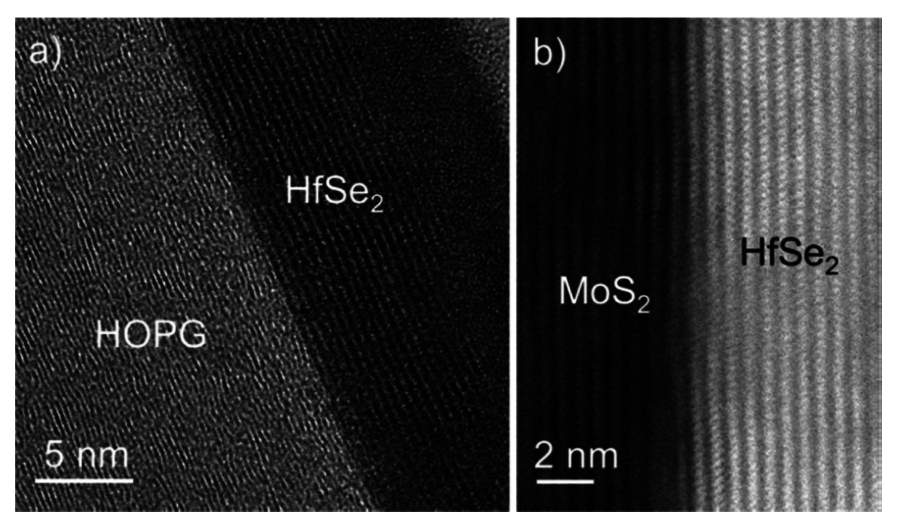
2.4. Molecular Beam Epitaxy


3. Advanced Engineering for Materials, Heterostructures and Devices
3.1. TMDC Alloys
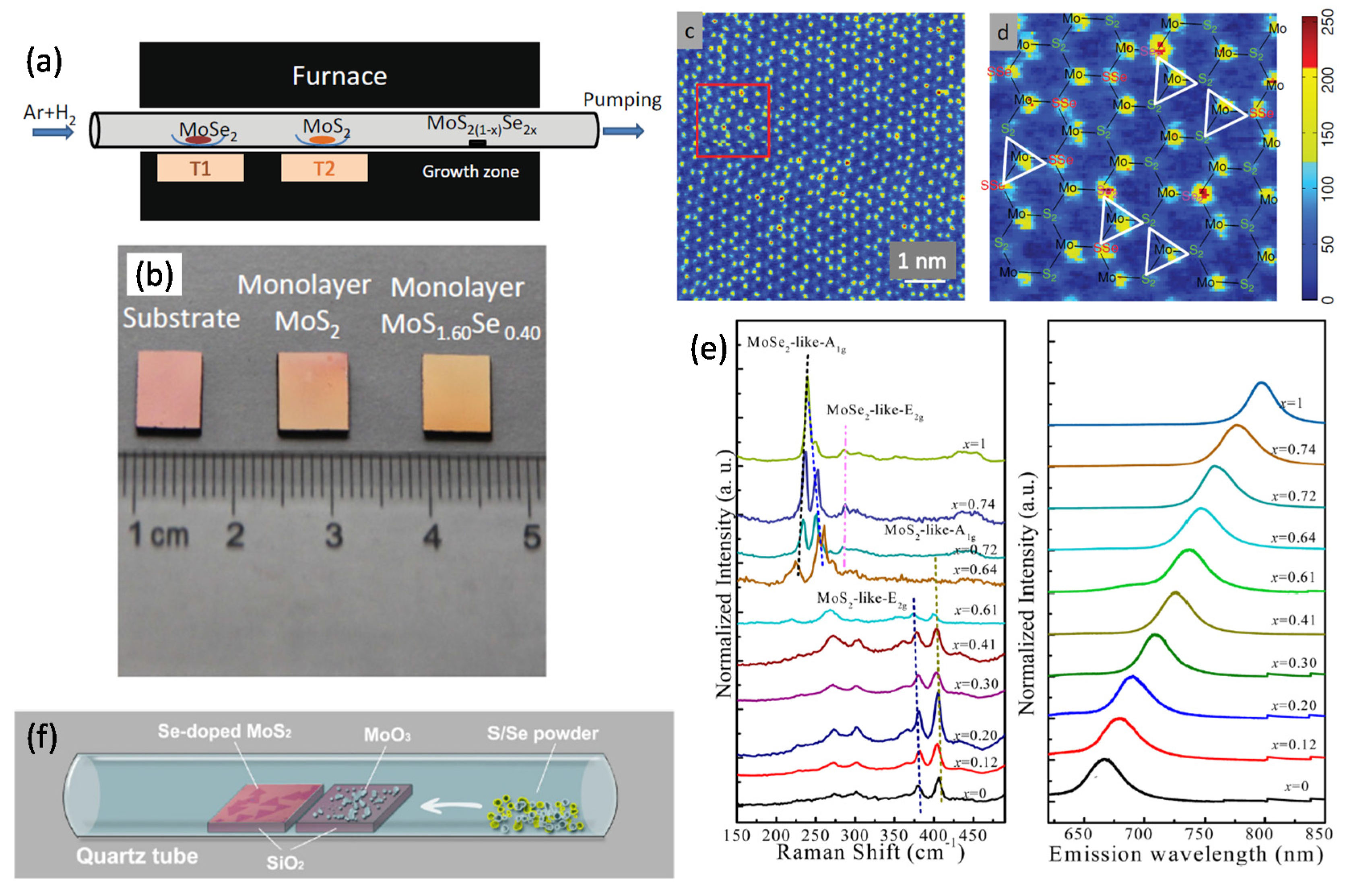
3.1.1. MoS2(1−x)Se2x Alloys

3.1.2. Mo1−xWxS2 Alloys

3.2. 2D Heterostructures
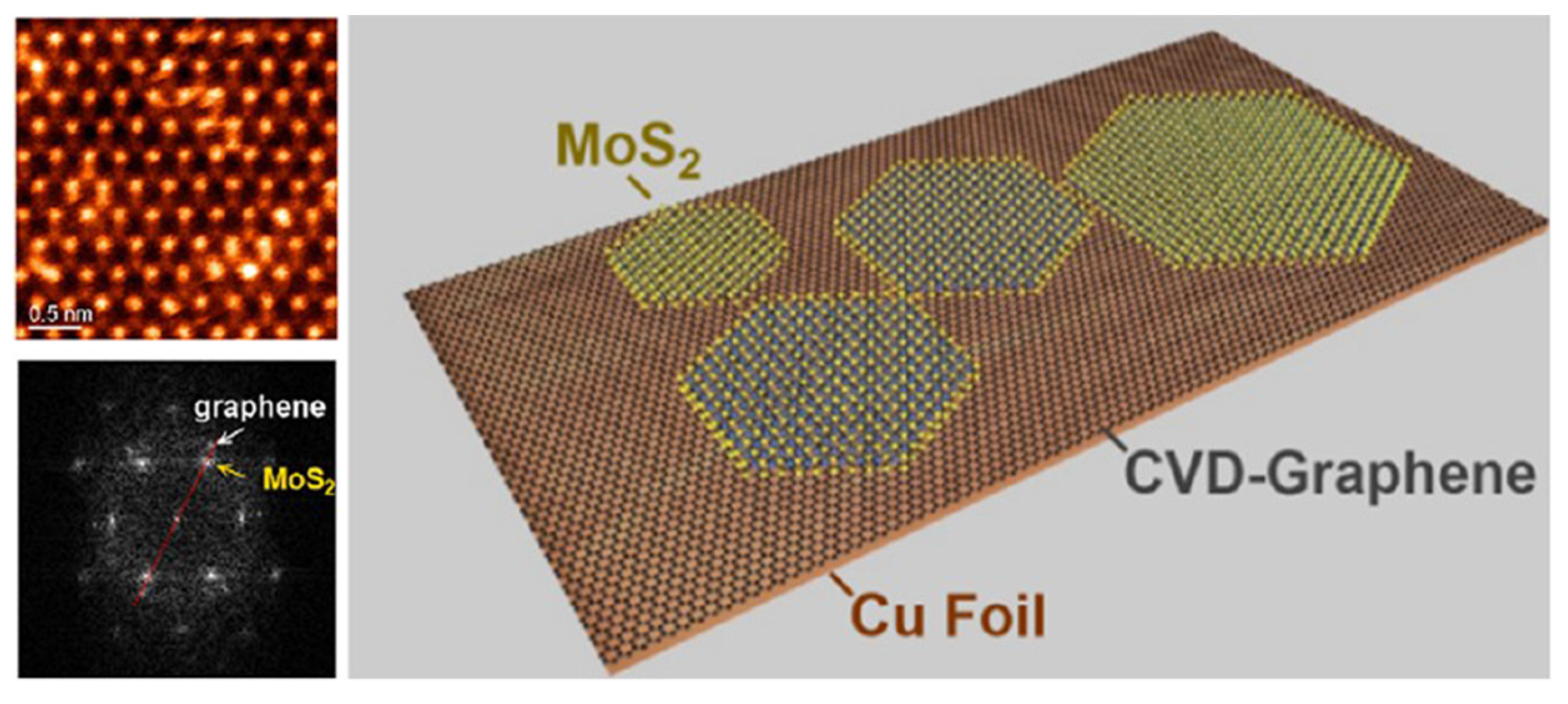
3.2.1. TMDC/Graphene Heterostructures

3.2.2. TMDC/BN Heterostructures

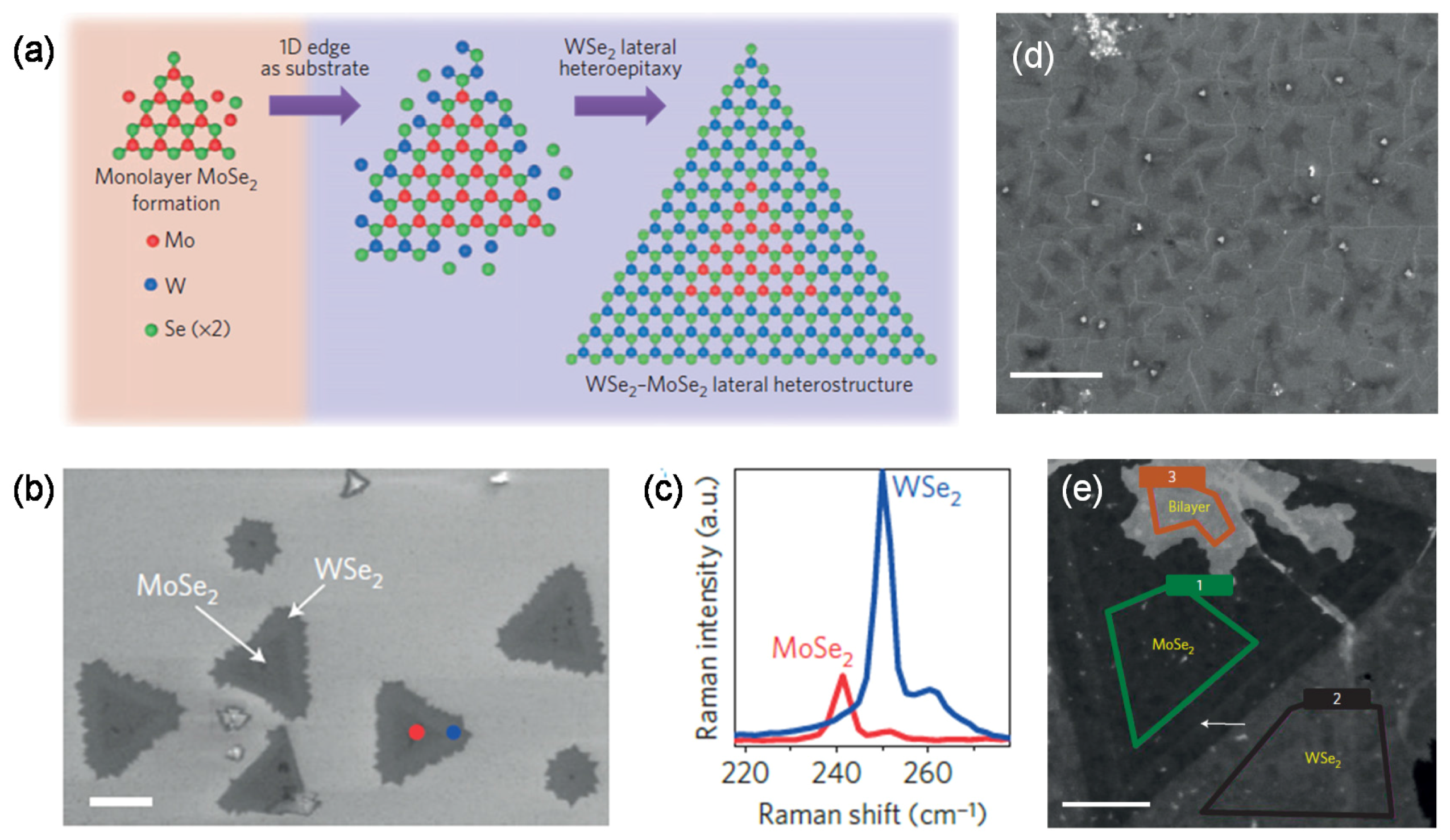
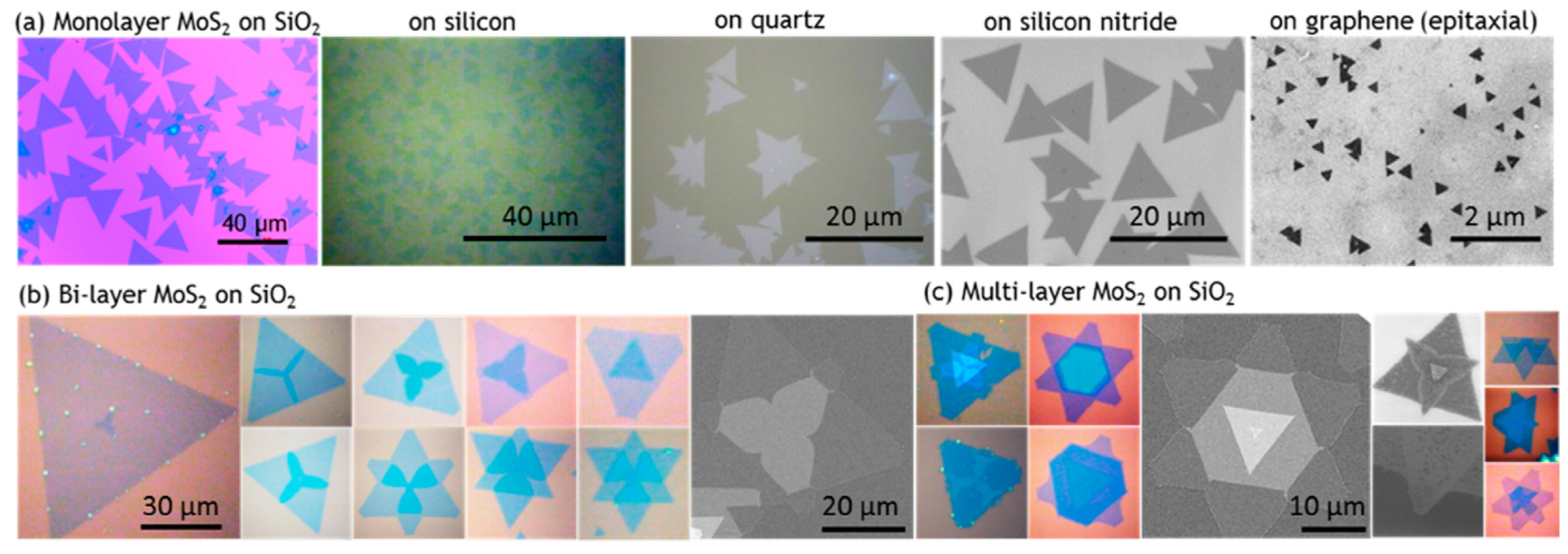
3.2.3. TMDC/TMDC Heterostructures


3.3. Wafer-Scale Device Engineering
3.3.1. Direct Growth of TMDC at Controlled Locations

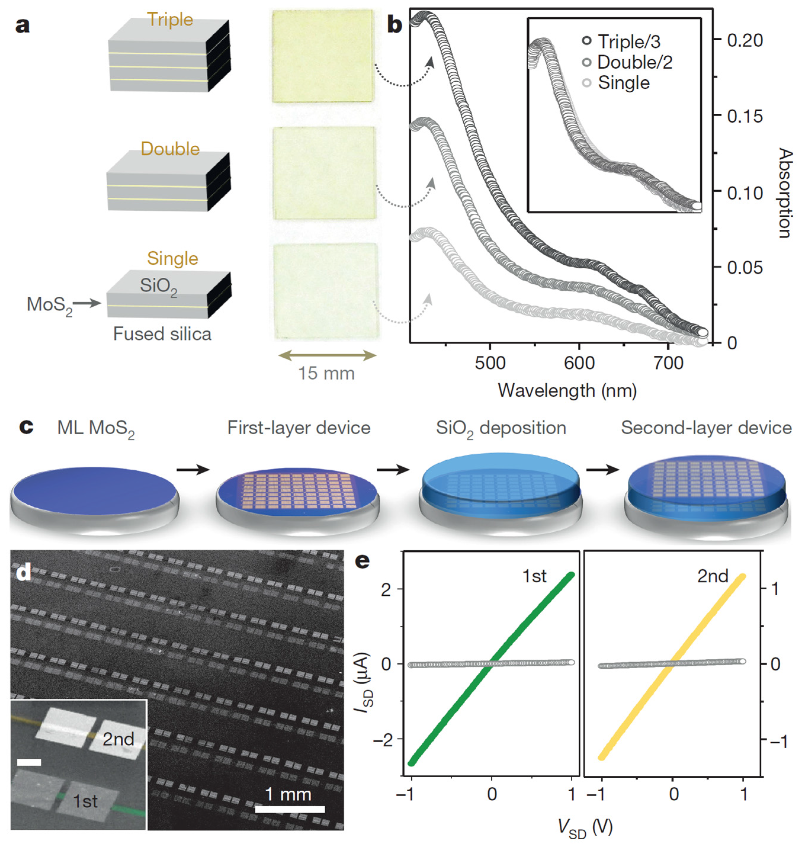
3.3.2. Multi-Level Stacking of TMDC Devices

4. Discussions and Outlook


Acknowledgments
Author Contributions
Conflicts of Interest
References
- Novoselov, K.S.; Fal’ko, V.I.; Colombo, L.; Gellert, P.R.; Schwab, M.G.; Kim, K. A roadmap for graphene. Nature 2012, 490, 192–200. [Google Scholar] [CrossRef] [PubMed]
- Wang, Q.H.; Kalantar-Zadeh, K.; Kis, A.; Coleman, J.N.; Strano, M.S. Electronics and optoelectronics of two-dimensional transition metal dichalcogenides. Nat. Nanotechnol. 2012, 7, 699–712. [Google Scholar] [CrossRef] [PubMed]
- Kim, S.J.; Choi, K.; Lee, B.; Kim, Y.; Hong, B.H. Materials for Flexible, Stretchable Electronics: Graphene and 2D Materials. Annu. Rev. Mater. Res. 2015, 45, 63–84. [Google Scholar] [CrossRef]
- Vaziri, S.; Lupina, G.; Henkel, C.; Smith, A.D.; Östling, M.; Dabrowski, J.; Lippert, G.; Mehr, W.; Lemme, M.C. A Graphene-Based Hot Electron Transistor. Nano Lett. 2013, 13, 1435–1439. [Google Scholar] [CrossRef] [PubMed]
- Lemme, M.C.; Li, L.-J.; Palacios, T.; Schwierz, F. Two-dimensional materials for electronic applications. MRS Bull. 2014, 39, 711–718. [Google Scholar] [CrossRef]
- Lemme, M.C.; Echtermeyer, T.J.; Baus, M.; Kurz, H. A Graphene Field-Effect Device. IEEE Electron Device Lett. 2007, 28, 282–284. [Google Scholar] [CrossRef]
- Lopez-Sanchez, O.; Lembke, D.; Kayci, M.; Radenovic, A.; Kis, A. Ultrasensitive photodetectors based on monolayer MoS2. Nat. Nanotechnol. 2013, 8, 497–501. [Google Scholar] [CrossRef] [PubMed]
- Yim, C.; O’Brien, M.; McEvoy, N.; Riazimehr, S.; Schäfer-Eberwein, H.; Bablich, A.; Pawar, R.; Iannaccone, G.; Downing, C.; Fiori, G.; et al. Heterojunction Hybrid Devices from Vapor Phase Grown MoS2. Sci. Rep. 2014, 4, 5458. [Google Scholar] [CrossRef] [PubMed]
- Li, J.; Lemme, M.C.; Östling, M. Inkjet Printing of 2D Layered Materials. Chemphyschem 2014, 15, 3427–3434. [Google Scholar] [CrossRef] [PubMed]
- Li, J.; Östling, M. Prevention of Graphene Restacking for Performance Boost of Supercapacitors—A Review. Crystals 2013, 3, 163–190. [Google Scholar] [CrossRef]
- Smith, A.D.; Niklaus, F.; Paussa, A.; Vaziri, S.; Fischer, A.C.; Sterner, M.; Forsberg, F.; Delin, A.; Esseni, D.; Palestri, P.; et al. Electromechanical Piezoresistive Sensing in Suspended Graphene Membranes. Nano Lett. 2013, 13, 3237–3242. [Google Scholar] [CrossRef] [PubMed]
- Shen, H.; Zhang, L.; Liu, M.; Zhang, Z. Biomedical applications of graphene. Theranostics 2012, 2, 283–294. [Google Scholar] [CrossRef] [PubMed]
- Geim, A.K.; Grigorieva, I.V. Van der Waals heterostructures. Nature 2013, 499, 419–425. [Google Scholar] [CrossRef] [PubMed]
- Radisavljevic, B.; Radenovic, A.; Brivio, J.; Giacometti, V.; Kis, A. Single-layer MoS2 transistors. Nat. Nanotechnol. 2011, 6, 147–150. [Google Scholar] [CrossRef] [PubMed]
- Liu, H.; Du, Y.; Deng, Y.; Ye, P.D. Semiconducting black phosphorus: Synthesis, transport properties and electronic applications. Chem. Soc. Rev. 2015, 44, 2732–2743. [Google Scholar] [CrossRef] [PubMed]
- Nicolosi, V.; Chhowalla, M.; Kanatzidis, M.G.; Strano, M.S.; Coleman, J.N. Liquid Exfoliation of Layered Materials. Science 2013, 340. [Google Scholar] [CrossRef]
- Li, J.; Ye, F.; Vaziri, S.; Muhammed, M.; Lemme, M.C.; Östling, M. Efficient Inkjet Printing of Graphene. Adv. Mater. 2013, 25, 3985–3992. [Google Scholar] [CrossRef] [PubMed]
- Li, J.; Naiini, M.M.; Vaziri, S.; Lemme, M.C.; Östling, M. Inkjet Printing of MoS2. Adv. Funct. Mater. 2014, 24, 6524–6531. [Google Scholar] [CrossRef]
- Kong, D.; Wang, H.; Cha, J.J.; Pasta, M.; Koski, K.J.; Yao, J.; Cui, Y. Synthesis of MoS2 and MoSe2 Films with Vertically Aligned Layers. Nano Lett. 2013, 13, 1341–1347. [Google Scholar] [CrossRef] [PubMed]
- Shi, Y.; Li, H.; Li, L.J. Recent advances in controlled synthesis of two-dimensional transition metal dichalcogenides via vapor deposition techniques. Chem. Soc. Rev. 2015, 44, 2744–2756. [Google Scholar] [CrossRef] [PubMed]
- Najmaei, S.; Liu, Z.; Zhou, W.; Zou, X.; Shi, G.; Lei, S.; Yakobson, B.I.; Idrobo, J.-C.; Ajayan, P.M.; Lou, J. Vapour phase growth and grain boundary structure of molybdenum disulphide atomic layers. Nat. Mater. 2013, 12, 754–759. [Google Scholar] [CrossRef] [PubMed]
- Ling, X.; Lee, Y.-H.; Lin, Y.; Fang, W.; Yu, L.; Dresselhaus, M.S.; Kong, J. Role of the Seeding Promoter in MoS2 Growth by Chemical Vapor Deposition. Nano Lett. 2014, 14, 464–472. [Google Scholar] [CrossRef] [PubMed]
- Kang, K.; Xie, S.; Huang, L.; Han, Y.; Huang, P.Y.; Mak, K.F.; Kim, C.-J.; Muller, D.; Park, J. High-mobility three-atom-thick semiconducting films with wafer-scale homogeneity. Nature 2015, 520, 656–660. [Google Scholar] [CrossRef] [PubMed]
- Dumcenco, D.; Ovchinnikov, D.; Marinov, K.; Lazić, P.; Gibertini, M.; Marzari, N.; Sanchez, O.L.; Kung, Y.; Krasnozhon, D.; Chen, M.; et al. Large-Area Epitaxial Monolayer MoS2. ACS Nano 2015, 9, 4611–4620. [Google Scholar] [CrossRef] [PubMed]
- Zhang, Y.; Zhang, Y.; Ji, Q.; Ju, J.; Yuan, H.; Shi, J.; Gao, T.; Ma, D.; Liu, M.; Chen, Y.; et al. Controlled Growth of High-Quality Monolayer WS2 Layers on Sapphire and Imaging Its Grain Boundary. ACS Nano 2013, 7, 8963–8971. [Google Scholar] [CrossRef] [PubMed]
- Lee, Y.H.; Zhang, X.Q.; Zhang, W.; Chang, M.T.; Lin, C.T.; Chang, K.D.; Yu, Y.C.; Wang, J.T.W.; Chang, C.S.; Li, L.J.; et al. Synthesis of large-area MoS2 atomic layers with chemical vapor deposition. Adv. Mater. 2012, 24, 2320–2325. [Google Scholar] [CrossRef] [PubMed]
- Lee, Y.; Yu, L.; Wang, H.; Fang, W.; Ling, X.; Shi, Y.; Lin, C.-T.; Huang, J.-K.; Chang, M.-T.; Chang, C.-S.; et al. Synthesis and Transfer of Single Layer Transition Metal Disulfides on Diverse Surfaces. Nano Lett. 2013, 13, 1852–1857. [Google Scholar] [CrossRef] [PubMed]
- Song, J.; Park, J.; Lee, W.; Choi, T.; Jung, H.; Lee, C.W.; Hwang, S.-H.; Myoung, J.M.; Jung, J.-H.; Kim, S.; et al. Layer-Controlled, Wafer-Scale, and Conformal Synthesis of Tungsten Disulfide Nanosheets Using Atomic Layer Deposition. ACS Nano 2013, 7, 11333–11340. [Google Scholar] [CrossRef] [PubMed]
- Jeon, J.; Jang, S.K.; Jeon, S.M.; Yoo, G.; Jang, Y.H.; Park, J.-H.; Lee, S. Layer-controlled CVD growth of large-area two-dimensional MoS2 films. Nanoscale 2015, 7, 1688–1695. [Google Scholar] [CrossRef] [PubMed]
- Bilgin, I.; Liu, F.; Vargas, A.; Winchester, A.; Man, M.K.L.; Upmanyu, M.; Dani, K.M.; Gupta, G.; Talapatra, S.; Mohite, A.D.; et al. Chemical Vapor Deposition Synthesized Atomically Thin Molybdenum Disulfide with Optoelectronic-Grade Crystalline Quality. ACS Nano 2015, 9, 8822–8832. [Google Scholar] [CrossRef] [PubMed]
- Yu, Y.; Li, C.; Liu, Y.; Su, L.; Zhang, Y.; Cao, L. Controlled scalable synthesis of uniform, high-quality monolayer and few-layer MoS2 films. Sci. Rep. 2013, 3, 1866. [Google Scholar] [CrossRef] [PubMed]
- Grønborg, S.S.; Ulstrup, S.; Bianchi, M.; Dendzik, M.; Sanders, C.E.; Lauritsen, J.V.; Hofmann, P.; Miwa, J.A. Synthesis of Epitaxial Single-Layer MoS2 on Au(111). Langmuir 2015, 31, 9700–9706. [Google Scholar] [CrossRef] [PubMed]
- Liu, K.-K.; Zhang, W.; Lee, Y.-H.; Lin, Y.-C.; Chang, M.-T.; Su, C.-Y.; Chang, C.-S.; Li, H.; Shi, Y.; Zhang, H.; et al. Growth of large-area and highly crystalline MoS2 thin layers on insulating substrates. Nano Lett. 2012, 12, 1538–1544. [Google Scholar] [CrossRef] [PubMed]
- Tao, J.; Chai, J.; Lu, X.; Wong, L.M.; Wong, T.I.; Pan, J.; Xiong, Q.; Chi, D.; Wang, S. Growth of wafer-scale MoS2 monolayer by magnetron sputtering. Nanoscale 2015, 7, 2497–2503. [Google Scholar] [CrossRef] [PubMed]
- Yue, R.; Barton, A.T.; Zhu, H.; Azcatl, A.; Pena, L.F.; Wang, J.; Peng, X.; Lu, N.; Cheng, L.; Addou, R.; et al. HfSe2 Thin Films: 2D Transition Metal Dichalcogenides Grown by Molecular Beam Epitaxy. ACS Nano 2015, 9, 474–480. [Google Scholar] [CrossRef] [PubMed]
- Zhang, W.; Li, X.; Jiang, T.; Song, J.; Lin, Y.; Zhu, L.; Xu, X. CVD synthesis of Mo(1−x)WxS2 and MoS2(1−x)Se2x alloy monolayers aimed at tuning the bandgap of molybdenum disulfide. Nanoscale 2015, 7, 13554–13560. [Google Scholar] [CrossRef] [PubMed]
- Feng, Q.; Zhu, Y.; Hong, J.; Zhang, M.; Duan, W.; Mao, N.; Wu, J.; Xu, H.; Dong, F.; Lin, F.; et al. Growth of large-area 2D MoS2(1−x)Se2x semiconductor alloys. Adv. Mater. 2014, 26, 2648–2653. [Google Scholar] [CrossRef] [PubMed]
- Feng, Q.; Mao, N.; Wu, J.; Xu, H.; Wang, C.; Zhang, J.; Xie, L. Growth of MoS2(1–x)Se2x (x = 0.41–1.00) Monolayer Alloys with Controlled Morphology by Physical Vapor Deposition. ACS Nano 2015, 9, 7450–7455. [Google Scholar] [CrossRef] [PubMed]
- Gong, Y.; Liu, Z.; Lupini, A.R.; Shi, G.; Lin, J.; Najmaei, S.; Lin, Z.; Elías, A.L.; Berkdemir, A.; You, G.; et al. Band Gap Engineering and Layer-by-Layer Mapping of Selenium-doped Molybdenum Disulfide. Nano Lett. 2014, 14, 442–449. [Google Scholar] [CrossRef] [PubMed]
- Song, J.-G.; Ryu, G.H.; Lee, S.J.; Sim, S.; Lee, C.W.; Choi, T.; Jung, H.; Kim, Y.; Lee, Z.; Myoung, J.-M.; et al. Controllable synthesis of molybdenum tungsten disulfide alloy for vertically composition-controlled multilayer. Nat. Commun. 2015, 6, 7817. [Google Scholar] [CrossRef] [PubMed]
- Shi, Y.; Zhou, W.; Lu, A.-Y.; Fang, W.; Lee, Y.-H.; Hsu, A.L.; Kim, S.M.; Kim, K.K.; Yang, H.Y.; Li, L.-J.; et al. Van der Waals Epitaxy of MoS2 Layers Using Graphene as Growth Templates. Nano Lett. 2012, 12, 2784–2791. [Google Scholar] [CrossRef] [PubMed]
- Miwa, J.A.; Dendzik, M.; Grønborg, S.S.; Bianchi, M.; Lauritsen, J.V.; Hofmann, P.; Ulstrup, S. Van der Waals Epitaxy of Two-Dimensional MoS2-Graphene Heterostructures in Ultrahigh Vacuum. ACS Nano 2015, 9, 6502–6510. [Google Scholar] [CrossRef] [PubMed]
- Wang, S.; Wang, X.; Warner, J.H. All Chemical Vapor Deposition Growth of MoS2:h-BN Vertical van der Waals Heterostructures. ACS Nano 2015, 9, 5246–5254. [Google Scholar] [CrossRef] [PubMed]
- Gong, Y.; Lin, J.; Wang, X.; Shi, G.; Lei, S.; Lin, Z.; Zou, X.; Ye, G.; Vajtai, R.; Yakobson, B.I.; et al. Vertical and in-plane heterostructures from WS2/MoS2 monolayers. Nat. Mater. 2014, 13, 1135–1142. [Google Scholar] [CrossRef] [PubMed]
- Huang, C.; Wu, S.; Sanchez, A.M.; Peters, J.J.P.; Beanland, R.; Ross, J.S.; Rivera, P.; Yao, W.; Cobden, D.H.; Xu, X. Lateral heterojunctions within monolayer MoSe2-WSe2 semiconductors. Nat. Mater. 2014, 13, 1096–1101. [Google Scholar] [CrossRef] [PubMed]
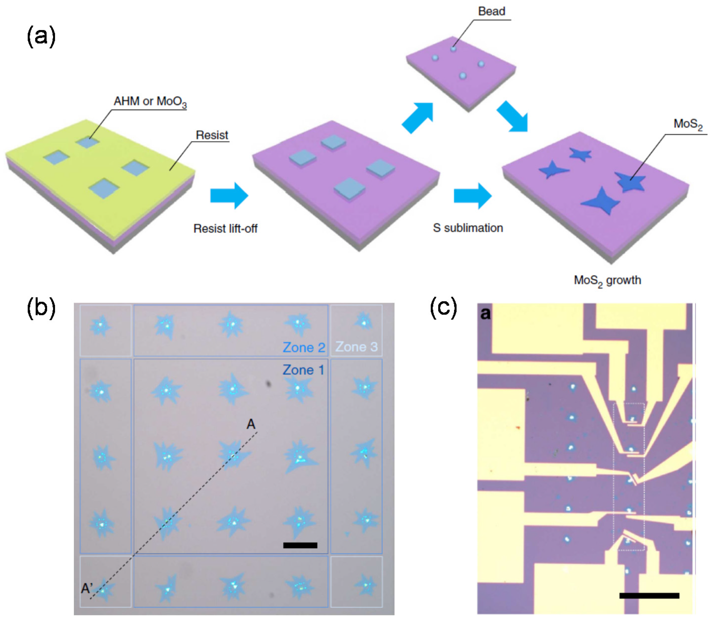
- Han, G.H.; Kybert, N.J.; Naylor, C.H.; Lee, B.S.; Ping, J.; Park, J.H.; Kang, J.; Lee, S.Y.; Lee, Y.H.; Agarwal, R.; et al. Seeded growth of highly crystalline molybdenum disulphide monolayers at controlled locations. Nat. Commun. 2015, 6, 6128. [Google Scholar] [CrossRef] [PubMed]
- Garidis, K.; Jayakumar, G.; Asadollahi, A.; Litta, E.D.; Hellström, P.-E.; Östling, M. Characterization of bonding surface and electrical insulation properties of inter layer dielectrics for 3D monolithic integration. In Proceedings of the IEEE Ultimate Integration on Silicon (EUROSOI-ULIS), Bologna, Italy, 26–28 January 2015; pp. 165–168.
- Kim, S.; Konar, A.; Hwang, W.-S.; Lee, J.H.; Lee, J.; Yang, J.; Jung, C.; Kim, H.; Yoo, J.-B.; Choi, J.-Y.; et al. High-mobility and low-power thin-film transistors based on multilayer MoS2 crystals. Nat. Commun. 2012, 3, 1011. [Google Scholar] [CrossRef] [PubMed]
- Smith, A.D.; Vaziri, S.; Rodriguez, S.; Östling, M.; Lemme, M.C. Wafer scale graphene transfer for back end of the line device integration. In Proceedings of the ULIS 2014—2014 15th International Conference on Ultimate Integration on Silicon, Stockholm, Sweden, 7–9 April 2014; pp. 29–32.
- Vaziri, S.; Smith, A.D.; Lupina, G.; Lemme, M.C.; Östling, M. PDMS-supported Graphene Transfer Using Intermediary Polymer Layers. In Proceedings of the 2014 44th European Solid State Device Research Conference (ESSDERC), Venice, Italy, 22–26 September 2014; pp. 309–312.
- Kataria, S.; Wagner, S.; Ruhkopf, J.; Gahoi, A.; Pandey, H.; Bornemann, R.; Vaziri, S.; Smith, A.D.; Ostling, M.; Lemme, M.C. Chemical vapor deposited graphene: From synthesis to applications. Phys. Status Solidi A 2014, 211, 2439–2449. [Google Scholar] [CrossRef]
- Lupina, G.; Kitzmann, J.; Costina, I.; Lukosius, M.; Wenger, C.; Wolff, A.; Pasternak, I.; Krajewska, A.; Strupinski, W.; Vaziri, S.; et al. Residual Metallic Contamination of Transferred Chemical Vapor Deposited Graphene. ACS Nano 2015, 9, 4776–4785. [Google Scholar] [CrossRef] [PubMed]
- Gao, J.; Zhao, J.; Ding, F. Transition metal surface passivation induced graphene edge reconstruction. J. Am. Chem. Soc. 2012, 134, 6204–6209. [Google Scholar] [CrossRef] [PubMed]
- Gao, J.; Zhang, J.; Liu, H.; Zhang, Q.; Zhao, J. Structures, mobilities, electronic and magnetic properties of point defects in silicene. Nanoscale 2013, 5, 9785–9792. [Google Scholar] [CrossRef] [PubMed]
- Penev, E.S.; Bhowmick, S.; Sadrzadeh, A.; Yakobson, B.I. Polymorphism of Two-Dimensional Boron. Nano Lett. 2012, 12, 2441–2445. [Google Scholar] [CrossRef] [PubMed]
- Gao, J.; Zhao, J. Initial geometries, interaction mechanism and high stability of silicene on Ag(111) surface. Sci. Rep. 2012, 2, 861. [Google Scholar] [CrossRef] [PubMed]
- Gao, J.; Yip, J.; Zhao, J.; Yakobson, B.I.; Ding, F. Graphene nucleation on transition metal surface: Structure transformation and role of the metal step edge. J. Am. Chem. Soc. 2011, 133, 5009–5015. [Google Scholar] [CrossRef] [PubMed]
- Artyukhov, V.I.; Liu, Y.; Yakobson, B.I. Equilibrium at the edge and atomistic mechanisms of graphene growth. Proc. Natl. Acad. Sci. USA 2012, 109, 15136–15140. [Google Scholar] [CrossRef] [PubMed] [Green Version]
- Gao, J.; Ding, F. The structure and stability of magic carbon clusters observed in graphene chemical vapor deposition growth on Ru(0001) and Rh(111) surfaces. Angew. Chem. Int. Ed. Engl. 2014, 53, 14031–14035. [Google Scholar] [CrossRef] [PubMed]
© 2015 by the authors; licensee MDPI, Basel, Switzerland. This article is an open access article distributed under the terms and conditions of the Creative Commons Attribution license (http://creativecommons.org/licenses/by/4.0/).
Share and Cite
Li, J.; Östling, M. Scalable Fabrication of 2D Semiconducting Crystals for Future Electronics. Electronics 2015, 4, 1033-1061. https://doi.org/10.3390/electronics4041033
Li J, Östling M. Scalable Fabrication of 2D Semiconducting Crystals for Future Electronics. Electronics. 2015; 4(4):1033-1061. https://doi.org/10.3390/electronics4041033
Chicago/Turabian StyleLi, Jiantong, and Mikael Östling. 2015. "Scalable Fabrication of 2D Semiconducting Crystals for Future Electronics" Electronics 4, no. 4: 1033-1061. https://doi.org/10.3390/electronics4041033