1. Introduction
Coincidence is a concept that is well understood on a theoretical level. All readers have probably a fair understanding about the coincidence of two events: they simply occur at the same time. However, things dramatically change, if it comes to physical, real-world events. Physical events are always associated with time, which is a continuous parameter by its very nature. Measuring a continuous parameter, such as time, requires some analog-to-digital conversion, which imposes certain quantization errors.
Technically, coincidence is referred to as the occurrence of two events, A and B, that happen within a defined time span, called coincidence window,
Tc. Given the timing information of both events,
tA and
tB, coincidence is indicated when:
The definition in Equation (1) allows for an arbitrary order of both events.
The detection of certain physical events requires a very high resolution-in-time. A good example is the emission of gamma-ray pairs from medical radioisotopes. These radioisotopes are injected into a human body. The detection of a pair of the emitted gamma rays allows for conclusions about a patient’s medical status. For this task, positron emissions tomography (PET) is an approach that detects these rays [
1]. The timing of the detection is crucial for determining the origin of the gamma rays, and subsequent processing stages can reconstruct the position of the event. These post-processing stages are usually implemented in software, and produce colored images that provide information about that specific area of the body.
Since the gamma rays travel with the speed of light, timing requirements are strict. It should be clear that the quality of the resulting image directly depends on the available time resolution, which is about 1 ns or below in state-of-the-art time-of-flight PET systems [
2,
3]. Since these resolutions are still quite challenging for software-based systems, the field of PET systems still enjoys significant activity in the development of hardware-based coincidence detectors. Some of these detection approaches are briefly summarized in
Section 2.
A common characteristic of the approaches reviewed in
Section 2 is that they all employ certain logic gates, e.g., AND gates, as their basic processing elements. It is well known that these gates process input signals based on their actual voltage
levels rather than on signal
transitions.
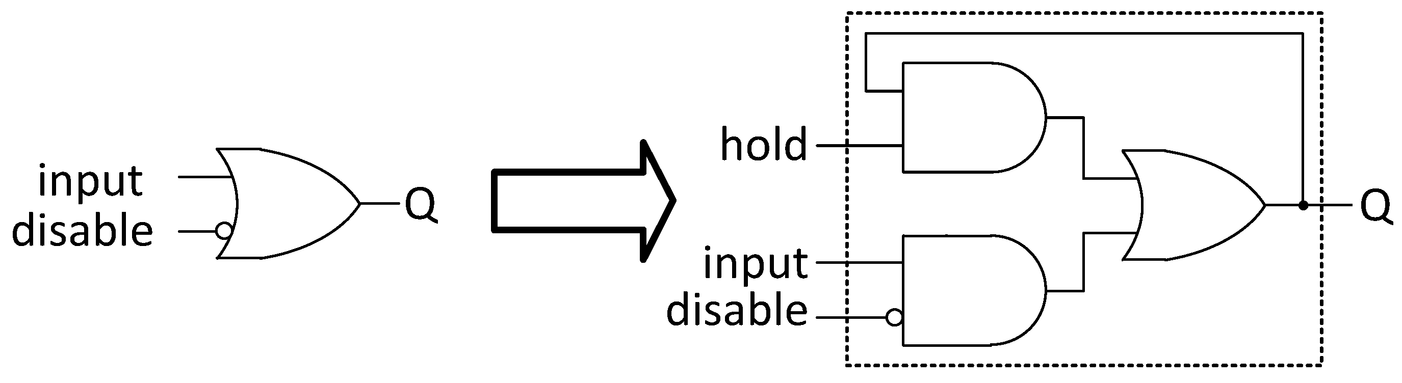
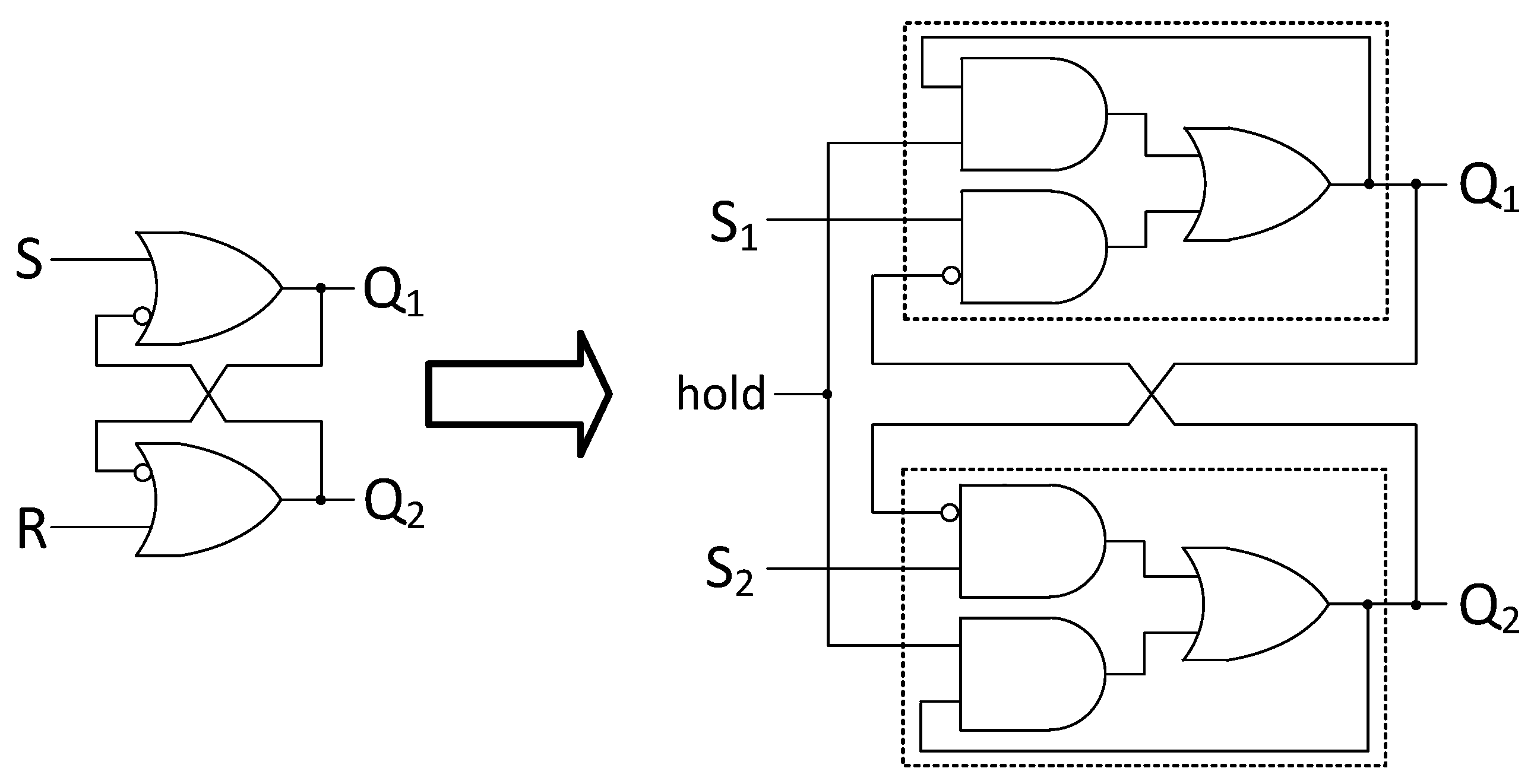
Section 3 proposes a different approach that is based on a new type of RS latch: the latch processes the voltage changes of the input signals and is thus edge-triggered to a certain extend. Thus, it is able to save the edge event rather than losing it like an AND gate that goes low once its inputs go low.
Section 3 illustrates how this special latch structure is able to operate as a coincidence detector with a coincidence window of width
Tc in the range of about a few hundreds of picoseconds. Consequently, this type of latch is called
coincidence detector latch (CDL).
The proposed CDL was implemented in a field-programmable gate array (FPGA) and thoroughly tested in a physical laboratory setup (
i.e.,
not in simulation). All the parameters of the implementation and the test procedure are summarized in
Section 4.
The results are presented in
Section 5 and indicate that the width of the coincidence window is
Tc as small as
Tc ≈ 115 ps, which is at least about ten times smaller (more precise) than reported by other research [
4,
5,
6,
7]. Finally,
Section 6 concludes this paper with a brief discussion.
2. Background
In general, many coincidence detection systems used in medical applications, quantum physics, and optics contain two major parts: single-event detectors and coincidence detectors (see
Figure 1). PET systems, for example, employ scintillation radiation detectors, while certain areas of quantum mechanics research, on the other hand, resort to single photon counting modules (SPCM) that detect emitted photons. The output ports of the detectors provide a signal pulse after the successful detection of an event, i.e
., photon or ray arrival.
Figure 1.
General hardware setup for coincidence detection.
Figure 1.
General hardware setup for coincidence detection.
The second major part of the coincidence detection is a subsequent processing stage that observes the output pulses of the aforementioned detectors. If pulses of two (or more) detectors arrive within an arbitrarily defined time window, the system considers them as coincidental. Recent research has strongly focused on implementing the second processing stage in field-programmable gate arrays (FPGAs), since they are cost-efficient and provide sufficient resources to implement multiple coincidence detectors on a single chip.
The basic method of determining coincidence is of surprisingly low complexity: The incoming events (
i.e., pulses that are emitted by the event detectors) are simply fed into an AND gate [
8]. If two pulses are observed at the same time, the output port of the AND gate is activated. However, this approach faces several limitations. First of all, the length of the event pulses is critical with respect to the length of the coincidence window. Some research [
7] utilized event detectors that provide output pulses of 30 ns. The pulses’ lengths directly determine the coincidence window
Tc. Thus, if one pulse arrives at
t = 0 ns and the second pulse arrives at
t = 28 ns, the AND gate indicates coincidence, even though the actual events that caused the emission of the event pulses are 28 ns apart and the overlay is merely 2 ns.
For many experiments in physics, shorter coincidence windows are required. To overcome the limitations imposed by the external event detectors, others [
4] illustrated a pulse shaping system that shortens the length of the event pulses down to 7.5 ns. In this case, the signal propagation delays inside the FPGA-internal structures were exploited. Pooser
et al. [
7] refer to a pulse shaping approach that includes a digital latch that samples the incoming event pulse. Thus, the coincidence window is limited by the applied clock frequency, which was as high as 400 MHz, resulting in a coincidence window of 2.5 ns.
The systems reviewed above involve synchronously operating subparts, such as digital counters to evaluate the output information from the AND gates. Thus, if pulses from the external event detectors are too short to be synchronously processed, they have to be stretched. In [
6], an incoming event pulse triggers a digital counter to count down to zero. For that count-down time, a high output value is generated as a modified event pulse. Since the counter was driven by a 250 MHz clock signal, the resulting coincidence window is at least 4 ns wide. If switched to double data rate mode in which not only rising clock edges but also falling edges are utilized the coincidence window could be halved to 2 ns.
In summary, state-of-the-art research achieves coincidence windows as short as about 2 ns to 7.5 ns. Since these values are highly coupled to the employed clock frequencies, higher frequencies are required for shorter coincidence windows. Unfortunately, the clock generators (phase-locked loops and delay-locked loops) of currently available FPGAs are limited to about 400 MHz. In order to overcome this intrinsic limitation, the remainder of this paper proposes a new, asynchronously operating coincidence detector.
4. Methods
In order to evaluate the timing characteristics of the CDL, an Altera DE2-70 Development Board serves as a test platform [
9]. The board contains a Cyclone II FPGA that provides 70,000 configurable logic elements. Furthermore, the low-cost development board is equipped with various communication interfaces, memories, and display elements, such as a Seven-Segment-Display, an LCD, and various LEDs. This makes it perfectly suited to host the coincidence detector latch as well as a monitoring system to gather the output of the CDL. A NIOSII soft-core processor served as a monitor system. The processor stored the CDL-output during measurements and transferred it for further processing to a personal computer via a serial RS232 connection.
Beside this processing, the personal computer also controlled the characteristics of the signal generation, which was done by a Keysight 81150A Function Pulse Generator [
10]. The function pulse generator offers an easy-to-use remote programming interface.
The function generator triggers the signal outputs on both channels. The generator’s output signal is a single positive pulse with a width of 200 ns. The rising edge of that pulse is treated as an event in the coincidence detector system. In order to provide different event timings, the function generator applies different user-defined time offsets on every channel. The accuracy of these offsets is limited to ±25 ps according to the data sheet [
10]. Thus, the rising pulse edge on both channels can be set to different points in time. For the remainder of this paper, the event delay Δ
t is calculated as the timing difference between the rising edges of channels 1 and 2 as follows:
Thus, a positive Δ
t indicates that Channel 1 is activated prior to Channel 2, whereas negative values refer to an activation of Channel 2 prior to Channel 1. According to the definition of coincidence in
Section 1, coincidence is given when the absolute value of Δ
t is smaller than the coincidence window
Tc of the CDL.
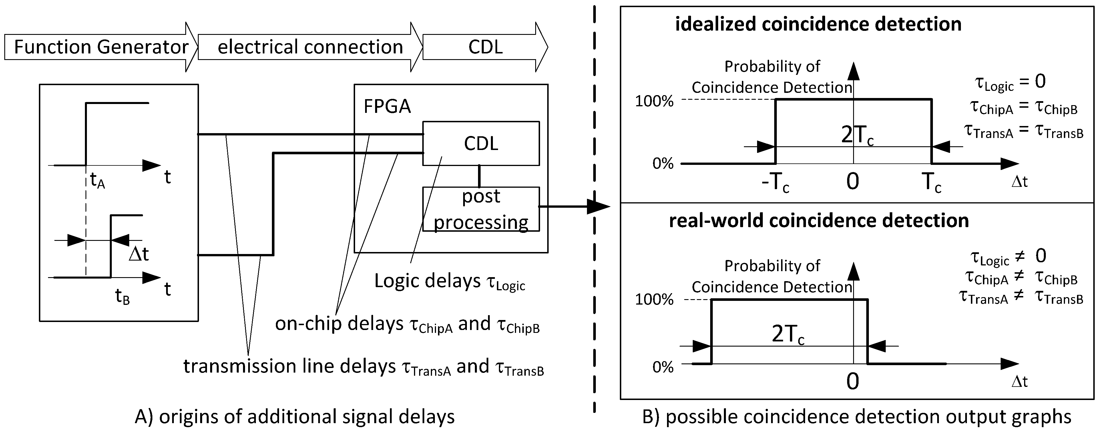
Because of the system layout and its various processing stages, some further remarks should be made in order to help understand the results presented in
Section 5. The actual event timing is given by the signal source (
i.e., the Keysight function generator) at the system input. However, the actual coincidence detection takes place at a certain geometric position
within the FPGA. Due to additional signal paths, drivers, path transistors,
etc., the actual event timing controlled by the function generator differs significantly from the timing observed by a CDL.
According to the coincidence definition in Equation (1), one would expect the CDL to be 100% effective at detecting coincidence from −
Tc < Δ
t < +
Tc. In other words, if one plotted detection efficiency
vs. Δ
t, the plot would look like a square of width 2
Tc centered on Δ
t = 0. This is illustrated in
Figure 6 as the idealized coincidence detection. However, the time of arrival of both signals at the CDL inside the FPGA is highly influenced by architectural signal delays.
Figure 6 illustrates three different origins of timing modification: transmission line delays caused by wires, connectors,
etc.; on-chip delays caused by input pins, drivers, pads, and routing; and logic delays that refer to the structural characteristics of the CDL. For the logic delay, the length of the feedback paths inside the CDL is of special importance. A minor influence might originate from slightly changing technical characteristics of the FPGA’s logic elements, e.g., their specific propagation delays.
Figure 6.
(A) The timing characteristics and the various types of delays; (B) The top panel shows the idealized coincidence detection with no logic delay and equal chip and transmission delays between the two signals. The bottom panel shows a more typical coincidence detection with non-ideal delays.
The combination of these additional delays leads to a shifted coincidence graph. The particular values of the delays depend on the physical location of the logic on the FPGA and therefore differ when the CDL is mapped to different regions within the FPGA.
Taking these additional delays into account, Equation (1) is augmented by a system-based timing offset that incorporates the delay variables shown in
Figure 6:
Equations (3) and (4) describe the real-world (i.e., shifted) coincidence detection plots. The more the additional delays differ, the larger the shift of the coincidence detection plot.
Furthermore, the coincidence window width,
Tc, itself can change with differing delay values. In particular, when the two logic elements that form the CDL are placed at different locations, the lengths of the feedback signals are changed. The longer the distance between those two logic elements, the larger the logic delay, τ
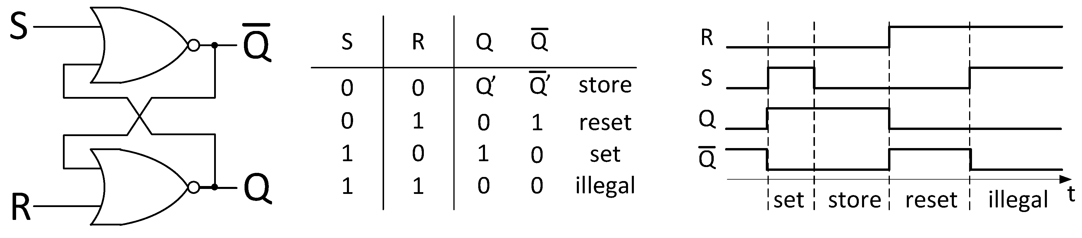
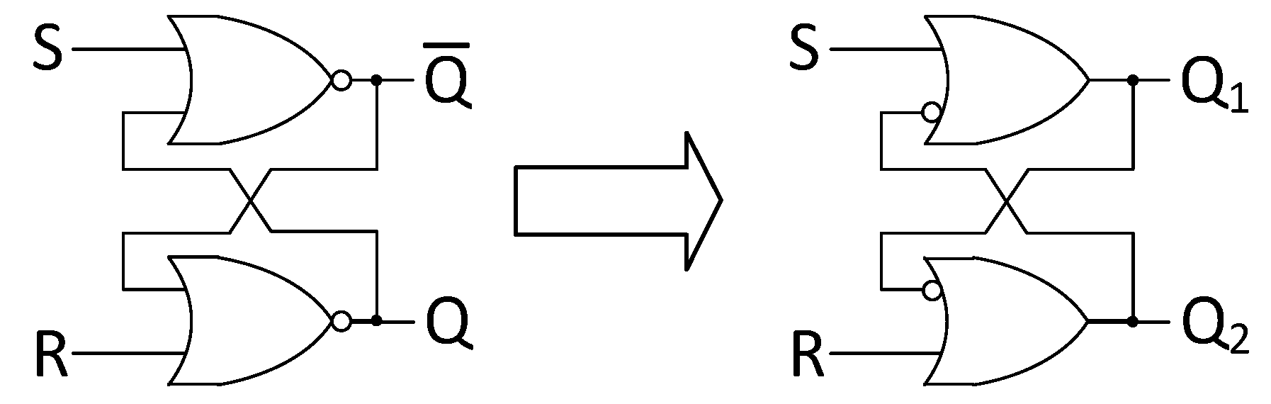
c, is. This is caused by the functional behavior of the RS latch. According to
Figure 5, a signal change on input S
1 activates the output Q
1. The output of one logic element travels along the feedback path to its counterpart. There, Q
1 “locks” the second logic element. If signal S
2 is activated before Q
1 arrives, the CDL states coincidence. Thus, the larger the logic delay τ
Logic, the longer the coincidence window
Tc. The actual width of the coincidence window for different CDL positions is evaluated in
Section 5.
For the experiments, both signal channels were connected to the FPGA development board via the available general purpose input/output (GPIO) pins. To synchronize the signal generation with the CDL-readout, the NIOSII was programmed with the following measurement scheme. First, the processor reset the CDL by deactivating the hold input (see
Figure 5). The hold input is then set again to activate the CDL. In the next step, the processor triggered the function generator to output a pulse on every channel. Finally, the processor read the output state of the CDL. After 1000 measurements, it sent the counted values of the four possible output states {(0,0), (0,1), (1,0), (1,1)} to the personal computer, which in turn wrote them into a file. After a user-defined number of received data sets, the personal computer changed the delay setting.
The coincidence detector latch shown in
Figure 5 was implemented in VHDL. The actual synthesis and routing was automatically done by the software tool chain,
i.e., Altera Quartus II 13.0 SP1 [
11]. The two logic elements forming the CDL were placed in the center of the FPGA in between the logic elements that belong to the NIOS II processor in order to minimize signal path lengths from the CDL to the processor.
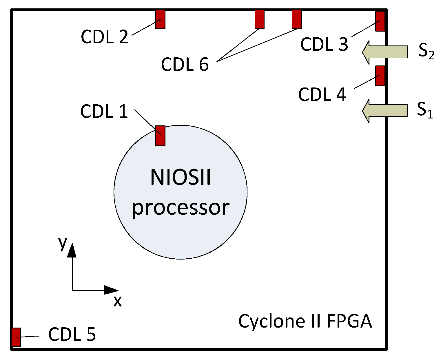
Given that the determination of the coincidence of two events is affected by the path lengths involved, the experimental evaluation also considers different CDL placements on the FPGA device. These alternatives are labeled CDL 2 to CDL 6 in
Figure 6 and resulted in different path lengths. These placements were obtained by manual position assignments in the Quartus project settings file. They were arbitrarily chosen and satisfied the following constraints:
Intermediate distance to the NIOS II processor for noise and cross-talk reduction (CDL 2)
Maximum distance to the NIOS II processor (CDL 3)
shortest path length from the FPGA’s input ports to the CDL’s input ports (CDL 4)
maximum path length from the FPGA’s input ports to the CDL’s input ports (CDL 5)
increasing the cross coupling paths’ length between the CDL’s two logic elements (CDL 6)
Figure 7 also shows the input pads for the two signals S
1 and S
2 that belong to those GPIO pins that are connected to the Keysight function generator. Since the FPGA is mounted on a development board, the options to choose FPGA pins as signal inputs are limited. All pins are hardwired to components on the board. The designer can only chose among those pins that connect to the on-board GPIO pin header.
Figure 7.
Test positions for the CDL on the Cyclone II field-programmable gate array (FPGA). The NIOS II processor and the signal inputs are shown for illustration.
Figure 7.
Test positions for the CDL on the Cyclone II field-programmable gate array (FPGA). The NIOS II processor and the signal inputs are shown for illustration.
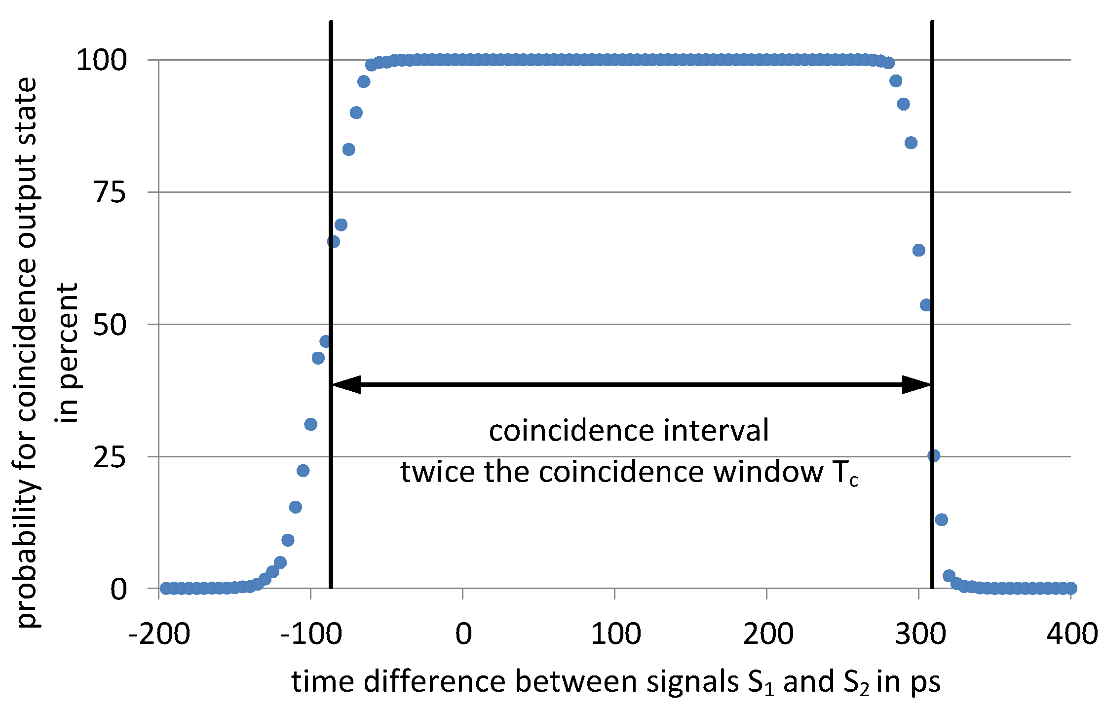
5. Results
The first experimental objective was to provide a proof-of-concept for the functional behavior of the aforementioned CDL structure. The Keysight function generator generated a delay range from −200 ps to 400 ps in steps of 5 ps. At every delay setting, the FPGA evaluated the output of the CDL 1000 times. The result for the automatically placed CDL 1 (see, also,
Figure 7) is shown in
Figure 8.
Figure 8.
Timing behavior of the proof-of-concept implementation of a CDL.
Figure 8.
Timing behavior of the proof-of-concept implementation of a CDL.
As can be seen, starting from an event delay of −140 ps,
i.e., the signal on Channel 2 is emitted 140 ps ahead of the signal on Channel 1, the CDL begins to indicate coincidence in some of the measurements at that particular delay setting. At −90 ps, the 50% level is reached; half of the 1000 measurements indicated coincidence, whereas the remaining 500 measurements did not. The 50% level is marked with the black bars in
Figure 8. From −50 ps on, the CDL stated coincidence in all measurements. This behavior ends at 270 ps, where the output probability for coincidence starts to decrease down to zero. The 50% point is reached at 305 ps; delays larger than 340 ps never lead to coincidence indication. The remainder of this paper defines the duration of the coincidence window
Tc as half of the time between the 50% points. In
Figure 8 this length is
Tc = (305 ps − (−90 ps))/2 ≈ 200 ps.
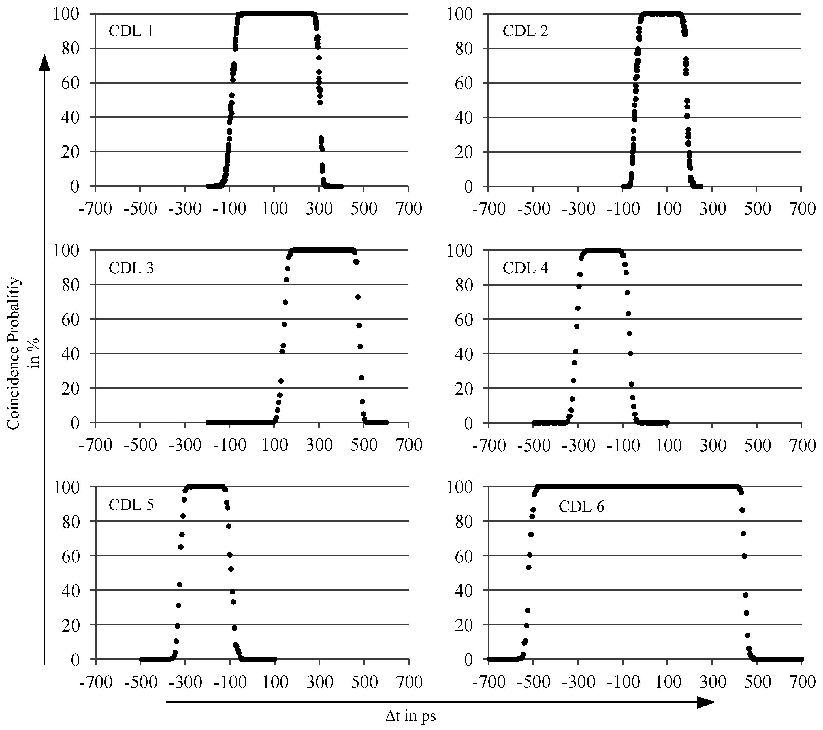
The second set of experiments evaluated five different locations of the CDL within the FPGA. The results for these variants (
i.e., CDL 2 to CDL 6) are summarized in
Figure 9. For illustration purposes, the time axis is identical throughout all graphs. Furthermore, the result for the automatically placed CDL 1 is included for comparison. The measurement range was extended to provide delays −700 ps < Δ
t < 700 ps in steps of 5 ps.
Table 2 provides the detailed measurement results. The three columns
Tc100,
Tc, and
Tcmax state the width of the coincidence window. The subscript indicates the boarders of the coincidence window:
Tc100 only refers to that part of the graph that shows a 100% probability for coincidence detection. The
Tcmax values include all output values greater than zero into the coincidence window calculation. The coincidence window
Tc is based on those output values that show a coincidence detection probability equal to or greater than 50%. The two columns Δ
tmin and Δ
tmax state the lowest and the highest function generator delay setting that caused a positive coincidence detection output. Thus, the term (Δ
tmax − Δ
tmin)/2 provides the value for the maximum coincidence window width
Tcmax.
Figure 9.
Coincidence windows for different setups of the CDL on a Cyclone II FPGA. The time axis for all tests is defined by the Keysight function generator.
Figure 9.
Coincidence windows for different setups of the CDL on a Cyclone II FPGA. The time axis for all tests is defined by the Keysight function generator.
Table 2.
Coincidence window times and timing characteristics of different CDL implementations.
Table 2.
Coincidence window times and timing characteristics of different CDL implementations.
| Name | Tc100 (ps) | Tc (ps) | Tcmax (ps) | Δtmin (ps) | Δtmax (ps) |
|---|
| CDL 1 | 160 | 197.5 | 240 | −140 | 340 |
| CDL 2 | 72.5 | 115 | 157.5 | −85 | 230 |
| CDL 3 | 137.5 | 170 | 207.5 | 100 | 515 |
| CDL 4 | 72.5 | 120 | 165 | −350 | −20 |
| CDL 5 | 75 | 115 | 157.5 | −365 | −50 |
| CDL 6 | 445 | 485 | 525 | −565 | 485 |
As can be seen, the diagrams presented in
Figure 9 are not all symmetric about Δ
t = 0. The reasons for this have already been discussed in
Section 4. CDLs 3 and 4 provide good examples for asymmetric on-chip delays, τ
chip. The length of the signal path from S
1 to CDL 4 is nearly as long as the signal path from signal input S
2 to CDL 4. The center of the coincidence window of CDL 4 is at −185 ps. The path from S
1 to CDL 3 is significantly longer than its path from S
2. Thus, the absolute value of the system timing constant
Tsystem (see Equation (4)) increases and the coincidence window is shifted to the right with the center at +270 ps.
The transmission line delays are unknown. However, they are constant throughout all experiments. Furthermore, the aforementioned CDL 4 is centered at −185 ps, although both of its signal paths do not differ that much in length. This indicates that the transmission lines from the function generator to the FPGA’s input pins have caused this shift.
The width of the coincidence window Tc varies slightly from CDL 1 to CDL 5. The 50% values are in the range of 115–200 ps. CDL 2, 4, and 5 provide especially narrow coincidence windows. On the other end, the coincidence window Tc for CDL 6 is significantly larger.
CDLs 1 to 5 were designed such that their two parts were placed into the very same logic array block which ensures short feedback paths between them. By contrast, the two logic elements of CDL 6 were separated. The logic element that connects to signal S
1 (left part of CDL 6 in
Figure 7) is placed in column 85 of the FPGA, whereas the other logic element (right part of CDL 6 in
Figure 7) is placed in column 90. This heavily affects the system timing constant τ
logic, and thus affects the coincidence window
Tc as announced in
Section 4.
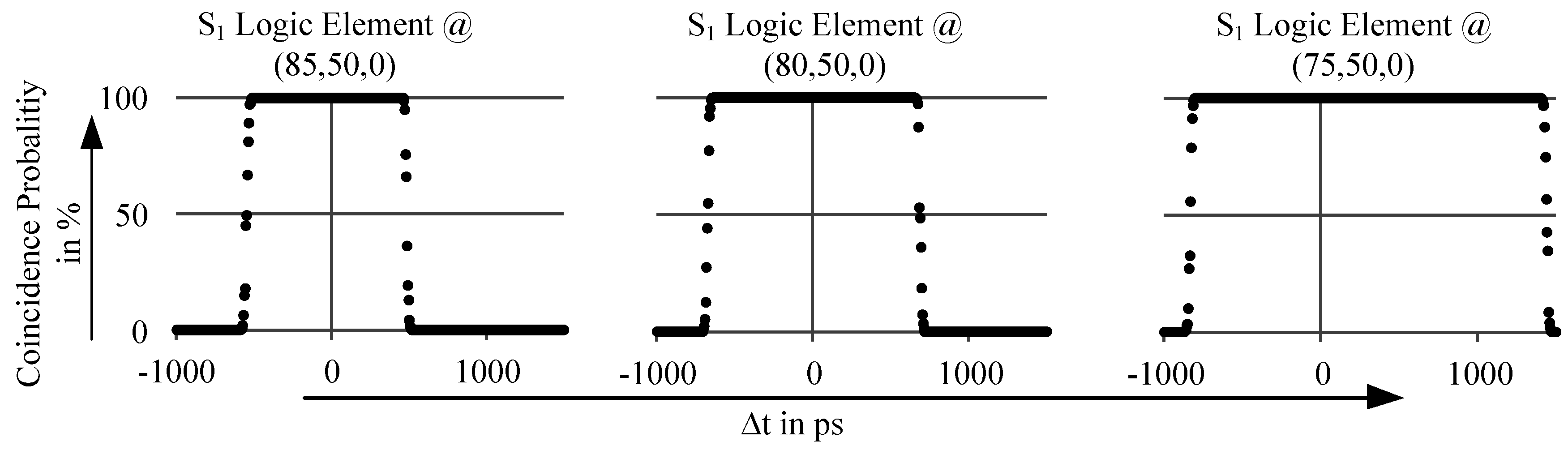
The separation of the two logic elements that form CDL 6 thus provide a design opportunity for arbitrarily formed coincidence windows.
Figure 10 compares the coincidence windows of three variations of CDL 6. The signal input S
2 always connects to a logic element at position (90,50,0) (The coordinate of a logic element comprises: column, row, element number inside the logic array block), whereas the second logic element (that connects to S
1) was placed at positions (85,50,0), (80,50,0), and (75,50,0). Thus, the geometric distances within these three variants were 5, 10, and 15 columns of logic elements inside the FPGA. Transforming these geometric distances into propagation delay values would require exact knowledge about the on-chip structural elements, such as the layout of the utilized routing resources, the characteristics of the involved pass transistors, and the final signal mapping to local and global routing resources. Since this discussion would exceed the scope of this paper by far, a rule-of-thumb would be: Every traversed column of logic elements induces an additional propagation delay of about 50–100 ps.
Figure 10.
Comparison of different feedback path lengths for CDL 6. The S2 logic element resides at position (90,50,0). Thus the feedback path length is 5, 10, 15 columns of logic elements inside the Cyclone IV FPGA (from left to right).
Figure 10.
Comparison of different feedback path lengths for CDL 6. The S2 logic element resides at position (90,50,0). Thus the feedback path length is 5, 10, 15 columns of logic elements inside the Cyclone IV FPGA (from left to right).
Figure 10 shows that the longer the geometric distance between the two logic elements is, the wider their coincidence windows will be. Since the logic element connected to S
1 was moved, the system timing constant,
TSystem, also changed. Thus, the coincidence windows were shifted. As already shown above, a significant elongation of the S
1 signal path leads to a shift in the positive direction. The detailed measurement results are presented in
Table 3.
Table 3.
Coincidence window Tc depending on the distance between the CDL’s logic elements.
Table 3.
Coincidence window Tc depending on the distance between the CDL’s logic elements.
| S1 Logic Element Position | (85,50,0) | (80,50,0) | (75,50,0) |
|---|
| S2 logic element position | (90,50,0) | (90,50,0) | (90,50,0) |
| Feedback path length | 5 columns | 10 columns | 15 columns |
| Center of coincidence window | −30 ps | 10 ps | 300 ps |
| Tc in ps | 485 ps | 680 ps | 1150 ps |
6. Discussion
This paper has proposed a coincidence detection latch “CDL” that provides a promising new option for achieving high-precision, low-cost coincidence detection with coincidence window times shorter than 400 ps. Another appealing aspect is that the hardware structure of the CDL is based on the well-known RS-latch. The CDL can be formed by standard VHDL constructs and is fully synthesizable by common synthesis tools. Despite utilizing six logic gates, it consumes only two logic elements on an off-the-shelf FPGA. Even a vintage Cyclone II FPGA development board could host tens of thousands of CDLs.
The smallest evaluated coincidence window was only 115 ps wide. The experiments indicate that on both ends, the coincidence window has some transient areas where coincidence detection is sporadic. The widths of these areas vary. At the beginning of the window, they usually last for approximately 90 ps to 100 ps. At the end of the window, they are slightly smaller,
i.e., approximately 70 ps to 90 ps. These transient areas might be caused by external effects. The Keysight function generator, for example, provides limited precision during its delay generation. The data sheet states an accuracy of ±25 ps ± 50 ppm [
10]. Furthermore, on-chip as well as on-board noise might be sources of the observed effect. Therefore, the default TTL inputs of the FPGA were driven in LVDS mode to provide better robustness against noise and voltage variation.
When comparing the individual results,
Figure 9 indicates an effect that might be considered a limitation by some: the location of the coincidence window on the
X-axis (the time base) varies among the various CDL implementations. Since the CDL evaluates the signals at its gate inputs, the electrical connections to the CDL’s inputs are part of the
external wiring along with the cables to the function generator. As already illustrated in
Figure 6, this external wiring affects the location of the coincidence window but not the duration of its window. The FGPA synthesis process assigns individual signal routing resources to every CDL. Thus, every particular CDL exhibits an individual coincidence window, with a timing that depends on the physical location on the FPGA device. But this is not a flaw of the developed system, as every timing system has to be calibrated within its actual physical environment.
For experiments that require multi-channel coincidence detection, the use of multiple instances of the CDL on the very same FPGA is possible. Future experiments will investigate this, especially the use of nested multi-channel CDL structures. Furthermore, CDL chains might lead to an even higher time resolution in coincidence detection with the benefit of eliminating the offset limitation discussed above. The experiments indicate that a CDL’s coincidence window Tc and its center point, depends on structural and configurable FPGA parameters. Every single CDL can thus be configured to its required demands. When multiple CDLs are placed on the FPGA, they might be configured in such way that all CDLs evaluate the same signal channel pair. The combination of two CDLs with different center points and overlapping coincidence windows can be used to form a virtual coincidence window that is smaller than a single coincidence window. For example, two CDLs with Tc1 = Tc2 =150 ps and tCenter1 = 0 ps and tCenter2 = 100 ps form a virtual combined coincidence window of Tc = 100 ps and a center point at tCenter = 50 ps. This can be extended for nearly arbitrarily many CDLs.
Unfortunately, it is impossible to calculate precise timing characteristics of a single CDL in advance, i.e., prior to the synthesis process. They depend on a wide variety of parameters. Beside the aforementioned geometric position, also other variables, such as the total number of CDLs, the size and placement of additional control logic, the placement of the input ports, etc., have to be taken into account. Even the very same CDL might behave differently on different FPGAs of the same type. However, the possibility for multiple CDLs operating in parallel might overcome this limitation. The designer can implement hundreds of CDLs, and refer just to those CDLs that provide the desired timing behavior.
In conclusion, this paper has presented a possible approach to design coincidence detectors with a coincidence window of less than 200 ps. Even though the practical experiments were done on an Altera 90 nm Cyclone II FPGA, the results show significant progress towards high precision coincidence detection. The discussion presented above indicates that for a CDL’s final timing characteristics, the involved path delays are more important than the look-up table’s propagation delays. Thus, switching to modern FPGA families, e.g., the 28 nm Cyclone V, might have only minor impacts on a CDL’s overall timing behavior.
Furthermore, the purpose of the practical experiments was to provide a proof-of-concept of the proposed approach. The integration of the proposed CDLs into a commercial system requires, for example, the cooperation with a selected PET system developer, which is beyond the scope of this paper. Nevertheless, such a system integration would include long-term stability tests in order to evaluate the effects of temperature changes, radiation exposure, the event detector precision. It might well be that these long-term stability tests reveal some dependencies, which impose some sporadic re-calibration (e.g., one a week or once a month).


