
Electrical Compact Modeling of Graphene Base Transistors


Abstract
:1. Introduction
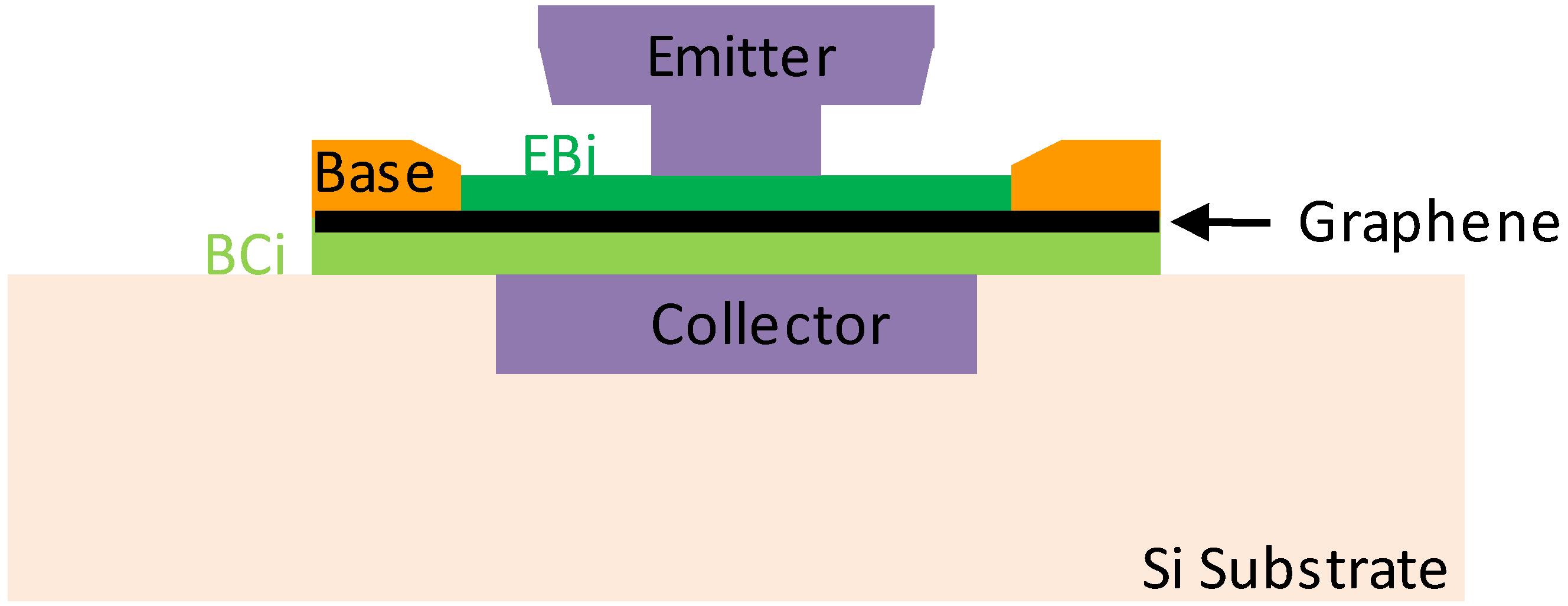
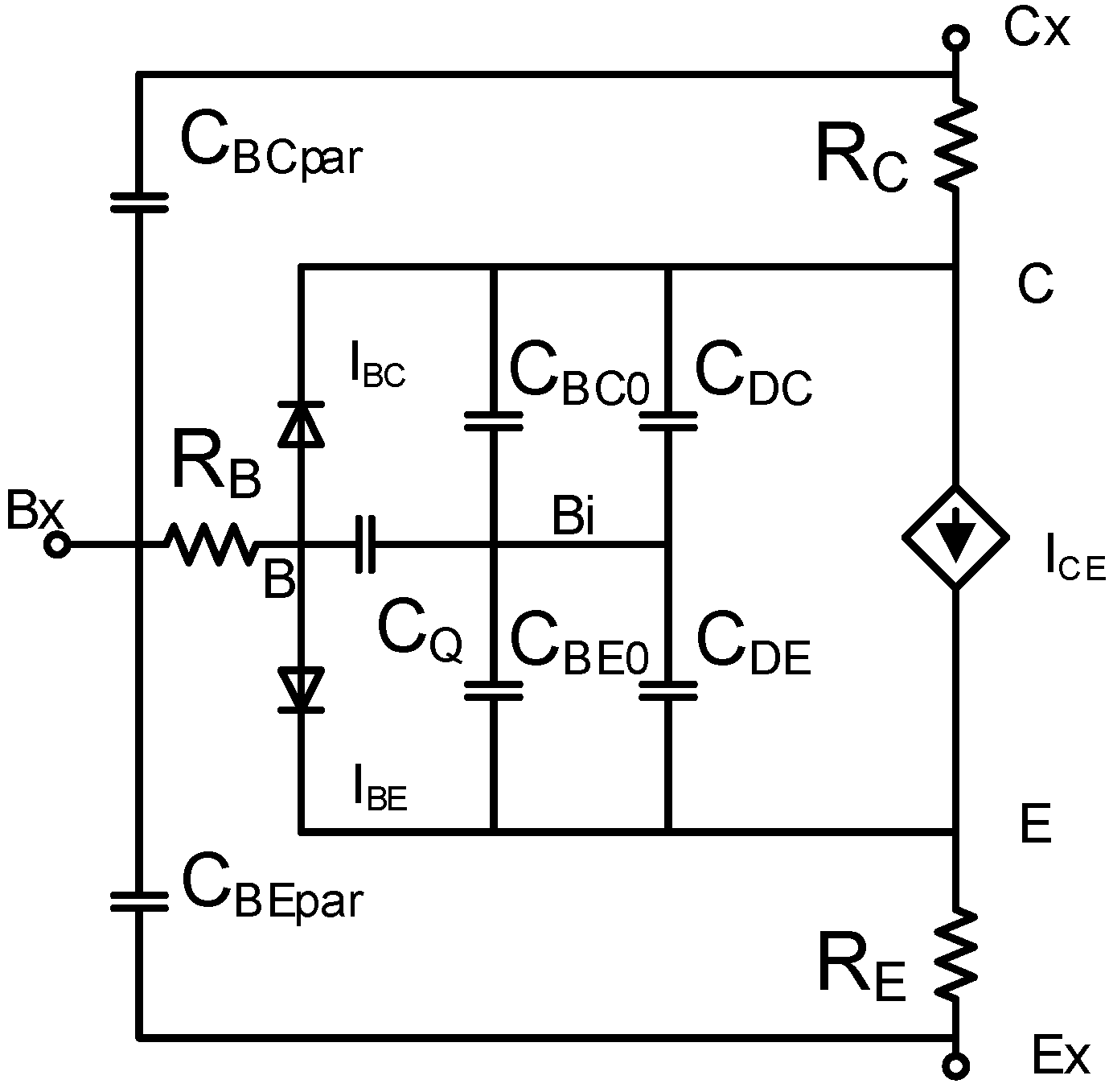
2. Compact Model


2.1. Self-Consistent Calculation of the Internal Base Potential
2.1.1. Description of Diodes and Transfer Current Source
2.1.2. Medium to High Current Injection Effects
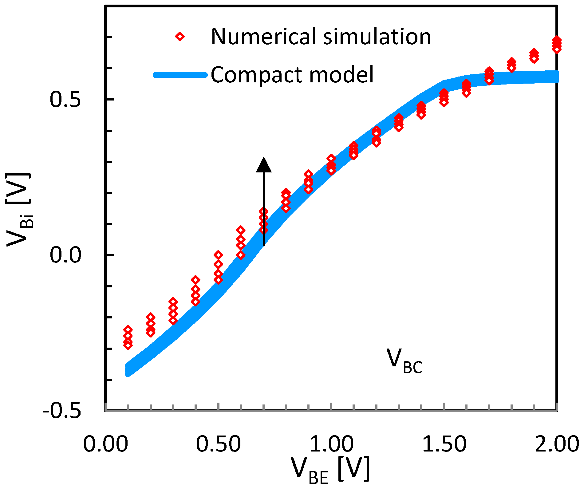
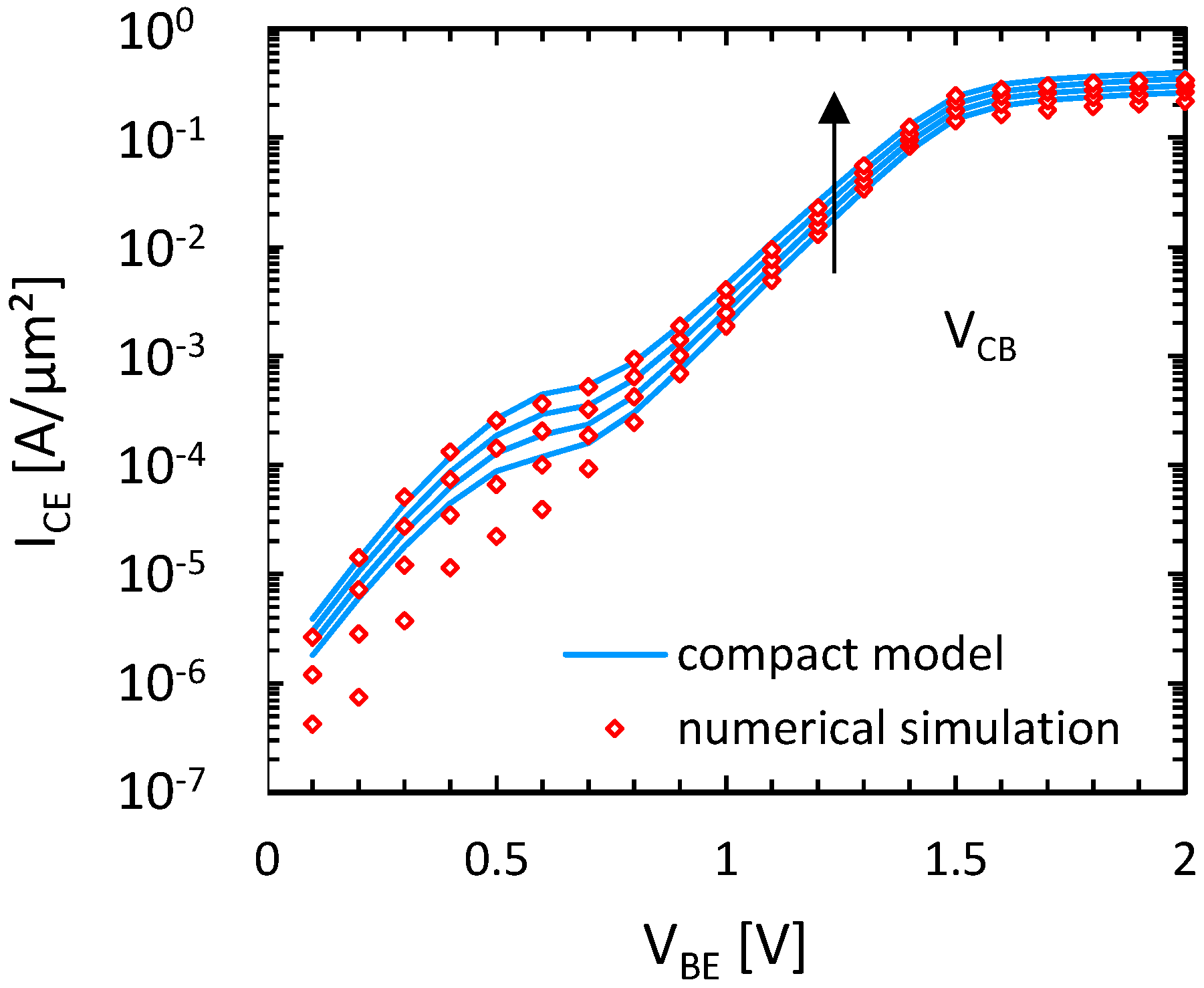
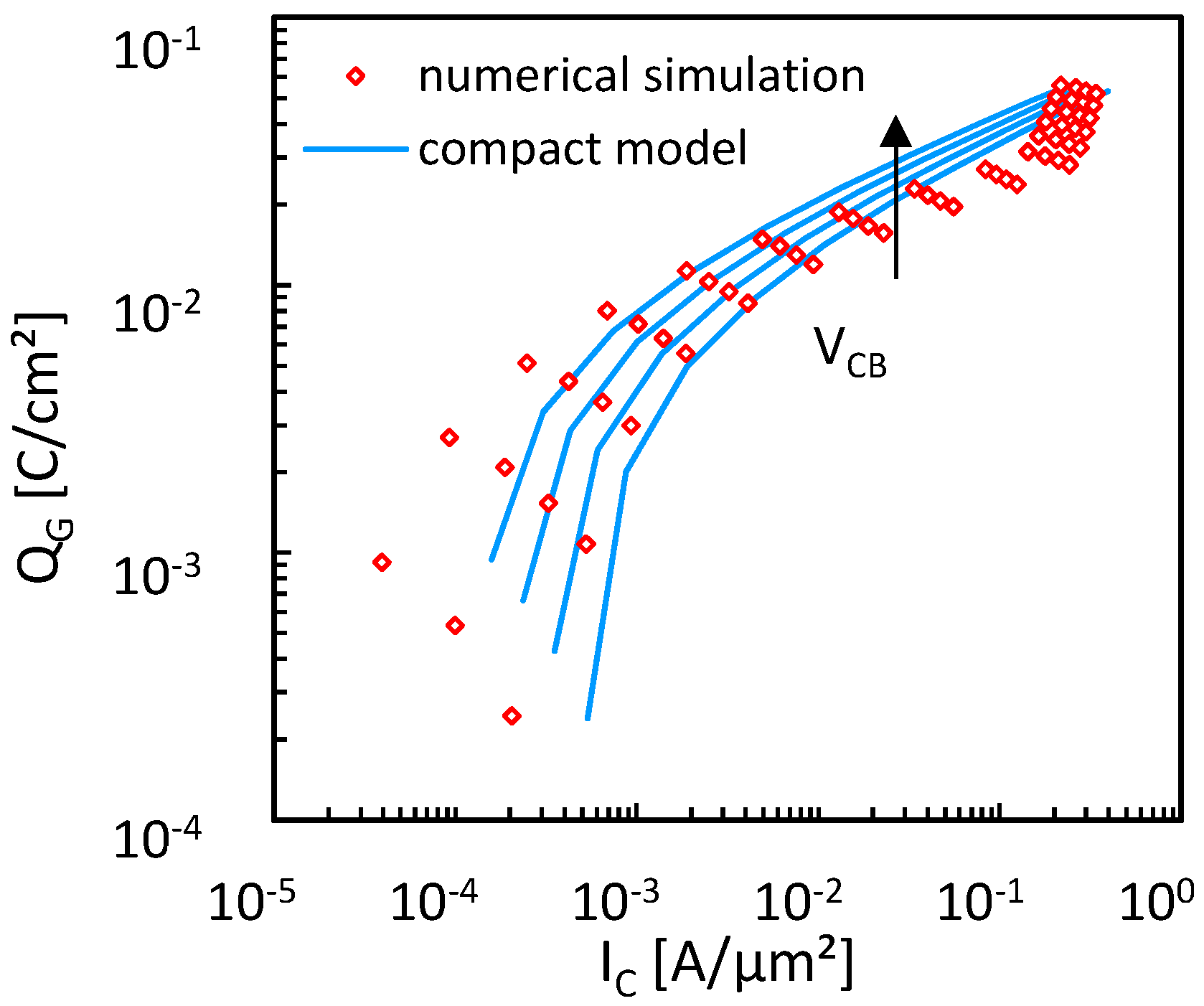
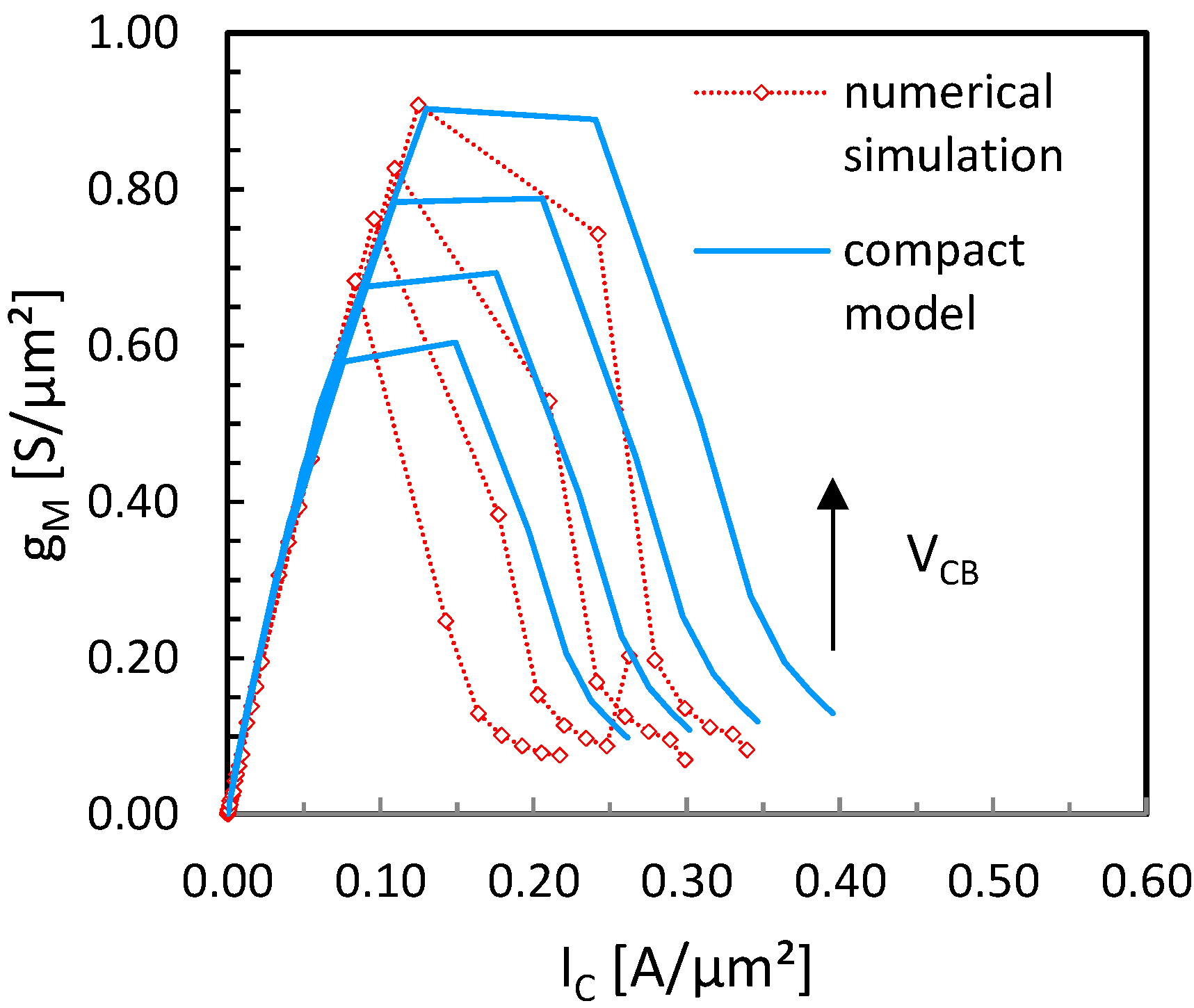
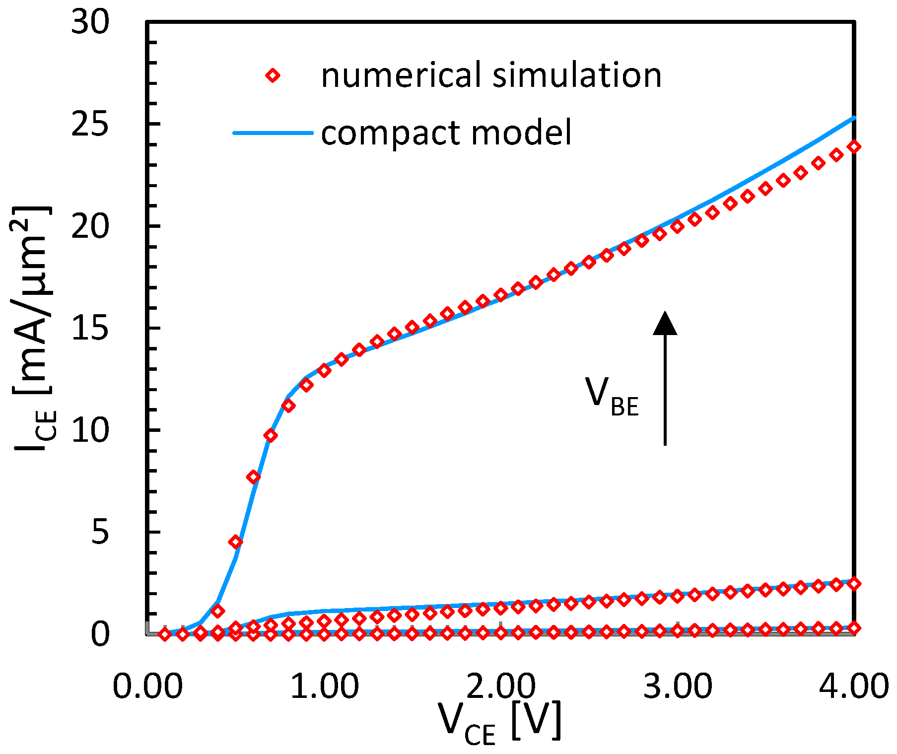
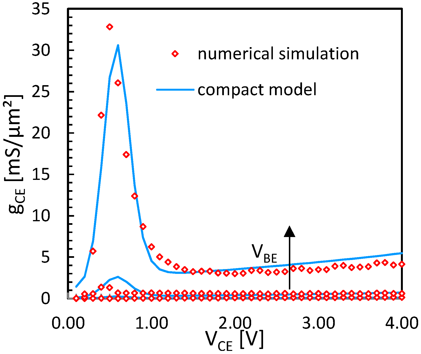
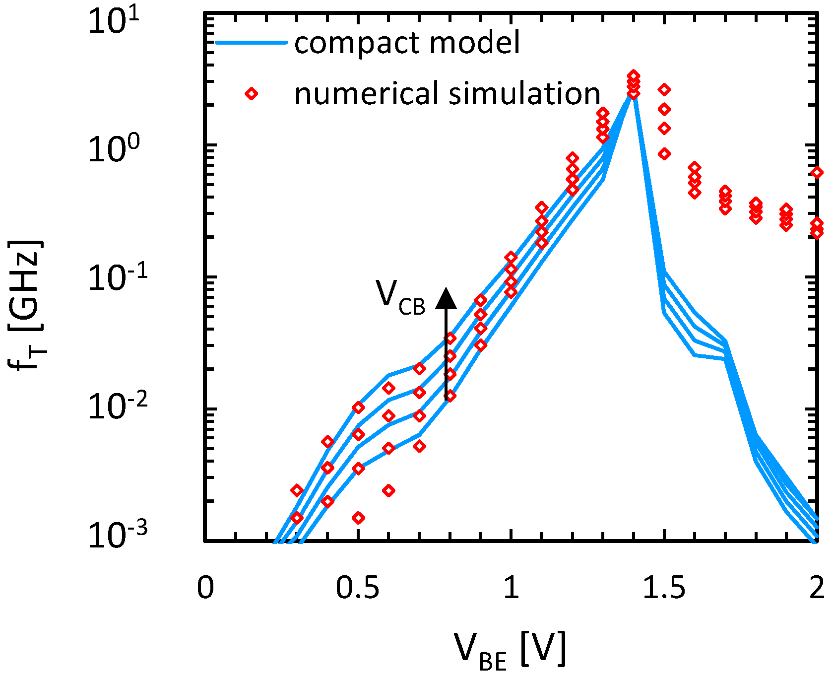
2.2. Comparison to Numerical Simulation


| Parameter Name/Unit | Parameter Value |
|---|---|
| JSF (mA/µm2) | 437 |
| BBE (mV) | 35.3 |
| BBC (mV) | 94.2 |
| ΦCE (V) | 0.57 |
| eBE (nm) | 2 |
| eBC (nm) | 12 |
| εBE | 25 |
| εBC | 2.5 |
| τBE (fs) | 0.35 |
| τBC (fs) | 6 |
| ΦBE (V) | 0.893 |
| ΦBC (V) | 1.2 |
| γ | 1.55 |
| κ (µF/cm²) | 25 |
| ICK (A/µm²) | 0.7 |
| ΔτK (fs) | 8 × 10⁻³ |

3. Conclusions
Acknowledgments
Author Contributions
Conflicts of Interest
References
- Lin, Y.-M.; Farmer, D.B.; Jenkins, K.A.; Wu, Y.; Tedesco, J.; Myers-Ward, R.; Eddy, C.; Gaskill, D.; Dimitrakopoulos, C.; Avouris, P. Enhanced Performance in Epitaxial Graphene FETs with Optimized Channel Morphology. Electron. Device Lett. IEEE 2011, 32, 1343–1345. [Google Scholar] [CrossRef]
- Wu, Y.Q.; Farmer, D.B.; Valdes-Garcia, A.; Zhu, W.J. Record High RF Performance for Epitaxial Graphene Transistors. In Proceedings of the IEEE International on Electron Devices Meeting (IEDM), Washington, DC, USA, 5–7 December 2011.
- Liao, L.; Lin, Y.; Bao, M.; Cheng, R.; Bai, J.; Liu, Y.; Qu, Y.; Wang, K.L.; Huang, Y.; Duan, X.; et al. High-speed graphene transistors with a self-aligned nanowire gate. Nature 2010, 467, 305–308. [Google Scholar] [CrossRef] [PubMed]
- Schwierz, F. Graphene Transistors: Status, Prospects, and Problems. In Proceedings of the IEEE, Ilmenau, Germany, 22 May 2013; Volume 101, pp. 1567–1584.
- Yang, H.; Heo, J.S.; Park, S.; Song, H.J.; Seo, D.H.; Byun, K.-E.; Kim, P.; Yoo1, K.; Chung, H.-J.; Kim, K. Graphene Barristor, a Triode Device with a Gate-Controlled Schottky Barrier. Science 2012, 336, 1140–1143. [Google Scholar] [CrossRef] [PubMed]
- Mehr, W.; Abrowski, J.; Scheytt, C.; Lippert, G.; Xie, Y.-H.; Lemme, M.C.; Ostling, M.; Lupina, G. Vertical graphene base transistor. IEEE Electron Device Lett. 2012, 33, 691–693. [Google Scholar] [CrossRef]
- Vaziri, S.; Lupina, G.; Henke, C.; Smith, A.D.; Östling, M.; Dabrowski, J.; Lippert, G.; Mehr, W.; Lemme, M.C. A Graphene-Based Hot Electron Transistor. Nano Lett. 2013, 13, 1435–1439. [Google Scholar] [CrossRef] [PubMed]
- Vaziri, S.; Belete, M.; Litta, E.D.; Smith, A.D.; Lupina, G.; Lemme, M.; Östling, M. Bilayer Insulator Tunnel Barriers for Graphene-Based Vertical Hot-electron Transistors. Nanoscale 2015, 7, 13096–13104. [Google Scholar] [CrossRef] [PubMed]
- Venica, S.; Driussi, F.; Palestri, P.; Esseni, D.; Vaziri, S.; Selmi, L. Simulation Of DC and RF performance of the graphene base transistor. IEEE Trans. Electron Devices 2014, 61, 2570–2576. [Google Scholar]
- Driussi, F.; Palestri, P.; Selmi, L. Modelling, simulation and design of the vertical Graphene Base Transistor. Microelectron. Eng. 2013, 109, 338–341. [Google Scholar] [CrossRef]
- Venica, S.; Driussi, F.; Palestri, P.; Selmi, L. Graphene Base Transistors with optimized emitter and dielectrics. In Proceedings of the Microelectronics, Electronics and Electronic Technology Conference, Opatija, Croatia, 26–30 May 2014; pp. 39–44.
- Di Lecce, V.; Grassi, R.; Gnudi, A.; Gnani, E.; Reggiani, S.; Baccarani, G. Graphene-base heterojunction transistor: An attractive device for terahertz operation. IEEE Trans. Electron Devices 2013, 60, 4263–4268. [Google Scholar] [CrossRef]
- Xu, H.; Zhang, Z.; Peng, L.-M. Measurements and microscopic model of quantum capacitance in graphene. Appl. Phys. Lett. 2011, 98, 1–3. [Google Scholar] [CrossRef]
- Vaziri, S.; Belete, M.; Litta, E.D.; Smith, A.D.; Lupina, G.; Lemme, M.C.; Östlinga, M. Bilayer insulator tunnel barriers for graphene-based vertical hot-electron transistors. Nanoscale 2015, 7, 13096–13104. [Google Scholar] [CrossRef] [PubMed]
- Ferry, D.K.; Goodnick, S.M. Transport in Nanostructures; Cambridge University Press: Cambridge, UK, 1997. [Google Scholar]
- Zeng, C.; Song, E.B.; Wang, M.; Lee, S.; Torres, C.M.; Tang, J.; Weiller, B.H.; Wang, K.L. Vertical graphene-base hot-electron transistor. Nano Lett. 2013, 13, 1435–1439. [Google Scholar] [CrossRef] [PubMed]
© 2015 by the authors; licensee MDPI, Basel, Switzerland. This article is an open access article distributed under the terms and conditions of the Creative Commons Attribution license (http://creativecommons.org/licenses/by/4.0/).
Share and Cite
Frégonèse, S.; Venica, S.; Driussi, F.; Zimmer, T. Electrical Compact Modeling of Graphene Base Transistors. Electronics 2015, 4, 969-978. https://doi.org/10.3390/electronics4040969
Frégonèse S, Venica S, Driussi F, Zimmer T. Electrical Compact Modeling of Graphene Base Transistors. Electronics. 2015; 4(4):969-978. https://doi.org/10.3390/electronics4040969
Chicago/Turabian StyleFrégonèse, Sébastien, Stefano Venica, Francesco Driussi, and Thomas Zimmer. 2015. "Electrical Compact Modeling of Graphene Base Transistors" Electronics 4, no. 4: 969-978. https://doi.org/10.3390/electronics4040969
APA StyleFrégonèse, S., Venica, S., Driussi, F., & Zimmer, T. (2015). Electrical Compact Modeling of Graphene Base Transistors. Electronics, 4(4), 969-978. https://doi.org/10.3390/electronics4040969