1. Introduction
Nowadays, power electronics are diffused in many applications, covering a wide power range. Electronic converters are commercialized in standard and customized products as compressors, extruders, pumps, fans, grinding mills, rolling mills, conveyors, crushers, blast furnace blowers, gas turbine starters, mixers, mine hoists, reactive power compensation, marine propulsion, high-voltage direct-current (HVDC) transmission, hydro-pumped storage, wind energy conversion, PV generation and railway traction, to name a few [
1].
The multiple degrees of freedom in the control of the electrical parameters allows an electronic converter to optimally regulate voltages and currents that flow through a load, controlling the active and reactive power fluxes and also other parameters depending on the application.
Today, the most popular large variable-speed wind turbines are rated around 1.5–3 MW. Nevertheless larger wind turbines of 10 MW are under development in order to reduce the wind power generation costs [
2].
In the offshore wind case and in many other applications, a high power converter is required, but semiconductor technology has limited capability. To increase the overall power produced by the static converter, many converters have to be connected together. Various connection schemes have been proposed in the literature, such as:
In the first case, many converters are connected in series generating multiple voltage levels with controllable amplitude, frequency and phase. In this way, the voltage of each cell can be kept low, while the total converter configuration can reach a higher voltage level.
In the parallel topologies, two or more converters are paralleled, increasing the total current produced by the inverter and keeping the voltage value constant.
In the hybrid topologies, both series and parallel connections are used in order to combine the advantages of both.
In the parallel solutions, the topology is well defined, and recent studies are focusing on the passive components or the modulation strategies that should be used in order to limit the circulating current between the converters: in [
3], common mode inductors were introduced to avoid this problem, and many other solutions have been proposed in this direction [
4,
5].
In the series solutions, the optimal topology is still not precisely outlined, and many combinations are being studied: the main goal to be reached is a reliable scheme with a low number of switches and multiple voltage levels. Some examples could be the hexagonal topology proposed in [
6], the PackUcell configuration with a crossover switch cell [
7] and the serial modified H-bridge topology prolapsed in [
8]. All of these solutions use different schemes, and the optimal configuration depends on the application requirements.
To make a meaningful comparison between the topologies, many parameters have to be evaluated, such as THD, redundancy and fault tolerance, reliability, costs, the weight and volume of the converter, dynamical behavior, output power, output voltage, switching frequency and losses.
Since in high power applications (P > 5 MW), the electrical inductors and transformers are designed for high currents and voltages, it becomes really important to minimize the filter inductances and to remove the transformers when possible. These goals have to be reached not only because of the costs of the electrical machines, but also because in applications like offshore wind power plants, a reduction of the total structural weight is desirable.
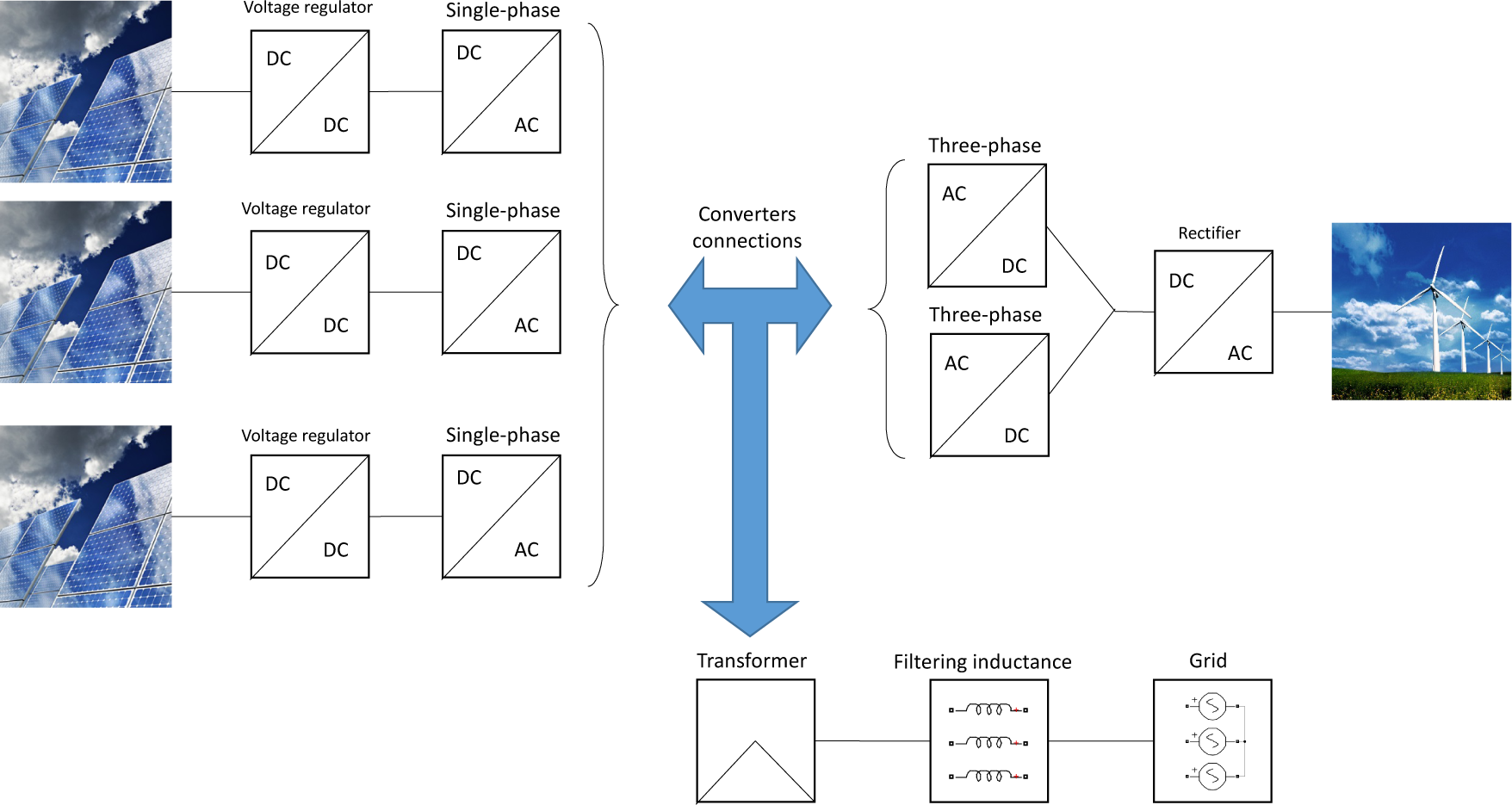
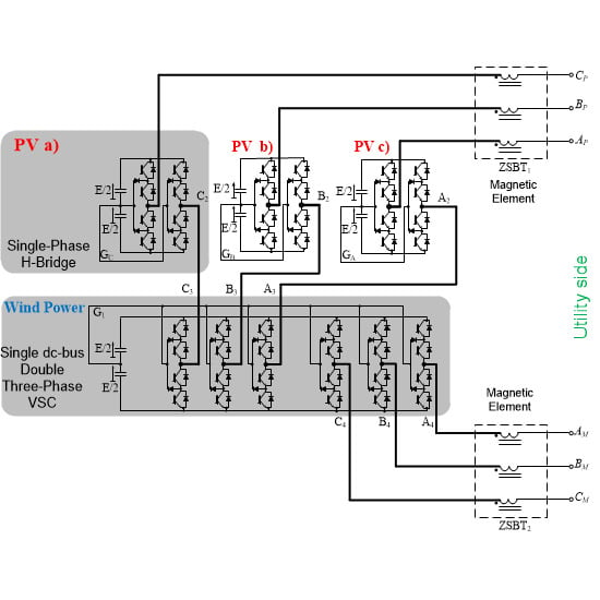
This article will focus on a multilevel topology that uses three single-phase converters and two three-phase converters. Firstly, the control system is presented, and then, the source models and balancing circuits are discussed.
2. System under Investigation
The schematic representation of the topology under investigation is shown in
Figure 1. Three single-phase PV generation systems and two three-phase wind power generators were chosen for this study to show the advantages that the proposed configuration offers as a flexible interface for coupling different energy sources to the electrical network. In
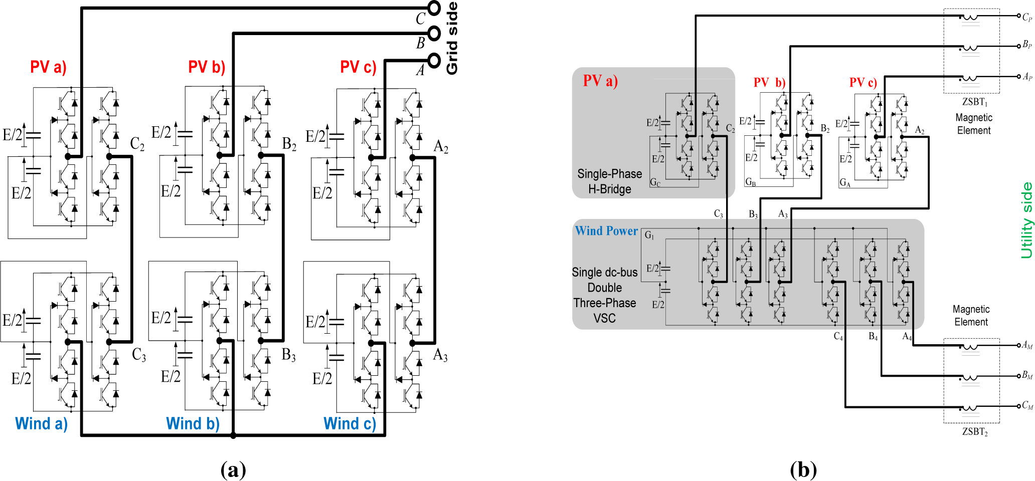
Figure 2a, the classical H-bridge topology that uses six insulated DC buses is reported. The studied configuration visible in
Figure 2b is derived from the previous one: the difference is that two three-phase converters share the same DC bus, and they are connected in series with three single-phase H-bridge cells; the used converters are neutral point clamped (NPC), which is the most diffused multilevel topology. According to [
8], this connection is allowed because of the open-end winding configuration; without this solution, a closedpath for the current would be created (if a special modulation strategy is not developed), and the capacitors would be short-circuited. This means that the open-end winding allows using only four separated buses instead of six.
Furthermore, it is known that in a three-phase converter where the phases share the same DC bus, the instantaneous power is constant in the case of a balanced load. This means that power oscillation at twice the fundamental frequency is not generated, and the ripple associated with the three-phase bus is only due to the switch commutation [
8]. Thus, the size of the capacitors for the three-phase converters can be reduced, obtaining a less expensive solution.
According to [
8], since the open-end winding configuration is adopted, the load imposes zero sequence impedance: if this impedance is low, the zero sequence blocking transformers (ZSBT) must be used to avoid over-currents. For example, if a three-phase three-limb transformer is used, the zero sequence impedance obtained will be low, and the ZSBTs are necessary. If this topology is grid connected through three single-phase transformers, the zero sequence is automatically blocked.
Since the multilevel converters were born to increase the power ratings and the output voltage of the conventional converters, this topology easily fits with medium voltage applications. However, recently, a low voltage application of three-level converters has appeared on the market of wind power plants [
9]; the advantages are the reduction of the filter size, a better harmonic spectrum and the usage of low voltage components that in applications like off-shore wind power plant are desirable.
In this article, the grid voltage will be considered to be Vrms = 1, 000 V with frequency f = 60 Hz.
Considering a fault case in the worst working condition, only one converter will produce power, while the others will be switched off. For example, it can be considered that only one three-phase converter or three half single-phase units (the minimum to guarantee balanced voltages) are working. The voltage produced by a single converter must be sufficient to reach the grid voltage value, considering that the voltage drop on the filter is negligible in comparison with the grid voltage, in order to guarantee a fault-tolerant operation. A commercial IGBT with a maximum peak voltage
Vdc = 1.7 kV is taken as the reference, and therefore, it can be written:
where
Vconv is the phase voltage reached referring to the neutral point;
V dc is the total DC voltage set to
V dc = 2 ·
V max, because in the NPC topology, the switches have only to block half of the DC bus voltage. If the secondary winding is delta connected, the transformer ratio becomes:
The maximum RMS current delivered to the grid and the power are therefore computed fixing the switches’ current limit
Imaxrms = 3, 600 A:
Considering that in the worst condition, one entire converter is able to work, the obtained power is doubled. Using GCTs (gate-commuted thyristors) with a limit peak voltage Vdc = 6 kV, the deliverable power by the topology ensuring fault-tolerant operation raises to P = 22 MW. These results are obtained keeping the converter in the linear modulation region that provides the lowest THD.
In [
8], the sources were considered equal and were modeled with constant voltage sources with equal values. Here, this hypothesis is removed, considering the case of different power sources that can deliver different amounts of power each instant. In this way, this topology can be considered as a hybrid topology, connecting, for example, photovoltaic cells to the single-phase converters and wind power plants to the three-phase converters.
Considering different sources also involves a limit: in this topology, the power delivered by each single-phase converter is proportional to the voltage applied by each converter that must be the same to avoid voltage unbalances. Thus, in the case of failure of one single-phase converter or if null power is produced, the others must adapt to this value, even if they are able to produce. This drawback can be avoided in two ways:
In the former solution, the power is produced by homologous separated sources located in the same region, and therefore, the sources will deliver approximately the same amount of power: considering, for example, photovoltaic cells or wind power plants, the solar irradiation or wind speed can be assumed to be nearly the same in the near areas. If this hypothesis is removed, the power plants must be able to regulate the power delivered, such as the pitch control, in order to obtain the same amount of power always in the single-phase converters. With a smart design of the solar arrays and using additional switches, the power surplus may be addressed to another DC bus (the three-phase DC bus, for example): this smart connection between all of the DC sources would be important in the hypothesis of failure, because it allows recovering the power that normally would be lost.
Since four converters are serialized in this topology, with a proper use of the modulation strategy, the first harmonics band in the voltage output waveform can be shifted by a factor of four, obtaining an apparent switching frequency f = 4 · fswitching, according to the interleaving theory. Thus, the modulation strategy used in each converter is a level shifted carrier pulse width modulation (LS-PWM) with the carriers shifted by ψ = 90°. Because of the arms’ opposite connection in each single-phase converters and in the two three-phase converters, the carriers of the three-phase converters must be in phase with each other and phase-shifted relatively to the carries of the single-phase converters, again in phase with each other. This is valid considering that all of the sources have the same DC voltage. Because of the serial connection, the current is the same, and the condition on the power becomes P singletot = P threetot; this means that the power produced by a single single-phase DC source must be
. If this link is removed, the harmonic cancellation will not be perfect, because the voltage phasors applied by three-phase and mono-phase converters will be different. This means that generally, the switching frequency band appears in the voltage waveform centered at 2 · fswitching; changing the power ratios, the reduction of the harmonic band centered at 2 · fswitching will be variable, and a theoretical perfect elimination will be possible with the total power ratios nearly equal to one.
According to [
10], power converters suffer from power oscillations and over-currents when the AC source becomes unbalanced, and many methods that control the positive and negative sequence have been proposed. In the case of a distorted AC source due to grid faults or disturbances, the unbalanced AC voltages have been proven to be one of the greatest challenges for the control of the converters in order to keep them normally operating and connected to the source.
Since in the selected topology, a closed path for the zero current is created, this current can be controlled in order to obtain specific objectives when an unbalanced fault appears on the grid side. In the studied topology (
Figure 2b), the control of the negative and zero sequence can be activated when an unbalance fault is detected on the single-phase converters, while the three-phase converters deliver active power. When the unbalance is removed, the control of the single-phase converters can be changed again to the positive sequence.
3. Control System Design
In this study, the first hypothesis done was to have a DC input voltage regulated by the DC controllers outside of this topology: for example, for the wind power production plant or when generally the production is in AC, the rectifier can be set to control the DC voltage. If a direct DC source is used, the DC voltage can be regulated using a DC-DC chopper. In this way, active and reactive power exchanged with the grid are controlled directly.
The classical approach with inner current loops and outer power loops driven by the capacitor voltages cannot be used, because many capacitors must be controlled; therefore, another approach has been followed. Through measurements depending on the power plant, the active power that can be delivered by single-phase converters and three-phase converters is known. Through an optimization counting all of the constraints given by the switches and additional constraints, the solution that optimizes the power delivered to the grid is found. This solution consist of the single-phase and three-phase voltage phasors that should be applied and also the power itself, which may be different from the power produced by the DC sources. In this way, the general control structure can be used: from the optimization, the reference values of the total active and reactive powers are known. The reference values of id and iq are computed using a PI (proportional integral controller) for the active power and another for the reactive power. The current values are used in two separate current loops that produce as a result the values of the overall converter voltage phasor, given by the sum of the single-phase and three-phase contributions. The module and the angle of this phasor are known (δ, referring to the grid phasor). To divide the contributions of the single-phase and three-phase phasors, the result of the optimization is used. In fact, according to the optimizer algorithm, the total power reference is calculated starting from the DC available power; the voltages applied by the converters will be unknowns in this process (because of the link between voltages and powers), and for any combination of input DC powers, the total power together with the voltages applied by all of the converters are found. From the knowledge of the absolute voltage values, the relative percentage contribution of the single-phase converter and three-phase converter may be computed referring to the total voltage that the converter should apply.
This solution allows one to use only four controllers with linear transfer functions. The weakness is that the system has to rely on the optimizer algorithm, which may not have convergence (but this will be visible from the look-up table plots), or can estimate quantities based on wrong inputs if, for example, the total impedance changes because of a fault or any other change in the system.
4. Optimization of Power Delivered to the Grid
In a simple case, the problem could be solved analytically: the minimum value of the single-phase powers is taken as single-phase reference; then the single-phase power is added to the three-phase reference, and the total power is found. To deliver the maximum power to the grid, the reactive component of the current that flows through the switches should be equal to zero, which is equivalent to the condition cos(
ϕ) = 1. The current expression becomes:
where
Pm and
Pt are the single and three-phase powers associated with only one converter (one arm of the single-phase and one three-phase converter). Considering that the connection impedance parameters are known, the total voltage drop phasor on this impedance can be calculated, and finally, the components of the converter voltage (phase
δ and amplitude) are known. Finally, the voltage values for each converter can be calculated as:
where
Vm and
Vt are the voltages due to one arm of the single-phase converters and of the three-phase converters referring to the neutral point. The objective function that the optimizer must maximize is:
where the variables of the optimization are:
Vm and
Vt are the mono- and three-phase voltage amplitudes;
I is the current module;
ϕ is the angle between the grid voltage and current phasors;
δ is the angle between the converter voltage phasor and grid voltage phasor;
Pm and
Pt are the active powers delivered by each converter. The angle
ϕ is kept as variable in order to allow the converter to help the grid voltage regulation. For this function, additional conditions must be considered, and in order to keep the problem simple in this analysis,
ϕ is equal to zero (a condition that has to be removed obviously if
ϕ ≠ 0). The constraints that the solver must take into account are divided into equality and inequality constraints:
Pmlim and
Ptlim are power limits known by environmental measurement;
Ilim, Vlim are the switches limits, and the grid voltage is reported to the converter side through the turns ratio of the transformer.
δ obviously must be positive, and the conditions on
ϕ is dependent on the system: if a frequency and voltage dropfunction must be implemented, the standard limits on power factor can be chosen according to IEEE standards (for example, cos(
ϕ) > 0.85 lagging or leading for solar PV systems, IEEE 929).
Since the voltage applied by each converter is an optimization output, the DC voltage reference in all of the sources is changed according to the power produced in order to keep a high modulation index and an output concatenated voltage waveform of each converter with five levels.
The optimized results are stored in look-up tables, and the input variables in the studied simple case are Pm and Pt. The transformer rated power can be chosen to be lower than the maximum power produced by all of the sources if the probability to have the maximum generation of all of the sources at the same instant is low; this allows for a cost reduction.
4.1. Additional Controllers
In order to avoid initial current spikes in the in-rush transient, the power loops are blocked to zero during the initial operation when the PLL (phase locked loop) still has to track the grid signal. The key issue during fault operation of a converter is to guarantee the protection of the converter itself. With the control structure adopted, if a three-phase fault or a voltage dip occurs and if the look-up tables are two-dimensional (input
Pm and
Pt without
Vgrid), the power loops are not able to see the equivalent impedance change or the grid voltage dip, and the power reference will remain the same. Since the impedance during a fault is lower, the power reference can be reached with an increasing of the current. The solution would be a simple saturation of the
Id and
Iq reference values to 1 p.u., but in this hypothesis, if the inverter is injecting both active and reactive currents, the limits would be reached satisfying the single conditions on
Id and
Iq. As explained in [
11], this problem can be solved using a dynamic current limiting control. In the normal operation, the current limits are
Id = 1 and
Iq = 1. When a fault is detected on the grid (voltage dip, three-phase short circuit or other disturbances), a script is run. If the total current
Irms is bigger than the limit, the instantaneous
Id value is memorized, and
is computed. These two parameters are set as new saturation limits, and they will remain unchanged till the fault is removed. When the disturbing action ends, the initial limits are restored. In this way, if the entire converter were delivering the current
Id and the reactive current
Iq to give voltage assistance to the grid before the fault, after the fault, the values of
Id and
Iq will remain unchanged (if the transient is neglected), while the powers will change according to the impedance change (or voltage dip).
4.2. Source Models
The simplest source model that can be considered is a constant voltage generator: this situation is far from the real operation (it would require an infinite capacity). The DC sources are therefore modeled with capacitors designed imposing a certain ripple limit. Using the equation proposed in [
8], here reported:
it is easy to see that the first current harmonic with frequency 2·
f = 2·60 = 120 Hz requires a capacitor to limit the ripple to 10%:
In
Equations (12) and
(13), the modulation index has been fixed to one, the rmscurrent in the AC side is
I = 2 kA (the maximum), the DC voltage has been fixed to
VDC = 1 kV and the current derived by the neutral point is neglected, since its frequency will be much higher than
f = 120 Hz. The resultant capacitance is the series of upper and lower capacitance. One of the hypothesis behind
Equation (11) was to fix
ϕ ≃ 90°, which is verified if the converter injects mostly reactive power into the grid. Therefore, the single capacities will be:
Cm−single = 2 ·
Cm = 37.52 mF.
Regarding the three-phase converters, the single capacity is studied because the neutral current is not negligible (the switching frequency is involved).
where
Im is the rms value of the current harmonic with the switching frequency,
ωhf is the angular speed associated with the switching frequency and
and
Ct−single are the voltage and the capacitance of a single capacitor. Since the voltage on the capacitor is regulated by an external controller, one
PI (proportional integral regulator) for each DC source is used in order to model the delay and the overshoot of the voltage regulator. The expressions in the open and closed loop, including the PI regulator, are:
where
K is the PI proportional term,
T is the PI time constant and
C is the total capacitance (sum of the upper and lower ones). The time response applying a unitary step to the voltage reference is found applying the Laplace anti-transform:
The proportional gain is inversely proportional to the time constant of the power regulation, where
. If the power regulation is related to a mechanical process, this time constant will be low. The second parameter to be designed is the time constant T of the PI, using the capacitance values found in
Equations (13) and
(15).
In this way, the operation of the sources is simplified: the power associated with each DC source is known together with the voltage reference that should be imposed on the DC bus. The PI controller controls the voltage injecting a current into the capacitors, and the saturation limit is fixed as the ratio
. The scheme is depicted in
Figure 3; it assumes that the power absorbed by the DC source is regulated according to the voltage requirement, giving a variable voltage as the output (with a certain delay); the simplified model allows one to obtain a light simulation without implementing an MPPT algorithm (maximum point power tracking).
4.3. Real Implementation
In the real case, the MPPT module should be implemented for all of the DC sources in order to optimize the power production, while DC-DC choppers must be used in order to adapt the voltage level from the source level to the reference level. For the single-phase sources, MPPT algorithms must also be able to reduce the converted power when the single-phase available powers and DC voltages are not equal to each other. Normally, the power mismatch should be limited, and therefore, the single-phase MPPTs have to work near the maximum power point; if the power mismatch is relevant, the MPPTs are also able to work in this condition.
For the three-phase source, the MPPT algorithm achieves the maximum power conversion; therefore, the MPPT implementation is simpler than the single-phase case.
According to the optimizer structure, the power injected by each converter is equal to the one associated with the respective DC bus in normal conditions (neglecting transients on the capacitors and errors on the power measures). This means that the capacitors should be naturally balanced. In practice, the transients must be taken into account, and the scheme topology could be modified in order to control also the voltage of the DC bus. Additional PIs could control the DC buses voltage error giving as output coefficients in the range (0.95–1.05), which will multiply the input power of the optimizer: when the DC voltage goes below the reference, the power reference of the converter will be decreased (and vice-versa), while the power converted from the source is fixed by the MPPT. In this way, the additional energy produced by the sources will be stored in the capacitor, increasing its voltage. The corrective parameter has a small range in order to not compromise the loop stability.
The proposed solution has to be verified and will be part of future work: in particular, the MPPTs’ operation, the stability of the feed forward and the case of unbalanced single-phase DC buses have to be discussed and verified through simulations and experiments.
4.4. Neutral Point Balance
It is well known that the NPC topology suffers from DC voltage balancing. While the sum of the voltages of the capacitors is controlled by the external source (current generator loops), the voltage distribution between each component is not controlled. This causes asymmetries on the voltage output on the AC side and leads to unstable operation. According to [
12], the different voltage values can also lead to premature failure of the switching devices, and the THD of the output current increases because low-order harmonics appear and become dominant. Many techniques have been proposed in the literature to deal with the unbalanced operational behavior. Some techniques use a modified switching pattern in order to use the states’ resonances to control the voltage sharing between the capacitors. Other techniques use an additional external circuit with additional switches and components to control the voltage balance. In [
13], a very suitable balancing method is proposed. This technique is based on voltage injection for single-phase three-level converters when the carrier-based modulation is used. This method has been implemented in all of the single-phase converters.
The biggest problem to be solved is the one related to the three-phase balance. In [
14], another algorithm based on the zero sequence voltage injection where the zero sequence current is controlled is presented; however, this scheme in the studied topology should take into account the zero sequence voltage applied by the single-phase converters, centered at 2
· fswitching, and this high frequency voltage would saturate the PI of the proposed scheme. An interesting solution is proposed by [
15] for parallel configurations, where the voltage balancing is obtained through a resonant
RLC circuit. In this paper, it is explained that when a voltage unbalance occurs, the output voltage waveform changes its harmonic spectrum, because the switching frequency appears, while normally, it should be canceled because of the unipolar operation, seen as interleaving. In this work, a three-phase RLC circuit has been used as a filter tuned on this frequency, providing the balancing effect.
5. Simulation Results and Discussion
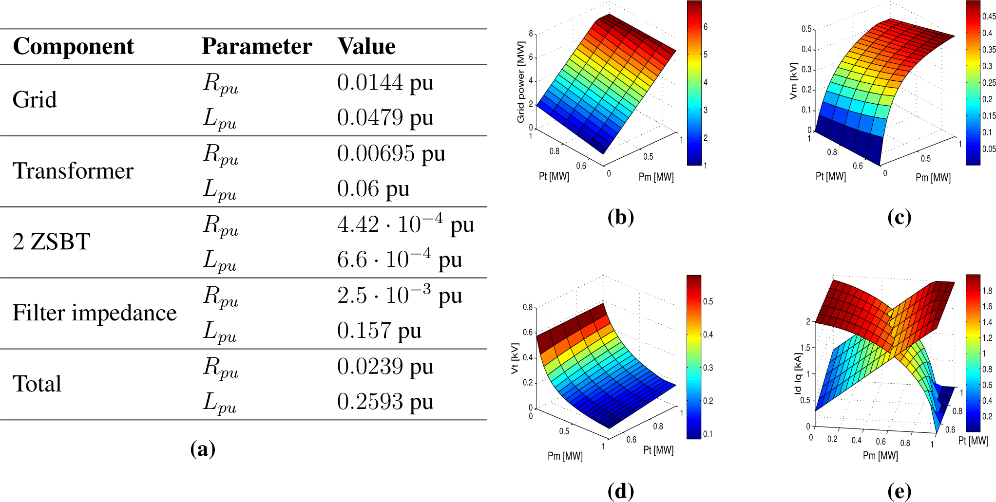
In Table
4a, the values used in the simulations have been reported as per unit system. In
Figure 4b,c,d,e, the optimization results have been depicted considering a power range for the single-phase and three-phase powers
P m = [0, 0.05,
…1] MW and
P t = [0.5, 0.55,
…1] MW, respectively, a transformer ratio
k = 0.5 with wye connection on the grid side and a limit current on the converter side
Imax = 2 kA, equal to
Ilim = 4 kA on the grid side. These results are implemented in look-up tables.
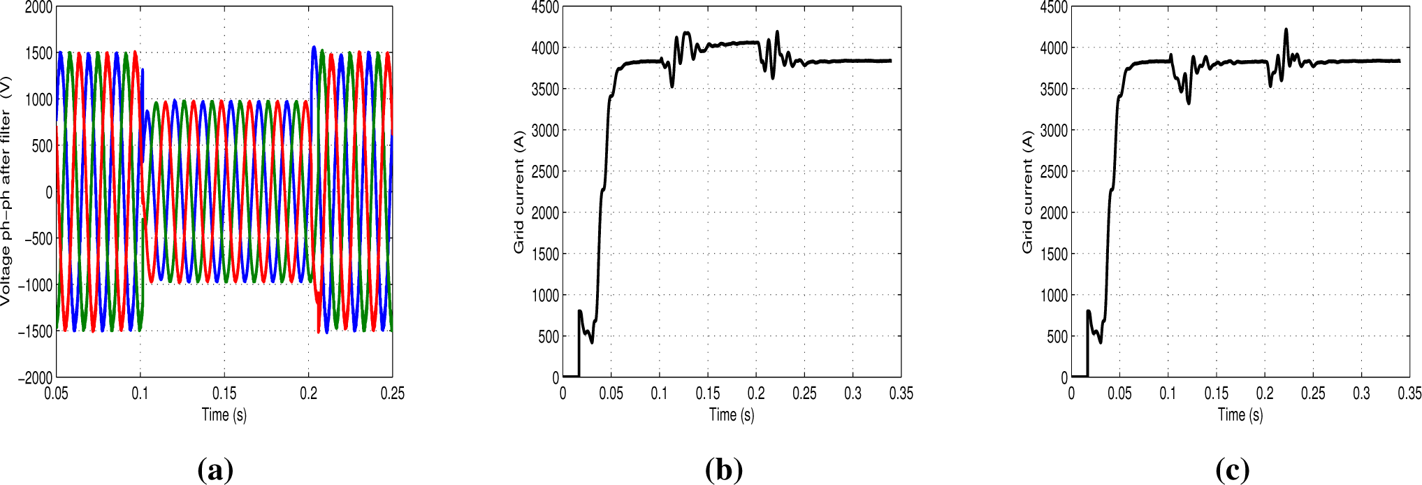
In
Figure 5, the operational behavior of the converter is shown when a voltage dip occurs, while the converter is delivering active and reactive power to the grid: without the dynamic limit, the current exceeds the maximum value, while with the proposed circuit, it remains below (neglecting the transients).
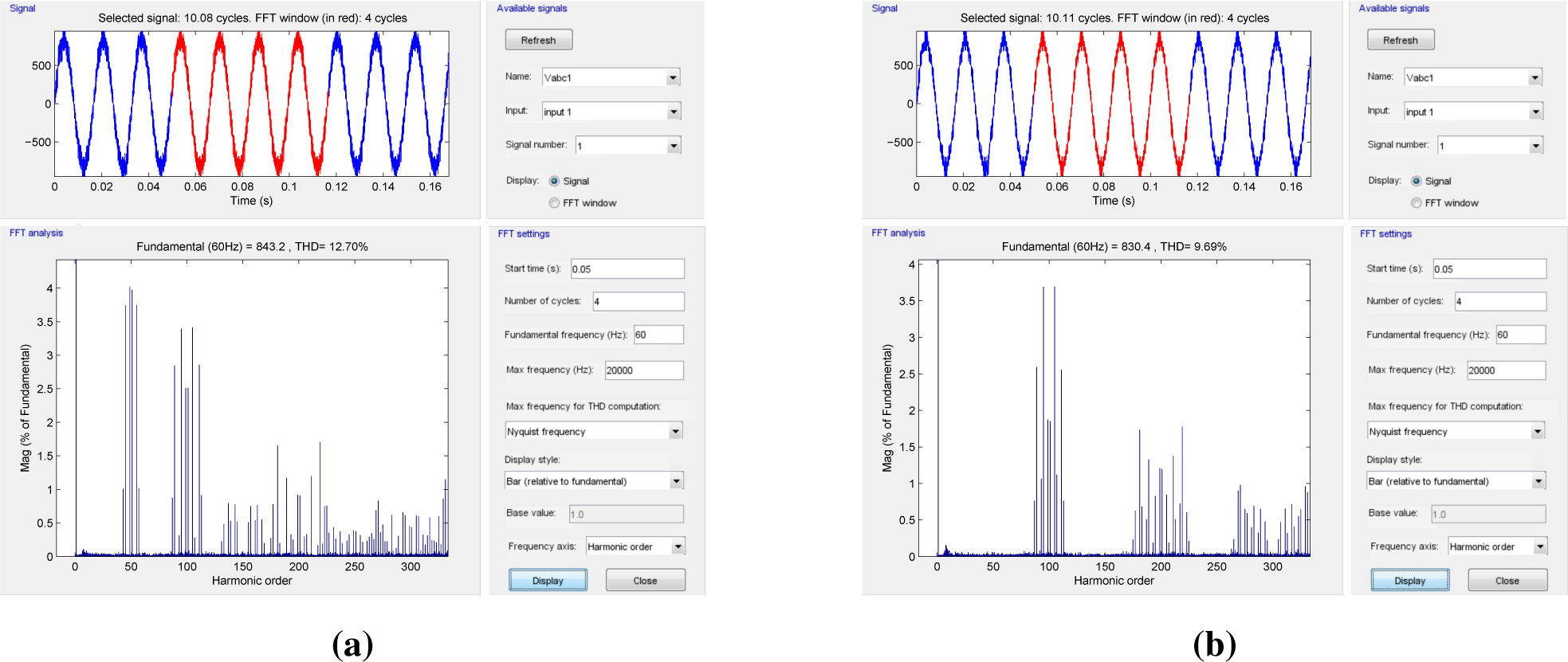
In
Figure 6, the FFT analysis of the voltage measured between the power transformer and the filtering impedance and referring to the ground is reported; in
Figure 6a, the power sharing among single and three-phase converters is far from the optimal one, and the first harmonic band is centered at
f = 2
fswitching; while in
Figure 6b, the optimal power ratio is achieved, and the first harmonic band is centered at
f = 4
fswitching. In
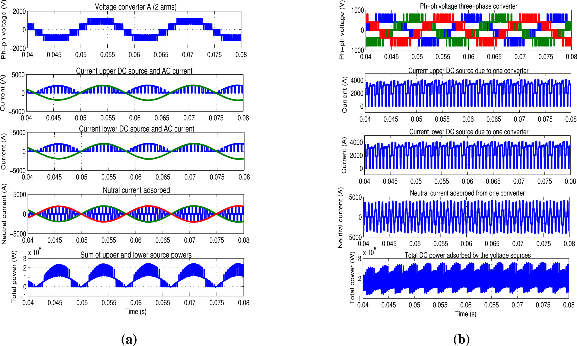
Figure 7a,b, the waveforms relative to the single-phase converters and three-phase converters are represented: the total single-phase converter voltage with five voltage levels (each single-phase arm introduces three levels), the upper and lower DC current (blue) and AC current (green), the neutral current (blue) and the overall DC power are depicted, respectively. It is easy to see that the single-phase DC current has a second harmonic component, and the current derived from the neutral point is null on average. In the three-phase case, the second harmonic disappears, and the first harmonic is the switching frequency.
In
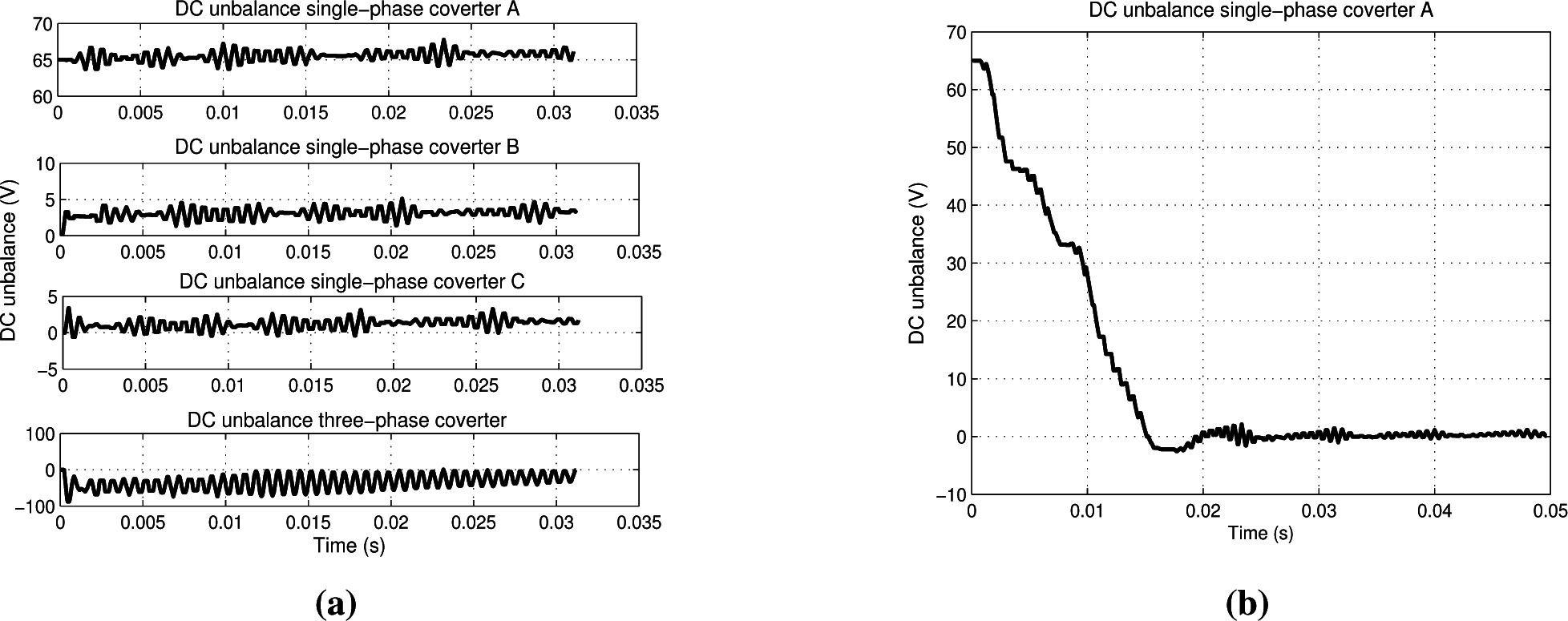
Figure 8, the operation of the single-phase balancing circuit is shown: imposing an initial voltage unbalance on one single-phase source without balancing circuits, the unbalance remains, while with the balancing circuit, the unbalance is removed.
In
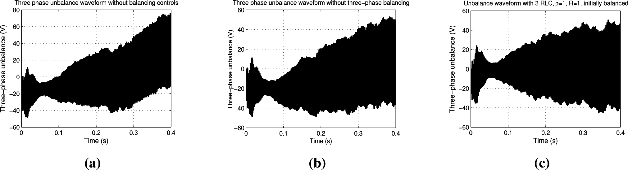
Figure 9, the operation of the three-phase RLC balancing circuit is represented with initially balanced capacitors: without the RLC balancing circuit, the single-phase balancing circuits affect the three-phase unbalance (comparison between
Figure 9a,b), but a better result is obtained with the contribution of the three-phase balancing circuit (
Figure 9c).
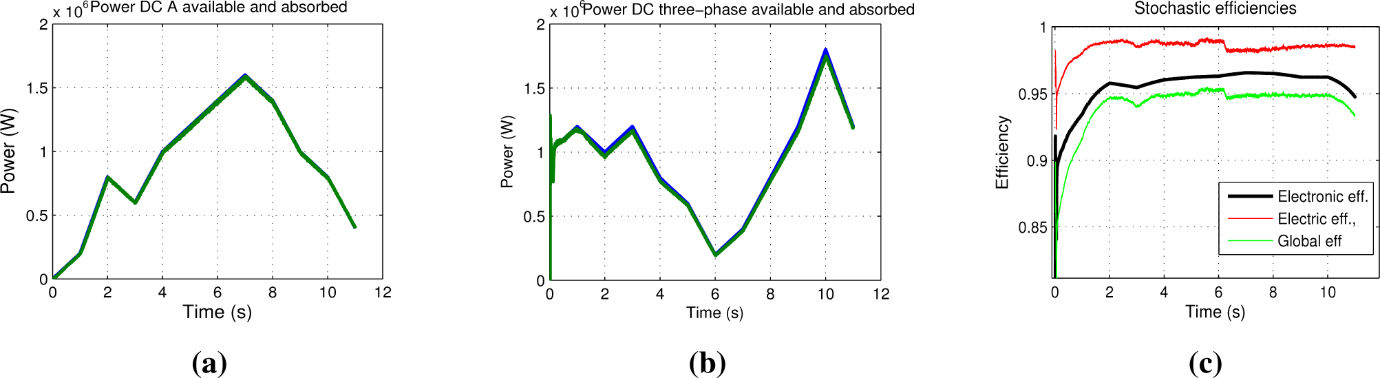
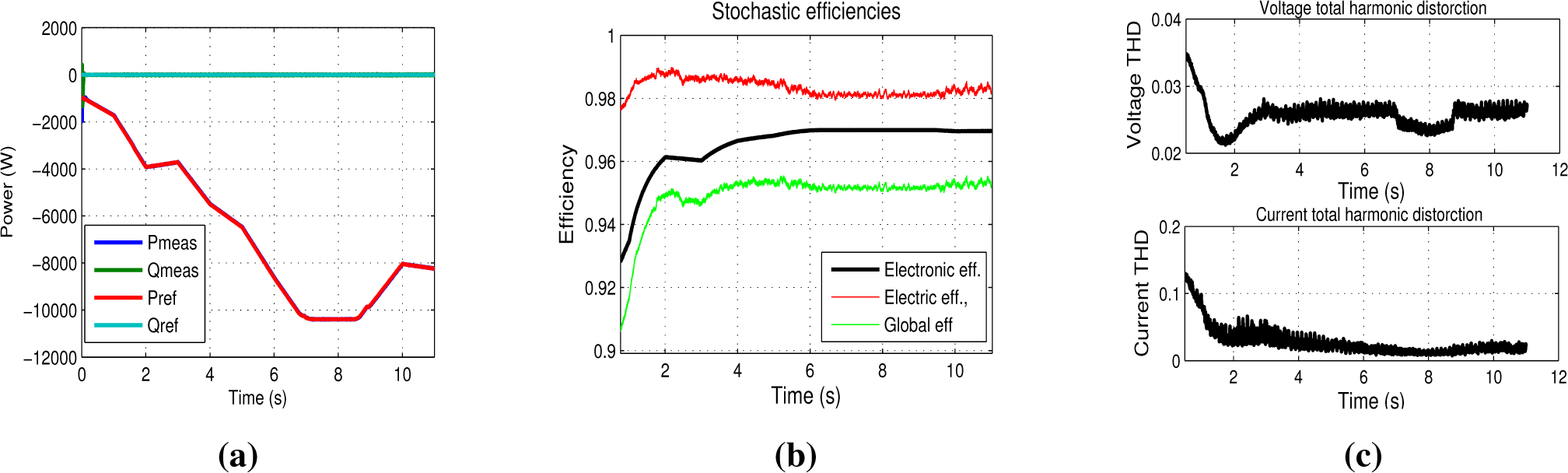
Finally, a stochastic model has been adopted for single and three-phase sources, as shown in
Figure 10a,b. The power associated with the DC buses has been considered to be equal for all single-phase converters. If this hypothesis is removed, the power surplus produced must be cut. The DC power absorbed is lower than the one available because of the power losses; the efficiency is reported in
Figure 10c, where the electronic efficiency considers the power converter losses, the electric efficiency considers the power losses associated with the resistive elements (transformer, ZSBTs, filter), and the global efficiency is the product of the previous terms and the overall efficiency.
The efficiency of the converters has been calculated taking
IGBT as the reference and at the power point
P = 5 MW in this simulation result
η = 96.55%. The global conversion efficiency in this simulation is approximately 95.1%, as shown in
Figure 10c, considering a switching frequency
f = 1, 500 Hz, which is quite high for high power applications: this allows a good reduction of the filtering requirements, since a three-phase inductance
L = 60
µH has been used. The switching frequency may be reduced to increase the efficiency once the converter performances have been tested: if the
THD and the harmonic requirements are in accordance with the standards that regulate the grid-connection, the switching frequency reduction will give a proportional reduction in the switching losses. The filtering inductance may also be increased allowing a further reduction of the switching frequency: the optimal compromise has to be found for each application considering the different constraints on the efficiency and on the filter parameters, such as weight, size and costs. Once these constraints have been defined, the optimal switching frequency and the optimal switch configuration have to be found satisfying the grid-connection standards.
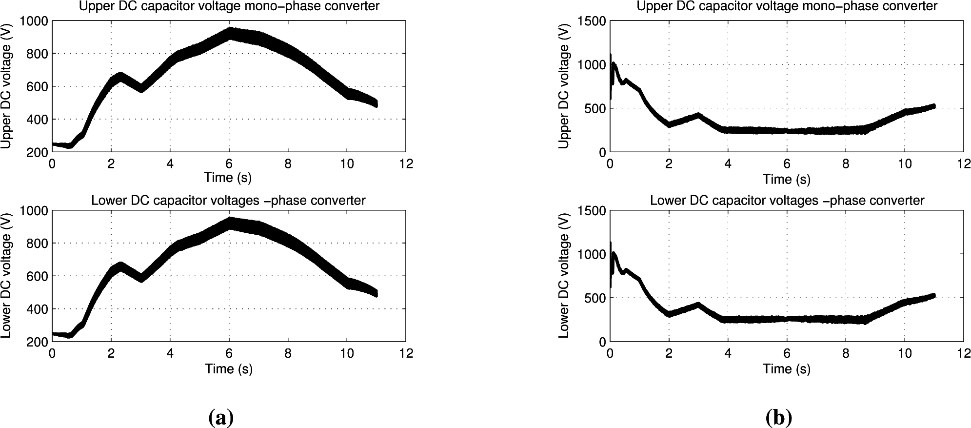
In
Figure 11, the capacitor voltages of the single-phase and three-phase DC links have been depicted: the voltage is variable according to the power available from the source. In
Figure 11b, the three-phase DC voltages have a flat top centered at
V = 250 V; this limit has been implemented in order to avoid the voltage inversion on the electrolytic capacitors, which may destroy the components themselves.
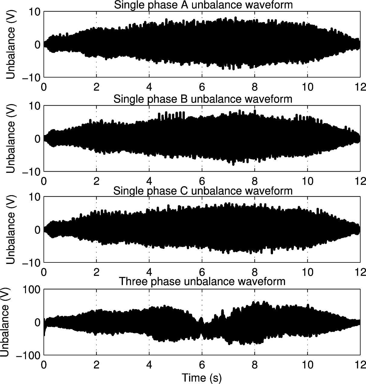
Figure 12 shows the neutral voltage of all of the converters during the stochastic simulation: the voltage has been expressed as the difference between the upper and lower capacitors voltages. The level 0 V represents that the neutral point voltage is exactly half the DC bus voltage. In the three-phase plot, the neutral voltage waveform is not centered at 0 V in the time interval
t = (5–7) s: in fact, the power injected and the voltage applied by the three-phase converter during this time period is low, and also, the current flowing through the RLC circuit will be low, giving a reduced balancing capability.
In
Figure 13, the available power has been increased in order to reach the switches’ current limit; the maximum power with the transformer ratio
k = 0.5 is higher than
P = 10 MW, and the minimum voltage that must be produced on the converter side to reach the grid voltage considering the wye-wye transformer connection is:
Therefore, one three-phase converter is able to provide this voltage remaining in the linear modulation region with low THD if the single-phase converters are not producing and the other three-phase converter is out of service.


