
Heterojunction Diodes and Solar Cells Fabricated by Sputtering of GaAs on Single Crystalline Si

Abstract
:
1. Introduction
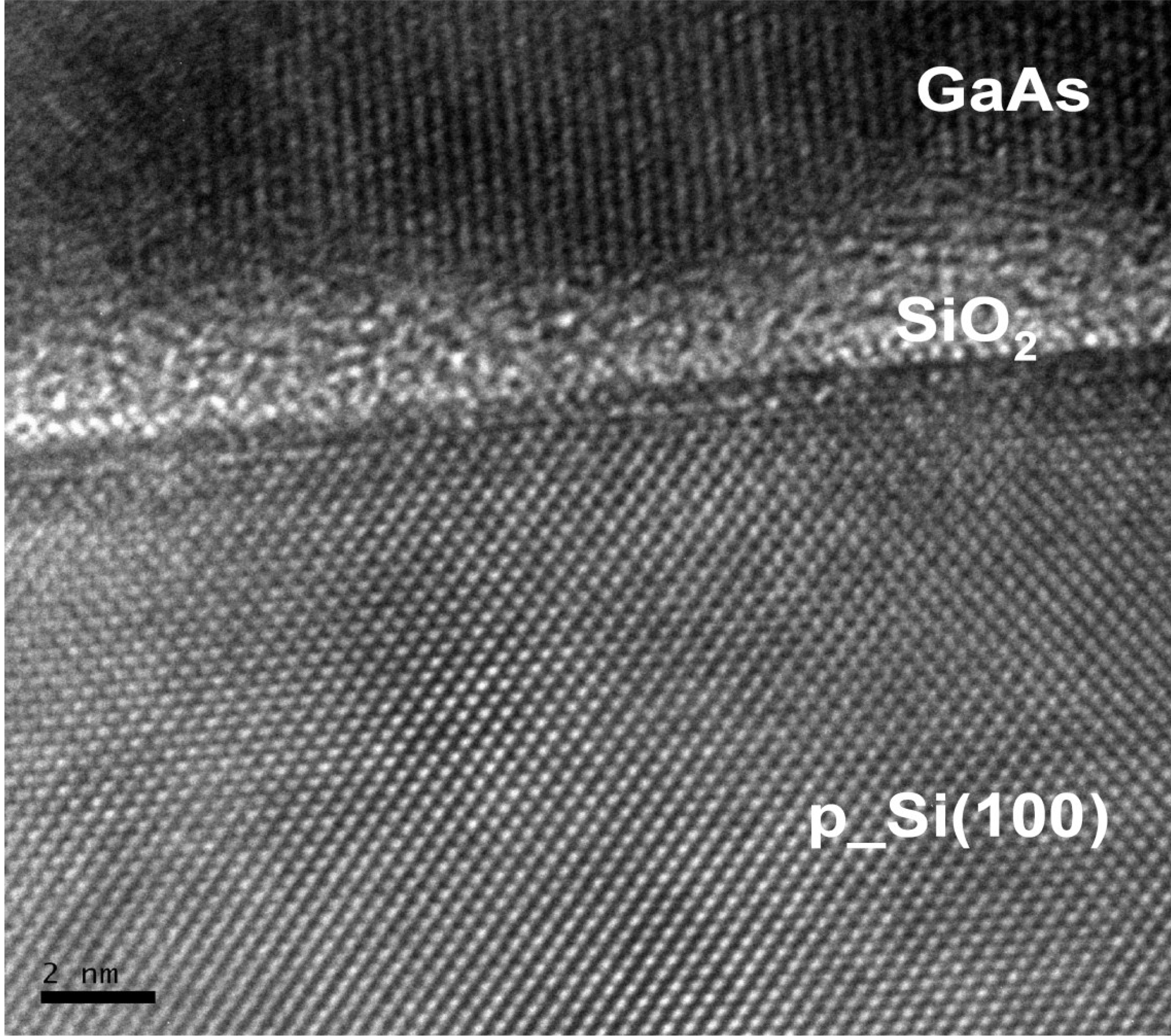
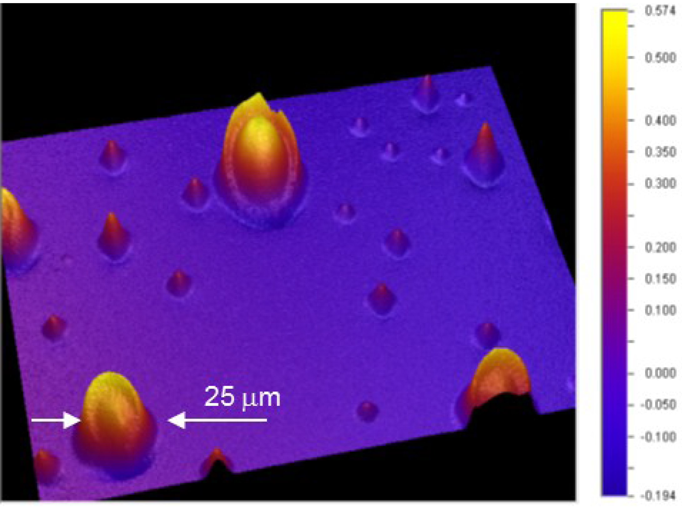
2. Device Preparation
3. Results and Discussion
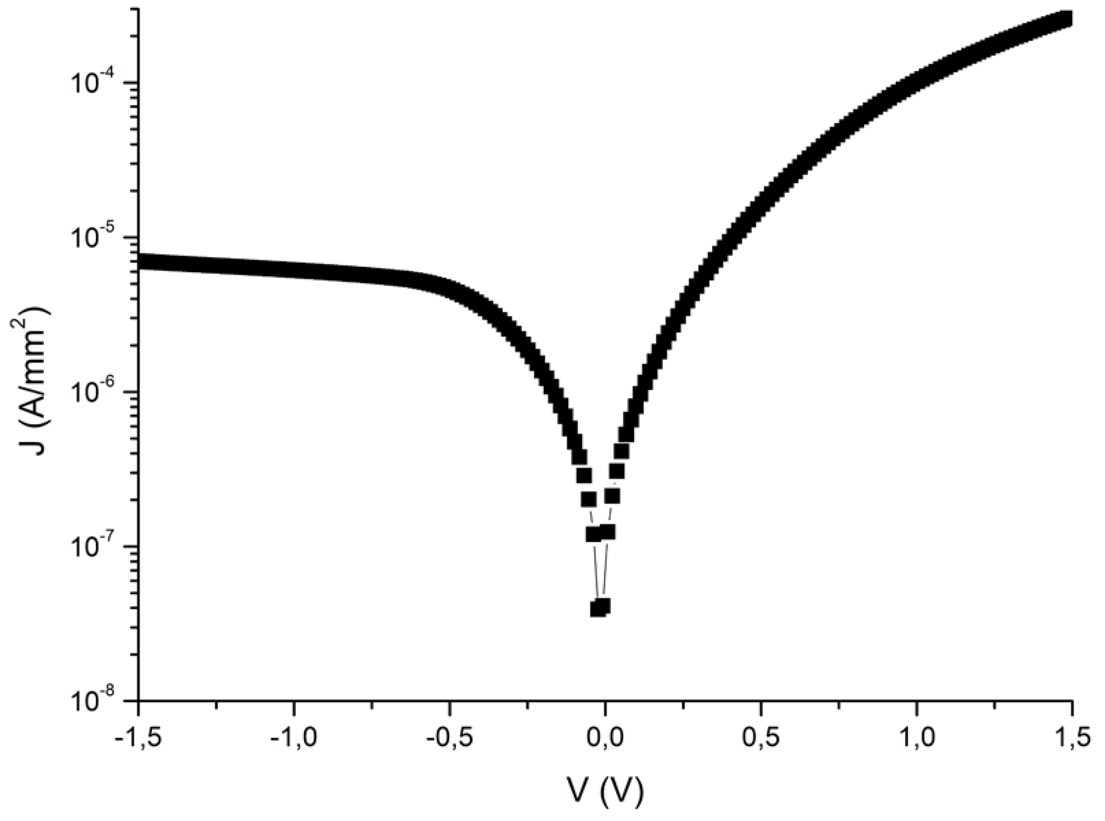
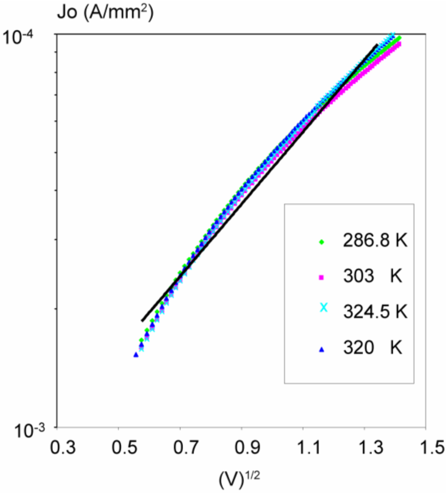
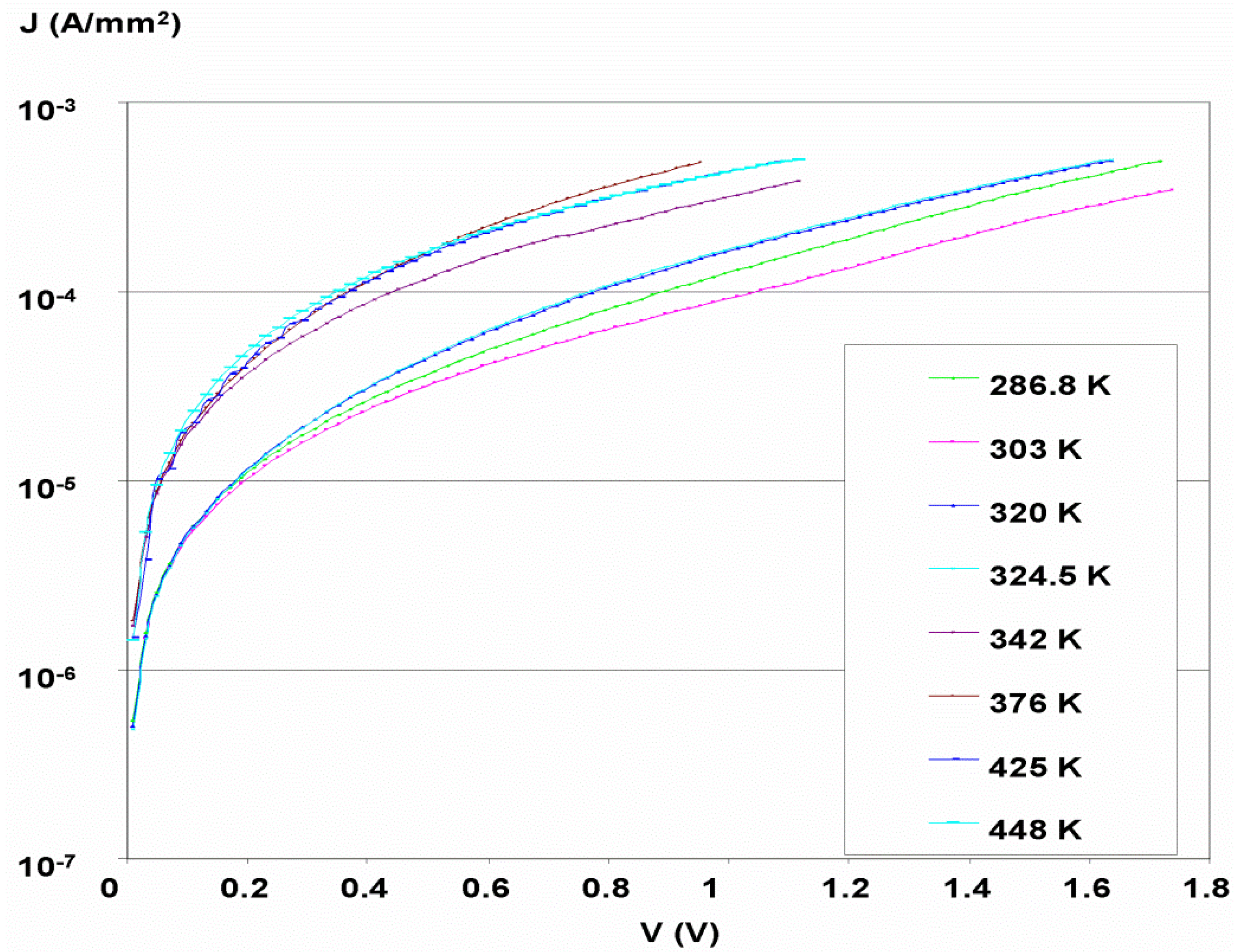
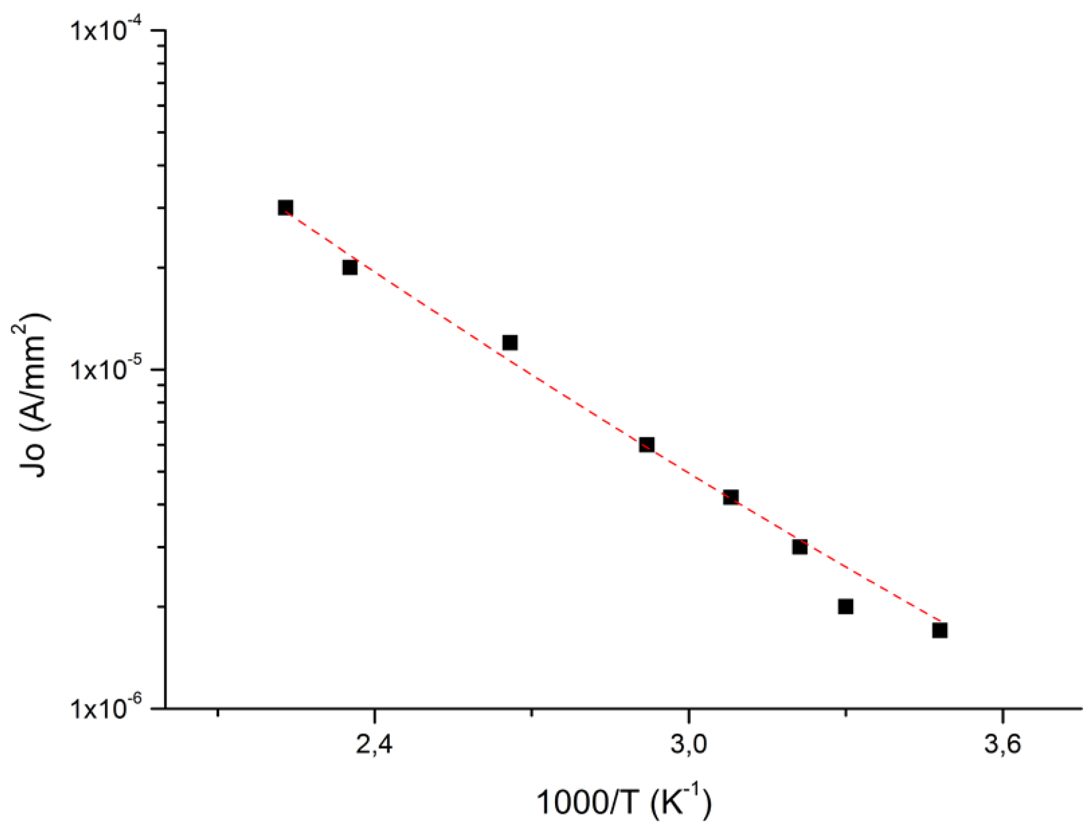
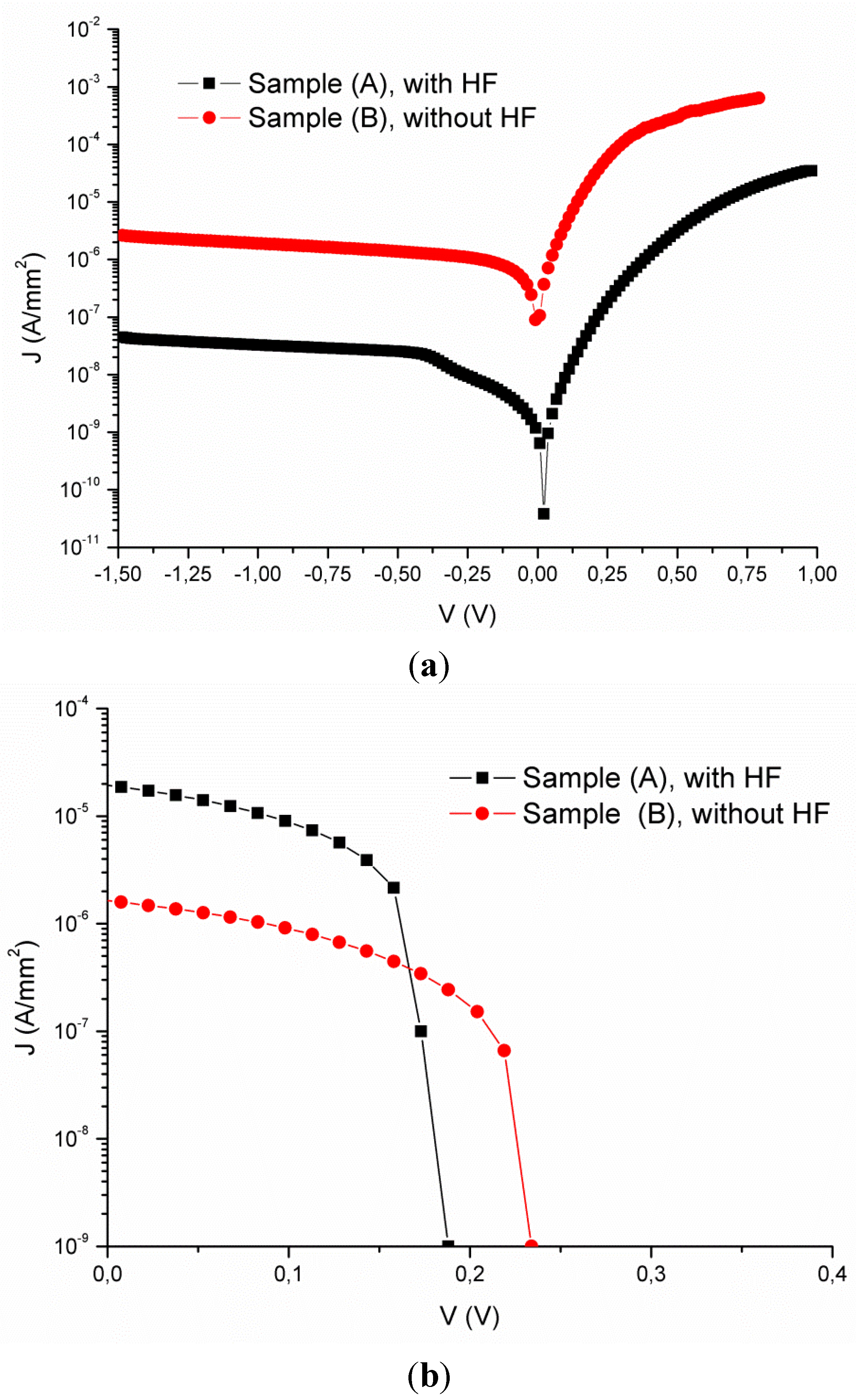
3.1. Diode Current-Voltage Characteristics


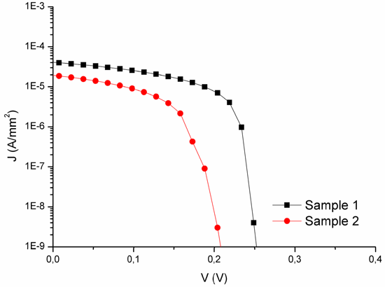
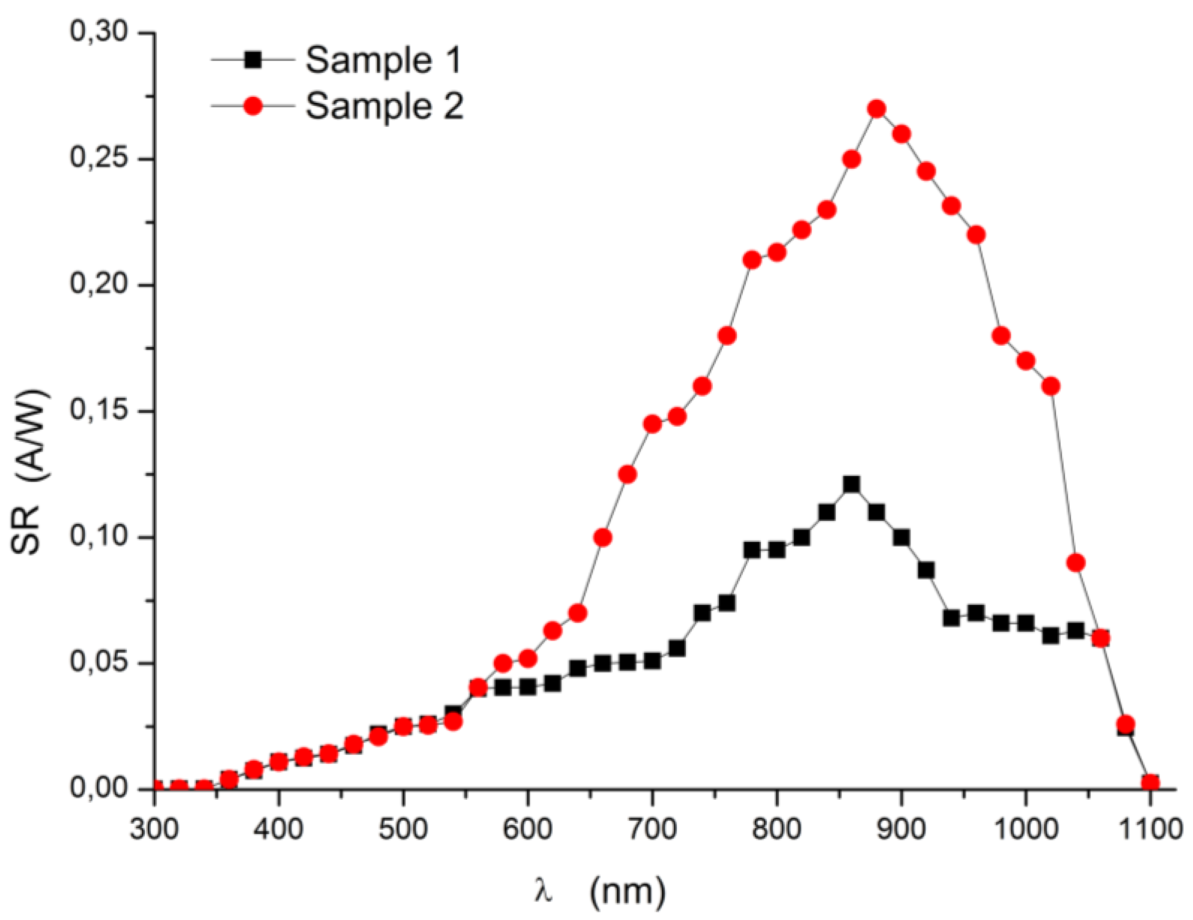
3.2. Solar Cell Photovoltaic Characteristics


| Sample A (with HF) | Sample B (without HF) | |
|---|---|---|
| Rs (Ω) | 1880 | 4390 |
| Rp (Ω) | 112 | 240 |
| FF (%) | 25.6 | 10.36 |


4. Conclusions
Acknowledgments
Author Contributions
Conflicts of Interest
References
- Lopatin, S.; Pennycook, S.J.; Narayan, J.; Duscher, G. Z-contrast imaging of dislocation cores at the GaAs/Si interface. Appl. Phys. Lett. 2002, 81, 2728–2730. [Google Scholar] [CrossRef]
- Georgakilas, A.; Stoemenos, J.; Tsagaraki, K.; Komninou, Ph.; Flevaris, N.; Panayotatos, P.; Christou, A. Generation and annihilation of antiphase domain boundaries in GaAs on Si grown by molecular beam epitaxy. J. Mater. Res. 1993, 8, 1908–1921. [Google Scholar] [CrossRef]
- Georgakilas, A.; Aperathitis, E.; Foukaraki, V.; Kayambaki, M.; Panayotatos, P. Investigation of the GaAs/Si heterojunction band lineup with capacitance and current versus voltage measurements. Mater. Sci. Eng. B 1997, 44, 383–386. [Google Scholar] [CrossRef]
- Aperathitis, E.; Kayiambaki, M.; Foukaraki, V.; Halkias, G.; Panayotatos, P.; Georgakilas, A. Heterojunction diodes nGaAs/pSi with ideal characteristics. Appl. Surf. Sci. 1996, 102, 208–211. [Google Scholar] [CrossRef]
- Trelenberg, T.W.; Dinh, L.N.; Saw, C.K.; Stuart, B.C.; Balooch, M. Femtosecond pulsed laser ablation of GaAs. Appl. Surf. Sci. 2004, 21, 364–369. [Google Scholar] [CrossRef]
- Acharya, K.P.; Khatri, H.; Ullrich, B. Physical characterization of n-GaAs on p-Si formed by low-temperature pulsed-laser deposition. J. Appl. Phys. 2009, 105, 103111.1–103111.5. [Google Scholar] [CrossRef]
- Ullrich, B.; Erlacher, A. Rectification and intrinsic photocurrent of GaAs/Si photodiodes formed with pulsed-laser deposition at 1064 nm. Appl. Phys. Lett. 2005, 87, 151115.1–151115.3. [Google Scholar] [CrossRef]
- Ullrich, B.; Erlacher, A. Photosensitive hetero-pairing of p-GaAs/n-Si by pulsed-laser deposition. J. Phys. D: Appl Phys. 2005, 38, 4048–4051. [Google Scholar] [CrossRef]
- Kawanami, H. Heteroepitaxial technologies of III-V on Si. Sol. Energy Mater. Sol. Cells 2001, 66, 479–486. [Google Scholar]
- Carlin, J.A.; Ringel, S.A.; Fitzgerald, E.A.; Bulsara, M. High Quality GaAs Growth by MBE on Si Using GeSi Buffers and Prospects for Space Photovoltaics. Prog. Photovoltaics 2000, 8, 323–332. [Google Scholar] [CrossRef]
- Usami, N.; Azuma, Y.; Ujihara, T.; Sazaki, G.; Nakajima, K.; Yakabe, Y.; Kondo, T.; Koh, S.; Shiraki, Y.; Zhang, B.; Segawa, Y.; et al. SiGe bulk crystal as a lattice-matched substrate to GaAs for solar cell applications. Appl. Phys. Lett. 2000, 77, 3565–3567. [Google Scholar] [CrossRef]
- Ringel, S.A.; Carlin, J.A.; Andre, C.L.; Hudait, M.K.; Gonzalez, M.; Wilt, D.M.; Clark, E.B.; Jenkins, P.; Scheiman, D.; Allerman, A.; et al. Single-junction InGaP/GaAs Solar Cells Grown on Si Substrates with SiGe Buffer Layers. Prog. Photovolt. 2002, 10, 417–426. [Google Scholar] [CrossRef]
- Ringel, S.A.; Andre, C.L.; Fitzgerald, E.A.; Pitera, A.J.; Wilt, D.M. Multijunction III-V photovoltaics on lattice-engineered Si substrates. In Proceedings of the Conference Record of the Thirty-First IEEE Photovoltaic Specialists Conference, Piscataway, NJ, USA, 3–7 January 2005; pp. 567–570.
- Itoh, Y.; Nishioka, T.; Yamamoto, A.; Yamaguchi, M. 14.5% conversion efficiency GaAs solar cell fabricated on Si substrates. Appl. Phys. Lett. 1986, 49, 1614–1616. [Google Scholar] [CrossRef]
- Yamaguchi, M.; Ohmachi, Y.; Oh’hara, T.; Kadota, Y.; Imaizumi, M.; Matsuda, S. GaAs solar cells grown on Si substrates for space use. Prog. Photovolt. 2001, 9, 191–201. [Google Scholar] [CrossRef]
- Wang, G.; Ogawa, T.; Soga, T.; Egawa, T.; Jimbo, T.; Umeno, M. Hydrogenation of GaAs-on-Si Schottky diodes by PH3 -added H2 plasma. Appl. Surf. Sci. 2000, 159–160, 191–196. [Google Scholar] [CrossRef]
- Wang, G.; Ogawa, T.; Umeno, M.; Soga, T.; Jimbo, T. Surface and bulk passivation of GaAs solar cell on Si substrate by H2+PH3 plasma. Appl. Phys. Lett. 2000, 76, 730–732. [Google Scholar] [CrossRef]
- Shimizu, Y.; Okada, Y. Growth of high-quality GaAs/Si films for use in solar cell applications. J. Crystal Growth 2004, 265, 99–106. [Google Scholar] [CrossRef]
- Carioul, R.; Maurice, J.L.; Decobert, J.; Cabarrocas, P.R.I. Direct Epitaxial Growth of Silicon on GaAs by Low Temperature Epitaxy. In Proceedings of the 40th IEEE Photovoltaic Specialist Conference (PVSC), Denver, CO, USA, 8–13 June 2014; pp. 2789–2791.
- Fennouh, A.; Aguir, K.; Carchano, H.; Seguin, J.L. Electrical characteristics of amorphous GaAs-n-crystalline Si heterojunctions. Mater. Sci. Eng. B 1995, 34, 27–31. [Google Scholar] [CrossRef]
- Aguir, K.; Fennouh, A.; Carchano, H.; Seguin, J.L.; Elhadadi, B.; Lalande, F. Electrical properties of a-GaAs/c-Si(p) heterojunctions. Thin Solid Films 1995, 257, 98–103. [Google Scholar] [CrossRef]
- Galiana, B.; Silvestre, S.; Algora, C.; Rey-Stolle, I. Effect of annealing atmosphere in the properties of GaAs layers deposited by sputtering techniques on Si substrates. J. Mater. Sci.: Mater. Electron. 2014, 25, 134–139. [Google Scholar] [CrossRef]
- Silvestre, S.; Boronat, A.; Colina, M.; Castañer, L.; Olea, J.; Pastor, D.; Del Prado, A.; Mártil, I.; González-Díaz, G.; Luque, A.; et al. Sub-Bandgap external quantum efficiency in Ti implanted Si heterojunction with intrinsic thin layer cells. Jpn. J. Appl. Phys. 2013, 52, 122302:1–122302:5. [Google Scholar] [CrossRef]
- Kang, H.J.; Moon, Y.M.; Kang, T.W.; Leem, J.Y.; Lee, J.J.; Ma, D.S. Surface composition and structure changes in GaAs compounds due to low‐energy Ar+ ion bombardment. J. Vac. Sci. Technol. A 1989, 7, 3251–3255. [Google Scholar] [CrossRef]
- Boronat, A.; Silvestre, S.; Fuertes Marron, D.; Castañer, L.; Martı, A.; Luque, A. Optical absorption of radio frequency sputtered GaAs(Ti) films. J. Mater. Sci. Mater. Electron. 2013, 24, 993–998. [Google Scholar] [CrossRef]
- Campomanes, R.R.; Dias da Silva, J.H.; Vilcarromero, J.; Cardoso, L.P. Crystallization of amorphous GaAs films prepared onto different substrates. J. Non-Cryst. Solids 2002, 299–302, 788–792. [Google Scholar] [CrossRef]
- Campomanes, R.R.; Vilcarromero, J.; Galzerani, J.C.; Dias da Silva, J.H. The evolution of arsenic excess induced by thermal annealing in arsenic-rich Ga1-xAsx films. Appl. Phys. A 2005, 80, 267–269. [Google Scholar] [CrossRef]
- Silvestre, S.; Puigdollers, J.; Boronat, A.; Castañer, L. Analysis of GaAs-Ti thin films deposited by sputtering onto c-Si and GaAs. In Proceedings of the 7th Spanish Conference on Electron Devices, Santiago de Compostela, Spain, 11–13 February 2009; García, A., Seoane, N., Aldegunde, M.A., Figueroa, C., Eds.; pp. 250–252.
- Riben, A.R.; Feucht, D.L. nGe-pGaAs Heterojunctions. Solid State Electron. 1966, 9. [Google Scholar] [CrossRef]
- Matsuura, H.; Okuno, T.; Okushi, H.; Tanaka, K. Electrical properties of n‐amorphous/p‐crystalline silicon heterojunctions. J. Appl. Phys. 1984, 55. [Google Scholar] [CrossRef]
- Kaniewska, M.; Klima, K. Investigations of surface defects of GaAs grown by molecular beam epitaxy. Mat. Sci. Eng. B 2002, 91–92, 512–515. [Google Scholar] [CrossRef]
- Klima, K.; Kaniewska, M.; Reginski, K.; Kaniewski, J. Oval Defects in the MBE Grown AlGaAs/InGaAs/GaAs and InGaAs/GaAs Structures. Cryst. Res. Technol. 1999, 34, 683–687. [Google Scholar]
- Gibson, E.M.; Foxon, C.T.; Zhang, J.; Joyce, B.A. Gallium desorption from GaAs and (Al,Ga)As during molecular beam epitaxy growth at high temperatures. Appl. Phys. Lett. 1990, 57. [Google Scholar] [CrossRef]
© 2015 by the authors; licensee MDPI, Basel, Switzerland. This article is an open access article distributed under the terms and conditions of the Creative Commons Attribution license (http://creativecommons.org/licenses/by/4.0/).
Share and Cite
Silvestre, S.; Boronat, A. Heterojunction Diodes and Solar Cells Fabricated by Sputtering of GaAs on Single Crystalline Si. Electronics 2015, 4, 261-273. https://doi.org/10.3390/electronics4020261
Silvestre S, Boronat A. Heterojunction Diodes and Solar Cells Fabricated by Sputtering of GaAs on Single Crystalline Si. Electronics. 2015; 4(2):261-273. https://doi.org/10.3390/electronics4020261
Chicago/Turabian StyleSilvestre, Santiago, and Alfredo Boronat. 2015. "Heterojunction Diodes and Solar Cells Fabricated by Sputtering of GaAs on Single Crystalline Si" Electronics 4, no. 2: 261-273. https://doi.org/10.3390/electronics4020261
APA StyleSilvestre, S., & Boronat, A. (2015). Heterojunction Diodes and Solar Cells Fabricated by Sputtering of GaAs on Single Crystalline Si. Electronics, 4(2), 261-273. https://doi.org/10.3390/electronics4020261