Article

Electromagnetic-Thermal Coupling Modeling and Analysis of High-Speed Transmission Line on LTCC Substrate in SiP


Center for Target Cognition Information Processing Science and Technology, College of Information and Communication Engineering, Beijing Information Science and Technology University, Beijing 102206, China
*
Author to whom correspondence should be addressed.
Electronics 2026, 15(8), 1668; https://doi.org/10.3390/electronics15081668
Submission received: 18 March 2026 / Revised: 12 April 2026 / Accepted: 13 April 2026 / Published: 16 April 2026

Abstract

With the growing simultaneous demands for miniaturization and high performance, thermal issues such as hotspots severely degrade the high-speed signal transmission performance of low temperature co-fired ceramic (LTCC) substrate in system-in-package (SiP) modules. This paper proposes a high-speed transmission line design for LTCC substrates, using a G-S (Ground-Signal) structure to ensure reliable signal transmission quality. Based on this structure, finite element simulations are performed to investigate the electromagnetic signal transmission characteristics under both uniform and non-uniform thermal fields, confirming that signal transmission efficiency exhibits strong temperature dependence. The results indicate that when the temperature exceeds 50 °C, non-uniform temperature distributions exert a significantly stronger influence on electromagnetic performance, leading to aggravated signal reflections and reduced transmission efficiency. At 300 °C, the transmission efficiency under non-uniform temperature drops to 35.0%, which is a 61.8% decrease compared with the optimal scheme obtained under ideal electric field conditions. Under electromagnetic-thermal coupling, a comparative study of different schemes shows that the optimal design derived from a single electric field is not suitable for electromagnetic-thermal coupled working conditions. The optimized Scheme 2 increases transmission efficiency to about 75.3%, with smoother S-parameter curves and smaller fluctuations. These findings provide valuable references for subsequent reliability-oriented design and experimental verification.

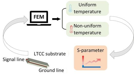
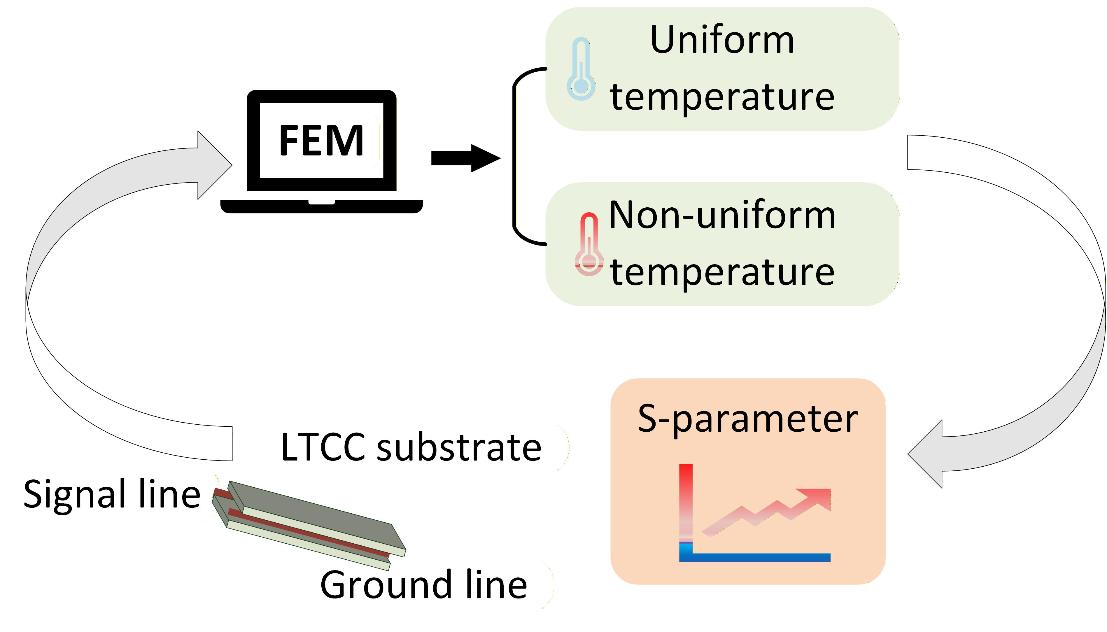
Graphical Abstract

1. Introduction

With the continuous development of electronic technology, modern electronic products feature high integration, multifunctionality, and high-power consumption [1,2]. This imposes strict requirements on high-quality signal transmission, good hermeticity, small size, light weight, excellent electrical performance, and effective thermal management [3,4]. However, the continuously shrinking feature sizes of electronic devices make them vulnerable to thermal crosstalk, especially for LTCC substrates in SiP under high-temperature operating conditions [5,6]. Notably, under actual operating conditions, the system is exposed not only to uniform thermal environments but also to steep temperature gradients at local hotspots, which further accelerate performance degradation. Electromagnetic-thermal coupling [7,8,9] has a considerable impact on the electromagnetic transmission efficiency of signals [10,11,12]. However, related research is still insufficient, requiring an in-depth study of electromagnetic signal transmission performance under thermal environments.
Signal transmission performance is crucial to the overall functional reliability of the system [13,14,15]. Ge et al. [16] applied a novel wire-bonding interconnection compensation structure to highly integrated microwave hybrid integrated circuits. By using a multilayer packaging system to strengthen heat dissipation, they increased the bandwidth and improved signal transmission performance. Lu et al. [17] proposed an electro-thermal co-simulation method based on the finite element method for analyzing high-power RF/microwave circuits. By accounting for thermal effects simultaneously, this method reduces the sensitivity of electronic equipment to temperature variations and provides an accurate and efficient method to analyze the electrical characteristics of such devices. Yang et al. [18] verified a 2.5D microsystem packaging simulation model, taking a specific 2.5D structure as the research object. By combining the multiphysics co-optimization design of TSV interposer structures with the Hammerstein experimental design method and genetic algorithms, they achieved an 80% improvement in the electrical signal transmission efficiency of the TSV interposer. However, most existing studies focus on the effects of electric fields or uniform thermal fields on transmission performance, whilst research on the influence of non-uniform thermal fields on signal transmission is still relatively limited. Compared with existing studies, the core innovations of this work are twofold. First, at the modeling level, we break through the traditional idealized uniform temperature field assumption and establish a multiphysics electromagnetic-thermal coupling model that accounts for local hotspots, which can more realistically reflect the actual working conditions of the device. Second, at the methodological level, by comparing electromagnetic responses under uniform and non-uniform temperature fields, we quantitatively reveal the mechanism by which temperature gradients and local hotspots affect the electromagnetic performance of LTCC substrates in SiP modules.
This work presents a numerical study based on finite element analysis in COMSOL 6.2 Multiphysics, focusing on the electromagnetic-thermal coupling behavior of the proposed structure. A G-S type high-speed transmission line for LTCC substrates in SiP is designed and numerically characterized. To evaluate the thermal reliability of the transmission line, both uniform and non-uniform temperature field conditions are set up, and the influence of thermal effects on the transmission performance of the LTCC-based transmission line in the SiP system is systematically studied [19,20,21]. Under an ideal electric field, signal transmission efficiency is enhanced by optimizing key structural parameters such as the width, spacing, and thickness of the transmission line. Then, under electromagnetic-thermal coupling conditions, the effects of uniform and non-uniform thermal fields on signal scattering characteristics are compared and analyzed. Finally, based on the comparisons among different design schemes, it is concluded that the preferred design obtained from a single physical field is no longer applicable under multi-field coupling conditions [22,23,24]. This work is expected to provide a theoretical foundation for subsequent reliability evaluation and experimental research.

2. Simulation Experiment

2.1. Finite Element Model

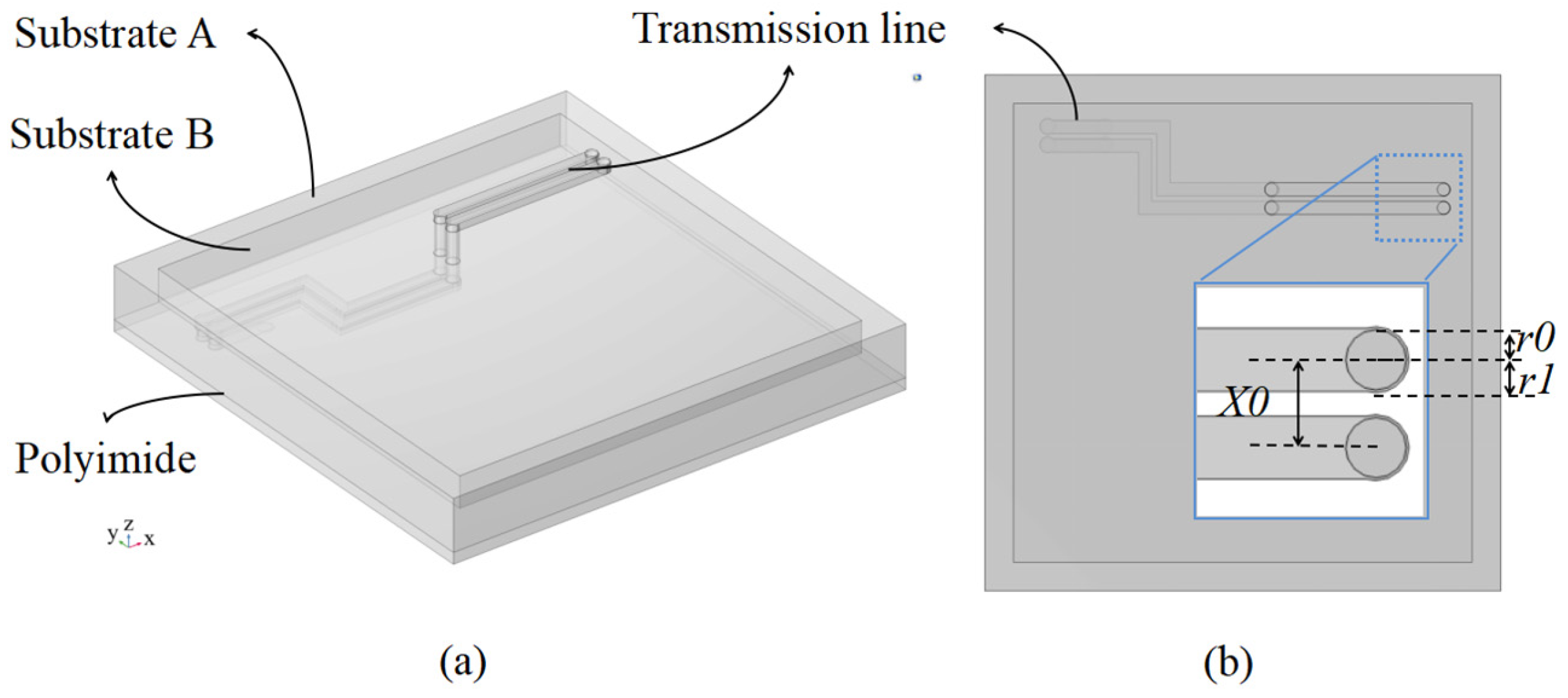
On the LTCC substrate, a high-speed transmission line combining microstrip and stripline structures is designed to form a G-S (Ground-Signal) configuration. This layout represents a typical signal transmission configuration widely used in SiP structures based on LTCC substrates. With an operating frequency range of 1–30 GHz, it features low loss and high integration, satisfying the requirements of high-power RF systems and microwave components for aerospace applications. The specific parameters of this design are presented in Figure 1a,b. The detailed structural dimensions are listed in Table 1, where the transmission line length (L), width (W), spacing (S), height (H), through-ceramic via (TCV), and pad radius (R) are represented by L, w0, X0, d1, r0 and r1, respectively.

2.2. Boundary Condition

This paper adopts an electromagnetic-thermal coupled finite element method to carry out multiphysics simulation analysis. The electromagnetic simulation uses the frequency-domain electric field wave equation to describe the electromagnetic field distribution, which is expressed as:
× μ r 1 ( × E ) κ 0 2 ( ε r j σ ω ε 0 ) E = 0
κ 0 = ω μ 0 ε 0
In these equations, E is the electric field intensity vector, μr and εr are the relative magnetic permeability and relative permittivity of the material, respectively, σ is the electrical conductivity, ω is the angular frequency, ε0 is the vacuum permittivity, and k0 is the free-space wave number.
The thermal simulation employs transient energy conservation equations that include convection terms and thermoelastic damping, which are expressed as:
ρ C p u T + q = Q + Q ted
q = k T
In these equations, ρ, Cp and k denote the density, specific heat at constant pressure, and thermal conductivity of the material, respectively; T is the temperature field; ∇T is the temperature gradient; Q is the volumetric heat source from electromagnetic losses; Qted is the thermoelastic damping heat source; q is the heat flux density vector; and u is the fluid velocity vector, which is set to 0 in the solid domain.
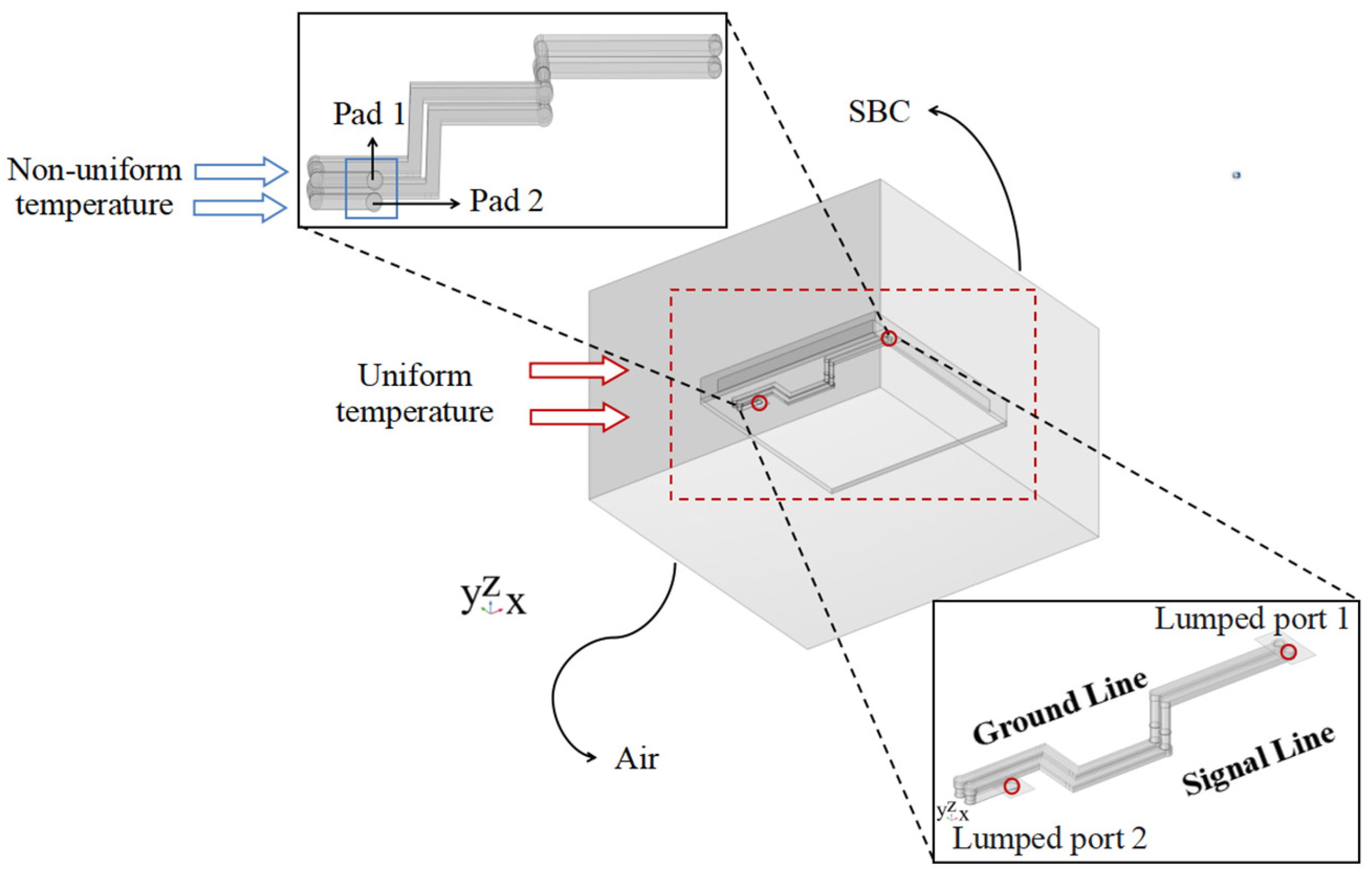
The model is solved using the “Electromagnetic Waves” interface. Scattering boundary conditions (SBC) are applied to simulate an open-space environment. All metals exhibit losses during signal transmission; therefore, transition boundary conditions are adopted in this model. The two transmission lines correspond to the signal line and the ground line, respectively. Excitation and load termination are applied via coaxial lumped port 1 and lumped port 2, both set to a reference impedance of 50 Ω to match the transmission line system. Wave excitation is enabled for lumped port 1 with an input voltage of 1 V, whereas lumped port 2, acting as the load termination, has wave excitation disabled to realize port matching and signal termination only, as shown in Figure 2. Relevant material parameters are detailed in Table 2.
The two pads at the bottom of the structure are fixed to constrain translational and rotational degrees of freedom. For the uniform temperature condition, a uniform temperature load T0 is applied to the entire solid computational domain. For the non-uniform temperature condition, to characterize the local hotspot effect, a spatially distributed temperature field is defined through the solid heat transfer interface. In this case, the bottom pads remain fixed, and a local high temperature T0 is applied only to the pad regions. All other exposed boundaries exchange heat with the ambient environment via convective heat flux, with a convective heat transfer coefficient of 5 W/(m2·K) and the ambient temperature set to room temperature. The complete boundary conditions for both uniform and non-uniform temperature fields are shown in Figure 2.
LTCC-based SiP devices are widely used in extreme environments such as aerospace, automotive electronics, and high-power RF systems. According to relevant reliability standards such as JEDEC JESD402-1B, the temperature load T0 is set to range from −50 °C to 300 °C with a step of 50 °C. This temperature range fully covers the typical harsh service conditions of such devices. It also has strong engineering practicality and can provide a useful reference for the thermo-structural reliability design of related LTCC substrates in SiP components.

3. Analysis and Discussion

3.1. Parameter Enhancement for Electromagnetic Transmission Model

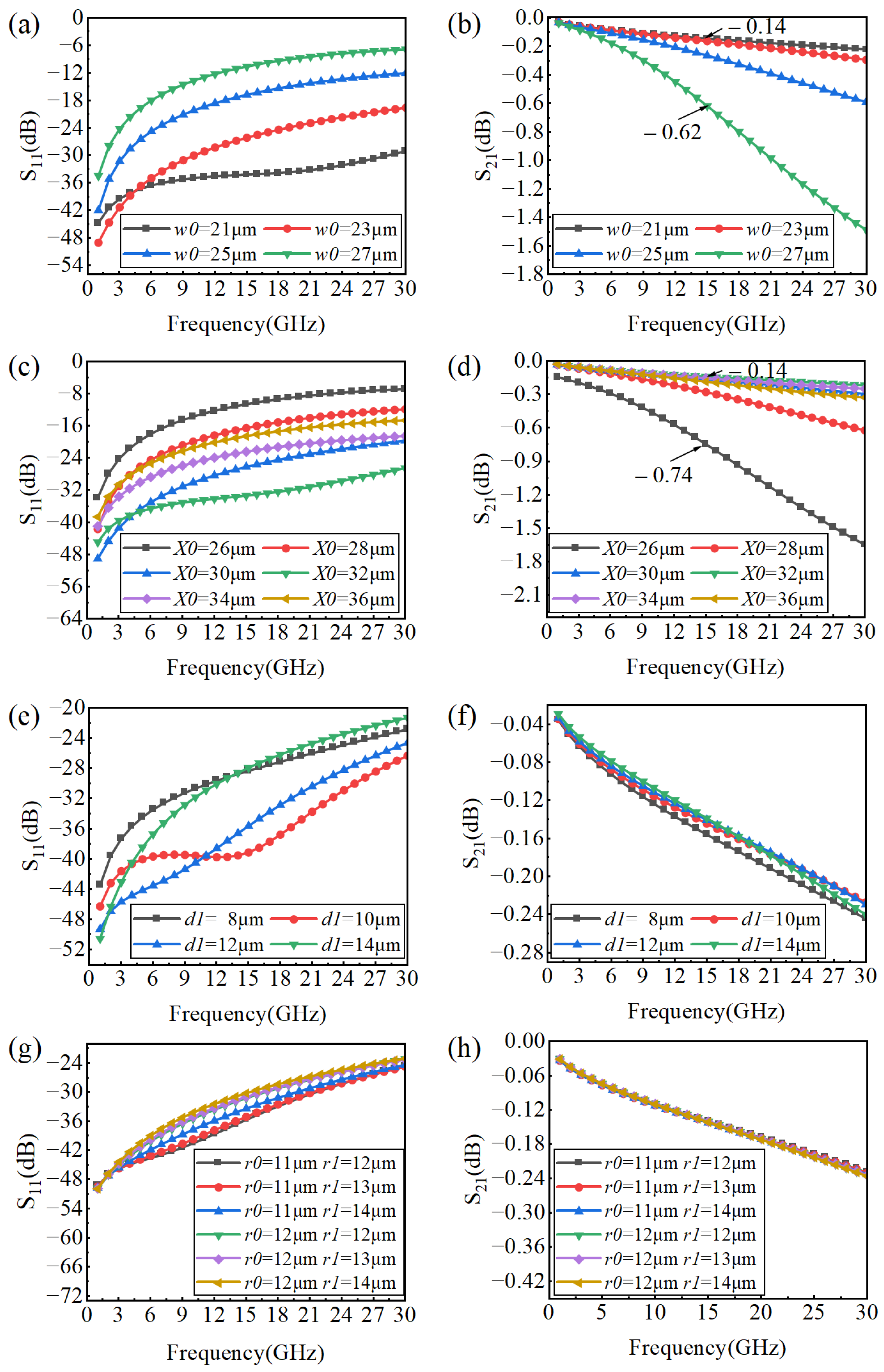
To improve the signal transmission performance of LTCC substrates in SiP under an ideal electric field, key structural parameters including the transmission line width (w0), line spacing (X0), height (d1), TCV radius (r0), and pad radius (r1) are comprehensively adjusted and optimized. Parametric scanning and comparative analysis are performed, and the corresponding electromagnetic response characteristics are summarized in Figure 3. The detailed analysis results are given below:
As shown in Figure 3a,b, the return loss (S11) increases monotonically with the increase in transmission line width (w0), indicating aggravated signal reflection and impedance mismatch. In contrast, the insertion loss (S21) transmission efficiency is improved as the transmission line width (w0) decreases. Specifically, when w0 is set to 21 μm, the energy transmission ratio at the center frequency reaches 96.8%, which is 10.1% higher than that of the reference scheme with a line width of 27 μm (86.7%).
The spacing between adjacent transmission lines also plays a critical role in determining the scattering parameters, as shown in Figure 3c,d. Specifically, when the transmission line spacing (X0) is 32 μm, the energy transmission ratio at the center frequency reaches 96.8%. Compared with the case of 26 μm spacing, the transmission efficiency increases by 12.5%. In practical packaging design, reasonably arranged line spacing is essential: excessively narrow spacing easily introduces crosstalk interference, while overly large spacing reduces layout compactness and degrades high-speed transmission capability.
According to the simulated curves in Figure 3e–h, changes in transmission line height have a negligible effect on electromagnetic scattering characteristics, and the electromagnetic characteristic curves remain stable within the studied range. The recommended optimal height range is determined to be 10 μm to 12 μm. In addition, both TCV radius and pad radius show low sensitivity to high-speed signal transmission performance.
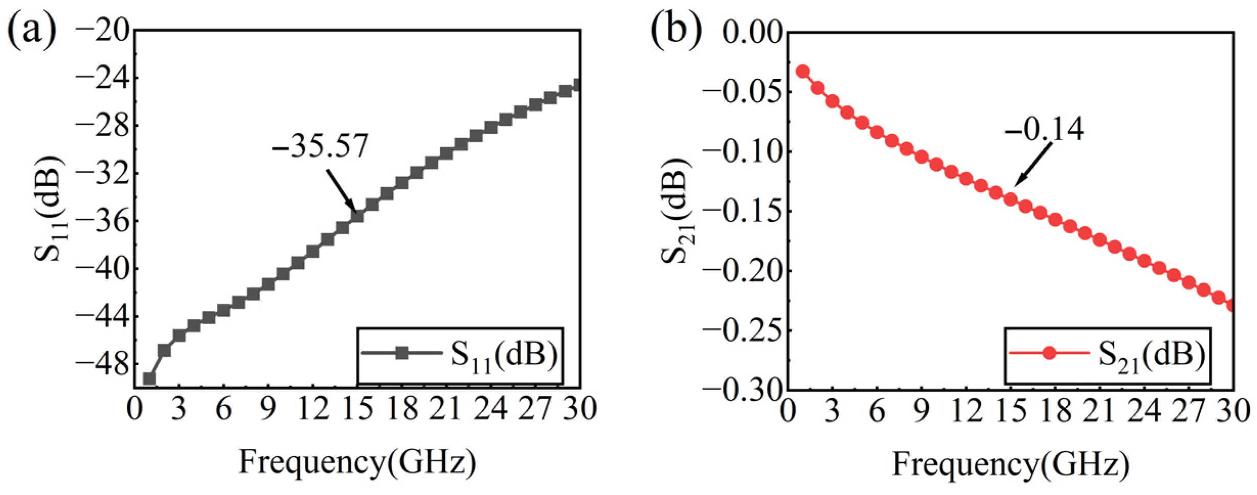
Based on the above analysis, Scheme 1 is chosen as the baseline design with the following parameters: transmission line width (w0) of 23 μm, spacing (X0) of 32 μm, height (d1) of 12 μm, TCV radius (r0) of 11 μm, and pad radius (r1) of 12 μm. With this configuration, the energy transmission ratio at the center frequency reaches 96.8%, and the return loss is significantly lower than −20 dB, as shown in Figure 4a,b.

3.2. Electro-Thermal Coupling Mechanism

Under complex operating conditions, microsystems are subjected to the coupled effects of multiple physical fields. For example, resistive heating caused by current flow generates thermal energy, which in turn changes the temperature distribution of material. This heat diffusion process, governed by the heat conduction equation, is given by Equation (5):
−∇∙(kT) = Q
In this equation, k is the thermal conductivity, T is the temperature, and Q is the volumetric heat source. The temperature field also exerts a reciprocal effect on the electric field distribution, mainly through the Seebeck effect. In numerical simulations, the Joule heating term Q (the source term in Equation (5)) is derived from the electric field and current density, as defined in Equation (6):
Q = JE = σ|∇V|2
Here, J is the current density vector, E is the electric field strength, σ is the electrical conductivity, and ∇V is the electric potential gradient. Since σ is temperature-dependent (σ(T)), the electrostatic field equation is reformulated as Equation (7):
−∇∙(σV) = 0
Additionally, temperature changes induce thermal expansion in the material, which is characterized by thermal strain ε, defined by Equation (8):
ε = α(TTref)
In this expression, α is the thermal expansion coefficient, Tref is the reference temperature, and ε is the thermal strain.
When a transmission line transmits radio-frequency signals, temperature exerts a comprehensive influence on the S-parameters through a multiphysics coupling mechanism involving electrical, thermal and structural factors.
First, the radio-frequency signal current generates an internal heat source through the Joule heating effect. This heat input forms a non-uniform temperature field inside the device, as governed by the heat conduction equation. Temperature changes modify the electrical conductivity of the conductor, directly increasing ohmic losses and disturbing the electric field distribution under the constraint of current conservation. Consequently, this leads to a significant degradation in the insertion loss and return loss of the transmission line.
Meanwhile, temperature causes geometric deformation of the device through the thermal expansion equation. This deformation changes the characteristic impedance and phase constant of the transmission line, leading to phase shifts in the S-parameters and resonance frequency draft of resonant components. In addition, the non-uniform temperature field introduces additional thermoelectric potential perturbations through the Seebeck effect. When superimposed on temperature-dependent changes in dielectric constant and loss tangent, this effect further aggravates transmission losses and impedance mismatch.
Ultimately, the coupled interaction of these electrical, thermal, and structural multi-field effects collectively determines the temperature sensitivity of the S-parameters.
To study the influence of electromagnetic-thermal coupling on LTCC substrate in SiP, comparative numerical simulations are designed under different temperature conditions. In one group of simulations, a uniform temperature field is applied to the system through thermal expansion nodes, while in the other group, the system is subjected to a non-uniform temperature distribution with local hotspots. This approach allows a focused comparison of the effects of these two temperature conditions on the electromagnetic transmission performance of the system.

3.3. The Effect of Thermal Field on Scattering Characteristics

Temperature regulates the electromagnetic properties of materials by changing key constitutive parameters, driven by microscopic thermal motion. A temperature rise increases the amplitude of lattice vibration and the probability of carrier scattering. This directly changes the electrical conductivity and loss characteristics of the material. In metallic conductors, resistivity increases almost linearly with temperature, leading to a rapid increase in conductor losses. In dielectric materials, thermal excitation increases the concentration of weakly bound carriers. This causes both dielectric conductivity and loss tangent to increase simultaneously.
Thermal disturbances also alter the microscopic dynamics of polarization and magnetization. Under electric field excitation, the intensities of electron, ion, and orientation polarization change nonlinearly with temperature. This leads to complex temperature-dependent behavior of relative permittivity. In magnetic materials, thermal energy disrupts the ordered arrangement of magnetic domains. This results in an overall decrease in the relative permeability of ferromagnetic materials with increasing temperature, with a sharp drop near the Curie temperature. These combined changes in constitutive parameters modify the electromagnetic wave impedance and propagation constants in the medium. Ultimately, they cause a shift in the device’s resonant frequency, increased insertion loss, and degraded impedance matching.
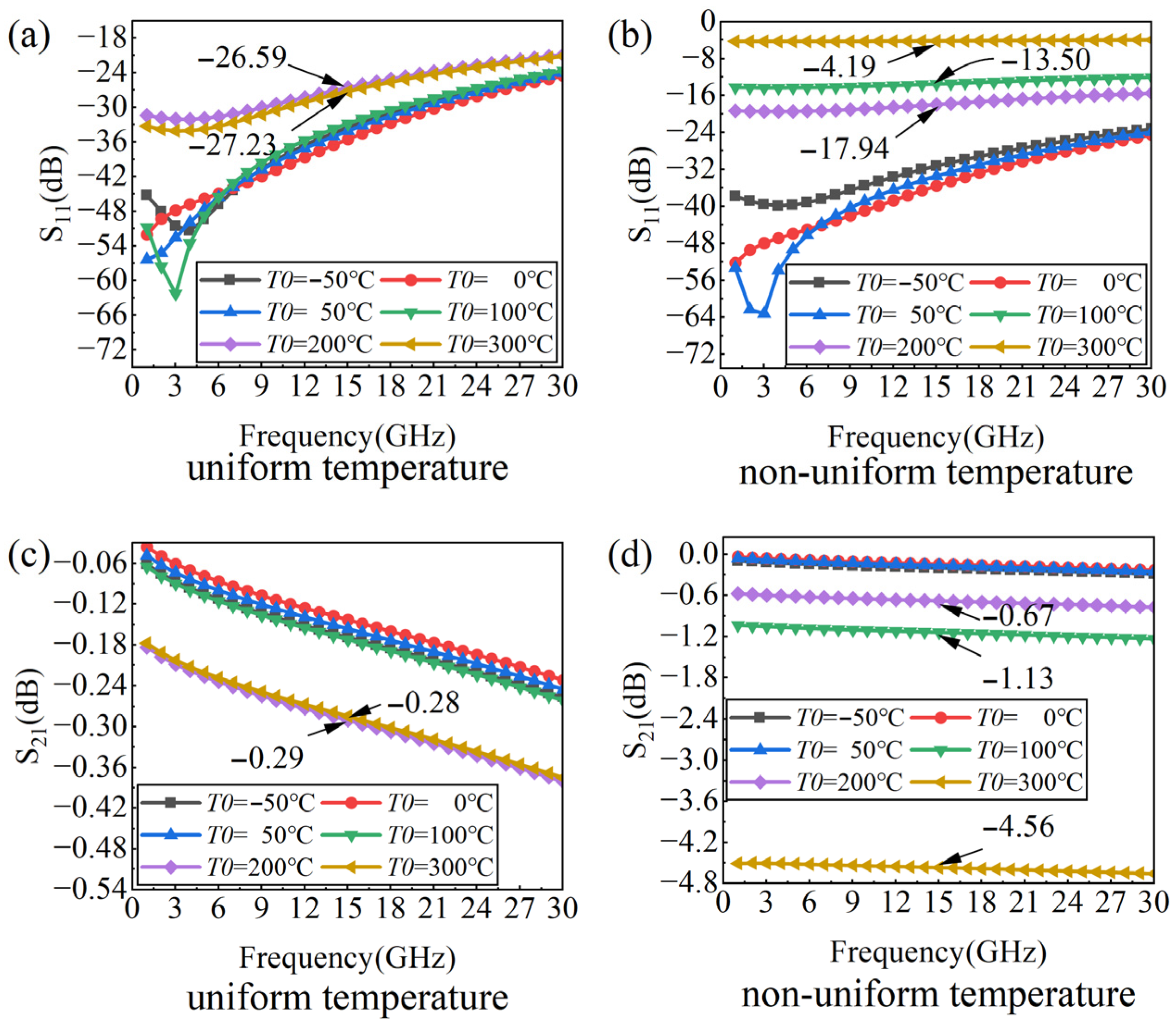
In industrial equipment applications, systematic studies have been carried out to explore the effects of extreme temperatures on device performance. The temperature range in this study spans from −50 °C to 300 °C, designed to investigate the response characteristics of the transmission line model under different thermal conditions. As shown in Figure 5a,c, under uniform temperature conditions, the scattering characteristics at the center frequency show minimal change when the temperature is increased from −50 °C to 300 °C in steps of 50 °C. However, when the temperature exceeds 200 °C, signal reflection increases and transmission efficiency decreases from 96.8% to 93.5%. In contrast, as shown in Figure 5b,d, under non-uniform temperature conditions—especially when the temperature exceeds 100 °C—the scattering characteristics at the center frequency change significantly. At 300 °C, the transmission efficiency drops to 35.0%, representing a 61.8% reduction compared with the baseline design obtained from single electric field analysis.
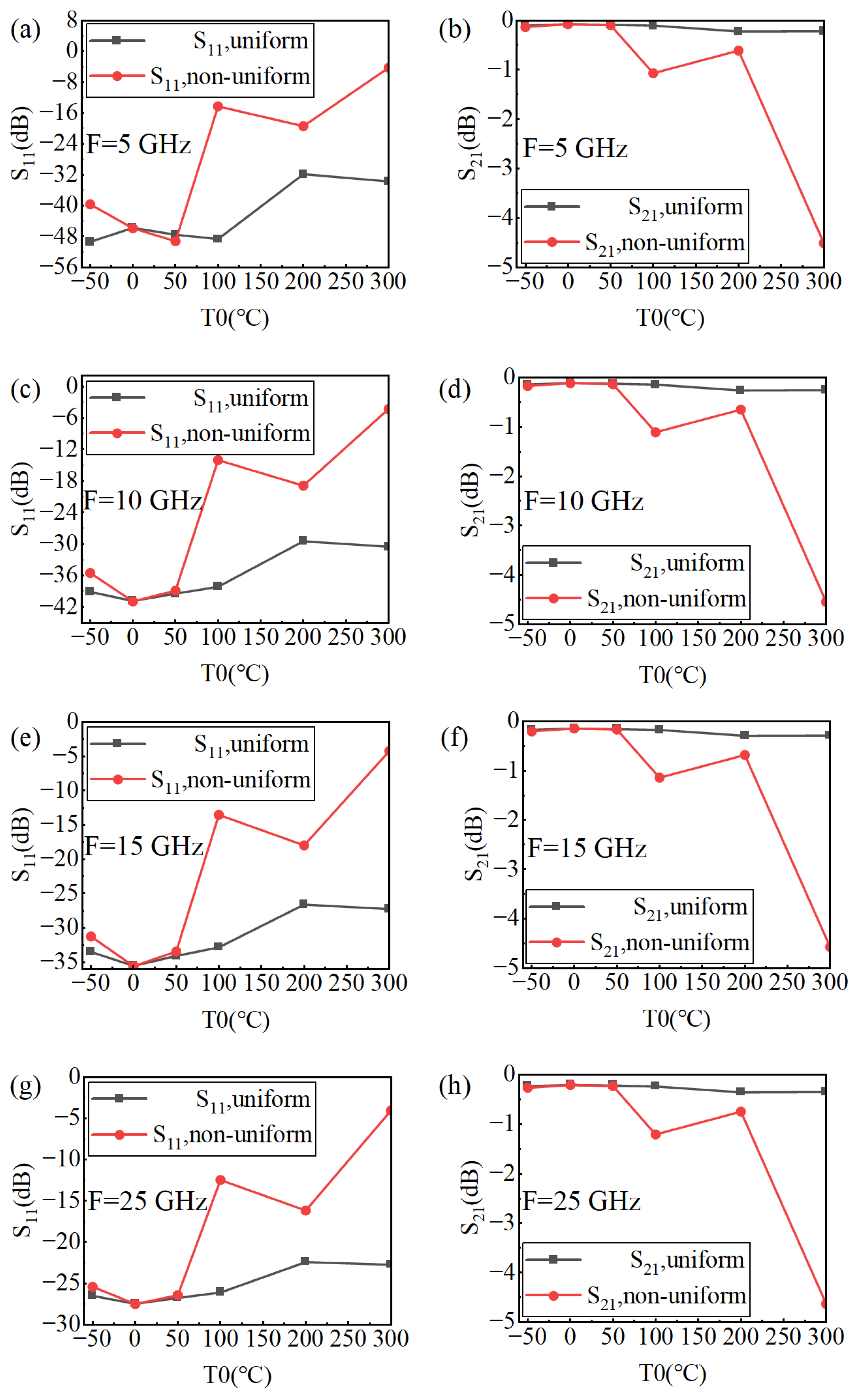
As shown in Figure 6a–h, at the same operating frequency, the relative variations caused by uniform and non-uniform temperature conditions are negligible when the temperature is below 50 °C. However, when the temperature exceeds 50 °C, non-uniform temperature conditions result in significantly larger scattering variations, more serious signal reflections, and lower transmission efficiency than uniform temperature conditions. This further demonstrates that non-uniform temperatures impair the reliability and stability of signal transmission within the system.

3.4. Improved Electromagnetic-Thermal Coupling Model

3.4.1. Scheme Design

To verify whether Scheme 1, a design obtained from electric field optimization, can be effectively applied under electromagnetic-thermal coupling conditions, a comparative analysis of different design parameters for the LTCC substrate transmission line is carried out under non-uniform temperature conditions with the temperature set to 300 °C. The detailed parameter settings are listed in Table 3.

3.4.2. The Effect of Different Schemes on Scattering Characteristics

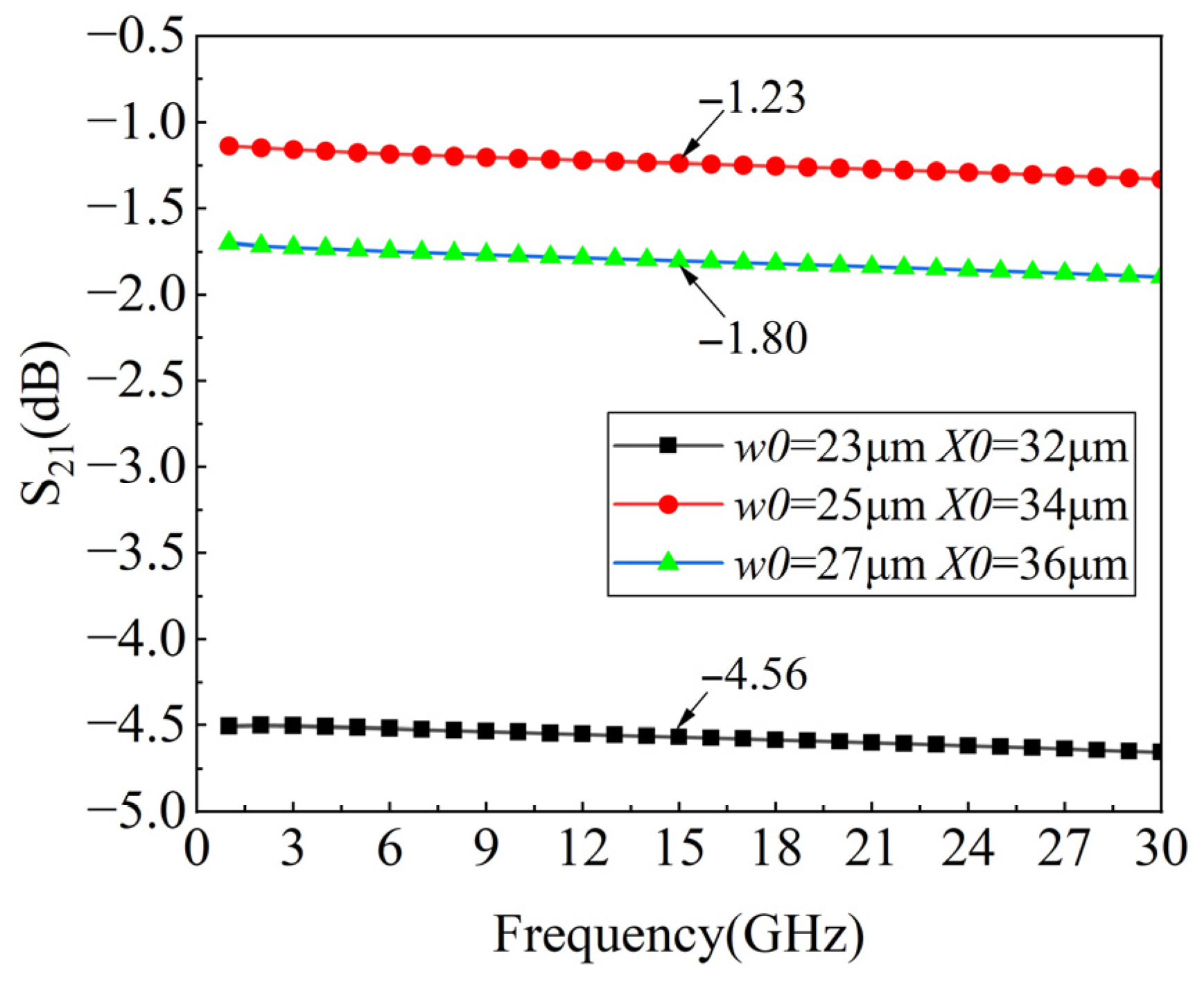
As shown in Figure 7, a comparative analysis of the S21 parameters for Schemes 1–3 shows that under 300 °C operating conditions, Scheme 2 exhibits significantly better transmission performance than the other schemes. Specifically, Scheme 2 maintains a transmission efficiency of about 75.3% at a center frequency of 15 GHz, nearly 2.1 times that of Scheme 1, which only achieves 35.0%. In addition, comparison with Scheme 3 indicates that structural parameters such as line width and spacing need to be fully optimized and verified under specific operating conditions. Overall, these results demonstrate that Scheme 1, selected only based on electric field performance, is not suitable for electromagnetic-thermal coupling working conditions.

4. Conclusions

This paper presents a simulation study of high-speed electromagnetic signals on LTCC substrates in SiP, focusing on the influence of uniform and non-uniform temperature fields (including those with local hotspots) on the S-parameters of transmission lines. The results show that temperature variations significantly affect signal transmission efficiency, and non-uniform temperature fields exert a significantly stronger influence on the electromagnetic performance of the device than uniform temperature fields. Under 300 °C operating conditions, Scheme 1 achieves a transmission efficiency of only 35.0% at the center frequency of 15 GHz, a 61.8% decrease compared with the optimal solution obtained from single electric field analysis. A comparative analysis of Schemes 1–3 indicates that structural parameters derived only from electric field simulation are not suitable for multiphysics coupling conditions. After structural optimization, the transmission efficiency of Scheme 2 is increased to about 75.3%, which is approximately 2.1 times that of Scheme 1. In addition, the amplitude of device performance fluctuations under high-temperature conditions is significantly larger than those under low-temperature conditions at −50 °C. These findings provide important reference data for subsequent high-temperature reliability design and experimental research.

Author Contributions

Methodology, X.L.; software, X.L.; validation, X.L.; data curation, X.L.; writing—original draft preparation, X.L.; writing—review and editing, L.C. and Z.L.; funding acquisition, L.C. and Z.L. All authors have read and agreed to the published version of the manuscript.

Funding

This research was funded by the Natural Science Foundation of China under Grant U2341223 (Ye Qisun Science Foundation).

Data Availability Statement

Data are contained within the article.

Conflicts of Interest

The authors declare no conflicts of interest.

Abbreviations

The following abbreviations are used in this manuscript:
LTCCLow temperature co-fired ceramic
SiPSystem-in-package
SBCScattering boundary conditions

References

  1. Li, J.H.; Ding, X.C. Research status and development trend of LTCC package technology. Electron. Packag. 2022, 22, 030205. [Google Scholar] [CrossRef]
  2. Miao, M.; Jin, Y.F. A new stage for microsystem integration-the integrated development of integrated circuits chips and system-level electronic packaging. Microelectron. Comput. 2021, 38, 1–6. [Google Scholar] [CrossRef]
  3. Coskun, A.; Eris, F.; Joshi, A.; Kahng, A.; Ma, Y.; Narayan, A.; Srinivas, V. Cross-layer co-optimization of network design and chiplet placement in 2.5-D systems. IEEE Trans. Comput.-Aided Des. Integr. Circuits Syst. 2020, 39, 5183–5196. [Google Scholar] [CrossRef] [Scilit]
  4. Wiss, E.; Jaziri, N.; Yuile, A.; Müller, J.; Wiese, S. Experimental Study on Reactive Joining Processes on LTCC Substrates; ESTC: Berlin, Germany, 2024; pp. 1–4. [Google Scholar] [CrossRef] [Scilit]
  5. Qin, Y.; Zhong, C.W.; Yang, H.Y.; Qin, T.Y.; Yuan, Y.; Tang, B.; Zhang, S. Enhanced thermal and mechanical properties of Li-Al-Si composites with K2O-B2O3-SiO2 glass for LTCC application. Ceram. Int. 2019, 45, 15654–15659. [Google Scholar] [CrossRef] [Scilit]
  6. Zhang, H.X.; Huang, L.; Wang, W.J.; Zhao, Z.G.; Zhou, L.; Chen, W.C. Massively parallel electromagnetic–thermal cosimulation of large antenna arrays. IEEE Antennas Wirel. Propag. Lett. 2020, 19, 1551–1555. [Google Scholar] [CrossRef] [Scilit]
  7. Wu, Q.Y.; Xu, Y.; Liu, N.; Zhang, M.W.; Liu, Q.H. Electrothermal transient co-simulation with domain decomposition method for 3-D complex integrated systems. IEEE Trans. Compon. Packag. Manuf. Technol. 2024, 14, 1374–1383. [Google Scholar] [CrossRef] [Scilit]
  8. Venkateswarlu, S.; Mishra, S.; Oprins, H.; Vermeersch, B.; Brunion, M.; Han, J.H. Impact of 3-D integration on thermal performance of RISC-V mempool multicore SOC. IEEE Trans. Very Large Scale Integr. Syst. 2023, 31, 1896–1904. [Google Scholar] [CrossRef] [Scilit]
  9. Ma, X.N.; Xu, Q.Z.; Wang, C.H.; Cao, H.; Liu, J.Y.; Zhang, D.Q.; Li, Z.Q. An electrical-thermal co-simulation model of chiplet heterogeneous integration systems. IEEE Trans. Very Large Scale Integr. Syst. 2024, 32, 1769–1781. [Google Scholar] [CrossRef] [Scilit]
  10. Zhang, H.X.; Wang, Y.D.; Wang, Y.Y.; Bai, R.C.; Chen, Z. Review of simulation method of multiphysics coupling process in three-dimensional structures under high power microwave action. Chin. J. Radio Sci. 2024, 39, 852–869. [Google Scholar]
  11. Luo, B.; Meng, H.; Zhang, J.B.; Li, Q.Q. Design and Simulation of Miniaturized Filters in the 5G Frequency Band; ICFTIC: Qiangdao, China, 2023; pp. 713–716. [Google Scholar] [CrossRef] [Scilit]
  12. Pourzadi, A.; Adibi, A.; Mousavi, S.H.; Kouki, A. A fast technique for realization of lumped-element values into 3-D physical layout on LTCC. IEEE Trans. Compon. Packag. Manuf. Technol. 2021, 11, 1497–1505. [Google Scholar] [CrossRef] [Scilit]
  13. Payne, K.; Xu, K.; Choi, J.H.; Lee, J.K. Multiphysics analysis of plasma-based tunable absorber for high-power microwave applications. IEEE Trans. Antennas Propag. 2021, 69, 7624–7636. [Google Scholar] [CrossRef] [Scilit]
  14. Ma, R.; Liang, J.; Zhang, B.; Fu, X. Design and Analysis of a Miniaturized LTCC Bandpass Filter for 5G Millimeter-Wave Applications; ICMMT: Bejing, China, 2024; pp. 1–3. [Google Scholar] [CrossRef] [Scilit]
  15. Yildiz, Ö.F.; Pathé, N.; Bochard, M.; Yang, C.; Schuster, C. Introducing functional via structures to low temperature cofired ceramics: How to optimize reliably and efficiently. IEEE Electromagn. Compat. Mag. 2021, 10, 35–45. [Google Scholar] [CrossRef] [Scilit]
  16. Ge, P.; Zhu, H.R.; Sun, Y.F. Wideband Bonding Wire Compensation Structure Design and Electric-Thermal Coupling Analysis for Chip Package; APMC: Bali, Indonesia, 2024; pp. 1284–1286. [Google Scholar] [CrossRef] [Scilit]
  17. Lu, T.J.; Jin, J.M. Electrical-thermal co-simulation for analysis of high-power RF/microwave components. IEEE Trans. Electromagn. Compat. 2017, 59, 93–102. [Google Scholar] [CrossRef] [Scilit]
  18. Yang, Z.L.; Zhu, H.; Zhou, L.Y.; Zhao, W.Y.; Huang, W. 2.5D microsystem multiphysics coupling simulation and optimization. Microelectron. Comput. 2022, 39, 121–128. [Google Scholar] [CrossRef]
  19. Feng, Q.; Tang, M.; Fu, G.; Mao, J. Fast Transient Thermal Simulation of 2.5-D Packages on Through Silicon via Interposer; SPI: Turin, Italy, 2016; pp. 1–4. [Google Scholar] [CrossRef] [Scilit]
  20. Yi, D.; Tang, L.; Tang, M.C.; Wei, X.C.; Li, E.P. Ultrathin, electrically small noise suppression sheet for microwave cavities of 3-D integrated circuits: Design methodology and realization. IEEE Trans. Microw. Theory Tech. Pap. 2022, 70, 1157–1168. [Google Scholar] [CrossRef] [Scilit]
  21. Zhan, Q.; Fang, Y.; Zhuang, M.; Yuan, M.; Liu, Q.H. Stabilized DG-PSTD method with nonconformal meshes for electromagnetic waves. IEEE Trans. Antennas Propag. 2020, 68, 4714–4726. [Google Scholar] [CrossRef] [Scilit]
  22. Sun, B.; Wang, Y.; Feng, H.; Chung, E.; Yin, W.Y.; Zhan, Q. Fast uncertainty quantification by sparse data learning from multiphysics systems. IEEE Trans. Microw. Theory Tech. 2023, 71, 4267–4281. [Google Scholar] [CrossRef] [Scilit]
  23. Lei, Y.X.; Yang, Y.; Bai, X.Y.; Liu, K.; Gao, B. Multi-Physical Field Simulation of Nonlinear High-Voltage Ceramic Capacitor Based on COMSOL; SPIES: Beijing, China, 2022; pp. 138–143. [Google Scholar] [CrossRef] [Scilit]
  24. Zhang, L.Y.; Zhang, Y.F. Simulation on Heat Transfer of Microchannels and Thermal Vias for High Power Electronic Packages; ICEPT: Chengdu, China, 2014; pp. 508–510. [Google Scholar] [CrossRef] [Scilit]
Figure 1. Simulation structural model: (a) Structure of LTCC; (b) Detailed parameters.
Electronics 15 01668 g001
Figure 2. Boundary conditions for LTCC substrate in SiP.
Electronics 15 01668 g002
Figure 3. The scattering characteristics were simulated under different design parameter conditions: (a) S11 vary with w0; (b) S21 vary with w0; (c) S11 vary with X0; (d) S21 vary with X0; (e) S11 vary with d1; (f) S21 vary with d1; (g) S11 vary with r0; (h) S21 vary with r0.
Electronics 15 01668 g003
Figure 4. Scattering characteristics simulated of Scheme 1: (a) S11; (b) S21.
Electronics 15 01668 g004
Figure 5. Scattering characteristics under different temperature conditions: (a) Value of S11 under uniform temperature; (b) Value of S11 under non-uniform temperature; (c) Value of S21 under uniform temperature; (d) Value of S21 under non-uniform temperature.
Electronics 15 01668 g005
Figure 6. Scattering characteristics vary with temperature under uniform and non-uniform temperature conditions: (a,b) F = 5 GHz; (c,d) F = 10 GHz; (e,f) F = 15 GHz; (g,h) F = 25 GHz.
Electronics 15 01668 g006
Figure 7. Comparison of S21 parameter results for different design schemes at 300 °C.
Electronics 15 01668 g007
Table 1. Parameter values of LTCC substrate in SiP.
ComponentsL × W × H/(μm)ComponentsR × S/(μm)H/(μm)L × W/(μm)
Substrate A900 × 900 × 100TCVr0 × X060/17/33/20/
Substrate B800 × 800 × 60Transmission line/ × X0d1300/200/225/100 × w0
Polyimide900 × 900 × 22Padsr1 × X01/
Table 2. Material parameters for LTCC substrate in SiP.
ParameterDuPont 951PolyimideCopper
Relative permittivity7.53.51
Relative permeability111
Electrical conductivity/(S·m−1)005.998 × 107
Young’s modulus/(GPa)1203110
Poisson’s ratio0.240.250.35
Thermal conductivity/(W·(m−1 × K−1))3.30.2400
Heat Capacity/(J·(kg−1 × K−1))8001000385
Thermal expansion coefficient/(K−1)5.8 × 10−630 × 10−617 × 10−6
Density/(g·cm−3)3.11.58.96
Table 3. Design schemes for different parameters in LTCC substrate in SiP.
Parameter Scheme 1 Scheme 2 Scheme 3
Transmission line width (w0)23 μm 25 μm27 μm
Transmission line spacing (X0)32 μm 34 μm36 μm
Transmission line height (d1)12 μm12 μm12 μm
TCV radius (r0)11 μm11 μm11 μm
Pad radius (r1)12 μm12 μm12 μm
Disclaimer/Publisher’s Note: The statements, opinions and data contained in all publications are solely those of the individual author(s) and contributor(s) and not of MDPI and/or the editor(s). MDPI and/or the editor(s) disclaim responsibility for any injury to people or property resulting from any ideas, methods, instructions or products referred to in the content.