
Article

Metalized Stereolithography 3D-Printed Rectangular Waveguide Components for Terahertz Radiation

1
Center for Advanced Laser Technology, Hebei University of Technology, Tianjin 300401, China
2
Hebei Key Laboratory of Advanced Laser Technology and Equipment, Tianjin 300401, China
3
Innovation and Research Institute of Hebei University of Technology in Shijiazhuang, Shijiazhuang 050299, China
4
Ceyear Technologies Co., Ltd., Qingdao 266555, China
*
Author to whom correspondence should be addressed.
Electronics 2026, 15(8), 1651; https://doi.org/10.3390/electronics15081651
Submission received: 13 March 2026 / Revised: 9 April 2026 / Accepted: 13 April 2026 / Published: 15 April 2026
(This article belongs to the Special Issue THz Sensing Systems and Components for Industrial Applications)

Abstract

Rectangular waveguides, serving as a standardized versatile platform for manipulating terahertz radiation within controlled environments, have been extensively employed across a broad range of terahertz systems. However, conventional fabrication methods encounter significant challenges in realizing such submillimeter-scale structures within a monolithic integration, particularly when subwavelength features or intricate geometries are incorporated for advanced functionalities. In this work, we propose a fabrication route integrating stereolithography 3D printing and electroless plating, and demonstrate its broad applicability, intrinsic benefits and limitations through the realization of various high-performance D-band terahertz rectangular waveguides and antennas. The resulting rectangular waveguides achieve an insertion loss below 0.3 dB and a return loss above 15 dB across the D-band, while remaining stable across extreme temperatures (−50 °C to 150 °C) and offering a weight reduction of over 60%. A monolithically fabricated smooth-walled conical horn antenna exhibits beam-shaping characteristics that closely align with theoretical expectations. Attempts on corrugated horn antennas in conventional design reveal degraded performance, primarily arising from the inherent staircase effect associated with 3D printing. A novel design featuring obliquely oriented corrugations is developed, effectively mitigating uncontrolled deformation in periodic subwavelength features. Compared with the classical corrugated design (θ = 90°), the proposed obliquely oriented corrugations (θ = 30°) improve the agreement between experimental and theoretical radiation patterns, reducing the gain deviation from 1.45 dB to less than 0.5 Db—a quantitative improvement of over 60% in pattern fidelity. We believe that this fabrication route together with the process-adaptive design paradigm establishes a robust technical foundation for realizing high-performance, lightweight, and design-flexible terahertz waveguide components and holds significant promise for advancing the development of next-generation integrated terahertz systems.

1. Introduction

The terahertz wave, spanning 0.1–10 THz, is distinguished by the unique properties of an unregulated broad band, strong penetration through many optically opaque materials, and access to numerous molecular spectral fingerprints, establishing it as an advanced technology for next-generation high-speed wireless communications, non-destructive imaging, and spectroscopy [1,2]. Rectangular waveguides, a design with origins in the early 20th century for microwave technologies, are currently indispensable in the terahertz band, serving as standardized platforms for waveguiding, interconnecting, and chip packaging [3,4,5]. Their commercial success is attributed to low transmission loss, reliable single-mode operation, structural robustness and simplicity, and tightly controlled mode field distribution. Design flexibility also enables advanced signal processing functions, highlighting their versatility in terahertz systems [6,7,8]. Horn antennas, which convert waveguide modes into directional, high-gain free-space radiation over a broad bandwidth, are key components for long-range terahertz wireless communications [9,10]. Beyond the basic design, engineered variants such as corrugated and lens horn antennas offer advanced capabilities like polarization control and radiation pattern shaping [11,12], meeting the stringent demands of co-channel signal utilization and power efficiency in terahertz links.
However, in terms of the stand-alone rectangular waveguide component itself, while terahertz ones typically adhere to the well-established design for microwaves, they require drastically tighter manufacturing tolerances. This is driven by the submillimeter cross-sectional dimension of the through hole, i.e., the structure enabling wave guidance, together with its integrated subwavelength features required for certain components (e.g., resonators in waveguide filters [13]). Conventional subtractive methods such as CNC machining face significant challenges in fabricating high-precision terahertz waveguide components due to limitations in tool reach and accuracy, leading to dimensional errors that degrade waveguide transmission performance and hinder miniaturization and integration. High-resolution microfabrication techniques like LIGA and deep silicon etching [14] have been successfully applied to higher-frequency terahertz components (e.g., antennas at 850 GHz [15]), but suffer from high costs, poor structural stability, and integration difficulties. Selective laser sintering and melting (SLS/SLM) [16] have enabled fully metal components such as horn antennas [17], yet the limited spatial resolution of commercial metal printers introduces dimensional errors and surface roughness that cause performance gaps even in the lower-terahertz band. In contrast, stereolithography (SLA) 3D printing offers tens-of-micrometer resolution and, combined with metallization, has proven viable for fabricating terahertz waveguides [18,19,20,21]. While this approach promises to overcome longstanding limitations across multiple fields, further work is needed to verify its universal applicability, optimize processes, evaluate multi-physical performance in complex structures, and develop design strategies to compensate for fabrication imperfections.
In this work, we propose a diverse set of terahertz rectangular waveguide components in monolithic metalized 3D prints and reveal the broad applicability of the fabrication route that combines SLA 3D printing and electroless plating by demonstrating their excellent electromagnetic performance. Details of the manufacturing process and the physical properties of these components are presented. Specifically, waveguiding performance of D-band rectangular waveguides, including insertion and return losses, resilience under extreme thermal conditions, and performance in high-speed data transmission, is validated. Expanding on this, we develop terahertz horn antennas within monolithic builds, ranging from a featureless conical one to corrugated designs containing periodic subwavelength features. To address the inherent limitations of 3D printing in accurately reproducing periodic subwavelength features, we develop a corrugated horn antenna with obliquely oriented corrugations. Compared with prior demonstrations of metalized 3D-printed terahertz components, this process-adaptive design uniquely mitigates the staircasing effect inherent to layer-by-layer fabrication, enabling monolithic printing of subwavelength features with precision in a single shot. By mitigating fabrication-induced geometric distortion, this process-adaptive design enhances geometric fidelity while preserving the desired radiation control performance. Collectively, our results establish the proposed fabrication route as a versatile alternative to conventional manufacturing, enabling lightweight, high-performance terahertz devices with unparalleled design flexibility.

2. 3D-Printed Terahertz Rectangular Waveguides

2.1. Additive Manufacturing of Terahertz Rectangular Waveguides

Different from microwave ones, rectangular waveguides designed for terahertz radiation exhibit a much higher aspect ratio, i.e., the ratio between the length and the cross-sectional dimension of the hollow-core channel, which is on the order of centimeters and sub-millimeters, respectively. It renders subtractive manufacturing (e.g., CNC machining) no longer an effective technique to fabricate the desired structure. In most cases, post-processing of discretely manufactured complementary parts is required; however, misalignment during assembly could lead to degraded waveguiding performance. In contrast, stereolithography 3D printing enables the monolithic production of the substrate of rectangular waveguide components with ease and precision, even for the ones containing deeply subwavelength features. Considering the minimal penetration depth of the THz band into most metals [22], subsequent surface metallization of the hollow-core channel could allow these 3D prints, made from cured photopolymer resin, to function comparably to those of all-metal devices in waveguiding applications. Furthermore, such a fabrication route imparts a lightweight nature to the waveguide components due to the low density of resin, thus making them perfectly suitable for weight-sensitive applications (e.g., interconnects in satellites).
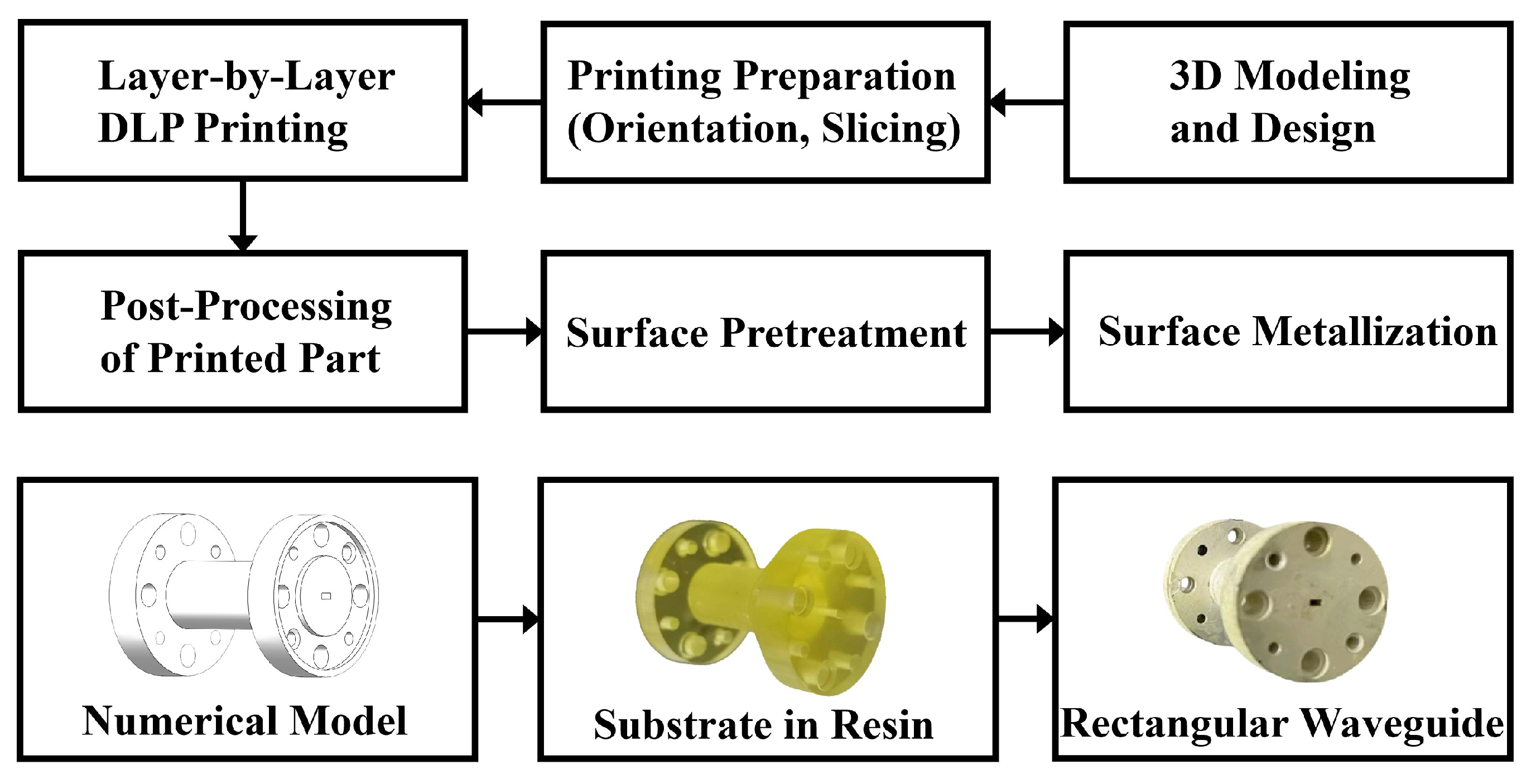
The fabrication route of the proposed terahertz rectangular waveguide is illustrated in Figure 1. The process begins with 3D model design and optimization using computer-aided design software. Subsequently, DLP printing is performed to adjust the printing orientation and generate slice layers. After printing, the part is rinsed in isopropanol to remove uncured resin and post-cured under UV light. Specifically, dielectric substrates of terahertz rectangular waveguide components were obtained by a desktop digital light processing (DLP) 3D printer (Titan 3, MicroSLA Inc., Dublin, CA, USA) in this work. The XY-resolution and layer thickness were set to 25 μm and 10 μm, respectively. The cured photopolymer resin, which is mainly composed of oligomers and reactive diluent monomers, was measured with a density of 1.15 g/cm3 after thermal curing (160 °C, 3 h). It was characterized with a Shore D hardness of 86 (ASTM D2240) [23], a Young’s modulus of 2720 MPa (ASTM D638) [24] and a flexural modulus of 2510 MPa (ASTM D790) [25], indicating satisfactory structural robustness of 3D-printed rectangular waveguide components. Thereafter, surface pretreatment was conducted, including surface roughening treatment and sensitization, to enhance surface activity and ensure strong adhesion between the resin substrate and the metallic layer. The roughening treatment created microscale roughness, followed by sensitization in a stannous chloride solution at room temperature. Each step was followed by thorough rinsing with deionized water. Finally, electroless silver plating was carried out using a dynamic liquid-phase deposition technique with peristaltic pumps. Unlike traditional immersion plating where the entire structure is submerged, this method effectively mitigates the air barrier effect that impedes solution penetration into high-aspect-ratio cavities. By precisely regulating the solution composition, flow rates, and process sequence, a uniform metallic coating formed via the redox reaction. This dynamic process maintained a consistent concentration of reactants along the entire channel, enabling uniform coating thickness on the inner walls. After deposition, the waveguide was rinsed with deionized water and dried. This standardized procedure ensures high reproducibility and uniform coating even in high-aspect-ratio structures.
Given the rapid advancement and prototype-level deployment of low-frequency terahertz systems (e.g., 6G backhaul links, non-destructive inspection, and vehicle-mounted radar [26]), the D-band (110–170 GHz, corresponding to wavelengths of 1.76–2.73 mm) was selected as the operational frequency range to demonstrate the capability of the proposed rectangular waveguide components.

2.2. Characterization of 3D-Printed Rectangular Waveguide

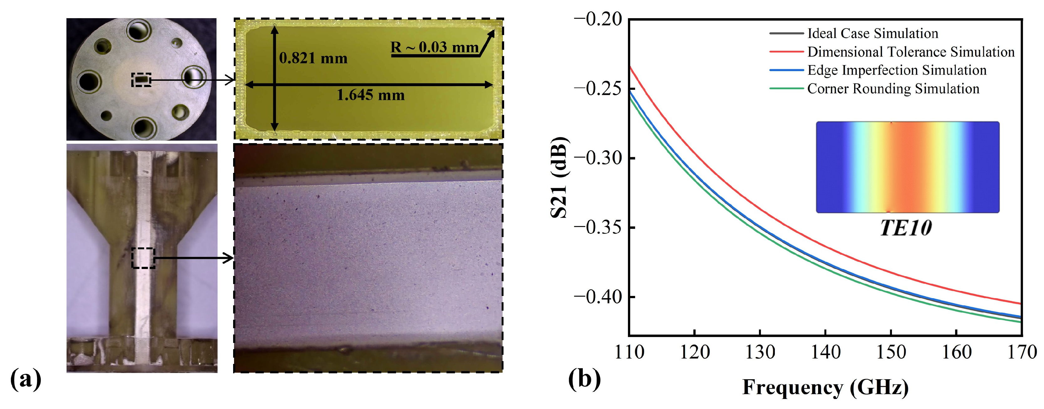
A 1-inch-long D-band rectangular waveguide fitted with standard UG-387/U [27] flanges for inter-device connections was fabricated as an integrated structure in a single shot (see Figure 2a). Compared to the all-metal counterparts with a weight of ~50 g, the lower density of photopolymer resin allows 3D-printed ones to achieve over 60% mass reduction. The cross section of the hollow core, measured as 1.632 mm × 0.809 mm at the end facet, features a small geometrical deviation from the ideal design (1.651 mm × 0.826 mm). Besides, due to inherent defects associated with 3D printing—such as suboptimal layout of support structures, release film degradation after prolonged use, limited printing resolution, as well as stress relaxation in the post-curing process—deformations such as edge rounding at right-angle corners (measured curvature radius of ~0.03 mm) and localized micro-defects along the hollow-hole channel (microstructured protrusions or depressions at the surface) were also observed. To quantitatively assess the impact of the aforementioned geometric deviations on the electromagnetic performance, a numerical simulation using the finite element method on the eigenmode supported by the rectangular waveguide was conducted. The hollow core was modeled as air, and an impedance boundary condition incorporating the Drude–Lorentz model was applied to the boundary to represent the metallic surfaces. A mode analysis was conducted. A fine mesh with maximum and minimum element sizes constrained to λ/5 and λ/10, respectively, was adopted to ensure solution accuracy, and a single-variable approach was adopted to isolate the effect of each geometric feature (see Figure 2b). One can see that the cross-sectional shrinkage leads to a lower modal loss of the supported TE10 mode, thus enabling a slight increase in the S21 value, but at the cost of a reduction in the cutoff frequency. Edge rounding imposes a negligible perturbation to the electromagnetic field distribution, while micro-defects result in localized mode disturbances and a marginal loss increment. The aforementioned 3D-printing-induced defects collectively demonstrate a small impact on guided-mode field distribution (Figure 2b inset) and transmission loss within the operational band.
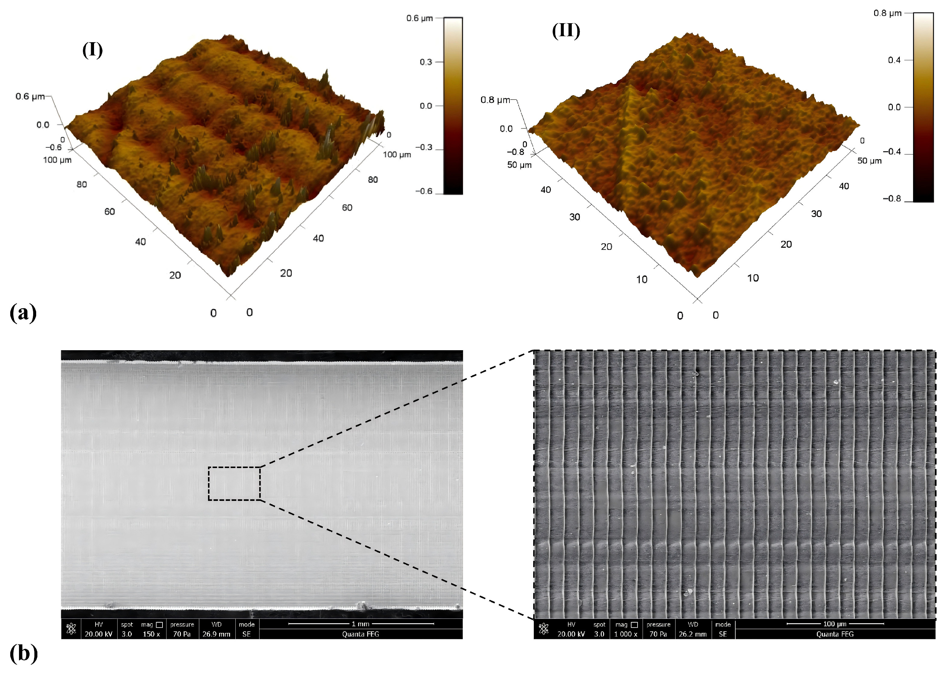
The surface morphology of the hollow-core channel was characterized by atomic force microscopy (AFM, Asylum Research MFP-3D), revealing the surface roughness and the thickness of the deposited silver layer. Due to the finite Z-axis printing resolution, periodic undulations with a pitch of approximately 10 μm—corresponding to the printing layer thickness—were observed on the waveguide surface. The arithmetic average roughness (Ra) was measured to be 53.463 nm and 83.906 nm for the structure before and after metallization, respectively (Figure 3a). The silver layer deposited onto the resin substrate was measured with a thickness of hundreds of nanometers, an order of magnitude greater than the skin depth at 140 GHz, thus enabling 3D printing with waveguiding performance similar to that of their metal counterparts. However, the effective conductivity of the plated silver layer was measured to be 4.24 × 10⁷ S/m [28], which is slightly lower than that of bulk silver, likely due to surface roughness and surface oxidation. Despite this reduction, conductivity remains sufficiently high to support waveguiding. Cross-sectional SEM imaging of the waveguide channel was performed to assess the uniformity of the deposited silver layer (see Figure 3b for the wide-wall cross-section of the rectangular waveguide channel after silver plating). The surface of the cross-section appears flat with straight edges, and the silver layer exhibits good adhesion to the resin substrate without observable delamination or cracking. Periodic striations resulting from the layer-by-layer 3D printing process are clearly visible, with a spacing corresponding to the printing layer thickness. Therefore, beyond the D-band implementation, we believe that this fabrication route is scalable to higher terahertz frequencies. The measured post-metallization surface roughness (Ra ≈ 84 nm) is well below λ/30 (approximately 10 μm) at 1 THz [29], indicating that frequencies up to 1 THz are theoretically attainable with improved micrometer-scale printing resolution. From a dimensional perspective, the geometric fidelity of the SLA process yields dimensional deviations within 15 μm, meeting the tolerance requirements for terahertz waveguide components across this frequency range.
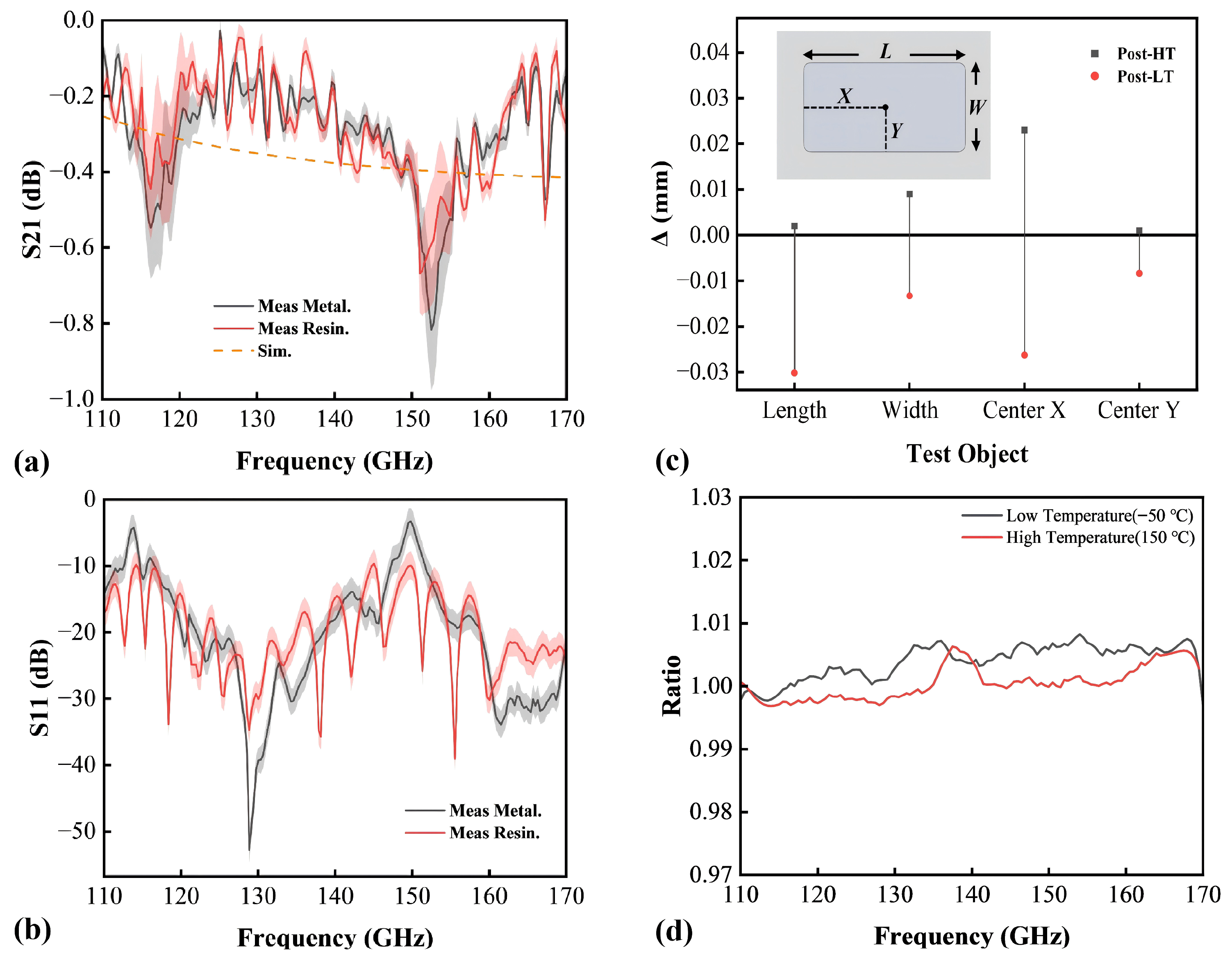
The metallic 3D-printed rectangular waveguide, together with an all-metal one as a control, was characterized using a vector network analyzer (CEYEAR 3674E). Prior to measurement, a standard through-reflect-line (TRL) calibration was performed to eliminate systematic errors. Measurement uncertainties were small, primarily stemming from the intrinsic stability of the VNA source (±0.03 dB) and negligible residual multipath scattering in the laboratory environment. Three independent measurements were performed after reconnecting the waveguide each time. The standard deviation at each frequency point was calculated to quantify the repeatability of the measurement. The overall uncertainty was estimated by combining this statistical variation with the instrument source stability (±0.03 dB) and potential environmental losses through a root-sum-square estimation. The resulting uncertainty range is visualized as shaded error bands in the curves. The experimental results indicate consistent S21 and S11 across the target frequency band. Specifically, the insertion loss remains below 0.3 dB (see Figure 4a), and the return loss is above 15 dB (see Figure 4b). Contrary to expectations, several ripples were observed in the measured curves, particularly in the S21 parameter. This fluctuation mainly originates from non-ideal contact between the waveguide and the testing system. Although the waveguides were connected using standard UG-387/U flanges to ensure coaxial alignment, residual surface roughness and slight end-face tilt at the interface can still cause minor impedance discontinuities and contribute to the observed fluctuations. Furthermore, as a critical enabling component for terahertz radiation propagation, the temperature adaptability of waveguides plays a decisive role in ensuring the stability of terahertz systems for practical applications. To evaluate this, the fabricated waveguides were subjected to temperature cycling tests (−50 °C and 150 °C, 12 h/cycle), with end-facet dimensions and transmittance recorded before and after the test. Experimental results demonstrate that dimensional deviations due to thermal expansion remain below 0.05 mm (see Figure 4c), while the transmittance ratio remains unity within the desired band in general (see Figure 4d), indicating virtually unchanged performance.
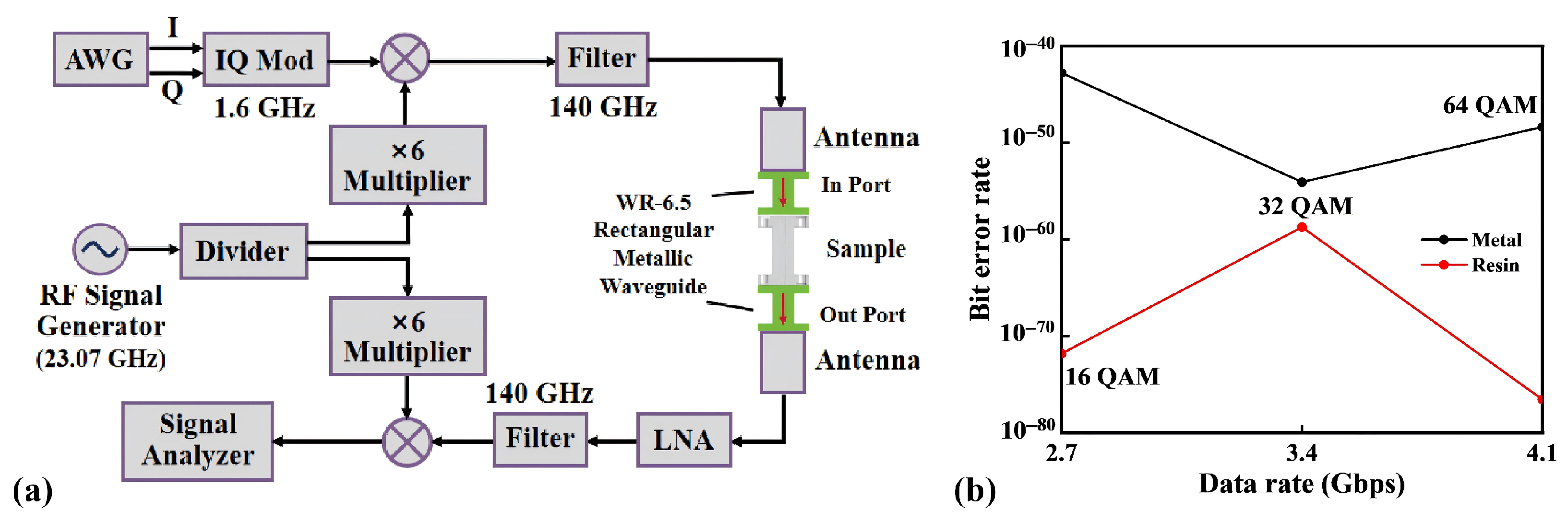
Further evaluation of the data transmission function was conducted using the terahertz communication system illustrated in Figure 5a. Based on a 140 GHz carrier wave, data streams were transmitted by switching sub-channels within a 1.75 GHz flat passband using QAM modulation formats. The signal propagating through rectangular waveguides was acquired and processed by a signal analyzer for demodulation and bit error rate (BER) measurement [30]. The experimental results demonstrate that the measured BER under Gbps-level data rates was far below the clear-channel transmission threshold (10−12, see Figure 5b). It reveals that the 3D-printed rectangular waveguide can support ultra-high data-rate signal transmission while performing comparably to its fully metal counterparts. However, the maximum data rate has not been identified in experiments due to the limited operating bandwidth of the current communication system.

3. 3D-Printed Conical Horn Antennas

A conical horn antenna, built upon a rectangular waveguide, offers one of the simplest solutions for bidirectional conversion between free-space radiation and guided waves within devices. Featuring moderate gain and a broad operational band, it is among the most widely used components in both photonic- and electronic-based terahertz systems for various applications. For instance, when fitted with a terahertz transmitter, the directional beam emitted through its flared aperture structure could enable long-range wireless links even under limited output power conditions [31]. However, its implementation in the terahertz regime inherits the key limitation of rectangular waveguides, i.e., the difficulty in realizing high-precision monolithic fabrication. The misalignment between independently CNC-machined discrete components in the post-assembly process, which is formidably challenging (if not impossible) to avoid, could lead to degraded gain and even failure in specific functions for antennas with complex structures. In contrast, the aforementioned fabrication route can circumvent such process-related challenges and holds promise for endowing the fabricated antennas with the desired performance as intended in design. 3D-printed D-band antennas were demonstrated as follows to illustrate the adaptability and limitations of this fabrication route.

3.1. Terahertz Conical Horn Antenna with Smooth Surface

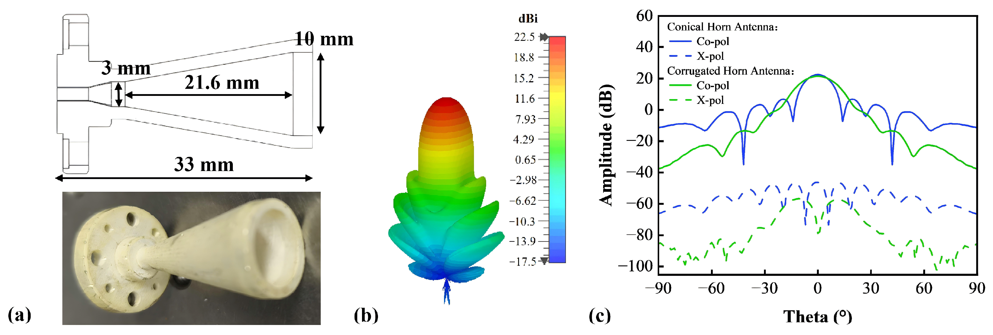
A conical horn antenna consisting of a WR-6.5 rectangular waveguide feed fitted with a UG-387/U flange, a 2.92 mm long rectangular-to-circular transition segment, a 3 mm diameter circular waveguide, as well as a conical horn section with 21.6 mm axial length and 10 mm aperture diameter was developed (see Figure 6a). Numerical simulations verify the high radiation efficiency of such a design across the D-band, with a far-field gain reaching 22.5 dBi and sidelobe levels below −10 dB at 140 GHz (see Figure 6b,c). Following the fabrication route shown in Figure 1, such a horn antenna was successfully fabricated as a monolithic metallic 3D-printed structure, exhibiting minimal geometrical deviation from the original design.
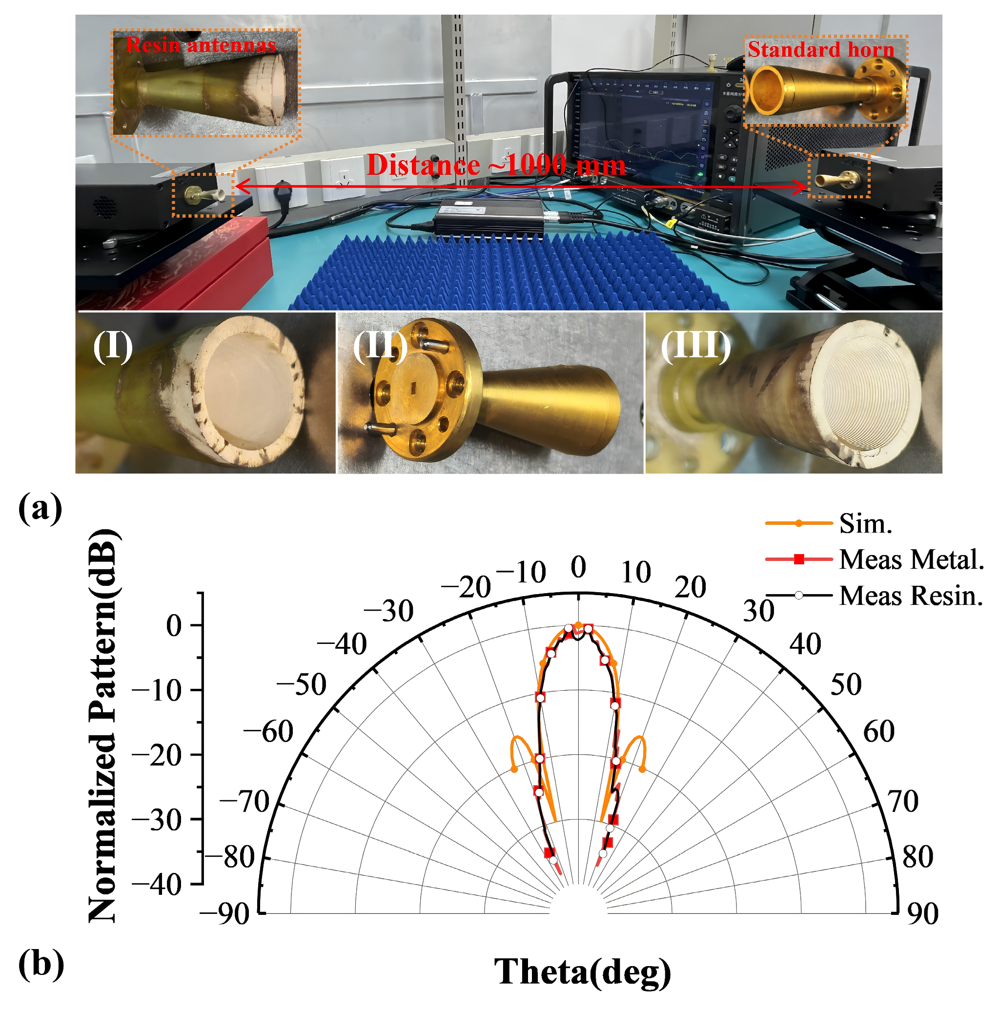
Together with its CNC-machined all-metal counterpart, the 3D-printed horn antenna was characterized using the experimental setup shown in Figure 7a. The antenna under test was mounted on a high-precision rotary stage and coaxially aligned with a standard-gain reference horn antenna (metallic conical horn) at a distance satisfying far-field conditions (approximately 1000 mm). Afterward, E-plane radiation patterns were recorded by rotating the antenna from −30° to +30° (see Figure 7b for the normalized result). Experiments found good agreement in the radiation pattern between our 3D-printed antenna and the metal reference at 140 GHz, with this trend persisting across the entire D-band. Further observation reveals that within this measurement range, the main lobe characteristics of the 3D-printed antenna show excellent agreement with the simulations, that is, the measured 3 dB beamwidth is 14.6°, which is very close to the simulated value of 15.2°. The small discrepancies in the sidelobe regions are mainly attributed to measurement uncertainties, including alignment errors and system calibration residuals. Based upon these experimental findings, one can conclude that the 3D-printed horn antenna can serve as a lightweight substitute for the all-metal ones, offering comparable beam-shaping performance.

3.2. Terahertz Corrugated Horn Antenna

Considering the decline in radiation efficiency and mode purity for conical horn antennas with increasing operating frequency, corrugated ones, incorporating periodic subwavelength corrugations along their inner walls and exhibiting superior radiation field distribution, have been adopted for certain terahertz applications [32]. Compared with the featureless horn antenna, the presence of the corrugations suppresses higher-order mode interference and enhances beam symmetry through surface current modulation and electromagnetic phase control, thus endowing the corrugated horn antenna with a higher gain and lower cross-polarization in most cases [33]. However, such microstructured corrugations—arranged along the axial direction of the flare with spatially varying depths and periods—are challenging to reproduce via CNC machining, even with costly infrastructures and expertise in processing. Additionally, despite offering a higher resolution, microfabrication techniques (e.g., deep reactive-ion etching and LIGA) are limited to corrugated horn antennas for the high-terahertz band due to constraints in compatible materials and achievable structural volume. In contrast, additive manufacturing techniques hold promise to replicate the desired overall architecture and intricate internal features, enabling integrated fabrication of terahertz corrugated horn antennas. Compared with all-metal counterparts produced by commercial selective laser melting 3D printers, corrugated horn antennas fabricated via an SLA 3D-printing-based fabrication route could achieve better surface finish and minor structural deformation.
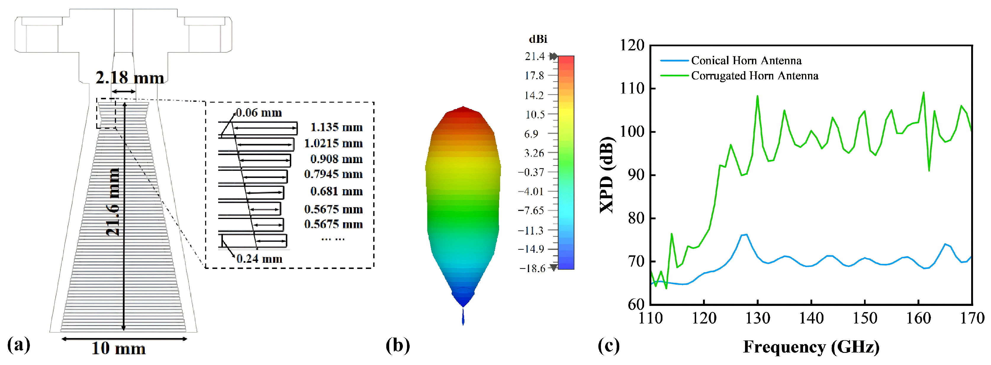
For the purpose of enabling a comparative performance analysis, a corrugated horn antenna sharing the same overall configuration as the abovementioned conical horn antenna (see Figure 6a) is demonstrated as follows. To achieve superior radiation performance, periodic corrugations were superimposed along both the TE11-HE11 mode converter and its connected linearly profiled flare sections (see detailed design in Figure 8a). The design follows classical principles of corrugated horn antennas [34,35,36]. Specifically, six grooves with a width of 0.24 mm and depths tapered from 1.1350 mm to 0.5675 mm are incorporated into the mode converter to facilitate the excitation of the hybrid HE11 mode while suppressing higher-order modes through impedance matching. Additionally, 0.3 mm period depth-tapered corrugations with groove and tooth widths of 0.24 mm and 0.06 mm, respectively, are implemented along the linearly profiled flare section. Such a design maintains a relative power ratio of 0.85:0.15 between TE11 and TM11 modes, thereby achieving a trade-off between beam symmetry and cross-polarization discrimination (XPD) in the antenna. Numerical radiation patterns reveal that compared with the featureless one, the corrugated horn antenna exhibits a larger beamwidth (16.3°), enhanced sidelobe suppression (~20 dB) and a higher beam circularity at 140 GHz (see Figure 6c and Figure 8b). In addition, an XPD improvement of over 25 dB is theoretically achieved across the D-band (see Figure 8c).
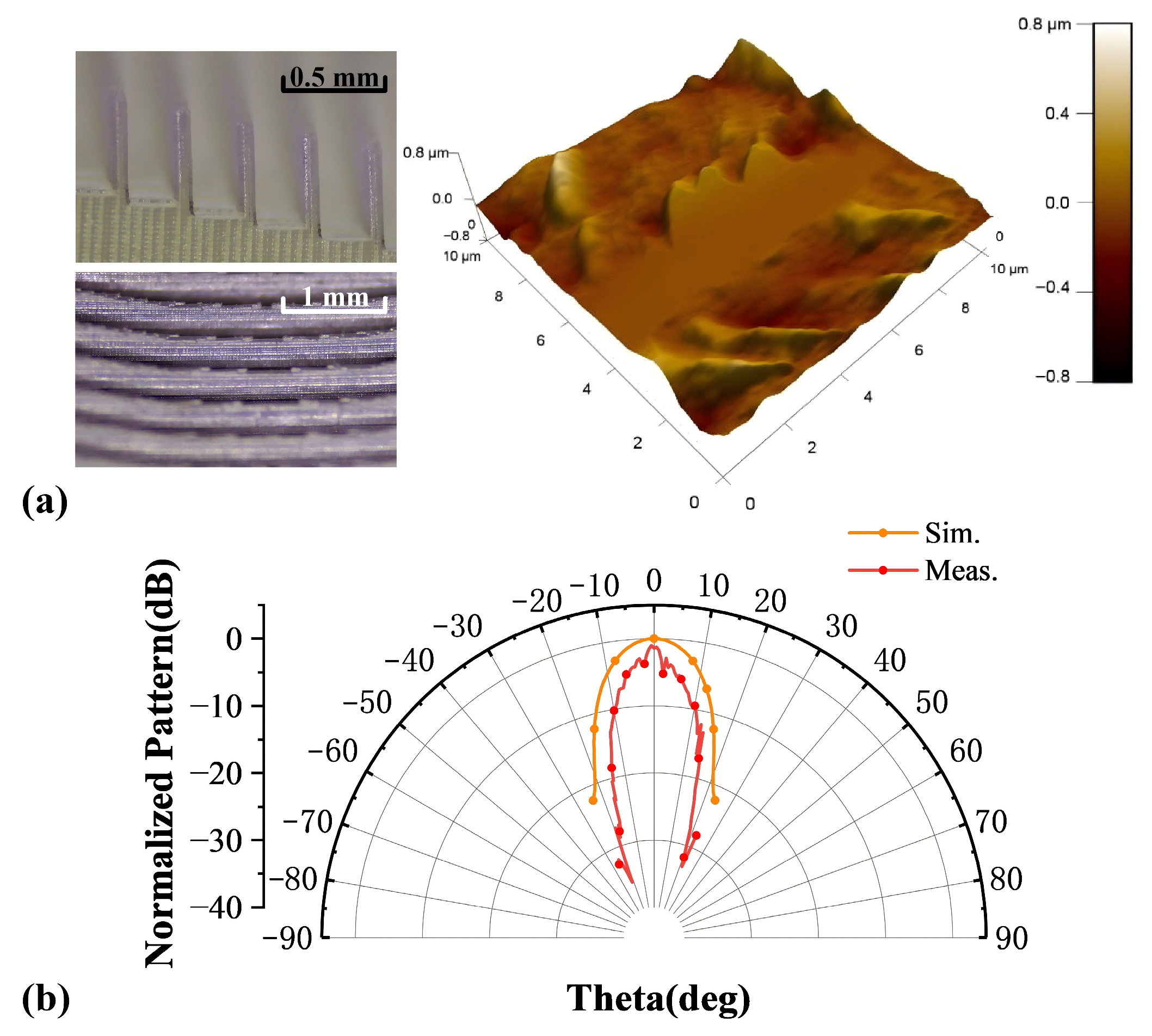
The fabrication and characterization of corrugated horn antennas were conducted using the same methodologies as those for the conical horn antenna (see Figure 1 and Figure 7a). It should be noted that, to avoid the need for adding supports between adjacent teeth and to ensure their structural integrity, the whole structure and the contained axis-perpendicular corrugations were printed with a tilt angle. One can observe that the 3D-printed subwavelength grooves exhibit a surface finish comparable to that of the rectangular waveguide (see Figure 3 and Figure 9a). However, when adopting this tilted printing orientation strategy, the inherent layer-staircase effect of 3D printing inevitably leads to pronounced microstructural defects on the fabricated subwavelength corrugations, such as incomplete groove profiles and localized burrs. These fabrication-induced imperfections disturb the periodic surface impedance distribution essential for supporting the balanced hybrid HE11 mode, inducing spurious mode conversion from the dominant HE11 into higher-order parasitic modes, thereby degrading modal purity. This results in increased cross-polarization levels, deteriorated radiation pattern symmetry, and reduced aperture efficiency, thus resulting in degraded performance relative to expectations. The return loss of a 3D-printed corrugated horn antenna was characterized as −16 dB at 140 GHz, approximately 10 dB higher than the numerical one. Besides, when normalized with the 3D-printed conical horn antenna, despite the fabricated corrugated one presenting a broader symmetrical beam radiation pattern without observable sidelobes, a lower gain was recorded (20 dBi), which is 1.45 dB lower than its numerical result (see Figure 9b).

3.3. Corrugated Horn Antenna with Tailored Subwavelength Features

To address the manufacturing limitations of classic corrugated horn antennas, inspired by [37], we propose a modified design incorporating intentionally tilted corrugation structures. This approach enables support-free monolithic printing in the vertical direction, thereby eliminating the stair-stepping artifacts inherent to tilted printing orientations. The resulting high geometric fidelity preserves the intended periodic surface impedance modulation, which in turn reduces cross-polarization levels and improves radiation pattern symmetry, enhancing overall antenna performance while simplifying the manufacturing process.
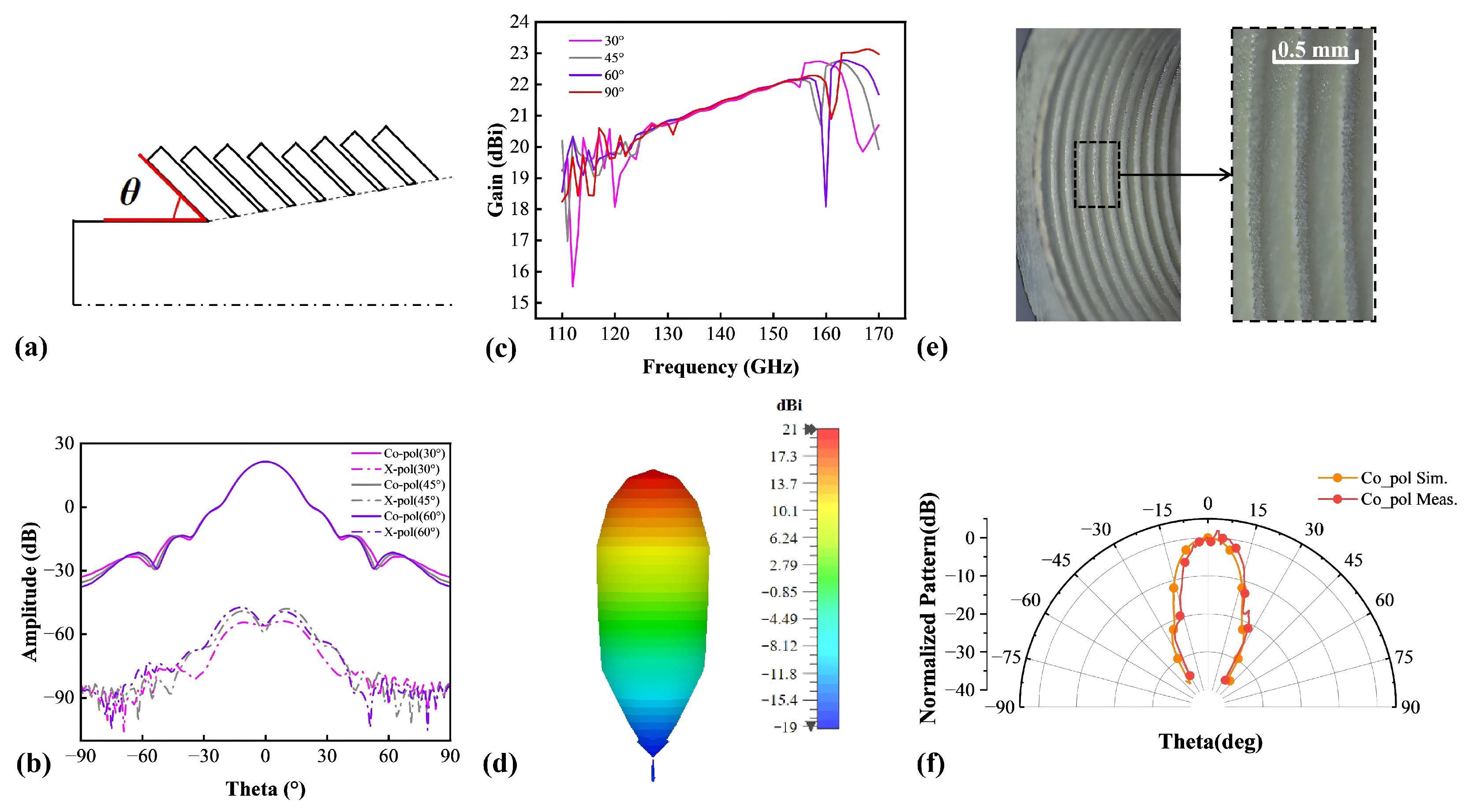
Figure 10a shows the schematic of periodical corrugations along the flare section, where tilt angle θ is defined as the angle between the teeth and the longitudinal axis (θ = 90° represents the corrugated horn antenna design in Figure 8a). With the other geometric parameters of the corrugated horn antenna design detailed in Section 3 held constant, numerical simulations were conducted for configurations with θ of 30°, 45°, and 60°. The results confirm that the electromagnetic performance remains largely insensitive to variations in θ, as shown in Figure 10b,c. To address the unavoidable gravitational effect during vertical printing, a corrugated horn antenna with a small θ (30°), despite exhibiting a gain reduction of approximately 0.45 dBi compared with the 90° one (see Figure 10d), was implemented following the fabrication route in Figure 1. The experimental results indicate that the obtained substrate exhibits periodical corrugations with fewer local micro-deformations and improved groove parallelism (see Figure 10e), enabling higher geometric fidelity relative to the ideal design compared to the one shown in Figure 9a.
The demonstrated 3D-printed corrugated horn antenna was characterized with a return loss (S11) below −20 dB across the D-band and a 3 dB beamwidth of 16.4° at 140 GHz. It is worth noting that the deviation between experimentally normalized and numerical gain remains below 0.5 dBi throughout the entire angular test range at 140 GHz (see Figure 10f). Such performance improvement over the classical 90° design highlights the suitability of 3D printing for reproducing horn antennas with such tilted corrugations. Nevertheless, the measured XPD (~40 dB) remains lower than the numerically predicted value. This discrepancy primarily arises from fabrication imperfections, such as residual non-circularity of the flare profile and minor structural deformations induced during post-curing and metallization. Such geometric defects disrupt the structural symmetry required for high polarization purity, thereby degrading the XPD. In contrast, the influence of environmental scattering was assessed by measuring free-space transmission under ambient conditions; the S21 parameter remained better than 0.2 dB across the D-band, indicating that scattering from the surrounding environment contributes only weakly to the measured XPD degradation. This necessitates a focus on enhancing fabrication precision through efforts including improving printing resolution and refining post-printing treatment in subsequent research.

4. Conclusions

In this work, we propose a novel fabrication route of terahertz rectangular waveguide components combining SLA 3D printing and electroless metallization and demonstrate the broad applicability and corresponding solutions to potential challenges of this approach through implementations of diverse components. Experiments find that the 3D-printed D-band rectangular waveguide enables waveguiding with insertion and return losses resembling those of conventional all-metal counterparts even under extreme temperatures (−50 °C to 150 °C), while achieving over 60% weight reduction. Furthermore, featureless conical and corrugated horn antennas, incorporating waveguide flanges, mode converters and flare sections with or without subwavelength features, were realized as monolithic structures with ease and precision. The measured radiation pattern of a 3D-printed conical antenna resembles that of a metal one and aligns well with the expectation, with a numerical gain of 22.5 dBi at 140 GHz. The experimental corrugated antenna in a classic design (θ = 90°) achieves desired broad symmetrical beam radiation without observable sidelobes; however, it exhibits reduced gain and a narrower 3 dB beamwidth (measured as 20 dBi and 11.5°) due to uncontrollable deformations in subwavelength features caused by the layer-staircase effect. Accordingly, we focused on developing a corrugated horn antenna design with a 30°-tilted periodic tooth structure, aiming to specifically address the staircase effect in SLA 3D printing. While maintaining a radiation pattern similar to that of the classical design, this approach significantly enhances fabrication feasibility. Experimental validation shows that the antenna with this optimized structure achieves superior performance, i.e., a gain of 21.5 dBi and a 3 dB beamwidth of 16.4°, with measurement results closely aligning with theoretical expectations.
Table 1 summarizes terahertz rectangular waveguide components fabricated via different methods. Compared with high-end CNC machining, the proposed route offers superior geometric complexity and monolithic integration at the cost of slightly higher surface roughness. In contrast to SLM, SLA-based metallization achieves finer resolution and better surface finish, though with reduced mechanical strength. Silicon micromachining remains superior for high-frequency operation but is limited in structural volume and integration flexibility. While the proposed approach provides advantages in rapid prototyping and design flexibility, its geometric fidelity for sub-micrometer tolerances is currently inferior to that of CNC machining or silicon micromachining. Nevertheless, for D-band and many lower-terahertz applications where tolerances are on the order of tens of micrometers, the method occupies a complementary niche, balancing performance, design flexibility, and fabrication cost. Table 2 quantitatively compares the performance of D-band waveguide components fabricated by various methods. Our SLA-metalized rectangular waveguide achieves an insertion loss below 0.3 dB, the conical horn antenna provides a gain of ~22.5 dBi, and the tilted-corrugation design (θ = 30°) demonstrates the effectiveness of process-adaptive design. Overall, the proposed method offers competitive electromagnetic performance while retaining the advantages of light weight, design flexibility, and monolithic integration. It is noted that although various D-band terahertz rectangular waveguide components have been achieved through our proposed novel fabrication route, further efforts are required to refine the technical details to improve the geometric conformity between fabricated structures and ideal designs. Such refinements are critical for enhancing key performance parameters of certain validated devices (e.g., XPD of corrugated horn antennas) and extending the operational band to a higher frequency (e.g., Y-band).
To enhance the practical applicability of the proposed 3D-printed waveguide components, several factors related to mechanical robustness, environmental stability, and power handling should be considered. A recent technological advancement involving the incorporation of ceramic microparticles into photopolymer resin reveals that the former objective is readily achievable, albeit with a trade-off of increased weight [38]. In practical deployment, environmental conditions such as dust and humidity may affect the silver surface over time, potentially introducing additional ohmic losses. Long-term reliability is also a concern, as silver oxidation can gradually reduce effective conductivity; this could be mitigated by a protective coating in future implementations. Regarding power handling capacity—critical for high-power terahertz systems—optimized thermal management strategies are essential. These include forced-air or liquid cooling systems, as well as the use of high-thermal-conductivity metals such as copper for electroless plating to enhance heat dissipation. Moreover, with extended use, the coefficient of thermal expansion (CTE) mismatch between the silver layer and the resin substrate may induce interfacial stress under repeated temperature variations, potentially leading to reduced adhesion or delamination. Future improvements could include the introduction of a transition layer (e.g., nickel) or the use of metals with CTE values better matched to the resin substrate to enhance long-term reliability. Additionally, improving the uniformity of the silver layer is essential to ensure consistent electrical conductivity and thermal distribution. These optimizations could collectively contribute to enhanced reliability under high-power operation conditions [39]. We believe that with these concerns being resolved, the proposed terahertz waveguide components based on metalized 3D-printed resin substrates could serve as a promising alternative to conventional fully metal ones, owing to their comparable electromagnetic response and superior design flexibility, and provide a lightweight platform for the construction of versatile integrated terahertz systems.
Table 1. Different methods to fabricate terahertz rectangular waveguide components.
Manufacturing MethodMaterialsSurface RoughnessResolutionProsConsReferences
High-end CNC MachiningMetal~50–200 nm~1–10 µmMature technology; High material strength; Good surface smoothnessLimited geometric complexity; Post-assembly required; High part cost (especially for high-frequency components)[40,41,42,43,44,45]
Si MicromachiningSilicon≥30 nm~1–10 µmHigh precision; Excellent surface finish; Ideal for high-frequency devicesBrittle substrate & High cost; Complex process flow; Unsuitable for integration[14,46,47,48,49,50]
LIGAMetals & Dielectric (e.g., plastics, ceramics)≥30 nm±5 µmEnable high aspect ratio; Good surface quality; Suitable for mass replication; Ideal for high-frequency devicesProcess complexity; Stress-induced deformation; High cost; Unsuitable for integration[15,51,52,53,54,55]
SLMMetalTens of µmHundreds of µmDirect mAnufacturing Of All-Metal parts; Good mechanical strength; High design flexibilityHigh surface roughness; Require post-processing; Internal porosity; Low resolution[16,17,56,57]
SLA & MetallizationPhotopolymer resinSub-micrometer101 to 102 µmRapid prototyping capability; Low cost for customized devices; Lightweight natureModerate robustness; Require post-processing;
Geometric fidelity inferior to high-end CNC and Si micromachining
This work
Table 2. Performance comparison of waveguide components fabricated by different methods.
Manufacturing MethodTypeF (GHz)S21 (dB)Gain (dB)References
CNCRectangular Waveguide Diplexer130–134 and 151.5–155.5~−0.6 and −0.5[58]
DIRTRectangular Waveguide Bandpass Filter~140 >−0.5[59]
SU-8-Based Micromolding ProcessAntenna Array132–15231[60]
Multi-Step SU-8 UV-LIGAFolded Waveguide~140 ~−1.2[61]
SLMRectangular Waveguide110–170~−1[62]
Conical Horn Antenna110–17022.8–25[17]
SLA & MetallizationRectangular Waveguide110–170~−0.3This Work
Conical Horn Antenna110–170~ 22.5This Work
Corrugated Horn Antenna110–170~ 20This Work
Corrugated Horn Antenna (inclined corrugation)110–170~ 20.5This Work

Author Contributions

Conceptualization, L.L. and D.J.; methodology, Y.C. (Yang Cao) and S.L.; software, Q.Q. and M.G.; validation, Y.C. (Yang Cao) and X.L.; formal analysis, M.G. and X.L.; investigation, Y.C. (Yiyang Chen) and Q.Q.; resources, L.L., S.L. and D.J.; data curation, Y.C. (Yiyang Chen) and M.G.; writing—original draft preparation, Y.C. (Yiyang Chen); writing—review and editing, Y.C. (Yang Cao); visualization, X.L.; supervision, L.L.; project administration, S.L.; funding acquisition, L.L. and Y.C. (Yang Cao). All authors have read and agreed to the published version of the manuscript.

Funding

This research was funded by the Natural Science Foundation of Hebei Province, grant number F2024202034; the National Natural Science Foundation of China, grant numbers 62205100 and 62305099; the Natural Science Foundation of Tianjin Municipality, grant number 23JCQNJC01080; the Shijiazhuang Science and Technology Cooperation Program, grant number SJZZXA23003; and the Hebei Province Introduction of Overseas Returnees Funding Project, grant number C20230315.

Data Availability Statement

The data presented in this study are available on request from the corresponding author due to privacy restrictions.

Acknowledgments

The authors acknowledge Quan Xu, Da Xu, Shengzhou Zhang, Peng Wang, Guangfeng Qi, and Jiajun He for their assistance during the experimental phase of this work. The authors are also grateful to Yi Wang for thoughtful discussions.

Conflicts of Interest

Author Dinghong Jia was employed by the company Ceyear Technologies Co., Ltd. The remaining authors declare that the research was conducted in the absence of any commercial or financial relationships that could be construed as a potential conflict of interest. The funders had no role in the design of the study; in the collection, analyses, or interpretation of data; in the writing of the manuscript; or in the decision to publish the results.

References

  1. Siegel, P.H. Terahertz technology. IEEE Trans. Microw. Theory Tech. 2002, 50, 910–928. [Google Scholar] [CrossRef]
  2. Kleine-Ostmann, T.; Nagatsuma, T. A review on terahertz communications research. J. Infrared Millim. Terahertz Waves 2011, 32, 143–171. [Google Scholar] [CrossRef]
  3. Chen, B.; Zhang, X.; Li, Y.; Wang, J. Hollow-core metallic waveguide-based molecular sensing in terahertz to mid-infrared spectral range. IEEE Sens. J. 2023, 23, 28923–28931. [Google Scholar] [CrossRef]
  4. Shao, W.; Liu, Y.; Wang, Z.; Chen, X. Design of coupling structure between THz flexible waveguide and metal rectangular waveguide. In Proceedings of the IEEE Asia-Pacific Conference on Antennas and Propagation (APCAP), Nanjing, China, 22–25 September 2024; pp. 1–2. [Google Scholar]
  5. Sun, C.S.; Li, X.C.; Zhan, H.B.; Ning, K. A low-loss and high-bandwidth hollow rectangular dielectric waveguide for sub-THz applications. IEEE Trans. Microw. Theory Tech. 2024, 72, 5961–5969. [Google Scholar] [CrossRef]
  6. Deng, J.; Burasa, P.; Wu, K. Waveguide coupler with polarized rotation characteristics for terahertz applications. IEEE Trans. Microw. Theory Tech. 2023, 71, 2091–2103. [Google Scholar] [CrossRef]
  7. Zeng, L.; Wang, H.; Zhang, Y.; Chen, J. A silicon chip-based waveguide directional coupler for terahertz applications. IEEE Trans. Terahertz Sci. Technol. 2020, 10, 698–703. [Google Scholar] [CrossRef]
  8. Ma, H.; Qiu, J.; Zhang, N. Design of a W-band high stop-band suppression rectangular waveguide filter. In Proceedings of the IEEE International Conference on Microwave and Millimeter Wave Technology (ICMMT), Qingdao, China, 16–19 May 2023; pp. 1–3. [Google Scholar]
  9. He, Y.; Chen, Y.; Zhang, L.; Wong, S.-W.; Chen, Z.N. An overview of terahertz antennas. China Commun. 2020, 17, 124–165. [Google Scholar] [CrossRef]
  10. Aqlan, B.; Himdi, M.; Le Coq, L.; Vettikalladi, H. Sub-THz circularly polarized horn antenna using wire electrical discharge machining for 6G wireless communications. IEEE Access 2020, 8, 117245–117252. [Google Scholar] [CrossRef]
  11. Li, S.; Zhang, J.; Wang, L.; Zhao, Y. Design and fabrication of a terahertz silicon-based corrugated horn antenna. In Proceedings of the International Symposium on Antennas, Propagation and EM Theory (ISAPE), Zhuhai, China, 1–4 December 2021; pp. 1–3. [Google Scholar]
  12. Wu, G.-B.; Chan, K.W.; Chan, K.F.; Chan, C.H. Terahertz lens antennas. In Antenna and Array Technologies for Future Wireless Ecosystems; IEEE: Piscataway, NJ, USA, 2022; pp. 215–251. [Google Scholar]
  13. Yuan, J.; Li, Z.; Ning, T.; Li, H.; Su, J. Subwavelength waveguide-based THz narrow bandpass filter and application in refractive-index sensing. Results Phys. 2020, 19, 103299. [Google Scholar] [CrossRef]
  14. Zhao, X.; Wu, P.; Liu, F. Wafer-scale silicon microfabrication technology toward realization of low-cost sub-THz waveguide devices. J. Micromech. Microeng. 2024, 34, 045006. [Google Scholar] [CrossRef]
  15. Jang, K.H.; Choi, J.J.; Kim, J.H. X-ray LIGA microfabricated circuits for a sub-THz wave folded waveguide traveling-wave-tube amplifier. J. Korean Phys. Soc. 2019, 75, 716–723. [Google Scholar] [CrossRef]
  16. Caekenberghe, K.V.; Bleys, P.; Craeghs, T.; Pelk, M.J.; Bael, S.V. A W-band waveguide fabricated using selective laser melting. Microw. Opt. Technol. Lett. 2012, 54, 2572–2575. [Google Scholar] [CrossRef]
  17. Zhang, B.; Chen, Y.; Li, X.; Wang, Z. Metallic 3-D printed antennas for millimeter- and submillimeter wave applications. IEEE Trans. Terahertz Sci. Technol. 2016, 6, 592–600. [Google Scholar] [CrossRef]
  18. Shen, J.; Li, H.; Wang, F.; Zhang, L. Rapid prototyping of low loss 3D printed waveguides for millimeter-wave applications. In Proceedings of the IEEE MTT-S International Microwave Symposium (IMS), Honolulu, HI, USA, 4–9 June 2017; pp. 41–44. [Google Scholar]
  19. Cao, Y.; Nallappan, K.; Xu, G.; Skorobogatiy, M. Add drop multiplexers for terahertz communications using two-wire waveguide-based plasmonic circuits. Nat. Commun. 2022, 13, 4090. [Google Scholar] [CrossRef] [PubMed]
  20. Cao, Y.; Nallappan, K.; Guerboukha, H.; Xu, G.; Skorobogatiy, M. Additive manufacturing of highly reconfigurable plasmonic circuits for terahertz communications. Optica 2020, 7, 1092–1099. [Google Scholar] [CrossRef]
  21. Pandey, S.; Gupta, B.; Nahata, A. Terahertz plasmonic waveguides created via 3D printing. Opt. Express 2013, 21, 24422–24430. [Google Scholar] [CrossRef] [PubMed]
  22. Skorobogatiy, M. Nanostructured and Subwavelength Waveguides: Fundamentals and Applications; Wiley: Hoboken, NJ, USA, 2012. [Google Scholar]
  23. ASTM D2240-15; Standard Test Method for Rubber Property—Durometer Hardness. ASTM: West Conshohocken, PA, USA, 2021.
  24. ASTM D638-14; Standard Test Method for Tensile Properties of Plastics. ASTM: West Conshohocken, PA, USA, 2022.
  25. ASTM D790-17; Standard Test Methods for Flexural Properties of Unreinforced and Reinforced Plastics and Electrical Insulating Materials. ASTM: West Conshohocken, PA, USA, 2026.
  26. Norouzian, F.; Hoare, E.G.; Marchetti, E.; Cherniakov, M.; Gashinova, M. Next generation, low-THz automotive radar—The potential for frequencies above 100 GHz. In Proceedings of the International Radar Symposium (IRS), Ulm, Germany, 26–28 June 2019; pp. 1–7. [Google Scholar]
  27. MIL-DTL-3922/67C-2004; Flanges, Waveguide (Contact) (Round, 4 Hole) (Millimeter) (Superseding MIL-F-3922/67B). Department of Defense: Washington, DC, USA, 2004.
  28. Bakirtzis, S.; Zhang, X.; Sarris, C.D. Stochastic modeling of wave propagation in waveguides with rough surface walls. IEEE Trans. Microw. Theory Tech. 2021, 69, 500–508. [Google Scholar] [CrossRef]
  29. Hammerstad, E.; Jensen, O. Accurate Models for Microstrip Computer-Aided Design. In Proceedings of the IEEE MTT-S International Microwave Symposium, Washington, DC, USA, 28–30 May 1980; pp. 407–409. [Google Scholar]
  30. Yang, X.; Cao, Y.; Zhang, R.; Li, H. Additive manufacturing of planar waveguides for terahertz applications. Opt. Express 2025, 33, 4778–4789. [Google Scholar] [CrossRef]
  31. Nallappan, K.; Guerboukha, H.; Nerguizian, C.; Skorobogatiy, M. Live streaming of uncompressed HD and 4K videos using terahertz wireless links. IEEE Access 2018, 6, 58030–58042. [Google Scholar] [CrossRef]
  32. Gonzalez, A.; Kaneko, K.; Asayama, S. 1.25–1.57 THz dual-polarization receiver optics based on corrugated horns. IEEE Trans. Terahertz Sci. Technol. 2018, 8, 321–328. [Google Scholar] [CrossRef]
  33. Clarricoats, P.J.B.; Olver, A.D. Corrugated Horns for Microwave Antennas; Peter Peregrinus: London, UK, 1984. [Google Scholar]
  34. Granet, C.; James, G.L. Design of corrugated horns: A primer. IEEE Antennas Propag. Mag. 2005, 47, 76–84. [Google Scholar] [CrossRef]
  35. Wang, S.; Chung, K.L.; Du, L.; Kong, F.; Li, K. Design and analysis of a compact frequency beam-scanning antenna based on composite FHMSIW/SSPP waveguide. IEEE Antennas Wireless Propag. Lett. 2022, 21, 546–550. [Google Scholar] [CrossRef]
  36. Olver, A.D.; Clarricoats, P.J.; Kishk, A.A.; Shafai, L. Microwave Horns and Feeds; Institution of Electrical Engineers: London, UK, 1994. [Google Scholar]
  37. You, Q.; Wang, Y.; Zhang, L.; Chen, X. Subterahertz monolithic metal 3D-printed corrugated horn antenna with high cross-polar discrimination. IEEE Trans. Terahertz Sci. Technol. 2025, 15, 128–132. [Google Scholar] [CrossRef]
  38. Leng, J.; Zhang, H.; Liu, Y.; Wang, F. Monolithic 3D-printed dielectric horn-lens antenna for terahertz waveguide-free space coupling. Opt. Express 2025, 33, 29134–29145. [Google Scholar] [CrossRef]
  39. King, H.E. Rectangular waveguide theoretical CW average power rating. IRE Trans. Microw. Theory Tech. 1961, 9, 349–357. [Google Scholar] [CrossRef]
  40. Yang, R.; Xu, J.; Yue, L.; Yin, P.; Luo, J.; Yin, H.; Zhao, G.; Guo, G.; Yu, S.; Niu, X.; et al. Design and experiment of 1 THz slow wave structure fabricated by nano-CNC technology. IEEE Trans. Electron Devices 2022, 69, 2656–2661. [Google Scholar] [CrossRef]
  41. Ding, J.-Q.; Zhao, Y.; Shi, S.-C. A full WR-3 band and low-loss 90° waveguide twist based on CNC. IEEE Trans. Terahertz Sci. Technol. 2020, 10, 93–96. [Google Scholar] [CrossRef]
  42. Shang, X.; Penchev, P.; Lancaster, M.J.; Dimov, S. Design of terahertz waveguide filters for hybrid manufacturing based on CNC milling and laser micro-machining. In Proceedings of the International Conference on Multi-Material Micro Manufacture, Milan, Italy, 31 March–2 April 2015. [Google Scholar]
  43. Liao, X.; Wan, L.; Yin, Y.; Zhang, Y. W-band low-loss bandpass filter using rectangular resonant cavities. IET Microw. Antennas Propag. 2014, 8, 1440–1444. [Google Scholar] [CrossRef]
  44. Leal-Sevillano, C.A.; Montejo-Garai, J.R.; Ruiz-Cruz, J.A.; Rebollar, J.M. Low-loss elliptical response filter at 100 GHz. IEEE Microw. Wireless Compon. Lett. 2012, 22, 459–461. [Google Scholar] [CrossRef]
  45. Ding, J.-Q.; Yang, Y.; Zhao, Y.; Shi, S.-C. WR-3 band quasi-elliptical waveguide filters using higher order mode resonances. IEEE Trans. Terahertz Sci. Technol. 2017, 7, 302–309. [Google Scholar] [CrossRef]
  46. Shin, Y.-M.; Barnett, L.R.; Gamzina, D.; Luhmann, N.C.; Field, M.; Borwick, R. Terahertz vacuum electronic circuits fabricated by UV lithographic molding and deep reactive ion etching. Appl. Phys. Lett. 2009, 95, 181505. [Google Scholar] [CrossRef]
  47. Li, H.; Feng, W.; Bai, G. Microfabrication of W-band folded waveguide slow wave structure using DRIE and UV-LIGA technology. In Proceedings of the IEEE International Vacuum Electronics Conference (IVEC), Bangalore, India, 21–24 February 2011. [Google Scholar]
  48. Jung-Kubiak, C.; Reck, T.; Siles, J.V.; Lin, R.; Lee, C.; Gill, J.; Cooper, K.; Mehdi, I.; Chattopadhyay, G. A multistep DRIE process for complex terahertz waveguide components. IEEE Trans. Terahertz Sci. Technol. 2016, 6, 690–695. [Google Scholar] [CrossRef]
  49. Tucek, J.C.; Basten, M.A.; Gallagher, D.A.; Kreischer, K.E. 0.850 THz vacuum electronic power amplifier. In Proceedings of the IEEE International Vacuum Electronics Conference (IVEC), Monterey, CA, USA, 22–24 April 2014; pp. 153–154. [Google Scholar]
  50. Tucek, J.C.; Basten, M.A.; Gallagher, D.A.; Kreischer, K.E. Operation of a compact 1.03 THz power amplifier. In Proceedings of the IEEE International Vacuum Electronics Conference (IVEC), Monterey, CA, USA, 19–21 April 2016. [Google Scholar]
  51. Shin, Y.M.; Gamzina, D.; Barnett, L.R.; Yaghmaie, F.; Baig, A.; Luhmann, N.C. UV lithography and molding fabrication of ultrathick micrometallic structures using a KMPR photoresist. J. Microelectromech. Syst. 2010, 19, 683–689. [Google Scholar] [CrossRef]
  52. Yang, H.; Dhayalan, Y.; Shang, X.; Lancaster, M.J.; Liu, B.; Wang, H.; Henry, M.; Huggard, P.G. WR-3 waveguide bandpass filters fabricated using high precision CNC machining and SU-8 photoresist technology. IEEE Trans. Terahertz Sci. Technol. 2018, 8, 100–107. [Google Scholar] [CrossRef]
  53. Wang, Y.; Shang, X.; Lancaster, M.J. Micromachined 3D millimeter-wave and terahertz devices. In Proceedings of the IEEE MTT-S International Microwave Workshop Series on Advanced Materials and Processes for RF and THz Applications (IMWS-AMP), Suzhou, China, 1–3 July 2015. [Google Scholar]
  54. Yao, L.; Yao, J.-Y.; Yang, Z.-Q.; Ding, G.-F.; Ding, M.; Wang, X. A 0.34-THz high-power, slow-wave structure: Designing and microfabricating an H-plane ridge-loaded folded waveguide. IEEE Nanotechnol. Mag. 2019, 13, 35–42. [Google Scholar] [CrossRef]
  55. Billa, L.R.; Shi, X.; Akram, M.N.; Chen, X. MEMS fabrication of H-plane and E-plane loaded 400 GHz TWT amplifier. In Proceedings of the IEEE International Vacuum Electronics Conference (IVEC), London, UK, 24–26 April 2017. [Google Scholar]
  56. Skaik, T.; Wang, Y.; Salek, M.; Hunyor, P.; Wang, H.; Huggard, P.G.; Starke, T.; Attallah, M.; Martinez, R. A 3-D printed 300 GHz waveguide cavity filter by micro laser sintering. IEEE Trans. Terahertz Sci. Technol. 2022, 12, 274–281. [Google Scholar] [CrossRef]
  57. Headland, D.; Withayachumnankul, W.; Webb, M.; Ebendorff-Heidepriem, H.; Luiten, A.; Abbott, D. Analysis of 3D-printed metal for rapid-prototyped reflective terahertz optics. Opt. Express 2016, 24, 17384–17396. [Google Scholar] [CrossRef]
  58. Yu, Y.; Wang, Y.; Skaik, T.; Starke, T.; Shang, X.; Lancaster, M.J.; Hunyer, P.; Huggard, P.G.; Wang, H.; Harris, M.; et al. D-band Waveguide Diplexer Fabricated Using Micro Laser Sintering. IEEE Trans. Compon. Packag. Manuf. Technol. 2022, 12, 1446–1457. [Google Scholar] [CrossRef]
  59. Zhao, X.H.; Bao, J.F.; Shan, G.C.; Du, Y.J.; Zheng, Y.B.; Wen, Y. D-band micromachined silicon rectangular waveguide filter. IEEE Microw. Wireless Compon. Lett. 2012, 22, 230–232. [Google Scholar] [CrossRef]
  60. Farjana, S.; Ghaderi, M.; Lundgren, P.; Enoksson, P.; Zaman, A.U.; Eriksson, T.; Rahiminejad, S.; Hansson, J.; Li, Y.; Emanuelsson, T.; et al. Realizing a 140 GHz Gap Waveguide–Based Array Antenna by Low-Cost Injection Molding and Micromachining. J. Infrared Millim. Terahertz Waves 2021, 42, 1044–1061. [Google Scholar] [CrossRef]
  61. Xie, F.; Ding, G.; Zhao, X.; Cheng, P. Design, fabrication and measurement of a novel 140 GHz folded waveguide based on SU-8 UV-LIGA technology. J. Micromech. Microeng. 2015, 25, 085010. [Google Scholar] [CrossRef]
  62. Zhang, B.; Zirath, H. Metallic 3-D Printed Rectangular Waveguides for Millimeter-Wave Applications. IEEE Trans. Compon. Packag. Manuf. Technol. 2016, 6, 1455–1461. [Google Scholar] [CrossRef]
Figure 1. Fabrication route of terahertz rectangular waveguide components.
Electronics 15 01651 g001
Figure 2. 3D-printed rectangular waveguide. (a) Cross-sectional and longitudinal views of the 3D-printed D-band rectangular waveguide. (b) Numerical simulation results on the effects of 3D-printing defects on the terahertz radiation guided by a D-band rectangular waveguide.
Electronics 15 01651 g002
Figure 3. Characterization of the 3D-printed rectangular waveguide inner surface. (a) 3D topography of waveguide internal surface roughness: (I) pre-metallization and (II) post-metallization. (b) Cross-sectional SEM image of the wide-wall section of the waveguide.
Electronics 15 01651 g003
Figure 4. Characterization of 3D-printed D-band rectangular waveguide. (a) Insertion loss (S21) and (b) return loss (S11) of a 1-inch-long waveguide. (c) Dimensional variation and (d) transmittance change of the waveguide subjected to thermal cycling treatment.
Electronics 15 01651 g004
Figure 5. (a) A terahertz communication system where a rectangular waveguide interconnects the terahertz transmitter and receiver. (b) Measured bit error rate.
Electronics 15 01651 g005
Figure 6. Design of a D-band conical horn antenna. (a) Schematic and photograph of the 3D-printed conical horn antenna. (b) Numerical analysis of the far-field gain of the conical horn antenna in the 140 GHz band. (c) Comparison of one-dimensional radiation patterns of the horn antenna in the 140 GHz band (blue curve).
Electronics 15 01651 g006
Figure 7. Experimental characterization of terahertz horn antennas. (a) Experimental setup together with photographs of (I) a 3D-printed conical horn antenna and (II) its all-metal counterpart, as well as (III) a 3D-printed corrugated horn antenna. (b) E-plane radiation pattern of the 3D-printed conical horn antenna at 140 GHz.
Electronics 15 01651 g007
Figure 8. Design of a D-band classical corrugated horn antenna. (a) Schematic of the corrugated horn antenna structure. (b) Numerical analysis of the far-field gain of the corrugated horn antenna in the 140 GHz band. (c) Numerical comparison of the cross-polarization performance of the horn antenna within the D-band.
Electronics 15 01651 g008
Figure 9. Experimental characterization of terahertz horn antennas. (a) Enlarged view and 3D topography of the surface roughness of periodical corrugations in a 3D-printed corrugated horn antenna. (b) 2D far-field gain of the proposed corrugated horn antenna at 140 GHz.
Electronics 15 01651 g009
Figure 10. 3D-printed horn antennas with inclined corrugations. (a) Schematic diagram of the corrugations. (b) 1D radiation patterns (Co-Pol/X-Pol) of terahertz corrugated horn antenna having inclined tooth features at 140 GHz. (c) Numerical XPD of corrugated horn antenna across the D-band. (d) Numerical far-field gain of terahertz corrugated horn antenna at 140 GHz. (e) Enlarged view of corrugations having 30° inclined teeth. (f) Experimental 2D far-field gain of corrugated horn antenna at 140 GHz.
Electronics 15 01651 g010
Disclaimer/Publisher’s Note: The statements, opinions and data contained in all publications are solely those of the individual author(s) and contributor(s) and not of MDPI and/or the editor(s). MDPI and/or the editor(s) disclaim responsibility for any injury to people or property resulting from any ideas, methods, instructions or products referred to in the content.