Article

Research on Maximum Efficiency Tracking in Wireless Power Transfer Systems Based on Seven-Level Inverter


Hubei Collaborative Innovation Centre for High-Efficiency Utilization of Solar Energy, Hubei University of Technology, Wuhan 430068, China
*
Author to whom correspondence should be addressed.
Electronics 2026, 15(7), 1433; https://doi.org/10.3390/electronics15071433
Submission received: 9 January 2026 / Revised: 16 February 2026 / Accepted: 27 March 2026 / Published: 30 March 2026

Abstract

To address the issues of low fundamental content in the output voltage of high-frequency inverters within wireless power transfer (WPT) systems and efficiency degradation caused by coupling coefficients and load variations, this paper proposes a novel seven-level inverter topology and a closed-loop PI control strategy based on current amplitude ratio. First, the influence of LCC-S WPT system parameters on current and efficiency is analyzed. Subsequently, by comparing fundamental content in inverter output voltage across different level structures, a seven-level configuration is selected. A novel seven-level inverter topology with fewer switches and lower voltage stress is proposed, and its efficiency enhancement advantage is validated through optimized switch turn-on angles. Finally, a closed-loop PI control strategy based on current amplitude ratio is adopted. By merely acquiring coil currents and calculating their amplitude ratio, the duty cycle of the Buck-Boost circuit is adjusted to optimize current amplitude, achieving maximum efficiency tracking for the system. Experimental results demonstrate that system efficiency approaches theoretical calculations during coil spacing variations. When the load varies between 5 Ω and 105 Ω, system efficiency remains around 91.4%, with maximum efficiency point tracking error maintained at approximately 2%. This validates the system’s reliability and the effectiveness of the control strategy.

1. Introduction

Wireless Power Transfer (WPT) technology enables the transmission of electrical energy from a power source to an electrical load without physical connectors, offering significant advantages in terms of flexibility, reliability, and safety. Over the past decade, WPT has evolved from a conceptual technology into a practical solution, witnessing widespread adoption across various sectors. In consumer electronics, it has become a standard feature for charging smartphones, smartwatches, and wireless earbuds. More critically, WPT is actively being investigated and deployed in high-power applications such as electric vehicles (EVs), where it facilitates convenient static and dynamic charging, eliminating range anxiety and the inconvenience of plugging in. Furthermore, its inherent galvanic isolation and ability to operate in harsh environments make it indispensable for powering underwater equipment, medical implants, and industrial automation systems [1,2,3,4,5]. As WPT systems are increasingly integrated into complex and dynamic scenarios, such as the energy internet for distributed energy interconnection, the research frontier is shifting towards enhancing system intelligence and adaptive capabilities to ensure robust and efficient operation under varying conditions.
A primary challenge in WPT systems is maintaining high power transfer efficiency, which is highly susceptible to variations in operating conditions. The transmission efficiency is critically influenced by factors such as the transmission distance, lateral and angular misalignment between the transmitter and receiver coils (which affects the coupling coefficient), and fluctuations in the load resistance. Additionally, environmental interference can further degrade performance. Traditionally, the front end of many WPT systems employs a full-bridge inverter. While simple to implement, this topology produces a square wave output voltage with a low fundamental frequency component and high harmonic distortion, which inherently limits the achievable efficiency. When the coupling mechanism shifts or the load changes, the system’s operating point deviates from its optimally designed condition, leading to a further decline in efficiency [6].
To address these efficiency challenges, extensive research has been conducted globally, focusing on both inverter topology optimization and transmission efficiency enhancement. Early efforts in inverter topology explored clamped Class-E and push-pull Class-E inverters [7,8]. While these topologies offered some efficiency improvements, their optimization was often limited, and they struggled to systematically reduce reactive power losses, hindering sustained high-efficiency operation. Multilevel inverters have emerged as a superior alternative because they produce output voltage waveforms that more closely approximate a sine wave, resulting in lower total harmonic distortion (THD) and higher efficiency. For instance, flying-capacitor and cascaded H-bridge seven-level inverters have been proposed [9,10,11]. Although these designs increase the fundamental component of the output voltage, they often require complex control strategies for capacitor voltage balancing. More recently, a switched-capacitor seven-level inverter topology was introduced, featuring self-balancing capacitor voltages [12]. However, this topology suffers from relatively high total standing voltage (TSV) per unit on its switches, which can increase component stress and cost.
Alongside innovations in topology, significant efforts have been dedicated to enhancing transmission efficiency, primarily through impedance matching to achieve maximum efficiency tracking (MET). Impedance matching methods can be broadly classified as passive or active. Passive impedance matching utilizes networks of inductors and capacitors, such as T-type matching networks [13,14]. While these provide strong equivalent impedance adjustment and design flexibility, they suffer from complex control requirements, significant switching losses, and a large system footprint. Conversely, active impedance matching optimizes efficiency by modulating the pulse width of active rectifiers [15] or the duty cycle of DC-DC converters [16]. This approach effectively expands the impedance matching range, ensuring precise matching even under load variations. However, when the coupling coefficient varies due to changes in coil spacing, these methods alone prove insufficient for real-time tracking of the maximum efficiency point [17].
To achieve maximum efficiency tracking under varying coupling coefficients, many studies combine active impedance matching with coupling coefficient identification. Various identification techniques have been explored, including estimating mutual inductance from the total harmonic distortion of the transmitter current [18] and extracting fundamental and harmonic components from transmitter-side measurements [19]. However, these methods often rely on complex formulas and demonstrate limited accuracy. Another approach employs Pulse Density Modulation (PDM) and utilizes Fast Fourier Transform (FFT) analysis of interharmonics to calculate the coupling coefficient [20]. While this method requires no additional hardware, it is computationally intensive due to its dependence on FFT and least-squares approximation algorithms.
Building upon the identified gaps in the literature, this paper introduces a novel seven-level inverter topology and a simplified MET control strategy for WPT systems. The main contributions of this article are listed as follows:
(1)
A novel seven-level inverter: A new seven-level inverter topology is proposed that enhances the fundamental component of the inverter’s output voltage while utilizing a reduced number of components compared to existing multilevel designs. This topology achieves a favorable balance between high performance and low complexity.
(2)
Optimized switching strategy: The optimal conduction angles for the switching devices in the proposed seven-level inverter are analytically derived, enabling efficient circuit regulation and maximizing the fundamental output voltage.
(3)
Simplified maximum efficiency tracking: A novel MET strategy based on a closed-loop PI controller regulating the current amplitude ratio between the receiver and transmitter coils is introduced. This method eliminates the need for complex and error-prone estimation of the coupling coefficient, requiring only the measurement of coil current magnitudes, thereby simplifying implementation and enhancing tracking accuracy.
The remainder of this paper is structured as follows. Section 2 introduces the overall architecture of the WPT system and derives the transmission efficiency formula in detail. Section 3 analyzes the fundamental wave content ratio of inverters under different level configurations, selects a seven-level inverter, and thoroughly examines its operating principles with theoretical validation. Section 4 establishes a mathematical relationship model between current amplitude ratio and system efficiency, validating the theory through simulation data. Section 5 introduces the experimental platform and relevant parameter settings, verifying the feasibility and effectiveness of the proposed method. Section 6 concludes the paper.

2. Analysis of the WPT Principle and Transmission Characteristics

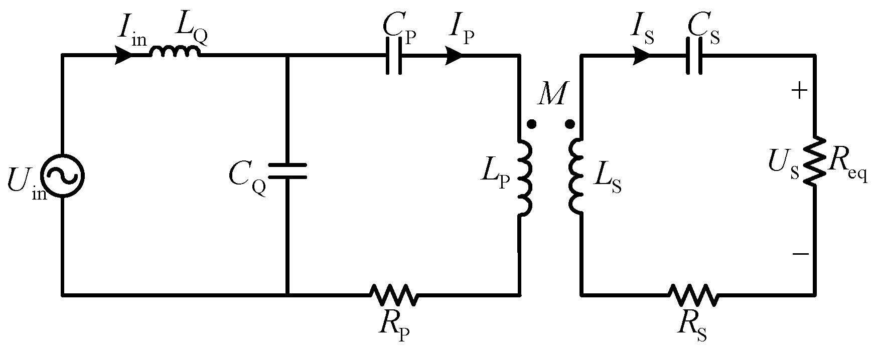
The block diagram of the LCC-S type WPT system is shown in Figure 1. This system consists of a DC input voltage source U, a full-bridge inverter, an LCC-S type compensation network, a rectifier bridge, and a load RL. The LCC-S compensation network comprises primary-side compensation inductors LQ, compensation capacitors CQ and CP, and secondary-side compensation capacitor CS. LP and LS represent the self-inductance of the transmitter coil and receiver coil, respectively. RP and RS denote the internal resistance of the transmitter coil and receiver coil, respectively. M is the mutual inductance between the coils.
According to the fundamental wave analysis method, the equivalent mutual inductance model of the LCC-S type WPT system is illustrated in Figure 2. In the figure, Uin and Iin represent the output voltage and output current of the inverter, respectively; IP and IS denote the currents of the transmitter-side coil and receiver-side coil, respectively; and Req is the equivalent resistance at the receiver end.
According to Kirchhoff’s voltage law, the loop formula is
U in = I in j ω L Q + ( I in I P ) j ω C Q U in = I in j ω L Q + I S j ω M + I P ( j ω L P + 1 j ω C P + R P ) I S R eq = I S ( j ω L S + 1 j ω C S + R S ) + I P j ω M
When the system is in a resonant state, the following relationship holds
1 ω C Q = ω L Q 1 ω C S = ω L S 1 ω C P = ω L P ω L Q
Combining Formulas (1) and (2), the output current Iin of the inverter, the transmitter-side coil current IP, and the receiver-side coil current IS are given by
I in = U in ω 2 M 2 + R P ( R eq + R S ) ω 2 L Q 2 ( R eq + R S ) I P = U in j ω L Q I S = U in M L Q ( R eq + R S )
The input power Pin and output power Pout of the system are
P in       = U in I in = U in 2 ω 2 M 2 + R P ( R eq + R S ) ω 2 L Q 2 ( R eq + R S ) P out = I S 2 R eq = U in 2 M 2 R eq L Q 2 ( R eq + R S ) 2
The efficiency of the fundamental wave output from the inverter to the load is then obtained as
η L = P out P in = ω 2 M 2 R eq ω 2 M 2 ( R S + R eq ) + R P ( R S + R eq ) 2
In the WPT system, the full-bridge inverter produces a square wave voltage with relatively high harmonic content. Additionally, energy passing through the compensation network experiences power losses, which reduce system efficiency. Therefore, increasing the fundamental component ratio in the inverter’s output voltage is an effective method to enhance the overall transmission efficiency of the WPT system.

3. Design of a Novel Seven-Level Inverter

To increase the fundamental wave content ratio in the inverter output waveform and reduce topological complexity, this can be achieved by optimizing the switch conduction angle and appropriately selecting the number of levels.

3.1. Optimization of Switch Conduction Angle and Selection of Optimal Number of Levels for Inverter

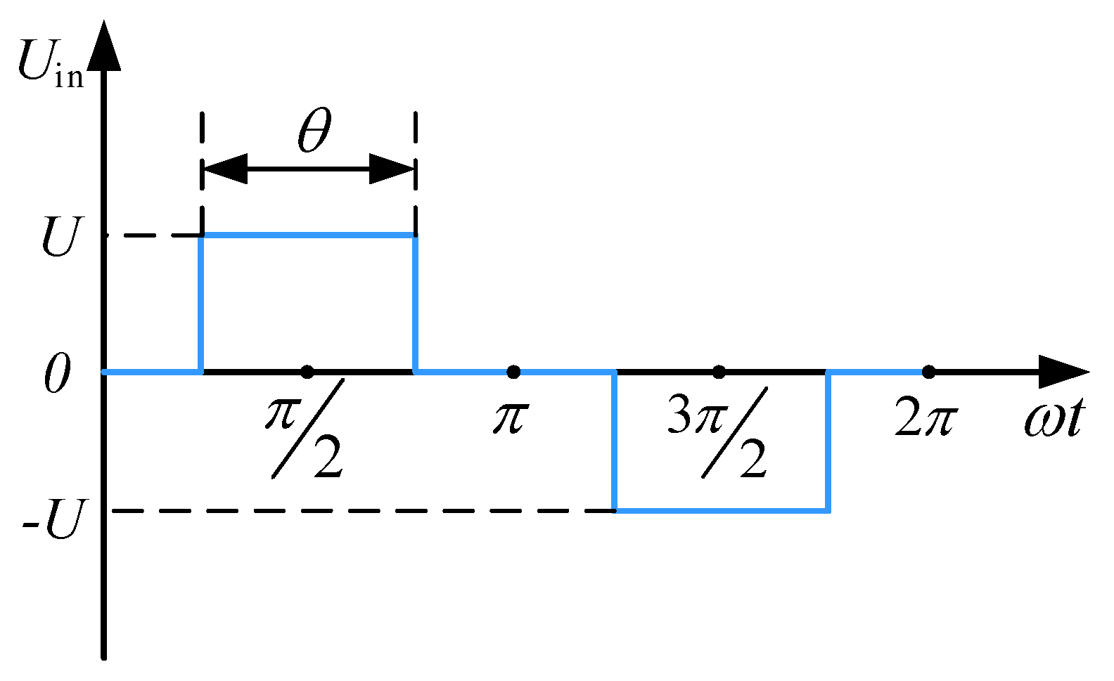
Taking the output voltage of a three-level inverter as an example for analysis, its schematic diagram is shown in Figure 3.
If the DC input voltage to the inverter is U, its output voltage can be expressed as
U in =           U , ω t π 2 θ 2 , π 2 + θ 2 U , ω t 3 π 2 θ 2 , 3 π 2 + θ 2         0 ,   others
where θ represents the conduction angle of the switch, where θ ∈ [0, 2π].
According to Fourier decomposition, the output voltage expression is
U in = 4 U π k = 1 , 3 , 5 1 k 1 2 sin ( k 2 θ ) k sin ( k ω t )
The effective value of its fundamental component is
U 1 m = 2 2 U π sin θ 2
Since the total width of the interval where Uin takes values of ±U within one cycle is 2θ, the effective value of the inverter output voltage is
U in ( m ) = 2 T 0 T 2 U ( t ) 2 d t = U θ π
The fundamental wave content ratio is
η = U 1 m U in ( m ) = 2 2 π θ sin θ 2
Through iterative calculation, it is determined that the maximum fundamental wave content ratio of the system is ηmax = 96.06% when the conduction angle θ = 133.6°.
By extending the inverter level structure through the principle of phase superposition, when the number of output voltage levels is m = 2n + 1, the effective value of the fundamental component of the output voltage is
U 1 m =       2 2 U π             , level   number   is   2 2 2 U π i = 1 n sin θ i 2 , level   number   is   2 n + 1
The effective value of the inverter output voltage is
U in ( m ) =       U           , level   number   is   2 U i = 1 n ( 2 i 1 ) θ i π , level   number   is   2 n + 1
The fundamental component ratio of the output voltage is
η i =     2 2 π             , level   number   is   2 2 2 i = 1 n sin θ i 2 π × i = 1 n ( 2 i 1 ) θ i , level   number   is   2 n + 1
By deriving from Formula (13), the optimal conduction angles and the fundamental wave content ratio of the inverter under different level numbers are obtained. Taking level numbers 2, 3, 5, 7, and 9 as examples, the results are shown in Table 1.
As shown in Table 1, the fundamental wave content proportion of multilevel inverters increases with the number of levels. When the multilevel inverter outputs seven levels or more levels, the fundamental wave content proportion approaches saturation. Furthermore, as the number of levels increases, the inverter topology becomes more complex. Therefore, this paper sets the multilevel count to seven levels.

3.2. Structure and Advantages of a Novel Seven-Level Inverter

Compared to conventional multilevel inverters, the switched-capacitor multilevel inverter structure features lower voltage stress on switches, reduced number of required switches, simpler modulation methods, balanced capacitor voltages, and high voltage gain.
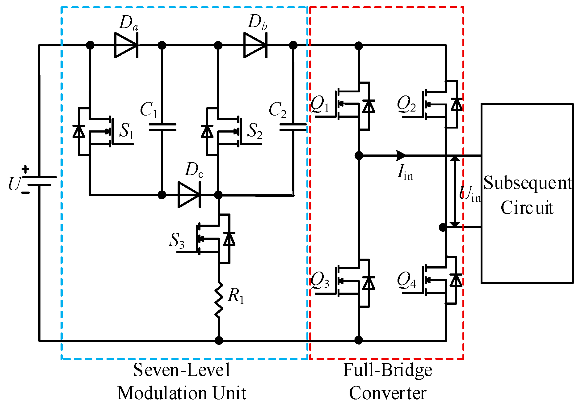
Based on the fundamental building blocks of switched-capacitor multilevel inverters, this paper proposes a novel seven-level inverter topology as shown in Figure 4. In Figure 4, resistor R1 serves to limit the high surge charging current of capacitors C1 and C2, whose rated voltage is U.
To validate the advantages of the proposed topology, a similar topology was selected for comparison, as shown in Table 2, the topology proposed in [10] does not require diodes and has a similar number of switches to the present work, but it exhibits the highest total stress per unit voltage for the switches. The topology proposed in [11] has a similar total stress per unit voltage for the switches as the present work, but it requires two external power supplies, the highest number of switching capacitors, and only one voltage gain. The topology proposed in [12] uses fewer diodes but has the highest number of switches, while also exhibits relatively high total stress per unit voltage for its switches. Therefore, the topology proposed in this paper offers advantages in reducing both the total stress per unit voltage of the switches and the number of switches required.

3.3. Modulation Method for Seven-Level Inverter

By controlling the turn-on timing of each switch, combined with capacitor charging/discharging and diode freewheeling, the seven-level inverter can achieve outputs at different voltage levels.
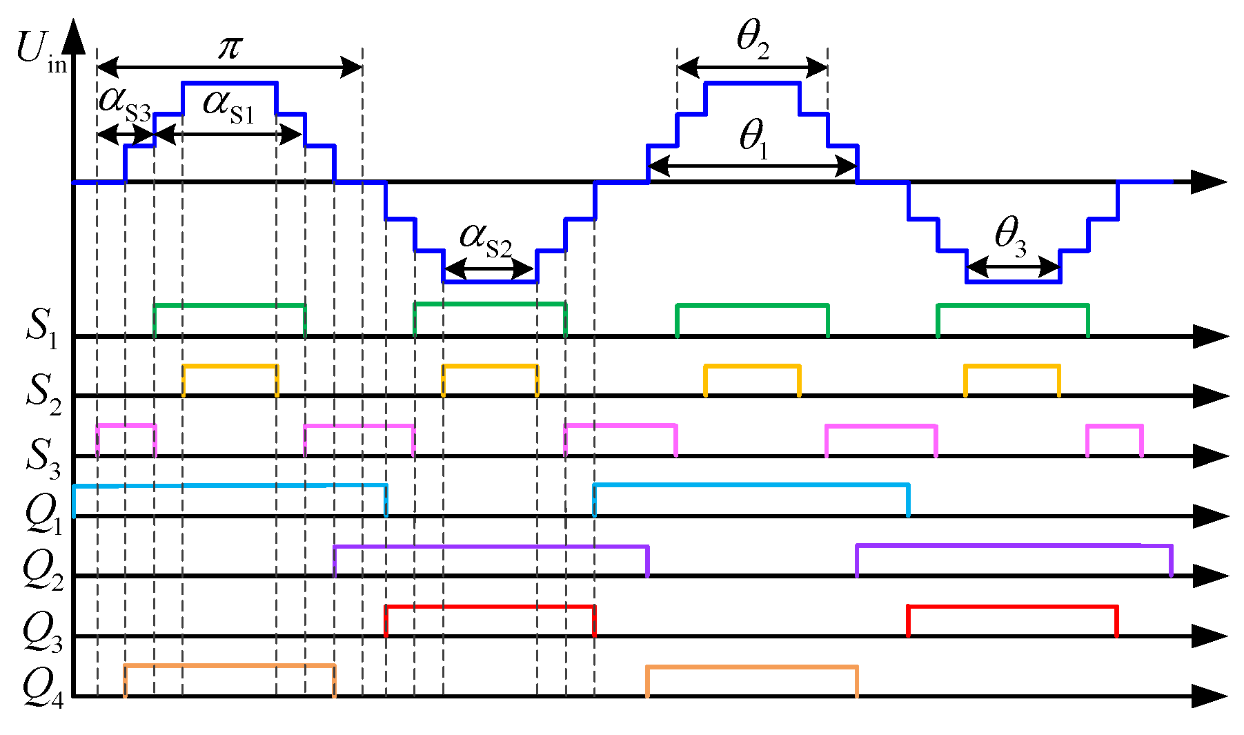
Using the seven-level optimal turn-on angle derived in Table 1, the turn-on timing diagram for the switch is obtained, as shown in Figure 5. Calculations indicate that the turn-on sequences for transistors S1S3 are αS1 = 124.2°, αS2 = 79.2° and αS3 = 27.9°, respectively.
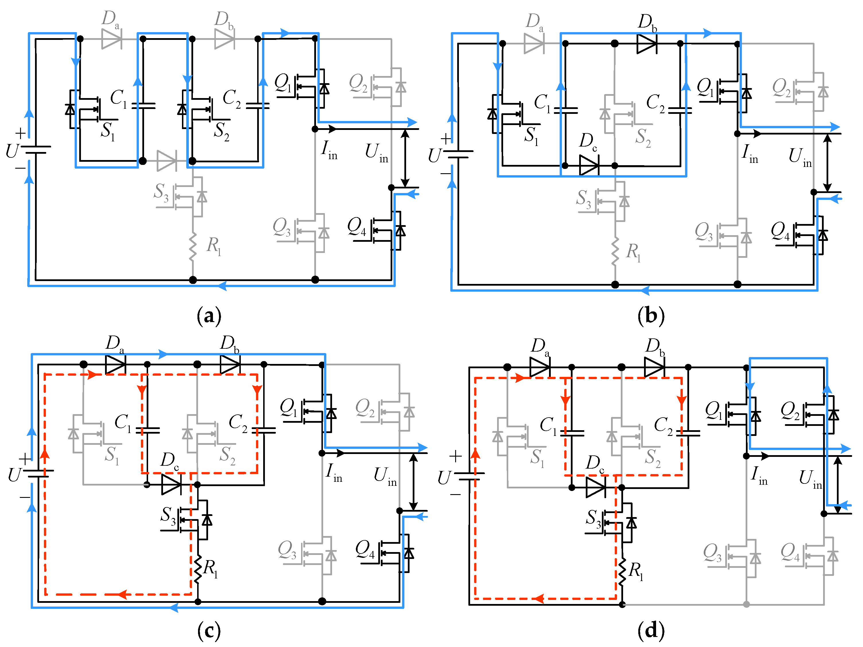
Based on the switching combinations of the power switches, Table 3 shows the output voltage, switch states, and capacitor states of the seven-level inverter during one cycle. Figure 6 illustrates the operating mode of the seven-level inverter during the positive half-cycle.
Mode I: In Figure 6a, switches Q1 and Q4 are turned on, and capacitors C1 and C2 discharge in series, providing voltage together with the power supply U. At this time, the seven-level inverter output a voltage level of 3U.
Mode II: In Figure 6b, switches Q1 and Q4 are turned on, and capacitors C1 and C2 discharge in parallel, providing voltage together with the power supply U. At this time, the seven-level inverter output a voltage level of 2U.
Mode III: In Figure 6c, switches Q1 and Q4 are turned on, and capacitors C1 and C2 continue charging. The power supply U provides the voltage, and the seven-level inverter output a voltage level of U.
Mode IV: In Figure 6d, switches Q1 and Q2 are turned on, and capacitors C1 and C2 begin charging. At this time, the seven-level inverter output a zero voltage level.
Similarly, by controlling the switches Q2 and Q3 along with S1S3, the seven-level inverter can generate a three-level trapezoidal wave output during the negative half-cycle.
The novel seven-level inverter topology proposed in this paper requires fewer switching state transitions during level switching compared to traditional multilevel inverter topologies, thereby helping to reduce switching losses. Furthermore, through capacitor charging and discharging, this topology can achieve up to three times the voltage gain.
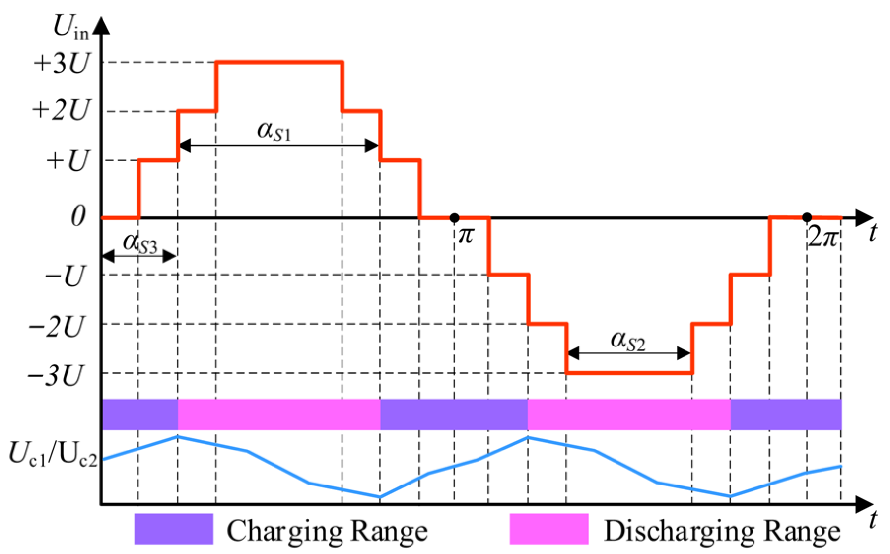
Within a modulation cycle, the capacitor operating states are illustrated in Figure 7, with the continuous discharge intervals for capacitors C1 and C2 are [αS3, π − αS3] and [π + αS3, 2π − αS3], respectively.
To suppress voltage ripple, an appropriate capacitance value must be selected. The inverter’s output current iin can be simplified as
i in = I m sin ( ω t + φ )
where Im represents the output current magnitude, ω denotes the angular frequency of the output voltage, and φ is the impedance angle.
Since the seven-level inverter WPT system operates at high frequencies, it is assumed that the output current remains constant over one cycle. Therefore, the currents ic1 and ic2 through capacitors C1 and C2 can be expressed as
i c 1 = i c 2 = i in = I m sin ( ω t + φ )
When capacitors C1 and C2 are in parallel, the discharge capacity is
Q 1 = 1 2 α S 3 π α S 2 2 i in d ω t
where ΔQ1 represents the respective discharge quantities of capacitors C1 and C2.
When capacitors C1 and C2 are in series, the discharge capacity is
Q 2 = π α S 2 2 π + α S 2 2 i in d ω t
where ΔQ2 represents the respective discharge quantities of capacitors C1 and C2.
Within half a cycle, the total discharge of capacitors C1 and C2 is
Q T = 2 × Q 1 + Q 2
The optimal capacitance value is expressed as
C opt Q T / β V ci
where β represents the percentage of ripple voltage, and Vci denotes the rated voltage of capacitors C1 and C2.
In summary, the fundamental efficiency of a seven-level inverter can be expressed as
η m = P m P s = 1 T 0 T u m i m d t 1 T 0 T u in i in d t
where Pm and Ps represent the fundamental power and input power of the seven-level inverter, respectively, while um and im denote the fundamental output voltage and current. Since the system operates at high frequencies, it can be assumed that im = iin. Therefore, the efficiency of the seven-level inverter can be expressed using the fundamental power fraction.
When the inverter outputs a seven-level trapezoidal wave, combining Formulas (5) and (13) yields the efficiency η7 of the WPT system from the DC power supply input to the load is
η 7 = η L η 3 = ω 2 M 2 R eq ω 2 M 2 ( R eq + R S ) + R P ( R eq + R S ) 2 × 2 2 ( sin θ 1 2 + sin θ 2 2 + sin θ 3 2 ) π ( θ 1 + 3 θ 2 + 5 θ 3 )
where η3 represents the fundamental wave content ratio of the seven-level inverter output.
When the inverter outputs a two-phase square wave, the efficiency η1 of the WPT system from the DC power source input to the load is
η 1 = η L η 0 = 2 2 ω 2 M 2 R eq π ω 2 M 2 ( R S + R eq ) + R P ( R S + R eq ) 2
where η0 represents the proportion of fundamental wave content in the two-level output.
Comparing Formulas (21) and (22), the overall transmission efficiency ratio of the WPT system is
η 7 η 1 > 1
The above formula demonstrates that the novel seven-level inverter proposed in this paper exhibits significantly higher efficiency than that of a full-bridge inverter.

4. Maximum Efficiency Tracking Based on Current Amplitude Ratio with Closed-Loop PI Control

When the coupling coefficient or load changes deviate from the maximum efficiency point, the efficiency of the WPT system significantly decreases. To address this, this paper employs a closed-loop PI control strategy based on the current amplitude ratio to ensure maximum efficiency tracking when the system deviates from the maximum efficiency point.

4.1. Maximum Efficiency Based on Current Amplitude Ratio

To further enhance the efficiency of the WPT system, the transmission efficiency η7 must be increased to its theoretical maximum value, defined as
η 7 R eq = 0 2 η 7 R eq 2 < 0
From Formulas (21) and (24), the optimal equivalent load value for the system at maximum transmission efficiency can be determined as
R eq . opt = R S 2 + ω 2 k 2 L P L S R S R P
From Formula (25), it is evident that when the system operates at the point of maximum transfer efficiency, Req.opt is positively correlated with k. However, obtaining the value of k in real time requires simultaneous measurement of primary and secondary side voltages and currents, increasing sampling complexity. Therefore, this paper employs a closed-loop PI controller based on the current amplitude ratio to achieve maximum efficiency tracking.
Define the ratio of the amplitude of the receiving coil current IS to the transmitting coil current IP as ρ. When the WPT system operates in a resonant state, Formula (3) expresses ρ as
ρ = I S I P = ω M R eq + R S
Combining Formulas (21) and (26) yields the relationship between the efficiency η7 and the current amplitude ratio ρ:
η 7 = 2 2 ( ω M ρ R S ρ 2 ) ( sin θ 1 2 + sin θ 2 2 + sin θ 3 2 ) ( ω M ρ + R P ) π ( θ 1 + 3 θ 2 + 5 θ 3 )
In high-frequency wireless power transfer systems, since R S / ω M 1 , combining Formulas (25) and (26) yields the optimal current amplitude ratio ρopt as
ρ opt R P / R S
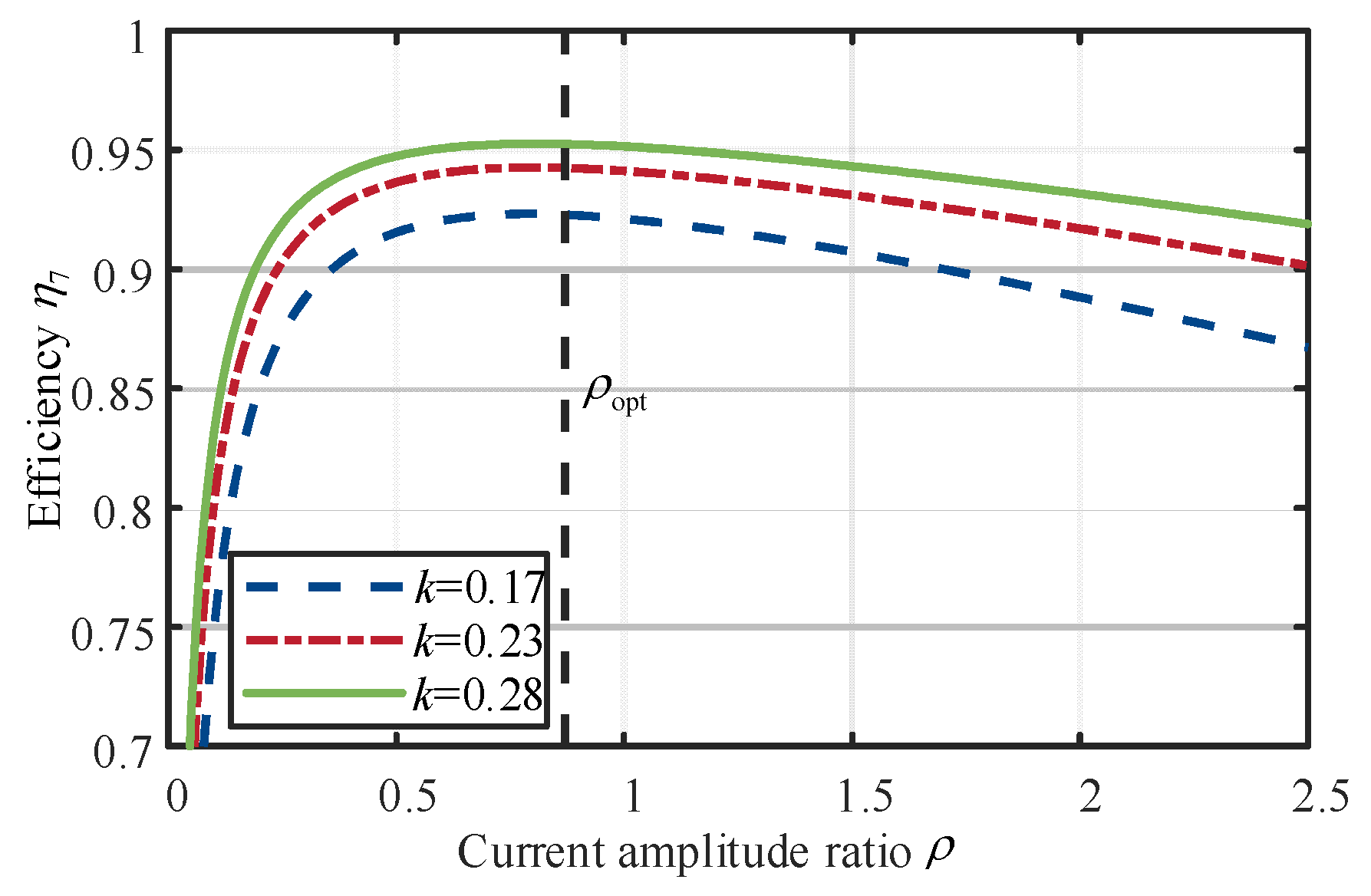
According to Formula (27), the relationship between efficiency η7 and current amplitude ratio ρ for different k values is shown in Figure 8.
As shown in Figure 8, the system exhibits a maximum efficiency point at different values of k, and it can reach the maximum efficiency point when ρ is close to ρopt. Formula (28) indicates that ρopt is independent of k. Since only the current amplitude needs to be detected without requiring phase information, this method simplifies the current sampling circuit while achieving maximum efficiency tracking.

4.2. Design of Closed-Loop PI Control Structure Based on Maximum Efficiency Tracking

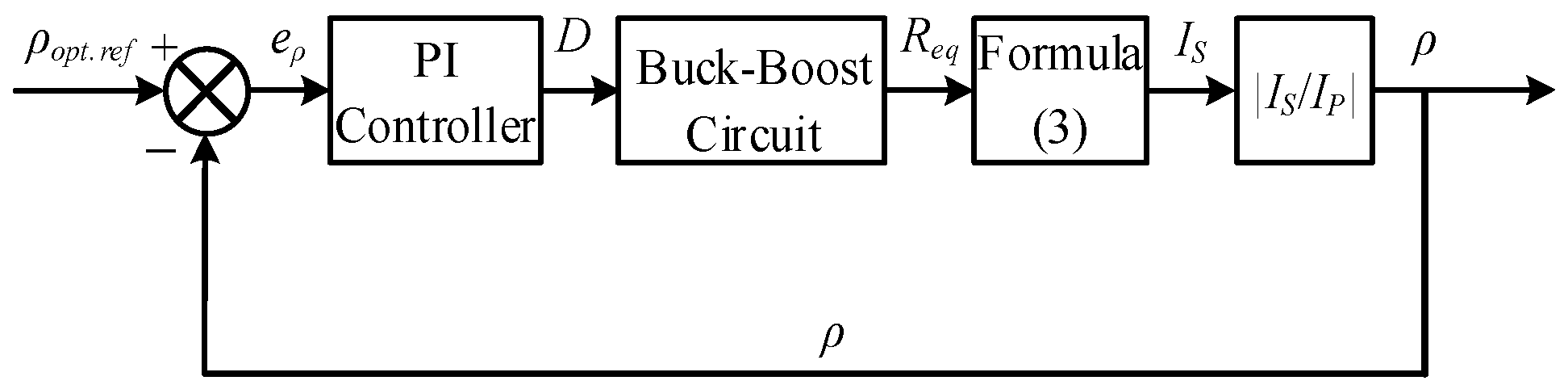
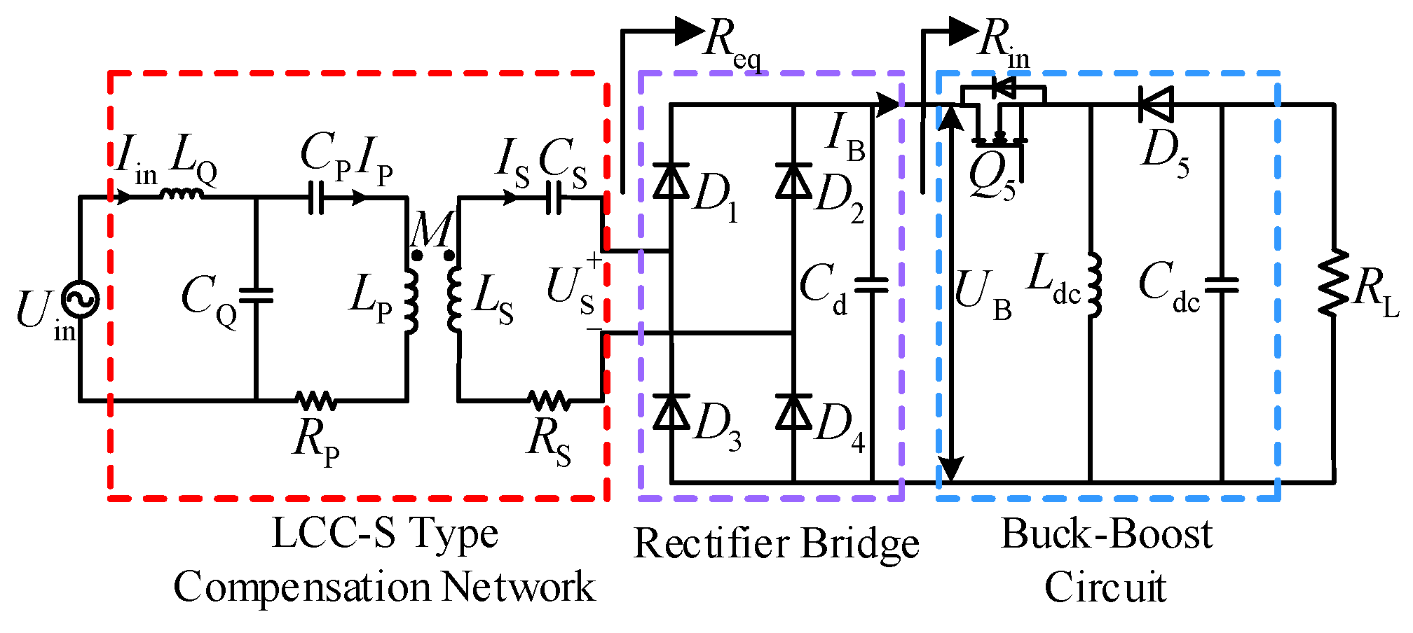
Based on Formulas (3) and (29), when the other parameters are known, the current IS in the receiving coil can be modified by adjusting the equivalent resistance Req, thereby indirectly regulating the parameter ρ. To enable continuous adjustment of Req over a wide range, the system employs a buck-boost circuit. After its integration, the relationship between the equivalent resistance Req at the WPT receiving end and the load resistance RL is as follows:
R eq = 8 R L π 2 ( 1 D D ) 2
Combining Formulas (26) and (29) yields the current amplitude ratio ρ:
ρ = ω M 8 R L π 2 ( 1 D D ) 2 + R S
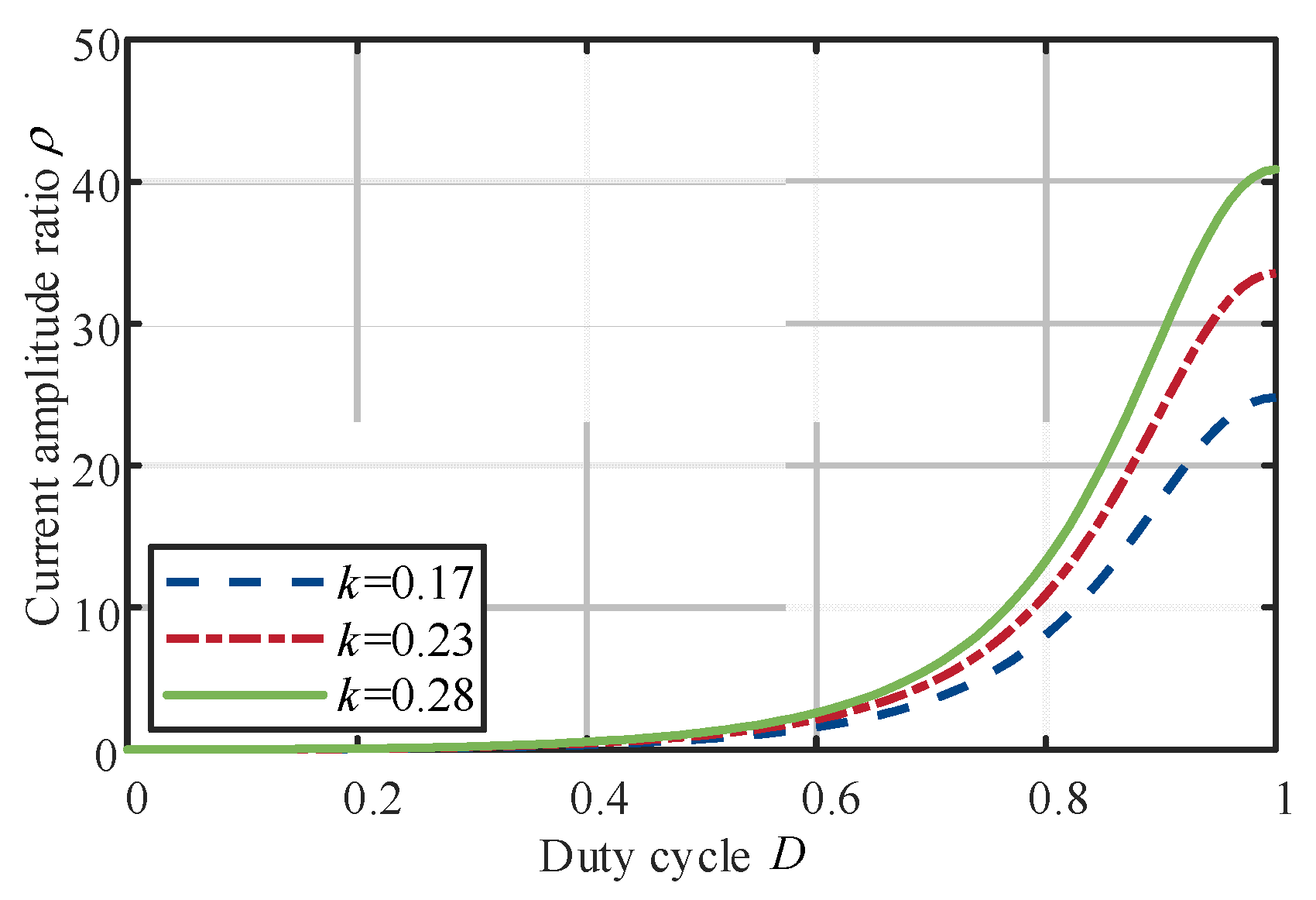
According to Formula (30), the relationship between the current amplitude ratio ρ and the duty cycle D for different k values is shown in Figure 9.
As shown in Figure 9, ρ increases monotonically with increasing D. Therefore, a PI controller can be employed to regulate, thereby adjusting ρ to ρopt.
The WPT system structure incorporating the buck-boost circuit is shown in Figure 10.
In summary, the current amplitude ratio PI control block diagram shown in Figure 11 can be obtained.

5. Experimental Verification

5.1. Experimental Setup

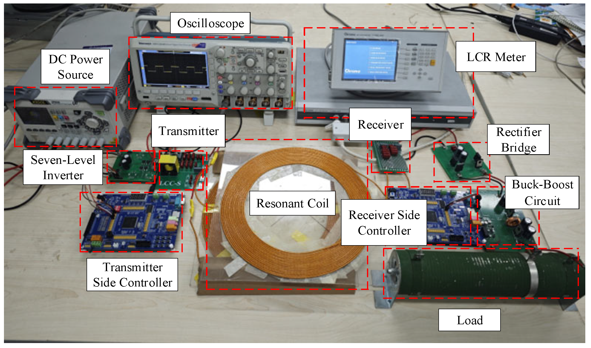
To validate the novel seven-level inverter structure and the effectiveness and correctness of the maximum efficiency tracking method proposed in this paper, an experimental setup was constructed as shown in Figure 12.
In Figure 12, a RIGOL DP832A is used to provide a DC power supply, a Chroma 11050−5M is used to measure the self-inductance of the coil, and a Tektronix MSO2024B oscilloscope is used to record the experimental waveforms.
The basic parameters of the experimental setup are shown in Table 4.

5.2. Experimental Results

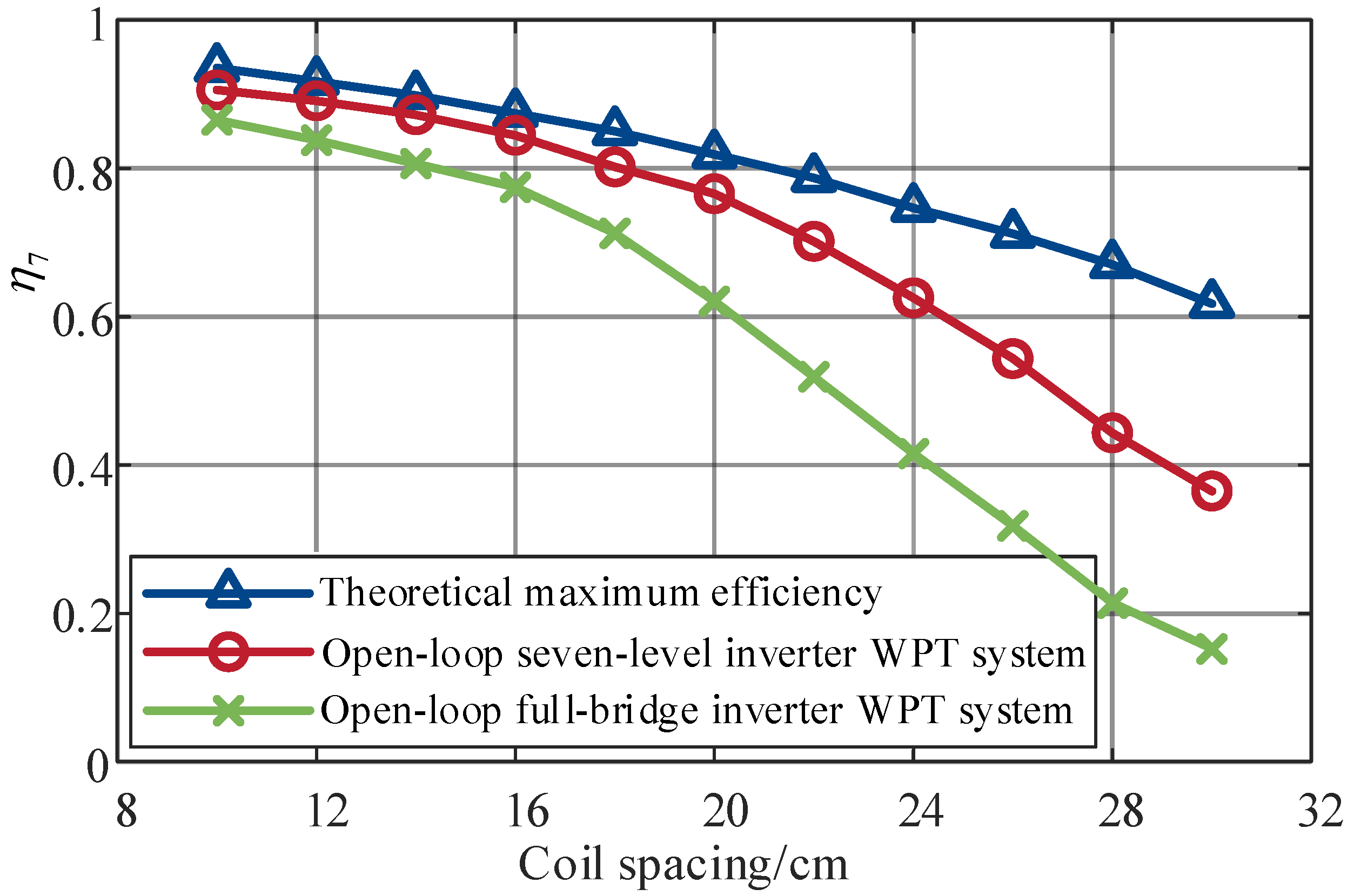
To verify that the transmission efficiency of the seven-level inverter WPT system outperforms that of the conventional inverter WPT system, the load resistance was set to 20 Ω under open-loop conditions. Experimental measurements of the transmission efficiency for both WPT systems at different coil spacings were obtained and compared with theoretical values. The resulting efficiency comparison curves for the two WPT systems are shown in Figure 13.
As shown in Figure 13, compared to the conventional inverter WPT system, the novel seven-level inverter WPT system demonstrates significant efficiency advantages. When the coil spacing is within 12 cm (indicating a high coupling coefficient), its transmission efficiency approaches the theoretical maximum value. As the coil spacing varies, the overall transmission efficiency of the system increases by an average of 7.4%, showing an increasing trend with greater spacing.
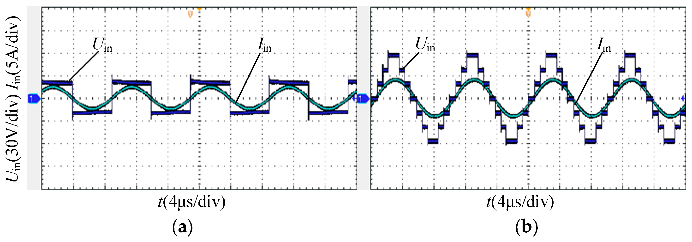
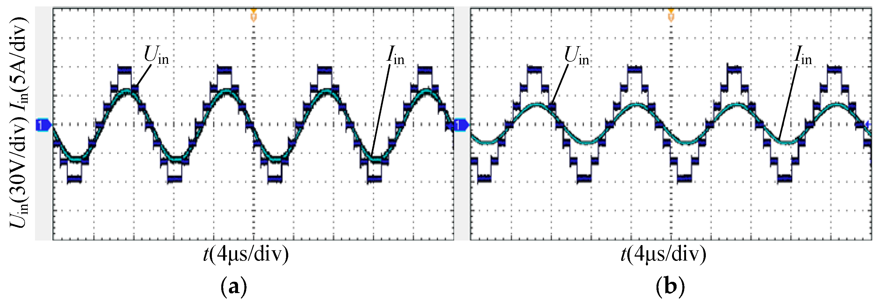
At this point, when only different inverters were used while all other experimental conditions remained consistent, the inverter output voltage and current waveforms for the two WPT systems are shown in Figure 14a,b. Compared to the full-bridge inverter WPT system, the new seven-level inverter WPT system produces an output voltage that more closely approximates a sine wave and a sinusoidal output current, thereby enabling more efficient operation of the WPT system.
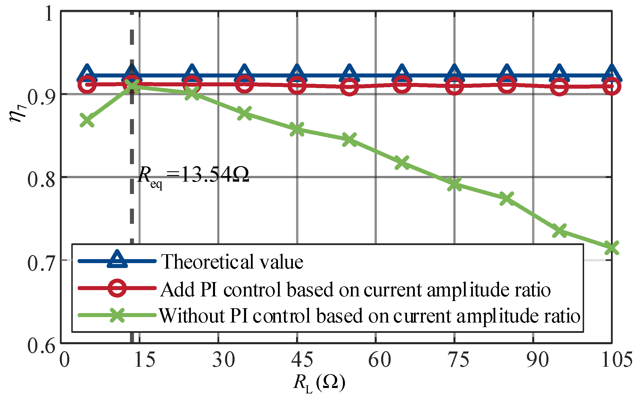
To verify whether the seven-level inverter WPT system can achieve maximum efficiency tracking under different load resistance values, experiments were conducted with a coil spacing of 12 cm and ρopt set to 0.9. The experimental results were used to plot the system transmission efficiency versus load relationship diagram shown in Figure 15.
As shown in Figure 15, when the WPT system operates without current-amplitude-ratio-based PI control, the transmission efficiency initially increases but then declines as the load RL continues to rise. Upon incorporating current-amplitude-ratio-based PI control, the system’s transmission efficiency fluctuates minimally and approaches the theoretical calculated value by adjusting the duty cycle of the Buck-Boost circuit. For RL values of 35 Ω, 55 Ω, and 75 Ω, respectively, the overall efficiency of the system with this control increased by 3.52%, 6.69%, and 9.46%, respectively, compared to the system without this control.
At this point, the output voltage and current waveforms of the seven-level inverter are shown in Figure 16a,b. According to Formula (3), when the system is in steady state under the maximum efficiency tracking control strategy, the resistance values of Req corresponding to different loads converge to the same level. Therefore, the magnitude of the inverter output current Iin remains essentially consistent, demonstrating the effectiveness of the maximum efficiency tracking control strategy under varying loads. When RL is 10 Ω and 30 Ω, the magnitudes of the inverter output current Iin are 5.2 A and 5.1 A, respectively.
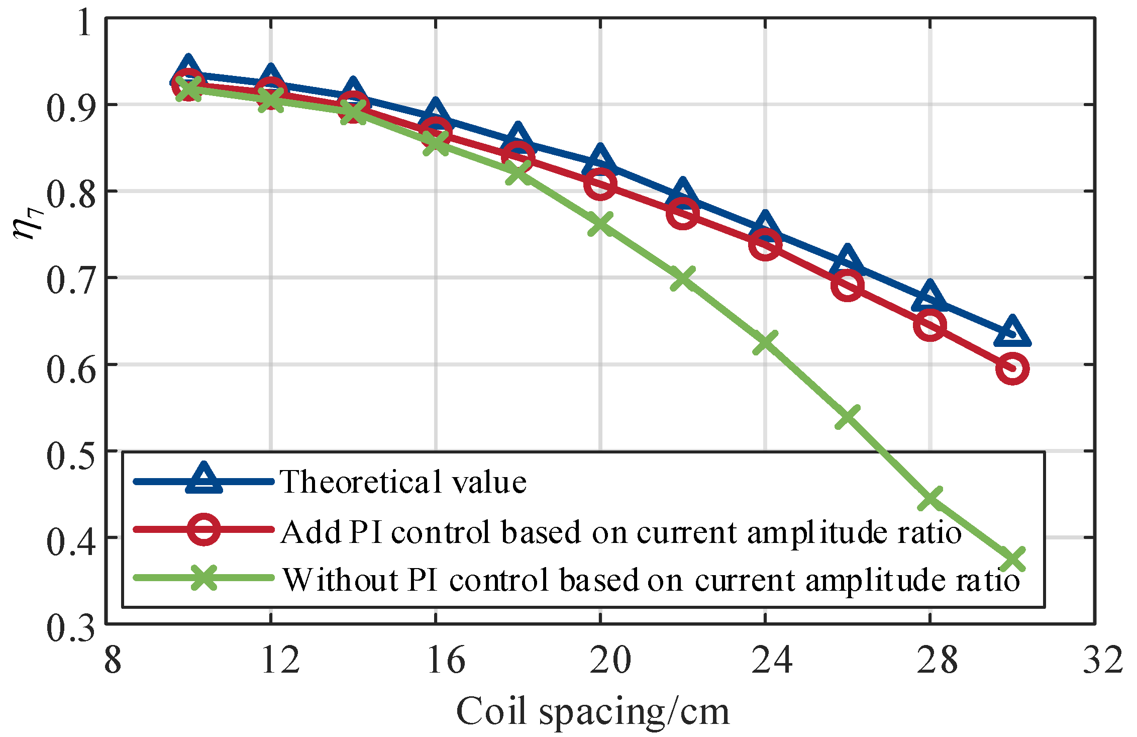
To verify whether the seven-level inverter WPT system can achieve maximum efficiency tracking at different coil spacings, experiments were conducted with RL set to 15 Ω and ρopt set to 0.9. The experimental results were used to plot the relationship between system transmission efficiency and coil spacing, as shown in Figure 17.
As shown in Figure 17, when the WPT system lacks current-amplitude-ratio-based PI control, the transmission efficiency noticeably declines as the coil spacing increases, gradually deviating from the theoretical calculation values. When this control is incorporated, the transmission efficiency still decreases but remains close to the theoretical calculation value. At coil spacings of 16 cm, 20 cm, and 24 cm, the overall efficiency of the system with this control increased by 1.2%, 4.6%, and 11.3%, respectively, compared to the system without this control.
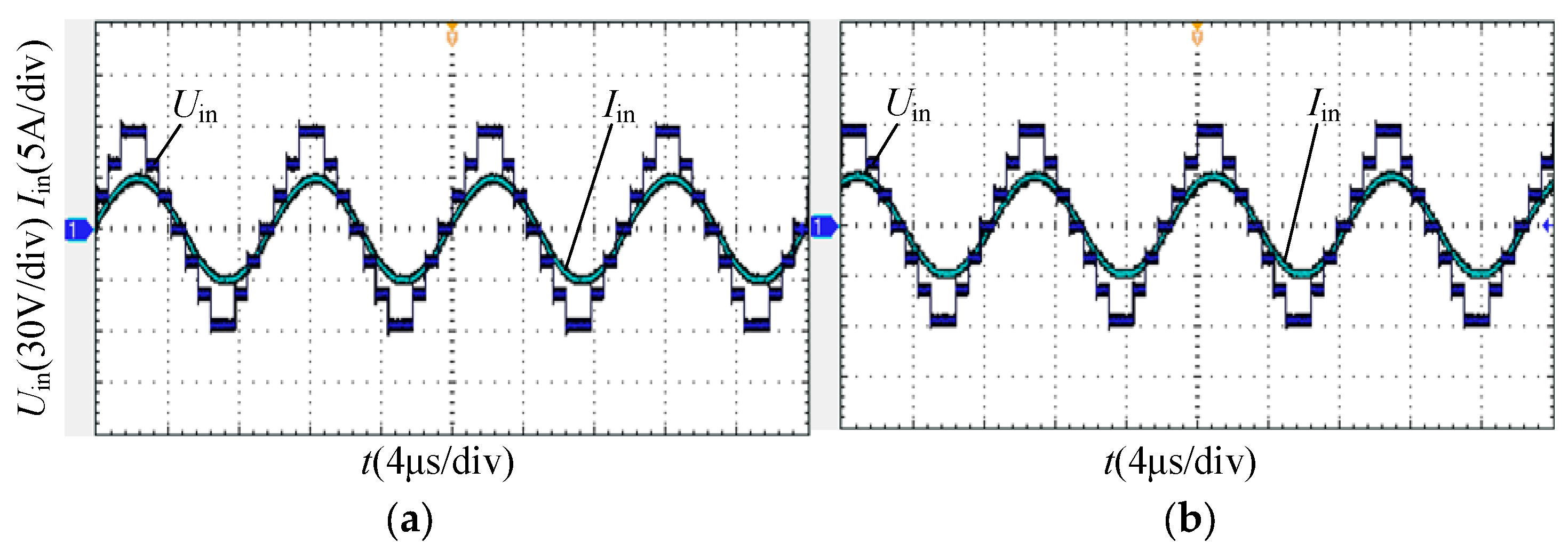
At this point, the inverter output voltage and current waveforms are shown in Figure 18a,b. According to Formula (3), when RL is the same, the inverter output current Iin is only positively correlated with k, resulting in different magnitudes of the inverter output current Iin. When the coil spacing is 10 cm and 16 cm, respectively, the magnitudes of the inverter output current Iin are 6.6 A and 3.4 A.
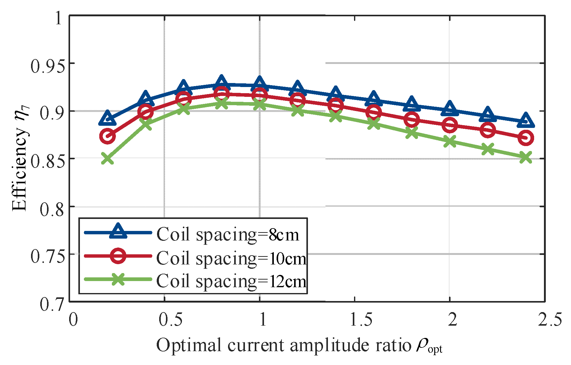
To verify the impact of ρopt values on the system’s maximum efficiency tracking, three sets of different coil spacings were set for comparison. When RL is 15 Ω, the relationship between system transmission efficiency and the optimal current amplitude ratio was plotted as shown in Figure 19.
As shown in Figure 19, the transmission efficiency of the system under three different coil spacing configurations exhibits a trend of first increasing and then decreasing as the value of ρopt increases. In all cases, the maximum efficiency point is achieved near ρopt = 0.9, thereby enabling optimal efficiency tracking for the system.
As shown in Figure 15 and Figure 17, when the system was tested under varying load and coil spacing conditions, the deviation between the efficiency tracked by the algorithm and the theoretical maximum efficiency was approximately 3%. This deviation primarily stems from losses inherent to the switches and coils themselves. It also demonstrates that the proposed method can effectively approximate the theoretical optimum value.
The comparison results between the maximum efficiency tracking method proposed in this paper and existing literature methods are shown in Table 5.

6. Conclusions

This paper proposes a novel seven-level inverter topology for wireless power transfer (WPT) systems. By employing a maximum efficiency tracking strategy based on current amplitude ratio closed-loop PI control, it achieves maximum efficiency tracking under varying coupling coefficient and load. First, by comparing the conduction angle of the inverter’s switches and the fundamental wave content ratio across different levels, a seven-level inverter is selected to enhance overall system efficiency. Second, the relationship between current amplitude ratio and system transmission efficiency is derived. Analysis indicates that system transmission efficiency peaks at the optimal current amplitude ratio, which depends solely on coil resistance and is independent of the coupling coefficient. Finally, a buck-boost circuit is introduced at the receiver side, employing closed-loop PI control based on current amplitude ratio to dynamically regulate this ratio. Experiments demonstrate that system efficiency remains stable at approximately 91.4% during load variations. When coil spacing changes (i.e., coupling coefficient variations), system efficiency approaches theoretical calculations, achieving maximum efficiency tracking.

Author Contributions

Methodology, W.H. and W.Y.; Validation, W.Y. and H.T.; Formal analysis, Y.C.; Data curation, H.T.; Writing—original draft preparation, W.Y. All authors have read and agreed to the published version of the manuscript.

Funding

This research was funded by the National Natural Science Foundation of China, grant number 62473133.

Data Availability Statement

Data is contained within the article.

Conflicts of Interest

The authors declare no conflicts of interest.

References

  1. Liao, Z.J.; Zhu, Q.W.; Ren, W.; Xia, C.Y.; Liu, X. Energy efficiency characteristic analysis of tri-coil PT symmetric MC-WPT systems. J. Power Electron. 2023, 23, 1285–1297. [Google Scholar] [CrossRef]
  2. Luo, J.; Shen, H.; Xu, X. DSP-based adaptive digital control method for frequency tracking and impedance angle control of MCR–WPT systems. J. Power Electron. 2025, 25, 555–564. [Google Scholar] [CrossRef]
  3. Liu, X.; Gao, F.; Wang, T.F.; Khan, M.M.; Zhang, Y.; Xia, Y. A multi-inverter multi-rectifier wireless power transfer system for charging stations with power loss optimized control. IEEE Trans. Power Electron. 2023, 38, 9261–9277. [Google Scholar] [CrossRef]
  4. Huang, W.C.; Rao, T.B.; Jiang, X.Y.; Hu, Y.; Chang, Y.F. Maximum efficiency tracking and constant voltage output compound control method for wireless power transfer system. Trans. Chin. Electrotech. Soc. 2024, 39, 3589–3601. [Google Scholar]
  5. Yenil, V.; Cetin, S. Load independent constant current and constant voltage control of LCC-series compensated wireless EV charger. IEEE Trans. Power Electron. 2022, 37, 8701–8712. [Google Scholar] [CrossRef]
  6. Xia, C.Y.; Li, X.L.; Han, X.Z.; Yang, X.H.; Li, X.Y.; Liao, Z.J. A hybrid control method for achieving constant voltage output with LADRC and maximum efficiency tracking for IPT systems. Proc. CSEE 2022, 42, 6042–6052. [Google Scholar]
  7. He, L.Z.; Guo, D. A clamped and harmonic injected class-E converter with ZVS and reduced voltage stress over wide range of distance in WPT System. IEEE Trans. Power Electron. 2021, 36, 6339–6350. [Google Scholar] [CrossRef]
  8. Huang, X.S.; Yu, Z.K.; Lin, S.Y.; Ouyang, Z.W.; Andersen, M.A.E. Load-independent push–pull class E2 topology with coupled inductors for MHz-WPT applications. IEEE Trans. Power Electron. 2022, 37, 8726–8737. [Google Scholar] [CrossRef]
  9. Guo, J.; Chau, K.T.; Liu, W.; Hou, Y.H.; Chan, W.L. Pulse magnitude modulation and token rotation-based voltage balancing method of multilevel inverter for wireless power transfer. IEEE Trans. Power Electron. 2025, 40, 4652–4663. [Google Scholar] [CrossRef]
  10. Ren, L.; Zhang, L.; Wang, L.; Dai, S.J. Capacitor voltage regulation strategy for 7-level single DC source hybrid cascaded inverter. IEEE J. Emerg. Sel. Top. Power Electron. 2022, 10, 5773–5784. [Google Scholar] [CrossRef]
  11. Manoj, P.; Kirubakaran, A.; Somasekhar, V.T. An asymmetrical dual quasi-z-source based 7-level inverter for PV applications. IEEE Trans. Energy Convers. 2023, 38, 1097–1107. [Google Scholar] [CrossRef]
  12. Jakhar, A.; Sandeep, N.; Verma, A.K. Common-ground-type inverter topology with low voltage stress and boosting ability. IEEE Trans. Circuits Syst. II Express Briefs 2024, 71, 2854–2858. [Google Scholar] [CrossRef]
  13. Lu, S.Y.; Bottigheimer, M.; Parapour, N. An impedance mapping-based T-compensation network and control strategy for WPT system with full-bridge active rectifier. IEEE Trans. Power Electron. 2023, 38, 14675–14688. [Google Scholar] [CrossRef]
  14. Zhao, Y.M.; Wang, Z.H.; Su, Y.G.; Qing, X.D.; Wu, X.Y. Load adaptive technology of constant voltage electric-field coupled power transfer system based on T-CLC resonant network. Trans. Chin. Electrotech. Soc. 2020, 35, 106–114. [Google Scholar]
  15. Li, Z.; Yu, Z.H.; Gao, S.H.; Tang, M.L.; Sun, H.X. Two-sided LCL zero voltage switching control strategy based on active rectifier for wireless power transfer system. Trans. Chin. Electrotech. Soc. 2025, 40, 2380–2392. [Google Scholar]
  16. Wu, Y.B.; Zhao, J.B.; Zhang, S.T.; Zhang, J.W.; Wang, X.L. An adaptive impedance matching method based on radial basis function neural network in multi-load wireless power transfer systems. Trans. Chin. Electrotech. Soc. 2021, 36, 3969–3977. [Google Scholar]
  17. Su, Y.G.; Yang, J.; Dai, X.; Liu, J.M.; Hou, X.Y. TensorFlow neural network based load and mutual inductance identification method for magnetic coupling resonant wireless power transfer system. Autom. Electr. Power Syst. 2021, 45, 162–169. [Google Scholar]
  18. Maile, P.; Jayalath, S. Parameter estimation using total harmonic distortion in a WPT system. IEEE Trans. Power Electron. 2025, 40, 57–63. [Google Scholar] [CrossRef]
  19. Liu, J.W.; Wang, G.B.; Xu, G.; Peng, J.C.; Jiang, H. A parameter identification approach with primary-side measurement for DC-DC wireless-power-transfer converters with different resonant tank topologies. IEEE Trans. Transp. Electrif. 2021, 7, 1219–1235. [Google Scholar] [CrossRef]
  20. Dai, R.M.; Zhou, W.; Chen, Y.H.; Zhu, Z.H.; Mai, R.K. Pulse density modulation based mutual inductance and load resistance identification method for wireless power transfer system. IEEE Trans. Power Electron. 2022, 37, 9933–9943. [Google Scholar] [CrossRef]
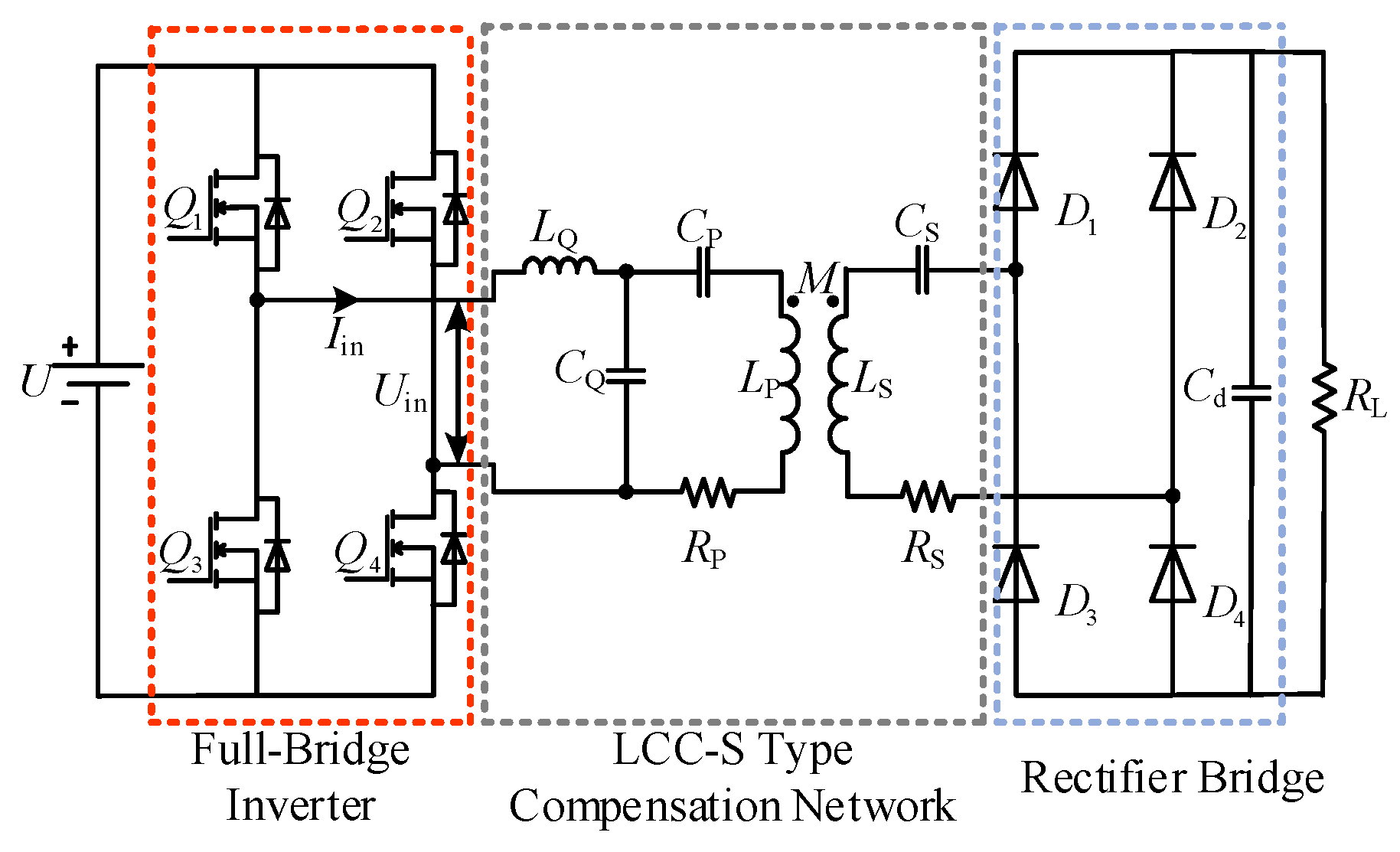
Figure 1. LCC-S type WPT system block diagram circuit.
Electronics 15 01433 g001
Figure 2. Equivalent mutual inductance model.
Electronics 15 01433 g002
Figure 3. Schematic diagram of three-level output voltage.
Electronics 15 01433 g003
Figure 4. Seven-level inverter structure.
Electronics 15 01433 g004
Figure 5. The turn-on timing diagram for the switch.
Electronics 15 01433 g005
Figure 6. The working mode of the level modulation unit when the output voltage Uin ≥ 0: (a) mode I; (b) mode II; (c) mode III; (d) mode IV; the blue line represents the working current path; the red line represents the charging current path.
Electronics 15 01433 g006
Figure 7. Capacitor operating state.
Electronics 15 01433 g007
Figure 8. Relationship curve diagram of efficiency η7 versus current amplitude ratio ρ at different k values.
Electronics 15 01433 g008
Figure 9. Relationship between current amplitude ratio ρ and duty cycle D for different k values.
Electronics 15 01433 g009
Figure 10. WPT system structure with buck-boost circuit.
Electronics 15 01433 g010
Figure 11. Current amplitude ratio PI control block diagram.
Electronics 15 01433 g011
Figure 12. WPT system experimental setup.
Electronics 15 01433 g012
Figure 13. Comparison chart of transmission efficiency between two WPT systems.
Electronics 15 01433 g013
Figure 14. Output voltage and current waveforms of different inverters with a coil spacing of 14 cm: (a) full-bridge inverter; (b) proposed inverter.
Electronics 15 01433 g014
Figure 15. Relationship diagram between system transmission efficiency and load.
Electronics 15 01433 g015
Figure 16. Output voltage and current waveforms of the seven-level inverter: (a) RL = 10 Ω; (b) RL = 30 Ω.
Electronics 15 01433 g016
Figure 17. Relationship diagram between system transmission efficiency and coil spacing.
Electronics 15 01433 g017
Figure 18. Output voltage and current waveforms of the seven-level inverter: (a) coil spacing is 10 cm; (b) coil spacing is 16 cm.
Electronics 15 01433 g018
Figure 19. Relationship diagram between system transmission efficiency and optimal current amplitude ratio.
Electronics 15 01433 g019
Table 1. Optimal conduction angles and fundamental wave percentages at different voltage levels.
Level
Number
θ1θ2θ3θ4Fundamental
Wave Proportion
2////90.01%
3133.6°///96.06%
5154.2°96.3°//98.68%
7162.0°124.2°79.2°/99.34%
9171.5°135.6°97.8°67.5°99.61%
Table 2. Comparative analysis of different inverter topologies.
ReferencesNLNDCNCNSWNDTSVpuK
[10]7128/12.03
[11]724825.661
[12]7121016.03
Proposed topology712735.333
NL number of levels; NDC number of DC sources; NC number of capacitors; NSW number of switches; ND number of diodes; TSVpu total standing voltage per-unit; K voltage gain.
Table 3. The output voltage, switch states, and capacitor status of the seven-level inverter.
Working ModeOutput LevelS1S2S3Q1Q2Q3Q4C1/C2
I3U1101001D
II2U1001001D
IIIU0011001C
IV00011100C
V00011100C
VIU0010110C
VII−2U1000110D
VIII−3U1100110D
‘1’ and ‘0’ represent the ‘on’ and ‘off’ states of the switches, respectively; ‘C’ and ‘D’ represent the ‘charging’ and ‘discharging’ states of the capacitors, respectively.
Table 4. Experimental setup parameters.
ParametersValues
Input voltage U20 V
Frequency f100 kHz
Self-inductance LP, LS142.26 μH, 142.16 μH
Compensation inductor LQ, Ldc22 μH, 200 μH
Compensation capacitor CQ, CP, CS115.14 nF, 21.06 nF, 17.82 nF
Coil resistance RP, RS0.4 Ω, 0.49 Ω
Storage capacitor C1, C2, Cdc680 μF, 680 μF, 100 μF
Table 5. Comparison with the existing literature methods.
ReferenceFundamental Proportion OptimizationCoupling Coefficient EstimationMaximum Efficiency TrackingEfficiency
This paperYesNo needYes91.4%
[6]NoNeedYes88%
[16]NoNeedYes89%
[17]NoNeedNo86.2%
Disclaimer/Publisher’s Note: The statements, opinions and data contained in all publications are solely those of the individual author(s) and contributor(s) and not of MDPI and/or the editor(s). MDPI and/or the editor(s) disclaim responsibility for any injury to people or property resulting from any ideas, methods, instructions or products referred to in the content.