

Article

A Preisach–MVS Compact-Modeling Framework for Investigating Device Variability in Ferroelectric FETs Under Ferroelectric Thickness and Coercive-Field Fluctuations

School of Physical Science and Technology, Lanzhou University, Lanzhou 730000, China
*
Authors to whom correspondence should be addressed.
Electronics 2026, 15(6), 1274; https://doi.org/10.3390/electronics15061274
Submission received: 28 January 2026 / Revised: 20 February 2026 / Accepted: 2 March 2026 / Published: 18 March 2026
(This article belongs to the Section Microelectronics)

Abstract

As emerging nonvolatile memory devices, ferroelectric field-effect transistors (FeFETs) have attracted significant attention for memory applications. However, due to the stochastic nature of fabrication processes and material properties, FeFETs exhibit pronounced device-to-device (DTD) variations, leading to threshold voltage dispersion and inconsistency in memory window (MW), which severely constrain array-level performance and reliability. In this study, a compact model-based variability analysis methodology for FeFETs has been proposed. Specifically, the Preisach ferroelectric (FE) hysteresis model was combined with the MIT Virtual Source (MVS) physical compact model to establish a macro-model for FeFETs, and statistical simulations were performed to evaluate device-level variations. Using the proposed framework, how fluctuations in two key FE parameters, film thickness (tFE) and coercive field (EC), affect FeFET transfer characteristics, threshold voltage (VTH), and MW was systematically investigated. Monte Carlo (MC) simulations were further conducted to quantify the distribution width and statistical features of VTH under different variability scenarios. The results indicate that random fluctuations in process-related parameters broaden the FeFET Id-Vg characteristics, induce shifts in high/low threshold voltages, and cause MW variations. Moreover, when tFE and EC fluctuate simultaneously, the dispersions of VTH and MW become significantly larger than those induced by a single-parameter fluctuation. The proposed compact-modeling framework and variability analysis approach enables the efficient evaluation of parameter tolerance and performance margin in FeFET arrays, providing guidance for storage-array design.

1. Introduction

As rapid advancements have been made in ferroelectric (FE) materials in microelectronics, emerging FE memories based on nanoscale thin films such as doped or alloyed HfO2 have attracted extensive attention [1,2,3,4,5]. In particular, ferroelectric field-effect transistors (FeFETs) exploit the switchable spontaneous polarization of an FE gate stack to achieve nonvolatile storage, offering key advantages including improved endurance, multilevel storage capability, and CMOS process compatibility [4,6,7,8]. Nevertheless, similar to conventional transistors, FeFETs are susceptible to stochastic process perturbations during fabrication, which can lead to pronounced device-to-device (DTD) variations in threshold voltage (VTH) [9,10,11,12]. More broadly, recent reviews focused on emerging thin-film device technologies have emphasized that scalable fabrication and device reproducibility under process tolerances are critical bottlenecks for practical deployment, rather than factors that merely contribute to achieving record performance [13,14]. This perspective directly motivates researchers to perform variability-aware FeFET modeling, where realistic process/material fluctuations in the ferroelectric gate stack must be translated into the statistical dispersions of key memory metrics such as VTH and MW. Early studies further indicate that the complex microstructure of polycrystalline FE films in the gate dielectric introduces additional randomness: the FE layer typically consists of grains with diverse sizes and orientations, local regions may reside in FE or non-FE phases, and grain-boundary vicinities are often accompanied by charge trapping and localized phase transitions. As a result, spatially nonuniform energy barriers and domain-structure fluctuations can emerge during polarization switching [15,16,17,18]. As the device footprint shrinks, the number of switchable ferroelectric (FE) domains (or grains) participating in switching is reduced, so the inherently stochastic nucleation and growth process translates into markedly larger DTD dispersions in both threshold voltage (VTH) and memory window (MW) [19]. This DTD variability has been repeatedly reported in experiments and TCAD studies, and is generally linked to the statistical nature of multi-domain switching in polycrystalline FE films, compounded by intrinsic microstructural and material inhomogeneity [20,21].
Despite the fact that meaningful progress has been made in terms of modeling randomness-induced variations in FeFET characteristics, most prior studies either (i) keep the FE layer thickness fixed and perturb only a limited subset of parameters, or (ii) approximate the FE as an effectively homogeneous dielectric and introduce variability predominantly at the interface and/or in the underlying channel stack. As a result, the scientific community still lacks a systematic understanding of how simultaneous fluctuations of multiple intrinsic FE parameters jointly shape both the static behavior and the statistical (distribution-level) characteristics of FeFETs. To address this research gap, our study provides a unified variability framework that co-considers coupled FE–parameter fluctuations and quantifies their combined impact on VTH and MW evolution under scaling, thereby offering clearer physical attribution and more actionable design guidance for variability-aware FeFET optimization. In particular, since our primary objective is to perform large-sample DTD statistical evaluation and sensitivity analysis with manageable computational cost, we concentrate on quasi-static Id-Vg characteristics and the resulting VTH and MW distributions, which are the most direct metrics for read/write margin assessment in FeFET arrays. Incorporating switching dynamics and reliability metrics, such as endurance and retention, would typically require additional time-dependent parameters and degradation models, and also rely on more extensive experimental calibration data. Therefore, this is absent from our study and should be the subject of future work.

2. Modeling Methodology

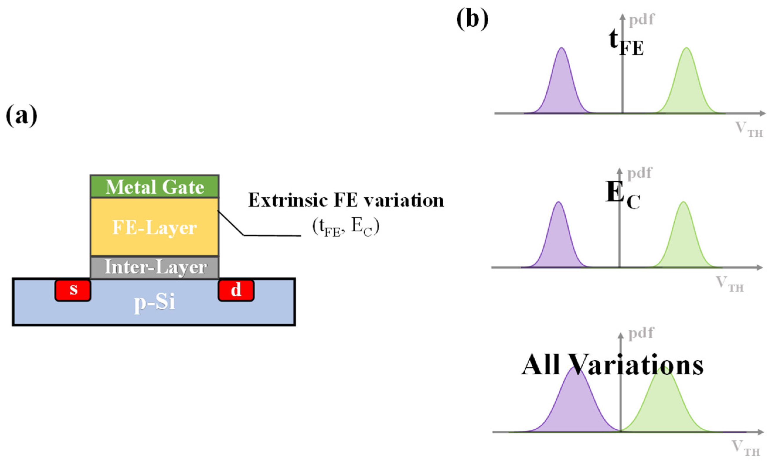
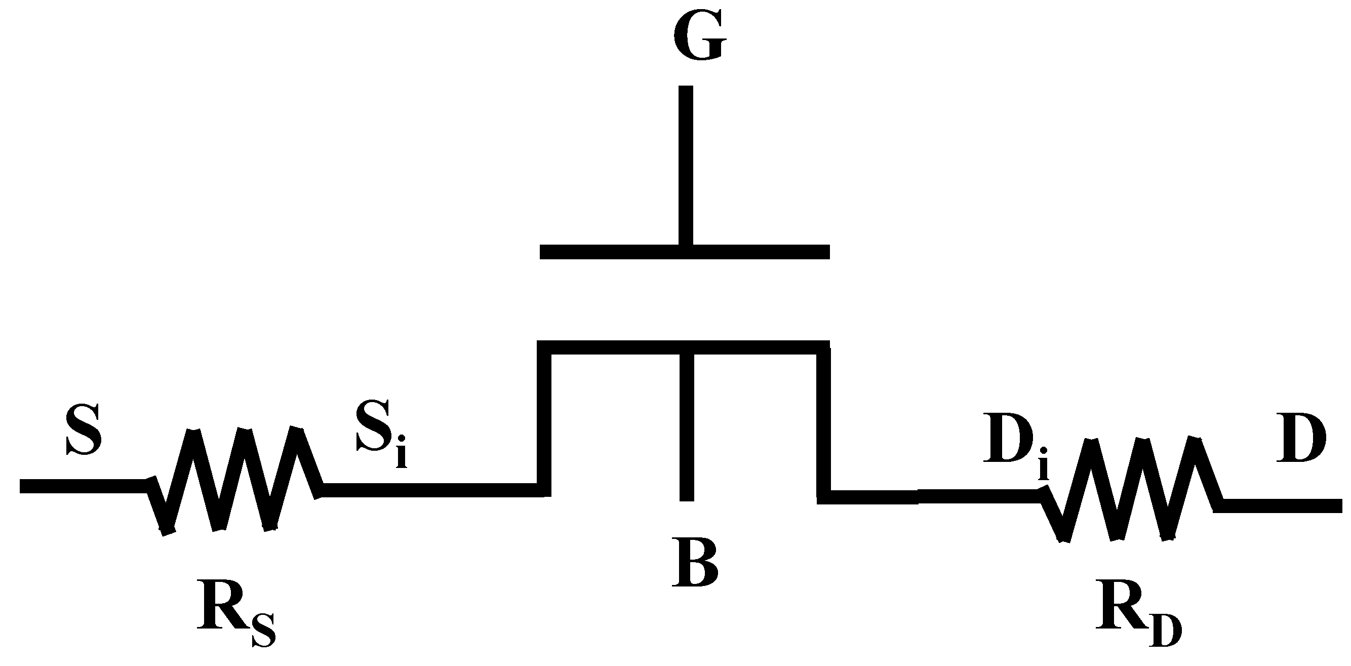
To investigate the influence of the two ferroelectric parameters, tFE and EC, on the transport characteristics of FeFETs and inter-device variations, this study constructs a FeFET model based on a combination of the Preisach ferroelectric model and the MIT Virtual Source (MVS) model. Figure 1a illustrates the two variation sources of interest in this study: the ferroelectric layer thickness, tFE, and the coercive field, EC. Figure 1b shows the three scenarios discussed in this paper: the two ferroelectric parameters fluctuating individually and both fluctuating simultaneously, together with the corresponding assumed Gaussian probability density functions (pdfs) used for Monte Carlo sampling, where both parameters are modeled as Gaussian random variables with standard deviations set to 20% of their mean values. Figure 2 presents the baseline MOSFET structure used in this study and its equivalent modeling framework. The remainder of this article is organized as follows: Section 2 details the device structure and the Preisach–MVS joint modeling method; Section 3 presents the Id-Vg characteristics of FeFET under different ferroelectric parameters, and Monte Carlo statistical analysis is conducted accordingly; and Section 4 summarizes the main conclusions and discusses the application prospects of this modeling in FeFET memory array design.

2.1. Individual MVS and FE Model

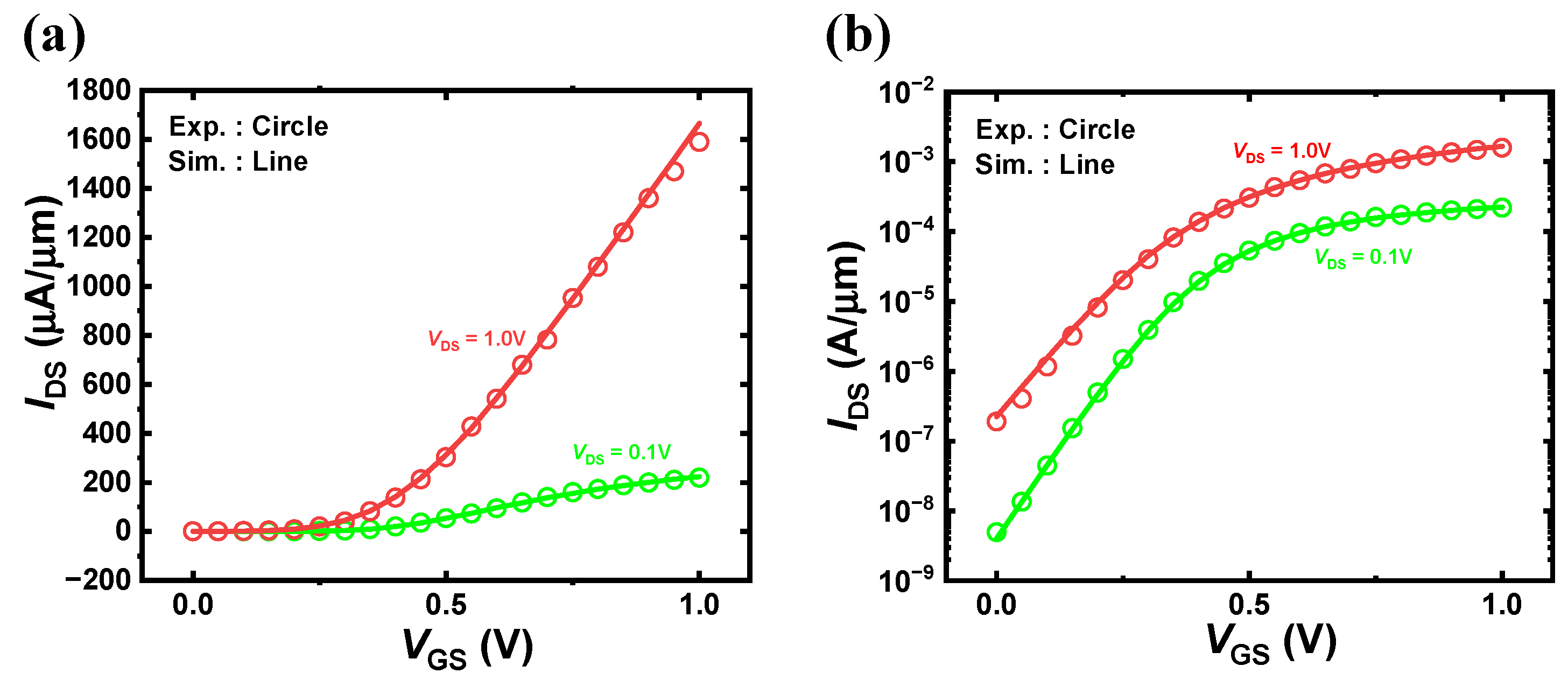
In this study, all FeFET simulations were built upon a common set of baseline metal–oxide–semiconductor field-effect transistor (MOSFET) parameters. To establish a reliable reference at the compact model level, the MVS model [22,23,24,25] was adopted to describe channel transport and calibrate its parameters under the condition of a non-FE gate dielectric to ensure that the simulated Id-Vg characteristics match those of the target device. Although Preisach-type ferroelectric models can be embedded in TCAD platforms for physics-rich simulations, TCAD-based statistical variability analysis becomes computationally prohibitive when hundreds or even thousands of samples are required; therefore, compact Preisach–MVS coupling enables fast DTD statistical evaluation while preserving key physical knobs within a compact model framework. Figure 3 summarizes the calibration results: Figure 3a,b shows the Id-Vg curves in linear and logarithmic scales, respectively. As can be observed, the MVS model agrees well with the reference data [26] in the subthreshold regime, the transition region around the threshold, and the strong inversion regime, thereby accurately capturing key metrics such as turn-on voltage and subthreshold slope.
In subsequent FeFET simulations, the calibrated MVS model is treated as the standard compact model of an ideal MOSFET in the absence of FE effects. Additional variability was not introduced into the baseline transistor. Instead, the focus was put on variations in FE layer parameters. This setup ensures that DTD differences in FeFET characteristics can be attributed to extrinsic variability induced by fluctuations in FE parameters, thereby highlighting the dominant roles played by FE layer thickness and coercive field in the overall DTD variation.

2.2. Preisach–MVS Coupled Model

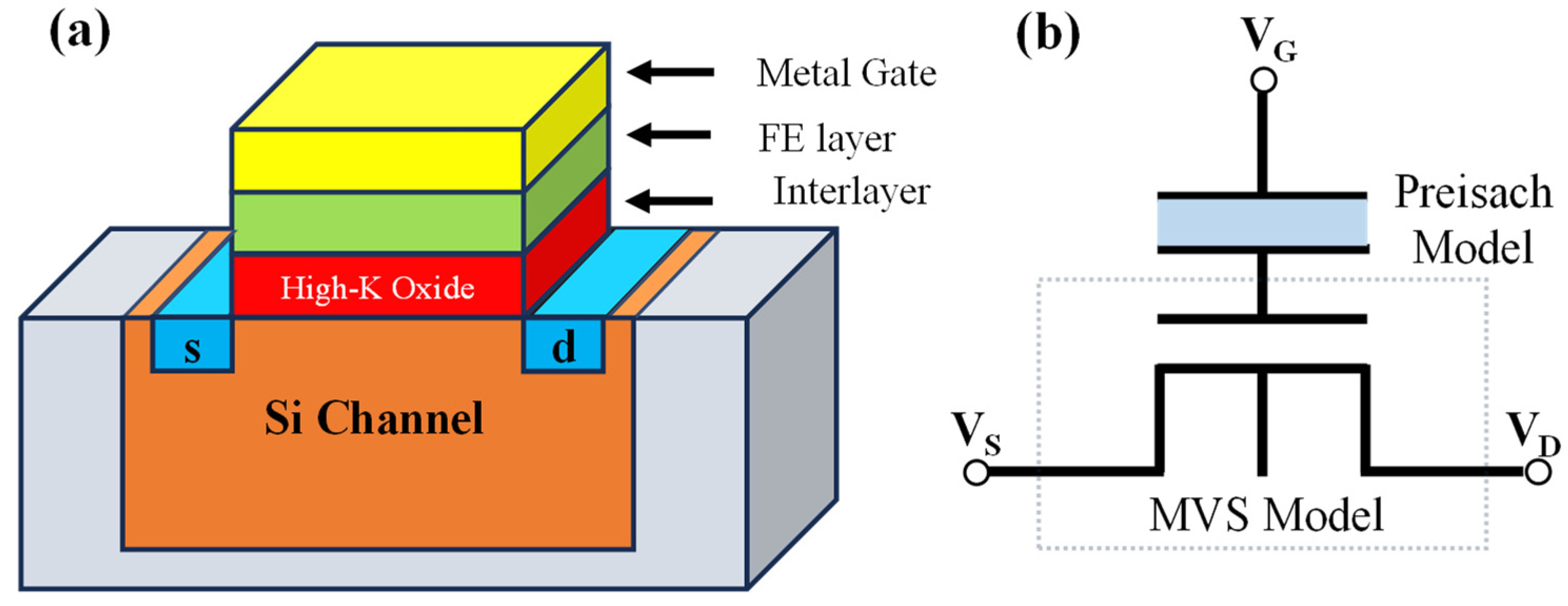
After obtaining the reference MOSFET, an FE thin film was introduced into the gate stack to construct the target FeFET device, as illustrated in Figure 4a. The gate stack from top to bottom consists of a metal gate, an FE layer, a dielectric layer, and the channel. The FE layer thickness, tFE, and coercive field, EC, are considered to be two key variability parameters in this study, which primarily determine the available polarization charge and the threshold electric field required for polarization switching, respectively.
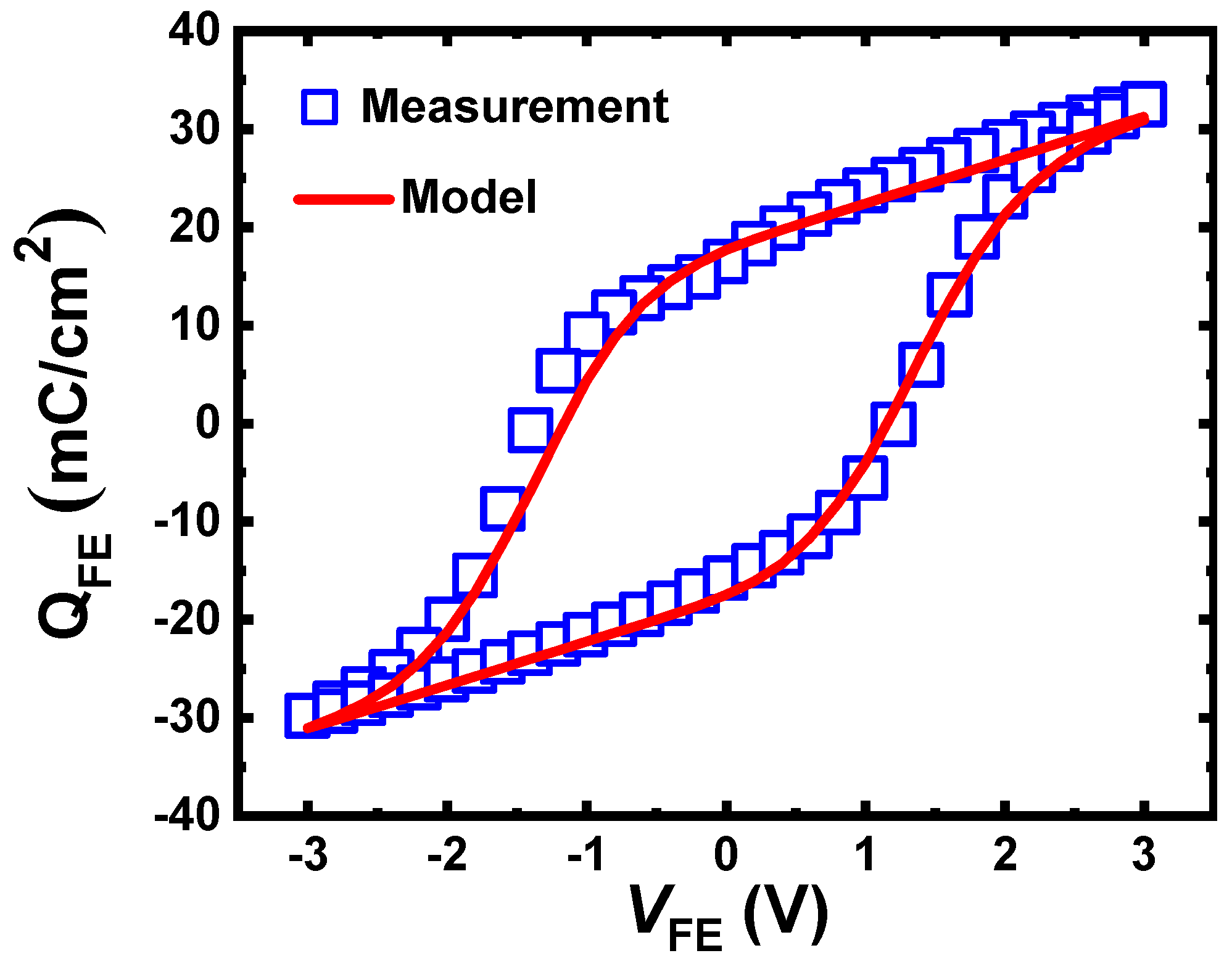
To capture the impact of FE hysteresis on channel conduction within a compact model framework, the Preisach–MVS coupled model was employed, as shown in Figure 4b. The core idea is to represent the FE layer as a multi-domain system composed of a large number of switching units, where each unit switches under a distinct electric field, and the superposition yields a macroscopic hysteresis loop. In the stacked structure, the FE layer is modeled as a nonlinear capacitor in series with the dielectric layer and the channel, and polarization charge is coupled to channel charge via charge conservation. For a given gate voltage, the effective voltage across the FE layer and the corresponding polarization state were first computed, and then the effective voltage was fed into the MVS model to obtain the drain current. In this way, the compact model consistently links polarization switching to variations in surface potential and channel current [27,28,29]. To ensure quantitative fidelity of the ferroelectric stack before performing variability analysis, we calibrate the Preisach ferroelectric parameters against the measured QFE–VFE hysteresis loop of a metal–ferroelectric–metal (MFM) capacitor. Figure 5 compares the measured loop with the fitted Preisach result, showing that the loop shape and switching characteristics are well reproduced. This calibration strategy first fits the FE capacitor hysteresis, and then uses the calibrated FE response in the coupled device model. It is also consistent with experimentally calibrated FeFET compact-modeling studies reported in the literature, where calibrated models are validated against measured device-level trends and variability behaviors [18].
Then, the low-threshold voltage VTH_L and high-threshold voltage VTH_H were extracted from the two curves using the constant-current method, and MW was defined as follows:
M W = V T H _ H V T H _ L .
For each set of FE parameters, a full bidirectional sweep is conducted to extract VTH_H, VTH_L, and MW. In the subsequent sensitivity analysis, only one FE parameter is varied at a time to evaluate its impact. In the variability analysis, tFE and EC are simultaneously perturbed following Gaussian distributions, and MC simulations are performed to obtain the statistical distributions of VTH and MW. Accordingly, throughout this study we extract the MW from quasi-static DC Id-Vg hysteresis sweeps. This MW corresponds to the saturated window under the implicit assumption that the applied gate bias amplitude and sweep condition are sufficient to complete polarization switching in the ferroelectric layer. Under finite-duration programming pulses, the apparent MW additionally depends on pulse amplitude and pulse width through switching dynamics; such time-dependent effects are not considered here because this study focuses on static characteristics. In addition to tFE and EC, remanent polarization can also influence MW. However, in this study we do not treat polarization amplitude as an independent random variable, because it is strongly correlated with FE thickness in HfO2-based thin films. For example, experimental studies on ultrathin doped HfO2 report a pronounced thickness dependence of polarization switching, including a sharp reduction in switchable polarization when the film thickness is scaled below a critical value [30]. Therefore, in our Monte Carlo setup, varying tFE naturally serves as a practical proxy that implicitly captures the correlated fluctuation in polarization amplitude, avoiding potential double counting of strongly coupled parameters.

3. Results

3.1. Parameter Dependence on FeFET Performance

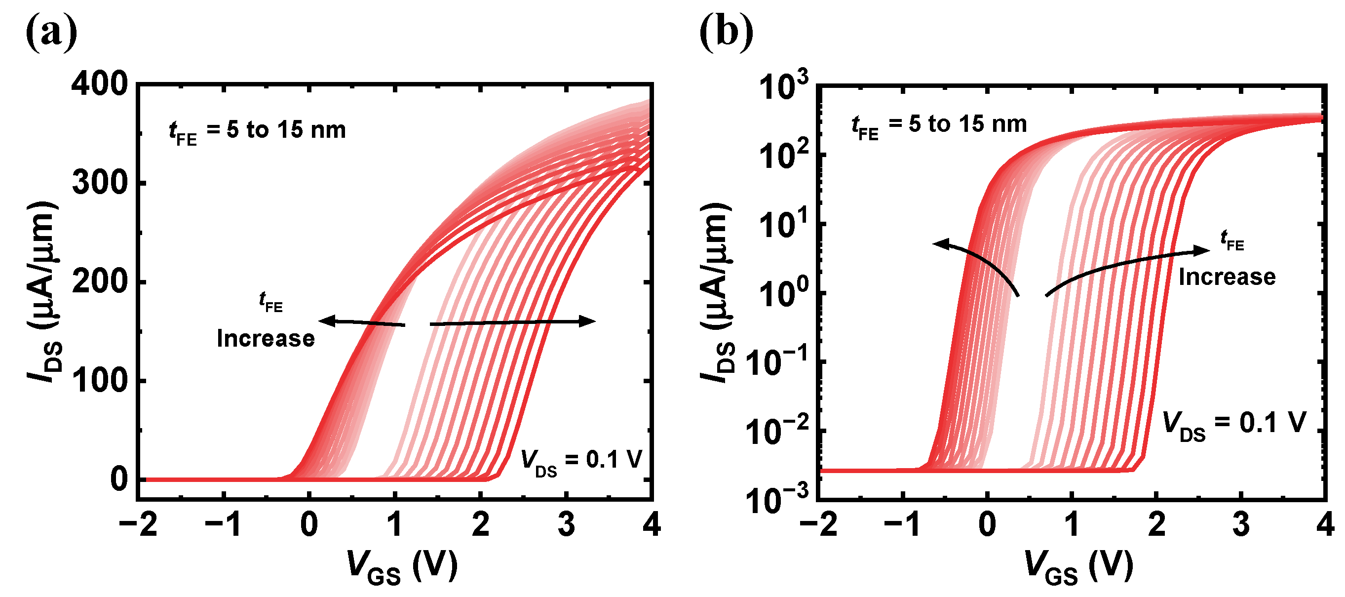
Figure 6 shows the simulated FeFET Id-Vg characteristics under different FE layer thicknesses (tFE), where Figure 6a,b is plotted in linear and logarithmic scales, respectively. As tFE increases, the drain current exhibits a clear change in both the turn-on region and the strong inversion region. Specifically, a thicker FE layer shifts the VTH_H branch toward more positive gate bias, while shifting the VTH_L branch toward more negative gate bias. This enlarges the horizontal separation between the two branches, i.e., a wider MW. Meanwhile, in the strong inversion regime, the on-current difference between the two branches becomes increasingly pronounced with tFE. In contrast, the subthreshold slope shows only minor variations across different tFE, indicating that within the considered parameter range the impact of tFE on subthreshold swing is limited. This behavior can be understood as tFE primarily modulates the threshold position by altering the effective input voltage coupled with the MVS channel model.
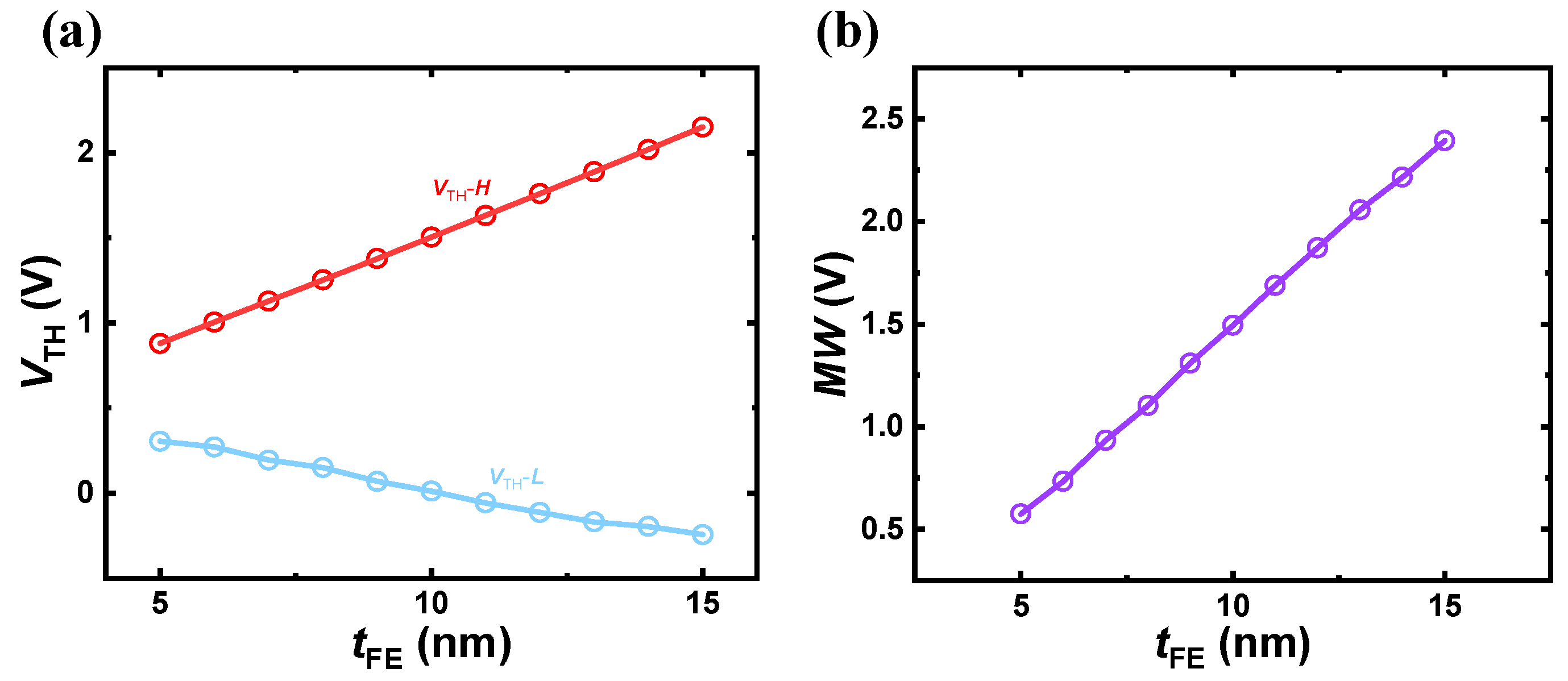
To quantify these trends more explicitly, Figure 7 summarizes the extracted threshold voltages and MW as functions of tFE based on Figure 5. As shown in Figure 6a, VTH_L decreases slightly with increasing tFE, whereas VTH_H increases markedly; consequently, their difference (MW) increases approximately linearly, as shown in Figure 6b. Physically, under the same gate–voltage sweep range, a thicker FE layer can support a larger accumulated polarization charge. After coupling through the gate stack, this leads to a larger effective modulation of channel charge, thereby producing a more pronounced separation of the two switching branches and ultimately a wider MW. However, further increasing tFE also raises the gate voltage required to complete polarization switching. This not only increases power consumption but may also elevate the electric field stress in the dielectric layer, potentially introducing reliability concerns such as dielectric breakdown. Therefore, practical design requires a trade-off between achieving a sufficiently large MW and maintaining an acceptable operating voltage.
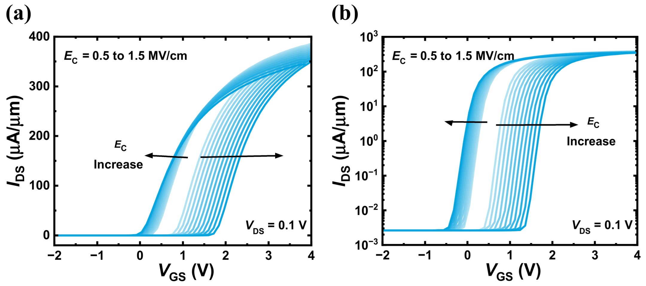
Figure 8 presents the FeFET Id-Vg characteristics under different coercive fields (EC). Similar to the effect of tFE, increasing EC enlarges the hysteresis width: the VTH_H branch shifts toward more positive gate bias, while the VTH_L branch shifts toward more negative gate bias, resulting in an expanded MW. Different from thickness scaling, EC mainly determines the critical voltage required for polarization switching, and thus more directly affects the overall position of the hysteresis loop along the gate–voltage axis. With a larger EC, the FE layer tends to remain in its initial polarization state over a wider gate–voltage range; switching occurs only after the applied bias exceeds the new critical value, which manifests as a systematic shift in the Id-Vg curves.
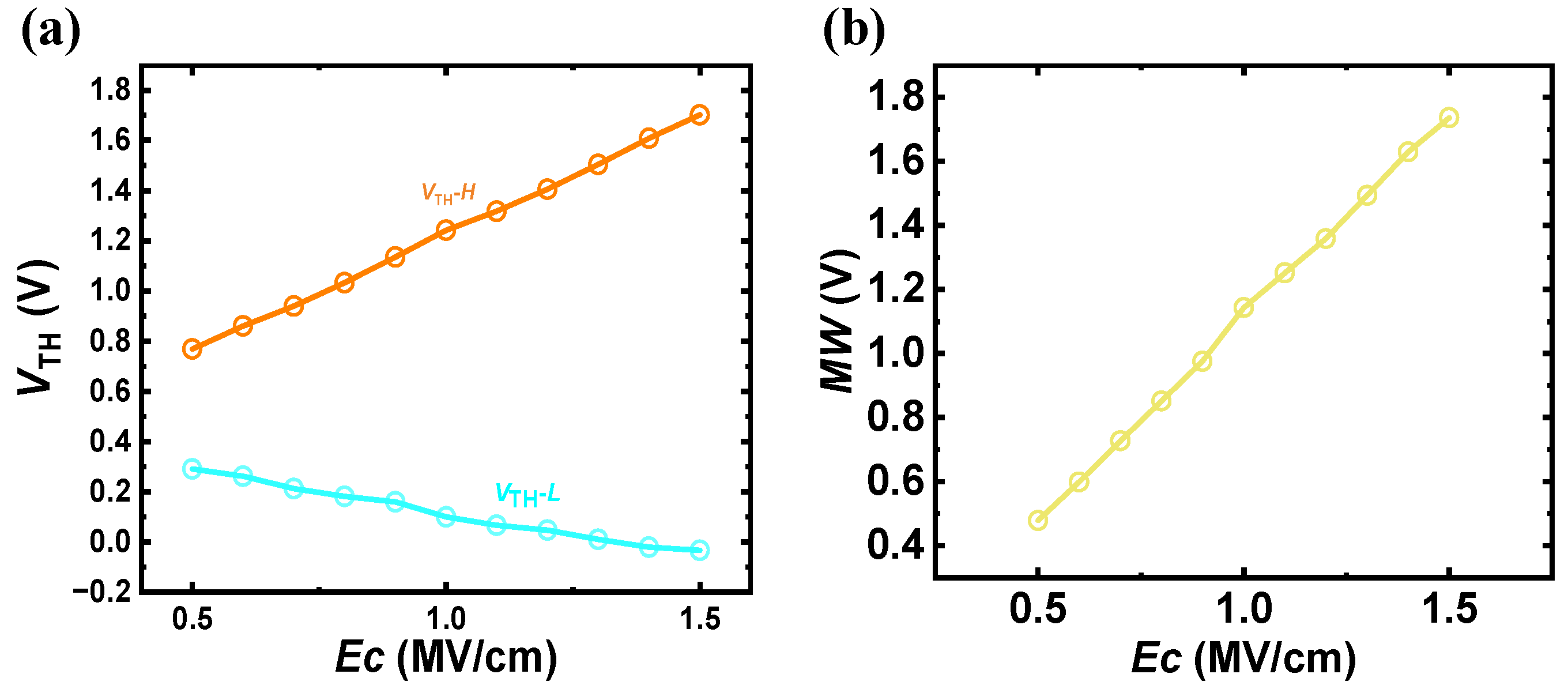
Figure 9 further shows the extracted VTH and MW as functions of EC from Figure 7. The trends are similar across different tFE cases: VTH_L changes with a relatively small slope, whereas VTH_H increases with a much larger slope; correspondingly, MW increases approximately linearly with EC, as shown in Figure 8b. Compared with EC sweeping, varying tFE within a similar relative range produces a more pronounced change in MW, indicating that MW is more sensitive to tFE than to EC under the conditions considered. Overall, both tFE and EC can substantially influence the static characteristics of FeFETs: increasing either parameter can enlarge MW, but this also shifts the threshold-voltage positions and modifies the drain-current levels. These observations serve as the basis for the subsequent DTD variability analysis.

3.2. Analysis of DTD Variations

In this section, MC simulations were conducted to analyze three variability scenarios: (i) tFE variation only; (ii) EC variation only; and (iii) simultaneous variations in both tFE and EC. For each scenario, the nominal values of the FE parameters are used as the means, while the standard deviation is set to 20% of the mean. This 20% fluctuation range is a commonly used setting in TCAD or compact model-based variability studies to represent a reasonable level of process-induced variations. For example, researchers explicitly target lithography-induced gate-length dispersion and take L g fluctuation as the sole random variable; they apply a ±10% variation around the nominal L g and propagate this process variation through Monte Carlo sampling to evaluate circuit-level robustness. Under this setting, the simulated NOR gate still shows correct logic functionality and no observable hysteresis within the target window, enabling a meaningful statistical assessment of propagation-delay variability [31]. This study randomly generated 100 samples, simulated a complete hysteretic Id-Vg characteristic for each sample, and extracted VTH_L, VTH_H, and MW. Although 100 samples may appear modest, this already falls into the “hundred-level statistics” regime that is commonly adopted for DTD variability benchmarking, where distribution-level metrics such as the coefficient of variation are extracted to draw robust conclusions and guide optimization. As discussed by Lanza et al., variability studies of key FET figures of merit, such as threshold voltage and subthreshold swing, are typically carried out on hundreds of devices to obtain statistically meaningful trends [32]. In this context, using N = 100 Monte Carlo samples in each scenario provides an effective and computationally efficient basis for comparing the extracted mean, standard-deviation and COV across different variation cases; meanwhile, larger N can be used in a straightforward way if tighter confidence bounds are required.
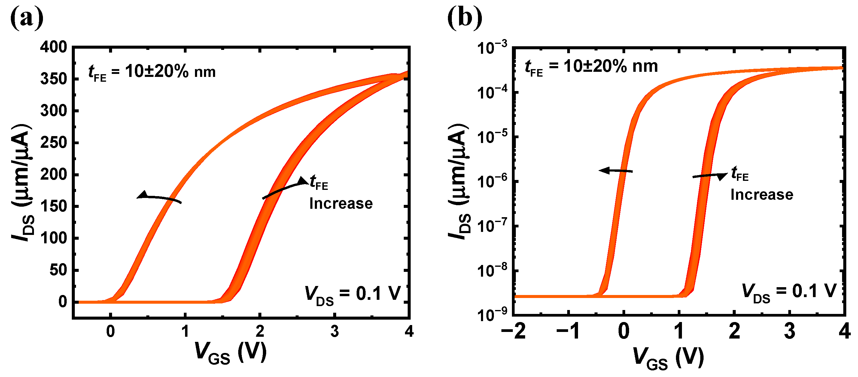
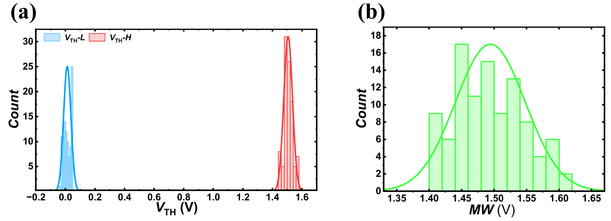
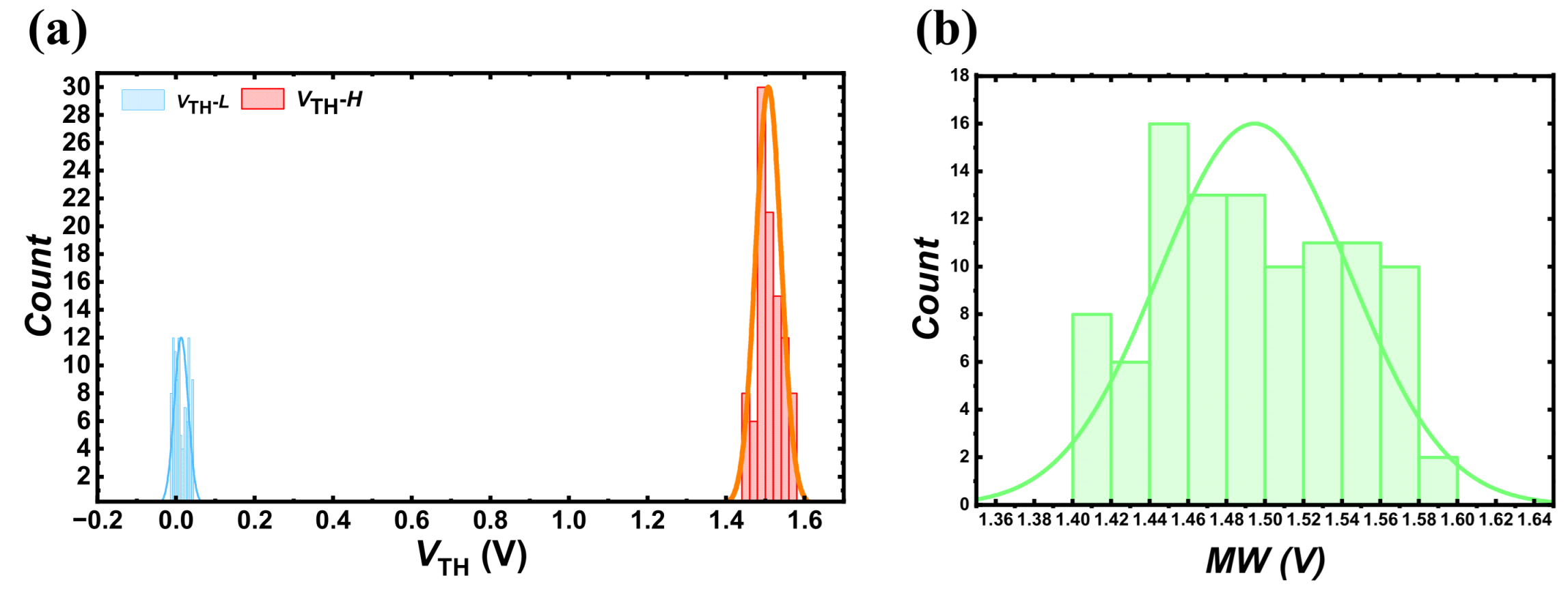
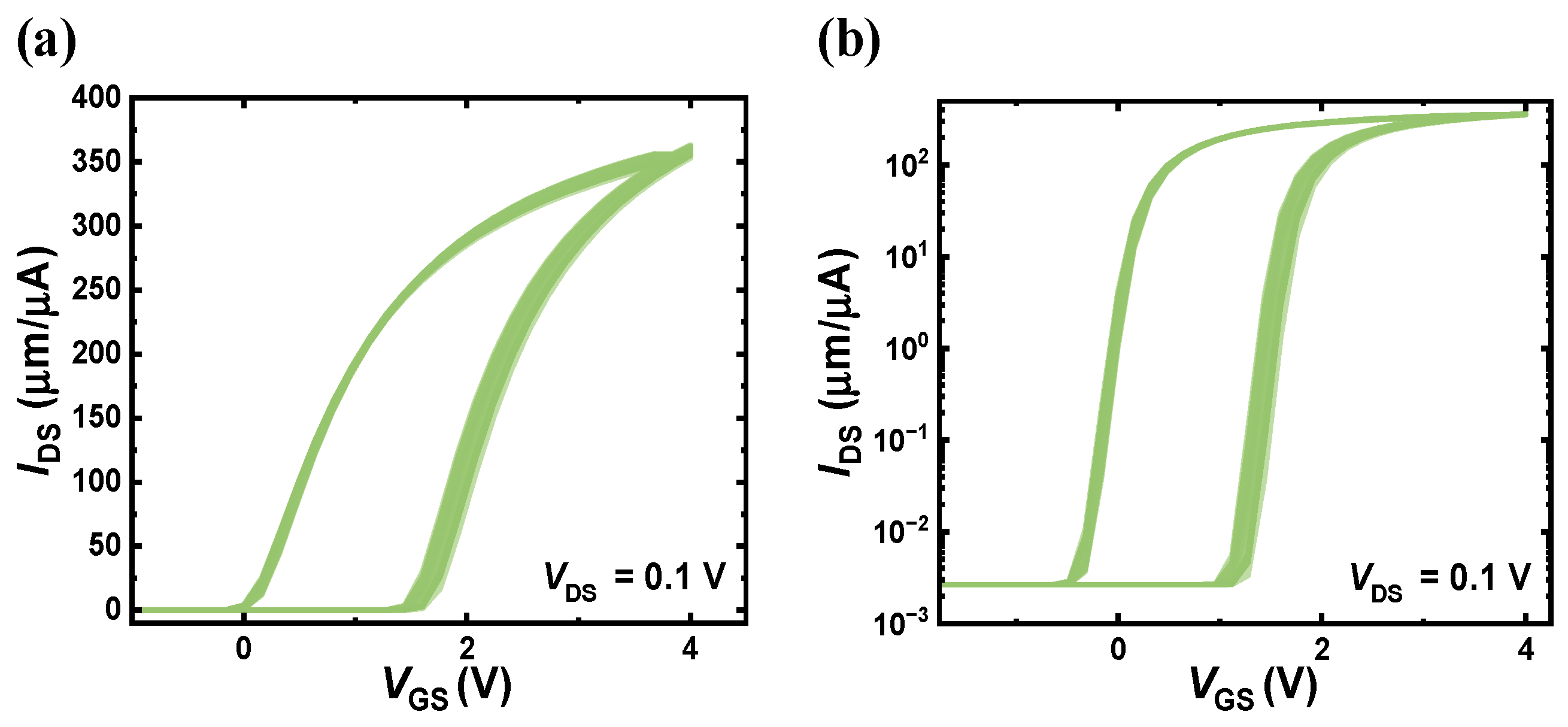
Figure 10a,b shows the Id-Vg hysteresis curves of 100 samples when only tFE varies, plotted in linear and logarithmic scales, respectively. It can be observed that the curves largely overlap in the subthreshold regime, whereas a certain horizontal spread appears near the threshold region and in strong inversion; however, the overall dispersion remains limited. Figure 10 further presents the corresponding statistical histograms of threshold voltages and MW. In Figure 11a, both VTH_L and VTH_H approximately follow Gaussian distributions, with mean values of ~0.01 V and ~1.51 V and standard deviations of 25 mV and 30 mV, respectively. Figure 11b shows that MW also follows an approximately Gaussian distribution, with a mean of 1.49 V and a standard deviation of 54 mV. These results indicate that even with a 20% fluctuation in thickness, the high/low threshold voltages and MW exhibit observable DTD dispersions, while the overall spread is constrained to the order of tens of millivolts.
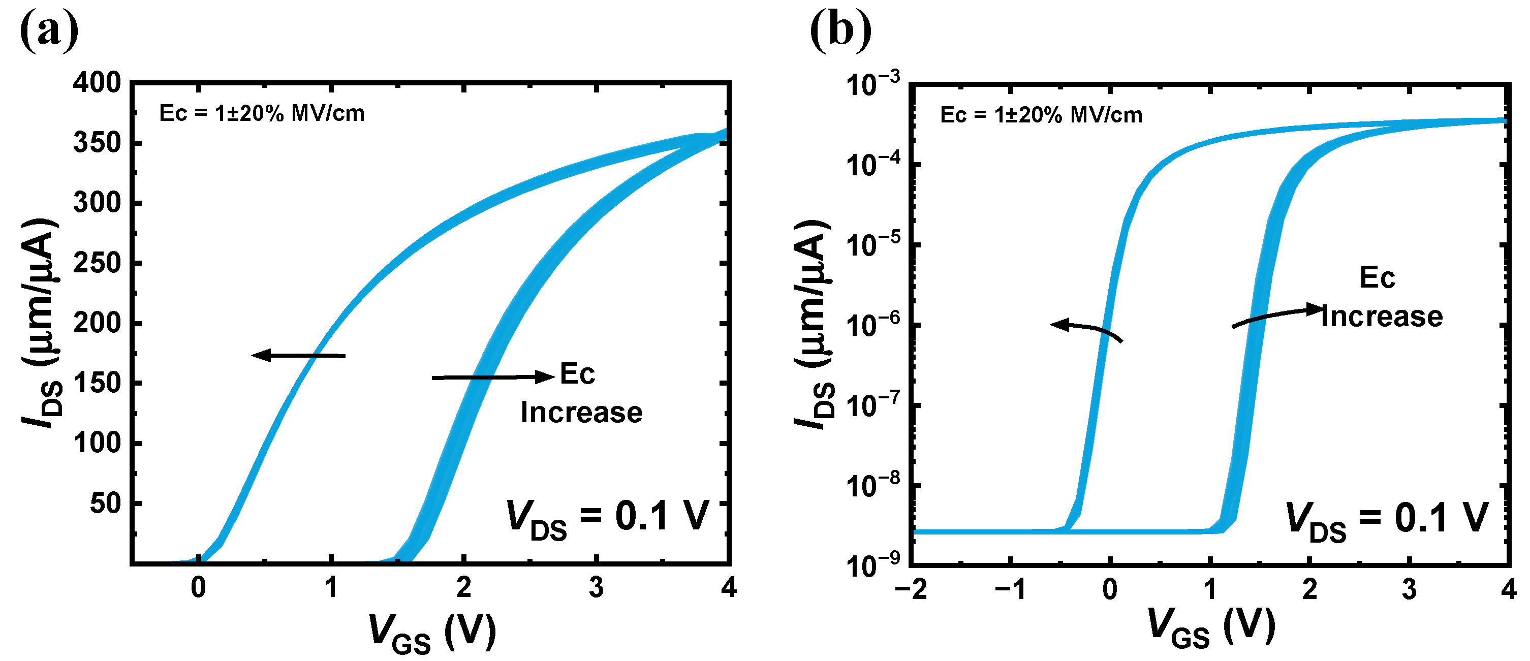
Next, this study considered the scenario where only EC varies. Figure 12a,b show the Id-Vg hysteresis curves of 100 samples under EC variation in linear and logarithmic scales. The random fluctuation in EC primarily manifests as a translation of the hysteresis curves along the Vg axis. When EC is smaller, the VTH_L branch shifts toward more positive gate bias while the VTH_H branch shifts toward more negative gate bias, leading to a reduced MW. Conversely, when EC is larger, the VTH_L branch shifts toward more negative gate bias and the VTH_H branch shifts toward more positive gate bias, resulting in an enlarged MW. Importantly, the turn-on behavior and the drain current in strong inversion remain largely unchanged across samples. Figure 13a,b summarizes the extracted statistics: VTH_L and VTH_H still follow approximately Gaussian distributions with mean values of 0.013 V and 1.51 V and standard deviations of 18 mV and 32 mV, respectively, while MW has a mean of 1.49 V and a standard deviation of ~50 mV. Overall, within the prescribed 20% variability range, tFE-only and EC-only cases lead to DTD dispersions of comparable magnitude in both threshold voltage and MW.
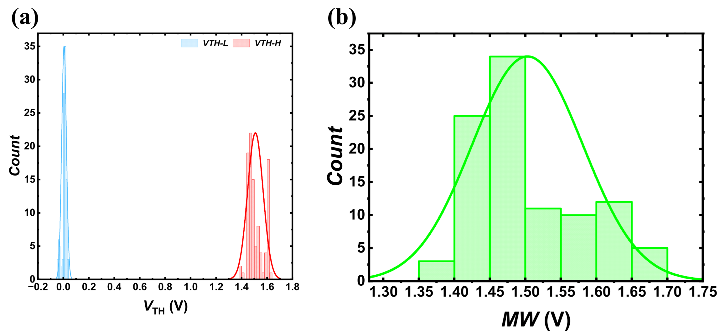
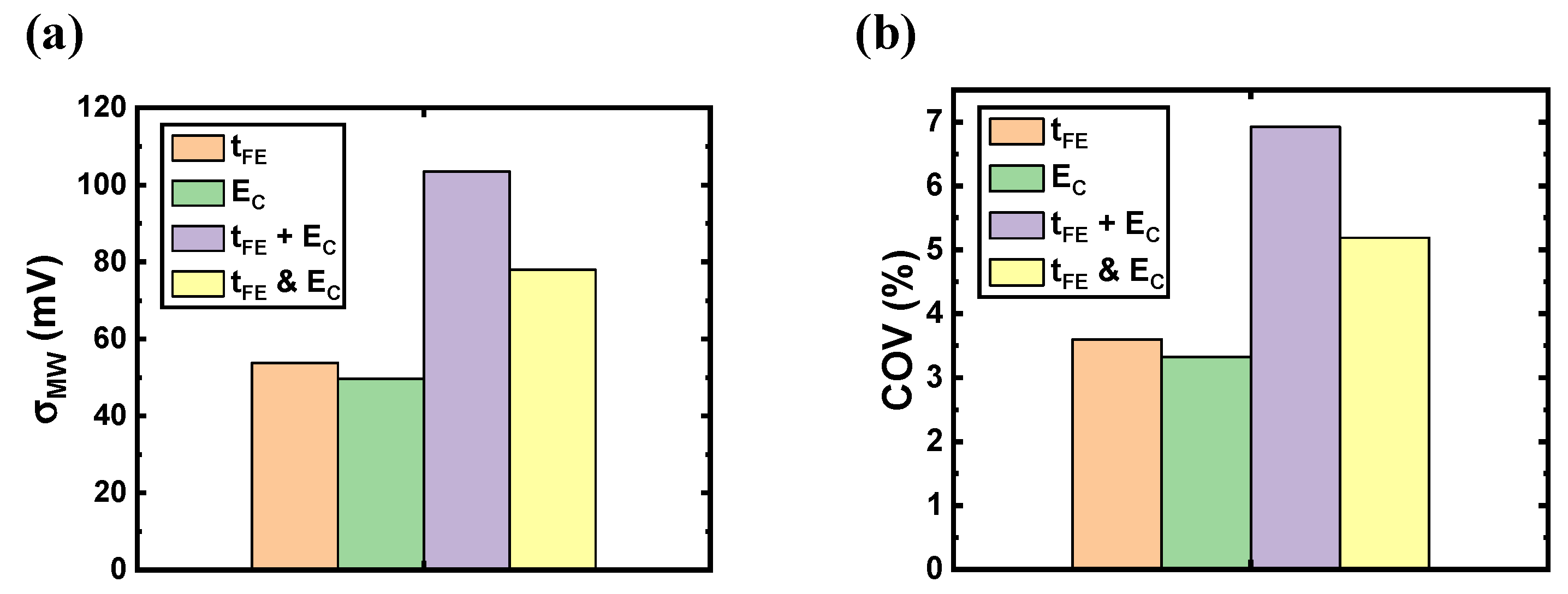
When tFE and EC vary simultaneously, DTD variability is further amplified. Figure 14a,b show the Id-Vg hysteresis curves of 100 samples when both parameters fluctuate with a 20% standard deviation. The envelope of curves near the threshold region becomes substantially wider: the locations of the VTH_H and VTH_L branches exhibit pronounced scattering across samples, and the branch separation (i.e., MW) also shows a larger fluctuation. The corresponding histograms in Figure 15a,b indicate that VTH_L and VTH_H have mean values of 0.006 V and 1.51 V, with standard deviations of 18 mV and 61 mV, respectively, while MW has a mean of 1.50 V and a standard deviation of 78 mV. Therefore, when thickness and coercive-field variations coexist, the dispersions of threshold voltage and MW become significantly larger than those induced by either single-parameter variation, exceeding the expectation from a simple linear superposition and indicating a synergistic amplification of DTD variability. This observed synergistic amplification originates from the fact that tFE and EC affect the two hysteresis branches through coupled mechanisms in the Preisach–MVS stack. On the one hand, varying tFE changes the amount of polarization charge that can be accumulated and coupled to the channel, thereby modulating the effective input voltage seen by the MVS channel model and shifting the extracted threshold positions. On the other hand, EC mainly sets the critical bias required for polarization switching, which manifests as a translation of the hysteresis loop along the Vg axis. Importantly, these effects are not independent: in a series-stacked gate, the branch transition points that define VTH_H and VTH_L are governed simultaneously by how strongly polarization charge shifts the channel and how much gate bias is needed to complete the branch switching. Therefore, when tFE and EC fluctuate together, the branch positions can be perturbed in a correlated manner, producing a broader spread than the simple linear superposition of single-parameter cases. This is consistent with the extracted statistics, where the joint-variation case yields a much larger standard deviation of VTH and MW compared with the t F E -only and E C -only cases, while the mean values remain almost unchanged. Figure 16a,b summarize the extracted dispersion metrics across the three scenarios. In terms of the standard deviation and coefficient of variation (COV) [33,34], the joint-variation case exhibits a substantially larger spread than either single-variation case. In summary, under the statistical range considered in this study, FeFET DTD variability is dominated by the coupled fluctuations of tFE and EC. This suggests that, at both the device and circuit levels, reducing the statistical dispersions of tFE and EC is essential for improving the reliability of large-scale FeFET arrays.

4. Conclusions

This study develops a coupled compact model for FeFETs by integrating the Preisach FE model with the MVS MOSFET model. The impacts of FE layer thickness, tFE, and coercive field, EC, on device performance and DTD variations have been systematically investigated. The results show that increasing either tFE or EC can significantly enlarge the MW. Under a 20% relative fluctuation, the case where tFE and EC vary simultaneously leads to substantially larger dispersions in VTH and MW than (i) either single variability source alone and (ii) the direct superposition of their individual effects, indicating a pronounced synergistic amplification. Owing to its low computational cost and clear physical interpretability, the proposed model provides an efficient approach to evaluating VTH distributions and read/write margins in FeFET arrays under realistic process fluctuations. It also serves as a foundation for incorporating additional process-variation sources to further optimize next-generation FE memory arrays.

Author Contributions

Conceptualization, Z.L. (Ziang Li), W.H. and Z.L. (Zhanqi Liu); Methodology, Z.L. (Ziang Li), W.H. and Z.L. (Zhanqi Liu); Validation, Z.L. (Ziang Li), W.H. and Z.L. (Zhanqi Liu); Formal analysis, Z.L. (Ziang Li), W.H. and Z.L. (Zhanqi Liu); Investigation, Z.L. (Ziang Li), W.H. and Z.L. (Zhanqi Liu); Writing—original draft, Z.L. (Ziang Li), W.H. and Z.L. (Zhanqi Liu); Writing—review & editing, Z.L. (Ziang Li), W.H. and Z.L. (Zhanqi Liu); Visualization, Z.L. (Ziang Li), W.H. and Z.L. (Zhanqi Liu). All authors have read and agreed to the published version of the manuscript.

Funding

This research was funded by the Special Fund for Central Government Guiding Local Science and Technology Development (24ZYQA050) and the Science and Technology Program of Gansu Province (24ZDFA006).

Data Availability Statement

The raw data supporting the conclusions of this article will be made available by the authors on request.

Acknowledgments

This study was partly supported by the Special Fund for Central Government Guiding Local Science and Technology Development (24ZYQA050) and the Science and Technology Program of Gansu Province (24ZDFA006). This study was supported by the Supercomputing Center of Lanzhou University.

Conflicts of Interest

The authors declare no conflicts of interest.

References

  1. Böscke, T.S.; Müller, J.; Bräuhaus, D.; Schröder, U.; Böttger, U. Ferroelectricity in hafnium oxide thin films. Appl. Phys. Lett. 2011, 99, 102903. [Google Scholar] [CrossRef]
  2. Polakowski, P.; Müller, J. Ferroelectricity in undoped hafnium oxide. Appl. Phys. Lett. 2015, 106, 232905. [Google Scholar] [CrossRef]
  3. MPark, H.; Lee, Y.H.; Mikolajick, T.; Schroeder, U.; Hwang, C.S. Review and perspective on ferroelectric HfO2-based thin films for memory applications. MRS Commun. 2018, 8, 795–808. [Google Scholar]
  4. Trentzsch, M.; Flachowsky, S.; Richter, R.; Paul, J.; Reimer, B.; Utess, D.; Jansen, S.; Mulaosmanovic, H.; Muller, S.; Slesazeck, S.; et al. A 28 nm HKMG super low power embedded NVM technology based on ferroelectric FETs. In Proceedings of the 2016 IEEE International Electron Devices Meeting (IEDM), San Francisco, CA, USA, 3–7 December 2016; pp. 294–297. [Google Scholar]
  5. Wang, J.; Zhang, W.; Wu, Z.; Wang, Y.; Jiao, L.; Wang, X.; Gong, X.; Fong, X. Transposable memory based on the ferroelectric field-effect transistor. In Proceedings of the 2024 IEEE International Symposium on Circuits and Systems (ISCAS), Singapore, 19–22 May 2024; pp. 22.6.1–22.6.4. [Google Scholar] [CrossRef]
  6. Ali, T.; Polakowski, P.; Riedel, S.; Buttner, T.; Kampfe, T.; Rudolph, M.; Patzold, B.; Seidel, K.; Lohr, D.; Hoffmann, R.; et al. High endurance ferroelectric hafnium oxide-based FeFET memory without retention penalty. IEEE Trans. Electron Devices 2018, 65, 3769–3774. [Google Scholar] [CrossRef]
  7. Zeng, B.; Liao, M.; Peng, Q.; Xiao, W.; Liao, J.; Zheng, S.; Zhou, Y. A high-density 2-bit/cell operation ferroelectric FET memory based on Hf0.5Zr0.5O2 for NAND applications. IEEE J. Electron Devices Soc. 2019, 7, 551–556. [Google Scholar] [CrossRef]
  8. Mikolajick, T.; Slesazeck, S.; Park, M.H.; Schroeder, U. The past, the present, and the future of ferroelectric memories. IEEE Trans. Electron Devices 2020, 67, 1434–1443. [Google Scholar] [CrossRef]
  9. Wang, J.; Zhang, W.; Fong, X. A Failure Analysis Framework for Ferroelectric Field-Effect Transistor Memory. In Proceedings of the 2024 IEEE International Conference on IC Design and Technology (ICICDT), Singapore, 25–27 September 2024; pp. 1–4. [Google Scholar]
  10. Ni, K.; Gupta, A.; Prakash, O.; Thomann, S.; Hu, X.S.; Amrouch, H. Impact of extrinsic variation sources on the device-to-device variation in ferroelectric FET. In Proceedings of the 2020 IEEE International Reliability Physics Symposium (IRPS), Virtual, 28 April–30 May 2020; pp. 1–5. [Google Scholar]
  11. Wang, J.; Zhang, W.; Fong, X. A Bit-Cell Failure Analysis Framework For Ferroelectric Field-Effect Transistor-Based Memories. IEEE J. Explor. Solid-State Comput. Devices Circuits 2025, 11, 123–130. [Google Scholar] [CrossRef]
  12. Choe, G.; Yu, S. Variability study of ferroelectric field-effect transistors towards 7 nm technology node. IEEE J. Electron Devices Soc. 2021, 9, 1131–1136. [Google Scholar] [CrossRef]
  13. Dastgeer, G.; Nisar, S.; Zulfiqar, M.W.; Eom, J.; Imran, M.; Akbar, K. A review on recent progress and challenges in high-efficiency perovskite solar cells. Nano Energy 2024, 132, 110401. [Google Scholar] [CrossRef]
  14. Dastgeer, G.; Zulfiqar, M.W.; Nisar, S.; Zulfiqar, R.; Imran, M.; Panchanan, S.; Dutta, S.; Akbar, K.; Vomiero, A.; Wang, Z. Emerging role of 2D materials in photovoltaics: Efficiency enhancement and future perspectives. Nano-Micro Lett. 2026, 18, 32. [Google Scholar] [CrossRef]
  15. Thomann, S.; Mulaosmanovic, H.; Ni, K.; Amrouch, H. Reliable FeFET-based neuromorphic computing through joint modeling of cycle-to-cycle variability, device-to-device variability, and domain stochasticity. In Proceedings of the 2023 IEEE International Reliability Physics Symposium (IRPS), Monterey, CA, USA, 26–30 March 2023. [Google Scholar]
  16. Zhang, W.; Xie, Y.; Wang, J.; Fong, X. 3D Phase Field Simulation and Variability Analysis of Polycrystalline Ferroelectric Memories. In Proceedings of the 2024 IEEE International Conference on IC Design and Technology (ICICDT), Singapore, 25–27 September 2024; pp. 1–4. [Google Scholar]
  17. Zhang, W.; Wang, J.; Fong, X. Polar-Axis Orientation Fluctuations and the Impact on the Intrinsic Variability in Ferroelectric Capacitors. IEEE J. Explor. Solid-State Comput. Devices Circuits 2025, 11, 74–80. [Google Scholar] [CrossRef]
  18. Deng, S.; Yin, G.; Chakraborty, W.; Dutta, S.; Datta, S.; Li, X.; Ni, K. A comprehensive model for ferroelectric FET capturing the key behaviors: Scalability, variation, stochasticity, and accumulation. In Proceedings of the 2020 Symposium on VLSI Technology (VLSI Technology), Virtual, 16–19 June 2020; pp. 1–2. [Google Scholar]
  19. Zhang, W.; Fong, X. A Comprehensive Variability Modeling Framework for Oxide Semiconductor Channel-Based Ferroelectric Thin Film Transistors. In Proceedings of the 2025 IEEE International Compact Modeling Conference (ICMC), San Francisco, CA, USA, 26–27 June 2025; pp. 1–4. [Google Scholar]
  20. Garg, C.; Chauhan, N.; Deng, S.; Khan, A.I.; Dasgupta, S.; Bulusu, A.; Ni, K. Impact of random spatial fluctuation in non-uniform crystalline phases on the device variation of ferroelectric FET. IEEE Electron Device Lett. 2021, 42, 1160–1163. [Google Scholar] [CrossRef]
  21. Ni, K.; Chakraborty, W.; Smith, J.A.; Grisafe, B.; Datta, S. Fundamental understanding and control of device-to-device variation in deeply scaled ferroelectric FETs. In Proceedings of the 2019 Symposium on VLSI Technology (VLSI Technology), Kyoto, Japan, 9–14 June 2019; pp. T40–T41. [Google Scholar]
  22. Khakifirooz, A.; Antoniadis, D.A. A simple semiempirical short-channel MOSFET current–voltage model continuous across all regions of operation and employing only physical parameters. IEEE Trans. Electron Devices 2009, 56, 1674–1680. [Google Scholar] [CrossRef]
  23. Zhang, W. Understanding and Modelling of the Advanced Transistor at Extremely Scaled Channel Length using Virtual Source Model. Res. Sq. 2025; preprint. [Google Scholar]
  24. Rakheja, V.; Khakifirooz, A.; Hashemi, P.; Antoniadis, D.A. An improved virtual-source-based transport model for quasi-ballistic transistors—Part I: Capturing effects of carrier degeneracy. IEEE Trans. Electron Devices 2015, 62, 2786–2793. [Google Scholar] [CrossRef]
  25. Rakheja, V.; Khakifirooz, A.; Hashemi, P.; Antoniadis, D.A. An improved virtual-source-based transport model for quasi-ballistic transistors—Part II: Experimental verification. IEEE Trans. Electron Devices 2015, 62, 2794–2801. [Google Scholar] [CrossRef]
  26. Mistry, K.; Allen, C.; Auth, C.; Beattie, B.; Bergstrom, D.; Bost, M.; Brazier, M.; Buehler, M.; Cappellani, A.; Chau, R.; et al. A 45nm Logic Technology with High-k+Metal Gate Transistors, Strained Silicon, 9 Cu Interconnect Layers, 193 nm Dry Patterning, and 100% Pb-free Packaging. In Proceedings of the International Electron Devices Meeting (IEDM), Washington, DC, USA, 10–12 December 2007; pp. 247–250. [Google Scholar]
  27. Zhang, W.; Wang, J.; Sun, C.; Wu, Z.; Gong, X.; Fong, X. Modeling of ferroelectric thin film transistors with amorphous oxide semiconductor channel. In Proceedings of the 2024 8th IEEE Electron Devices Technology and Manufacturing (EDTM) Conference, Bangalore, India, 3–6 March 2024; pp. 1–3. [Google Scholar]
  28. Zhang, W.; Wang, J.; Sun, C.; Kong, Q.; Wu, Z.; Gong, X.; Fong, X. A Compact Model for BEOL-Compatible Ferroelectric Thin Film Transistors With Metal/Ferroelectric/Semiconductor Structure. IEEE J. Electron Device Soc. 2025, 13, 745–755. [Google Scholar] [CrossRef]
  29. Tung, C.-T.; Pahwa, G.; Salahuddin, S.; Hu, C. A Compact Model of Ferroelectric Field-Effect Transistor. IEEE Electron Device Lett. 2022, 43, 1363–1366. [Google Scholar] [CrossRef]
  30. Tian, X.; Shibayama, S.; Nishimura, T.; Yajima, T.; Migita, S.; Toriumi, A. Evolution of ferroelectric HfO2 in ultrathin region down to 3 nm. Appl. Phys. Lett. 2018, 112, 102902. [Google Scholar] [CrossRef]
  31. Qiu, Y.; Kang, L. Design and Robustness Analysis of a NOR Logic Gate Based on Complementary Negative-Capacitance Field-Effect Transistors. In Proceedings of the 2025 5th International Conference on Electrical Engineering and Control Science (IC2ECS), Beijing, China, 5–7 December 2025; IEEE: New York, NY, USA; Volume 2025, pp. 710–713.
  32. Lanza, M.; Smets, Q.; Huyghebaert, C.; Li, L.-J. Yield, variability, reliability, and stability of two-dimensional materials based solid-state electronic devices. Nat. Commun. 2020, 11, 5689. [Google Scholar] [CrossRef] [PubMed]
  33. Zhang, W.; Sun, C.; Li, X.; Wang, Z.; Wang, J.; Cen, Y.; Zhang, D.; Du, T.; Lu, Y.; Gong, X.; et al. Multi-Grain Ferroelectric Induced Drain Current Variability in BEOL-Compatible OS FeFETs. IEEE Electron Device Lett. 2025, 1–4. [Google Scholar] [CrossRef]
  34. Du, T.; Zhang, W.; Fong, X.; Hu, G.; Zhou, P.; Lu, Y. Comprehensive Modeling and Investigation of Intrinsic Variation Source Fluctuation in 2D-Layered Thin Film Transistors. In Proceedings of the 2025 IEEE International Reliability Physics Symposium (IRPS), Monterey, CA, USA, 30 March–3 April 2025; pp. P86.TX-1–P86.TX-6. [Google Scholar]
Figure 1. Schematic variation sources in ferroelectric materials: (a) tFE fluctuation and (b) Ec fluctuations, where purple represents VTH_L and green represents VTH_H.
Electronics 15 01274 g001
Figure 2. Schematic of MVS model.
Electronics 15 01274 g002
Figure 3. Model validation and calibration for MVS models for Id-Vg curves with (a) linear scale and (b) logarithm scale.
Electronics 15 01274 g003
Figure 4. Schematic of (a) FeFET structure and (b) Preisach–MVS joint model.
Electronics 15 01274 g004
Figure 5. Calibration of the Preisach-based FE capacitor model using the measured MFM capacitor QFE–VFE hysteresis loop.
Electronics 15 01274 g005
Figure 6. Simulated Id-Vg curves of FeFETs with different tFE at (a) linear scale and (b) logarithm scale.
Electronics 15 01274 g006
Figure 7. Extracted relationship between tFE and (a) VTH, low and VTH, high and (b) MW.
Electronics 15 01274 g007
Figure 8. Simulated Id-Vg curves of FeFETs with different EC at (a) linear scale and (b) logarithm scale.
Electronics 15 01274 g008
Figure 9. Extracted relationship between EC and (a) VTH, low and VTH, high and (b) MW.
Electronics 15 01274 g009
Figure 10. Monte Carlo simulation results of 100 simulated Id-Vg curves of FeFETs at (a) linear scale and (b) logarithm scale when only tFE = 10 ± 20% nm.
Electronics 15 01274 g010
Figure 11. Extracted histogram and fitted normal distribution of (a) VTH, low and VTH, high and (b) MW for 100 simulated Id-Vg curves of FeFETs when only tFE = 10 ± 20% nm.
Electronics 15 01274 g011
Figure 12. Monte Carlo simulation results of 100 simulated Id-Vg curves of FeFETs at (a) linear scale and (b) logarithm scale when only EC = 1 ± 20% MV/cm.
Electronics 15 01274 g012
Figure 13. Extracted histogram and fitted normal distribution of (a) VTH, low and VTH, high and (b) MW for 100 simulated Id-Vg curves of FeFETs when only EC = 1 ± 20% MV/cm.
Electronics 15 01274 g013
Figure 14. Monte Carlo simulation results of 100 simulated Id-Vg curves of FeFETs at (a) linear scale and (b) logarithm scale when both tFE = 10 ± 20% nm and EC = 1 ± 20% MV/cm.
Electronics 15 01274 g014
Figure 15. Extracted histogram and fitted normal distribution of (a) VTH, low and VTH, high and (b) MW for 100 simulated Id-Vg curves of FeFETs when both tFE = 10 ± 20% nm and EC = 50 ± 20% MV/cm.
Electronics 15 01274 g015
Figure 16. Comparison of extracted statistical dispersion metrics among different DTD variation cases: (a) standard deviation of MW and (b) coefficient of variation (COV).
Electronics 15 01274 g016
Disclaimer/Publisher’s Note: The statements, opinions and data contained in all publications are solely those of the individual author(s) and contributor(s) and not of MDPI and/or the editor(s). MDPI and/or the editor(s) disclaim responsibility for any injury to people or property resulting from any ideas, methods, instructions or products referred to in the content.