1. Introduction
In applications that require multiple power supply rails, such as mobile device, Internet of Things, and highly integrated System-on-Chips, multi-inductor DC–DC converters face challenges in delivering several power rails in the limited area of a printed circuit board. To address this issue, single-inductor multi-output (SIMO) DC–DC converters have been widely researched.
Topologies of the early SIMO DC–DC converters were designed based on the inductive boost converter [
1,
2,
3]. In boost-based SIMO DC–DC converters, the inductor is connected to the input voltage (
VIN) and ground to energize the inductor current (
IL), and then the inductor is connected again to ground and each output to supply the charge required for each output. Since the charging and discharging of the inductor are independent of the output-voltage (
VOUT) and
VIN levels, respectively, the volt-second balance can be maintained under various operating conditions. However, the boost topology delivers the charge to the output only during the off-time when
IL is discharged, and therefore it causes a large output ripple and a high peak
IL level.
To address this issue, buck-based SIMO converters were presented [
4,
5,
6,
7,
8,
9,
10,
11,
12].
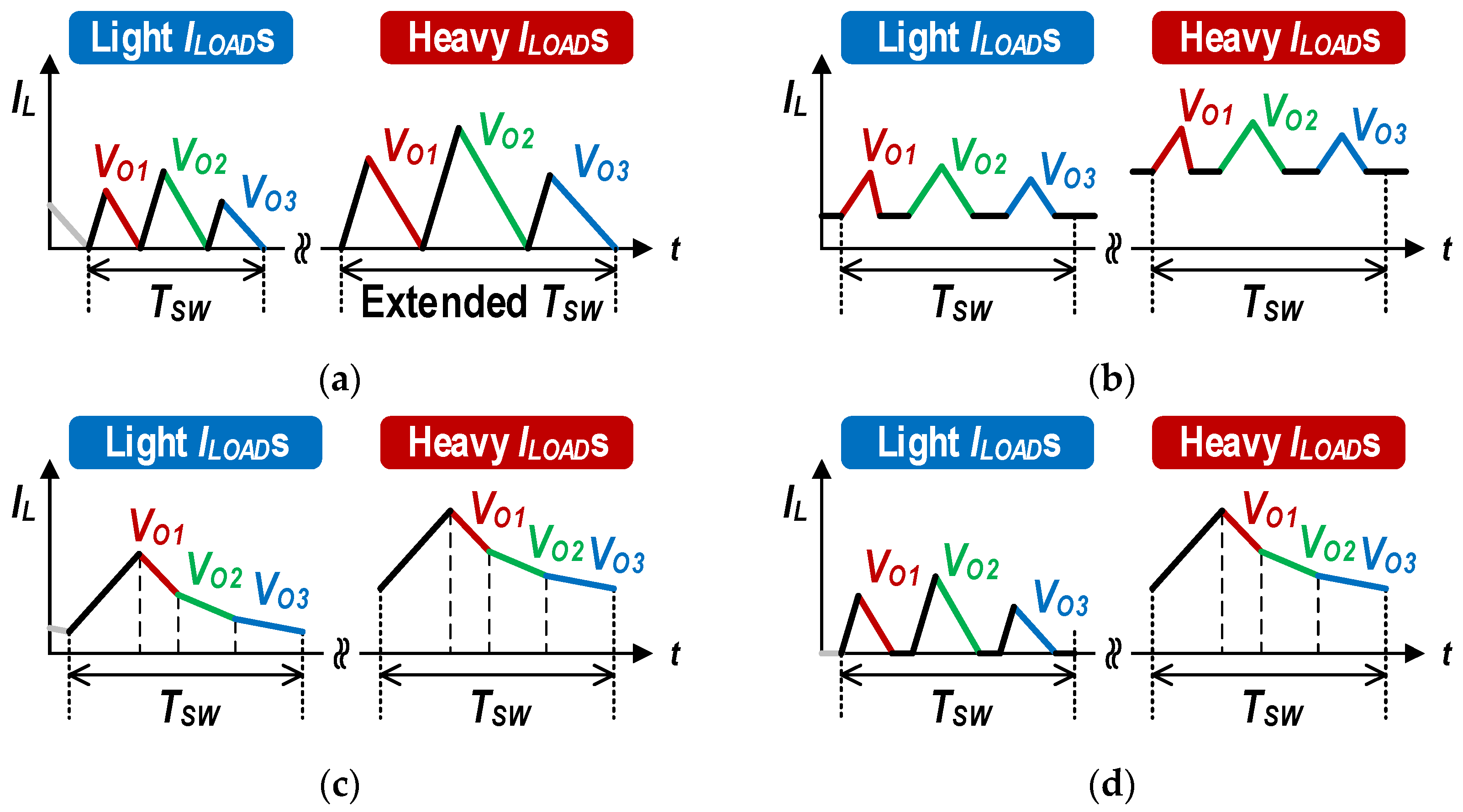
Figure 1 shows the charging operations of the conventional buck-based SIMO DC–DC converters. The inductor of the buck-based SIMO converters is always connected to the outputs for a switching cycle, and therefore, the power conversion efficiency (PCE) is improved due to lower peak
IL level and smaller output ripple. However, the voltage-second balance depends on each
VOUT level, and it causes a more complex switching control algorithm to suppress cross regulation when compared to the boost-based ones.
In parallel with these efforts, hybrid DC–DC converters have attracted increasing attention in power management ICs. They can achieve high PCEs even with small inductors that have a large DC resistance (DCR). To reduce the conduction loss caused by the inductor DCR, many approaches have been presented so far by lowering the rms inductor current (
IL) including the dual-path current topologies [
13,
14,
15,
16,
17] and switched-inductor-capacitor topologies [
14,
18,
19,
20,
21].
Recently, numerous efforts have exploited the advantages of hybrid structures in SIMO applications [
22,
23,
24,
25,
26,
27,
28,
29,
30,
31]. The SIMO hybrid DC–DC converter in [
24] was designed based on the switched-inductor-capacitor topology in [
16], achieving a peak efficiency of 87.5%. However, it requires six switched-capacitor power stages, consisting of eight switches and two flying capacitors (
CFs) each.
The SIMO hybrid 5-level converter in [
25] has an output power level that is limited to approximately 40 mW because it operates only in a discontinuous conduction mode. Moreover, when considering the
VIN range (<4.2 V), the output voltage (
VOUT) range was still narrow (0.4 to 0.9 V). The SIMO 3-level converter in [
26] had limited
VOUT controllability. Its first output (
VO1) is tunable, but it can only be regulated from 1/3× to 1/2× of
VIN. The other two
VOUTs are only regulated at 2× and 3×
VO1 in this system.
The most recent multi-input SIMO hybrid DC–DC converter was presented in 2022 [
31]. Using a single inductor, it manages two
VINs from transducers and three different
VOUTs.
However, because it is designed for applications of low-power sensor nodes, it operates in a discontinuous conduction mode to avoid the issue of the volt-second rule.
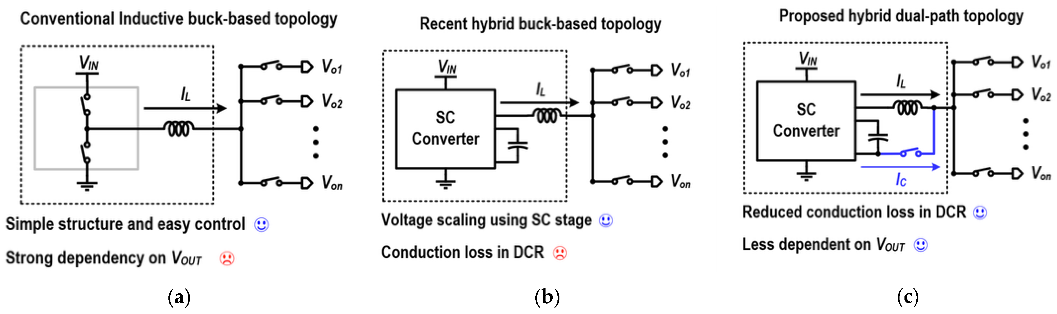
Figure 2 compares the conventional topology, a recently reported topology, and the proposed topology.
Figure 2a illustrates a buck-based SIMO converter using a single inductor,
Figure 2b shows a hybrid SIMO converter employing a flying capacitor, and
Figure 2c presents the proposed hybrid SIMO converter that forms a dual-current path using flying capacitors.
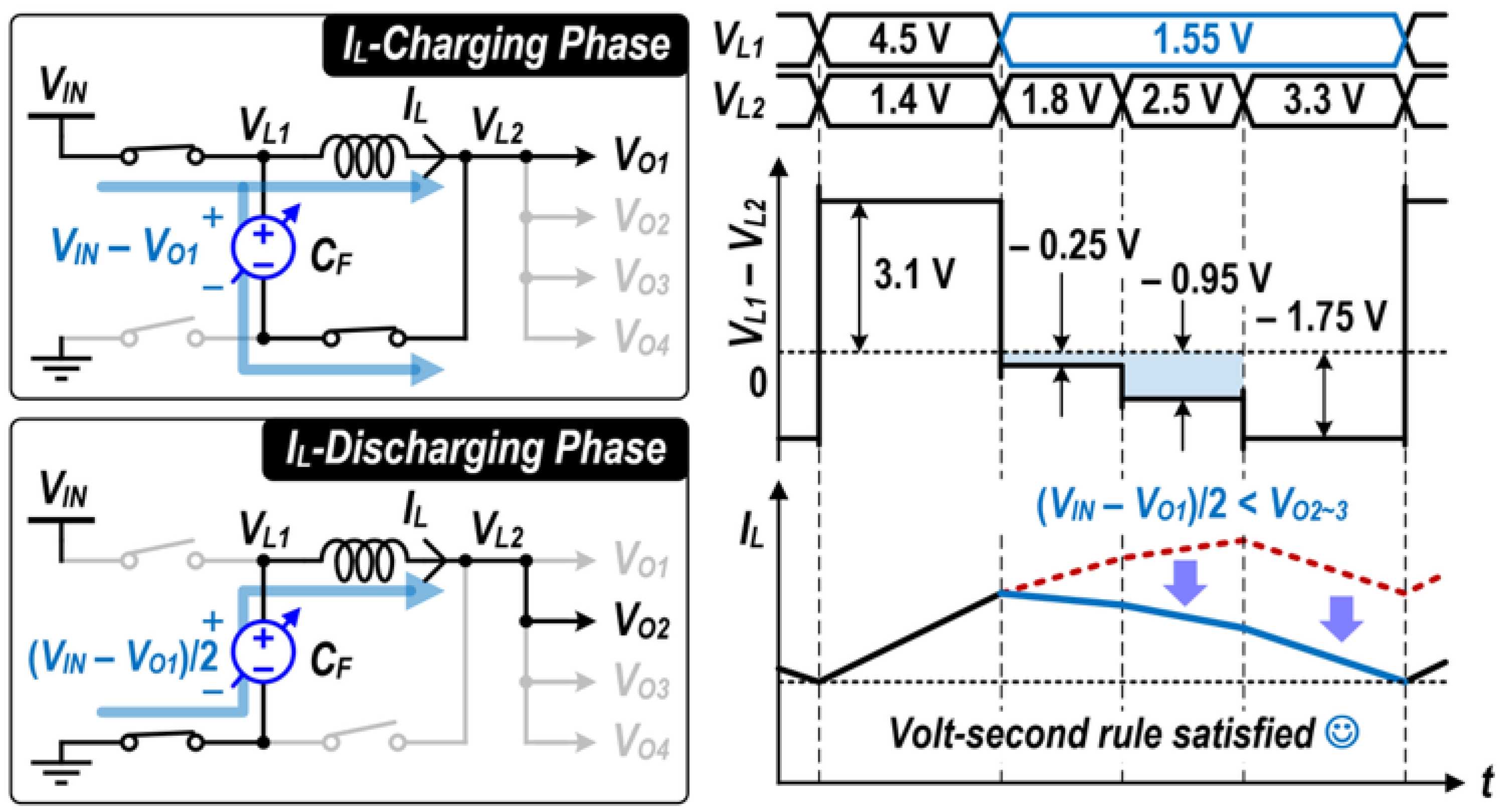
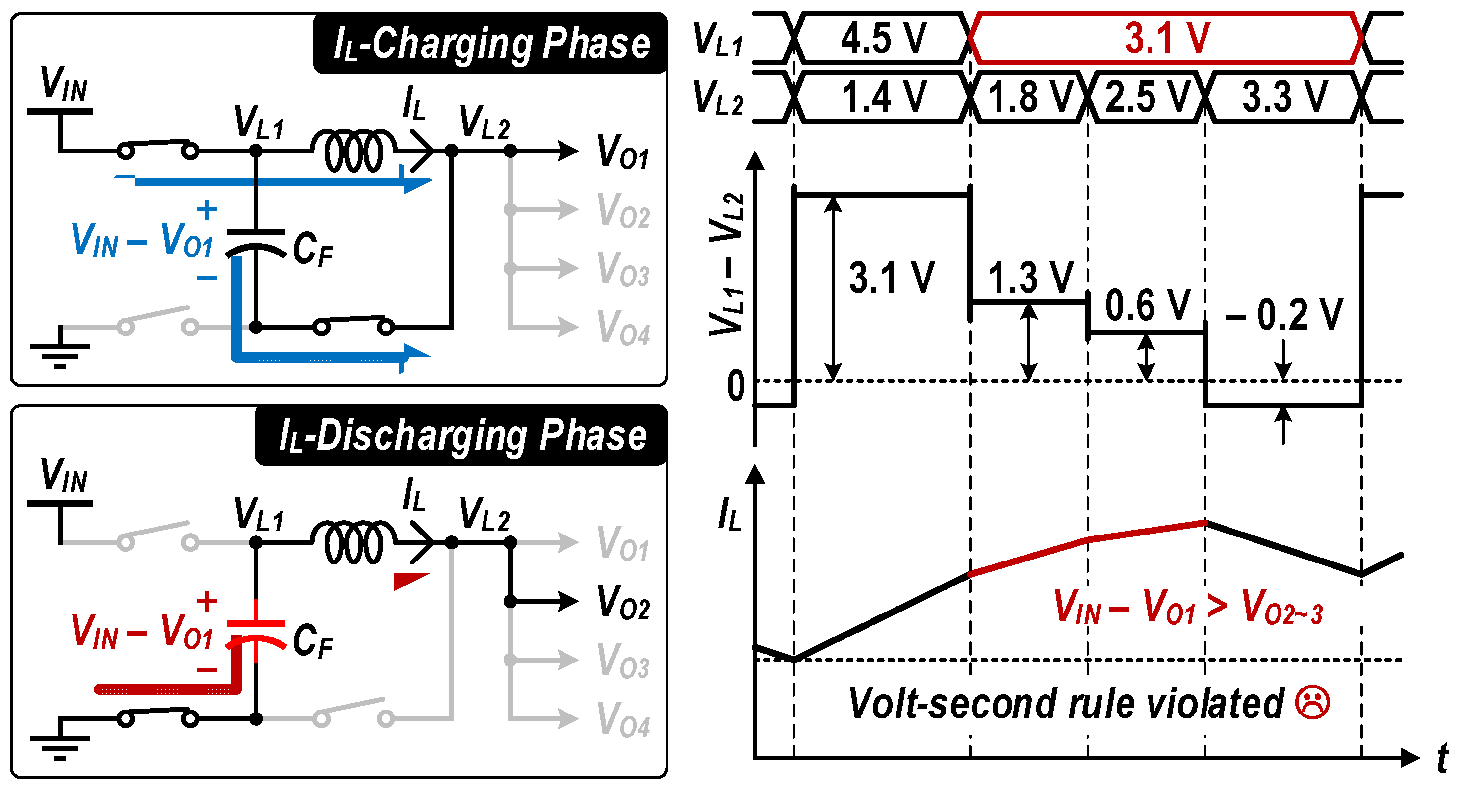
Figure 3 illustrates the violation of the volt-second balance when the dual-path hybrid topology is applied to multi-output applications.
CF is charged by (
VIN –
VO1) during the
IL-charging phase with 1.4 V of
VO1 and 4.5 V of
VIN. After this phase,
IL should be discharged with
VOUT lower than the switching node (
VL1). However, because
VL1 is formed at a higher voltage than other
VOUT levels (
VO2~4), the desired voltage across the inductor for discharging
IL cannot be obtained. Otherwise, to satisfy the volt-second balance condition, power should be delivered with limited
VOUT levels or a fixed output sequence.
To address this issue, the proposed topology adjusts the voltage across
CF (
VCF) according to the phase. As shown in
Figure 4, the proposed topology charges
CF to (
VIN –
VO1), similar to the prior work in the
IL-charging phase. In the
IL-discharging phase,
VL1 is lowered with capacitive voltage division, and a negative inductor current slope is obtained for different
VOUT levels to meet the volt-second balance.
To analyze this theoretically, the volt-second balance can be expressed as Equation (1), where
denotes the end time of the connection interval for each
VOUT, and
T represents one switching period. In addition,
,
,
, and
denote the output voltages sequentially connected from the first to the last within a single switching period. In this case, the worst-case condition occurs when the output with the lowest voltage is connected to the inductor during the inductor charging interval from 0 to
t1. Assuming
VIN = 4.5 V,
= 1.4 V,
= 1.8 V,
= 2.5 V, and
= 3.3 V, Equation (2) can be derived. Here, ∆t
1, ∆t
2, ∆t
3, and ∆t
4 represent the duty ratios of each phase within one switching period. Since the sum of all duty ratios within a single switching period is equal to unity, it can be expressed as Equation (3).
In addition, to ensure stable circuit operation, a minimum duty ratio of 0.1 is imposed as a design constraint. This condition can be expressed as Equation (4). Although the duty ratios can theoretically be obtained from the solution that satisfies Equations (2)–(4), it can be observed that no feasible solution exists. Even when the minimum duty ratio of 0.1 is assigned to Δt1, which corresponds to the largest voltage difference across the inductor, the required value of Δt4 exceeds unity. This indicates that the three equations cannot be satisfied simultaneously under this condition. Therefore, it can be concluded that the conventional dual-path topology may fail to satisfy the volt-second balance condition under certain operating conditions.
However, when the proposed work is analyzed under the same worst-case assumption, the resulting relationship can be derived as shown in Equation (5). A comparison between Equation (4) for the conventional method and Equation (5) for the proposed method shows that the voltage at the node preceding the inductor is reduced by half in the proposed configuration. This relaxation enables the existence of infinitely many feasible solutions. Each solution corresponds to a set of duty ratios, and since the required charge for each output determines the corresponding duty ratio, multiple duty combinations can satisfy the derived relationship.
This paper presents a SIMO hybrid buck converter that achieves
VOUTs over a wide range, and its PCE is improved by always applying a dual-path current to the heaviest-load output, regardless of the order in which
VOUTs are connected to the inductor during a cycle. The remainder of the paper is organized as follows.
Section 2 describes the circuit implementation and operation of the proposed system.
Section 3 presents the measurement results of the prototype chip. Finally, the conclusions are presented in
Section 4.
2. Proposed SIMO Hybrid Buck Converter
2.1. Circuit Implementation
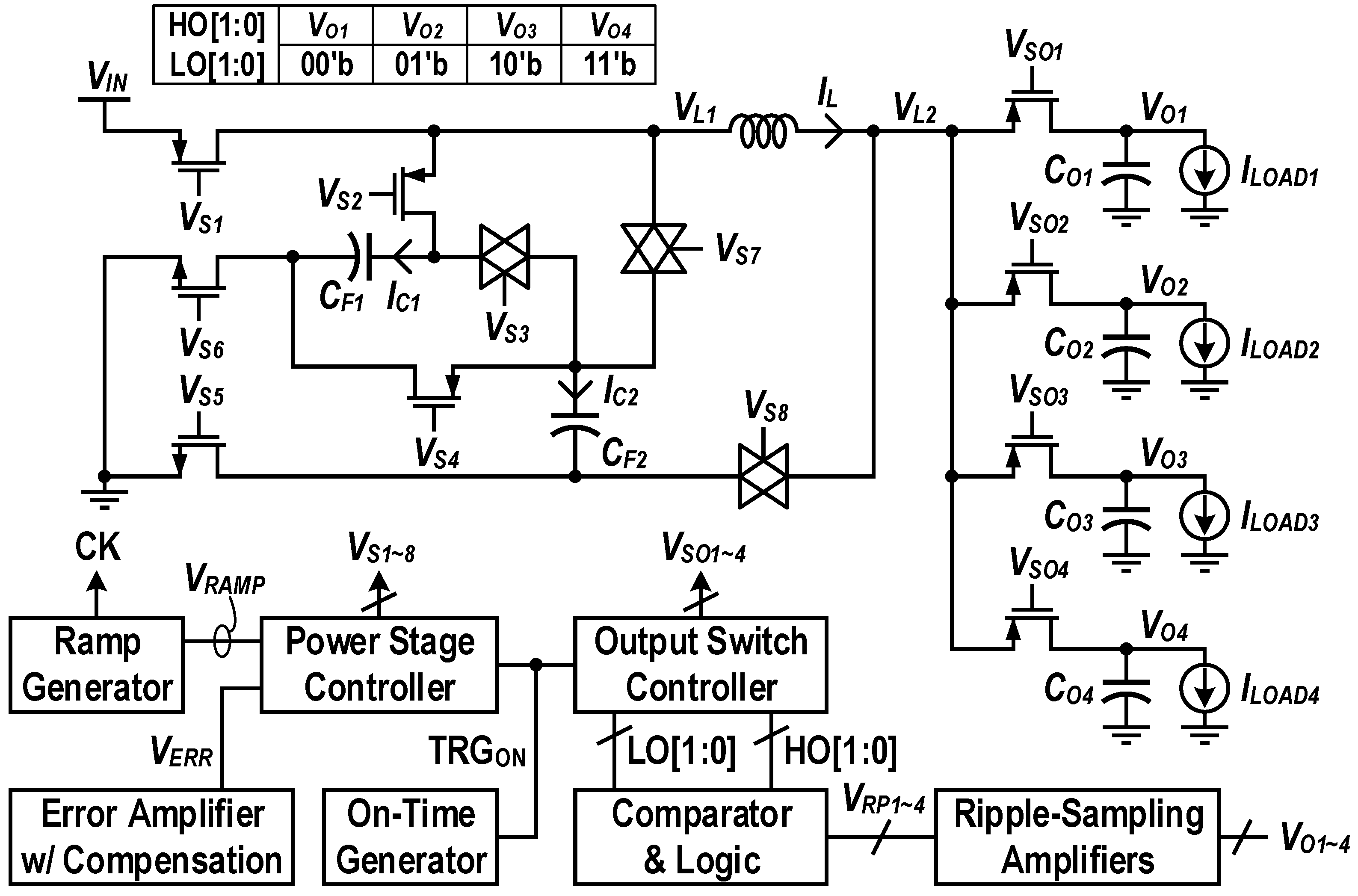
Figure 5 shows the top block diagram of the proposed SIMO hybrid buck converter. It comprises a power stage, output switches, and controllers. The duty cycle of the power stage is controlled by comparing the ramp signal (
VRAMP) with the error amplifier’s output signal (
VERR). The output switches are controlled by comparators and ripple samplers. The ripple-sampling amplifiers sample each
VOUT ripple to determine the sequence of the output switches. The two 2-bit digital signals, HO[1:0] and LO[1:0], indicate the heaviest- and lightest-load outputs, respectively, based on the ripple of each output. Using these digital signals, the output switch controller determines the order in which the output switches are turned on.
2.2. Switching Operation of Proposed Power Stage
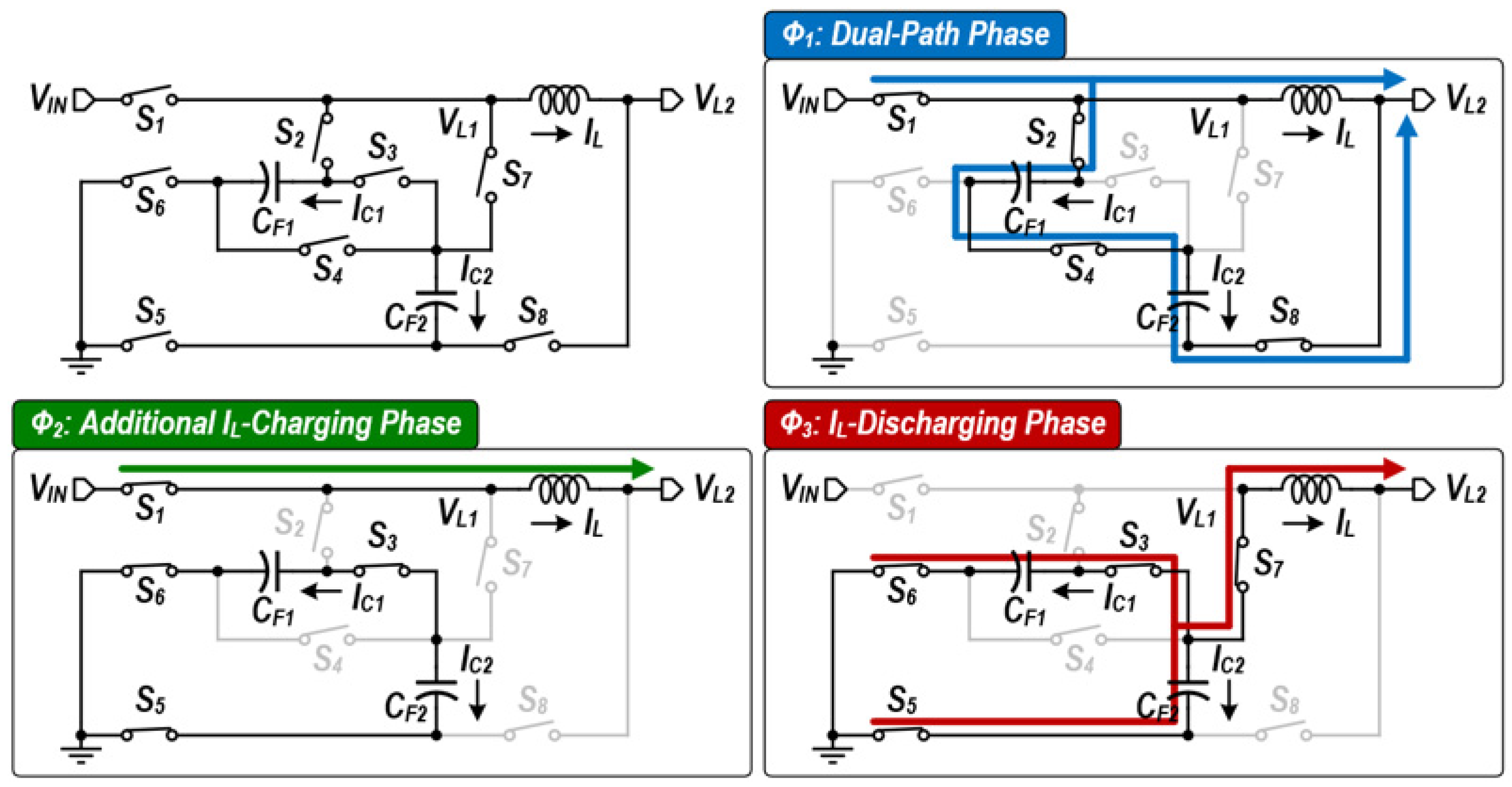
Figure 6 shows the proposed power stage of the SIMO hybrid buck converter and its switching operation. The power stage comprises eight power switches, two
CFs, and one inductor. Switches from S
3 to S
6 and two
CFs form a 2-to-1 converter structure, which replaces
CF of the prior single-output dual-path topology [
13]. In the dual-path phase (Φ
1),
VIN is applied to
VL1, and the output-switching node (
VL2) is connected to
VOUT with the heaviest load current (
ILOAD). Two
CFs are connected in series from
VL1 to
VL2 so that the dual-current path is formed, and the capacitor current (
IC) flows to the heaviest-load output. Because
IC and
IL flow simultaneously to the output, it is possible to supply a heavy
ILOAD even with a relatively low rms
IL and reduce the conduction loss due to DCR.
The second phase (Φ2) charges more IL when the IL charging of Φ1 is insufficient to drive the total ILOAD. In this phase, the switch of S7 is turned off, and only IL flows to the output. Because VL1 is connected to VIN, which is the highest voltage level in the system, IL is energized regardless of the VOUT level connected to VL2. During Φ2, two CFs, each charged to (VIN – VOn)/2, are connected in parallel. During the last phase (Φ3), IL is discharged by connecting VL1 to the top plates of CFs. Because VL1 is halved compared to the conventional work, discharging IL is possible over a wider range of VOUT levels.
The case in which the conduction loss can be reduced the most by the dual-path current is when
VOUT with the heaviest
ILOAD is supplied by the dual-path current in Φ
1 to reduce the rms value of
IL levels. However, each
ILOAD of the four
VOUTs is situational. Therefore, the proposed work utilizes the load-dependent sequencing technique, where the heaviest-
ILOAD output is always connected to the inductor first to lower the conduction loss by the dual-path current. In the worst case of the conventional topology [
13], where
ILOAD of the lowest
VOUT level is the heaviest,
IL charges only for one cycle.
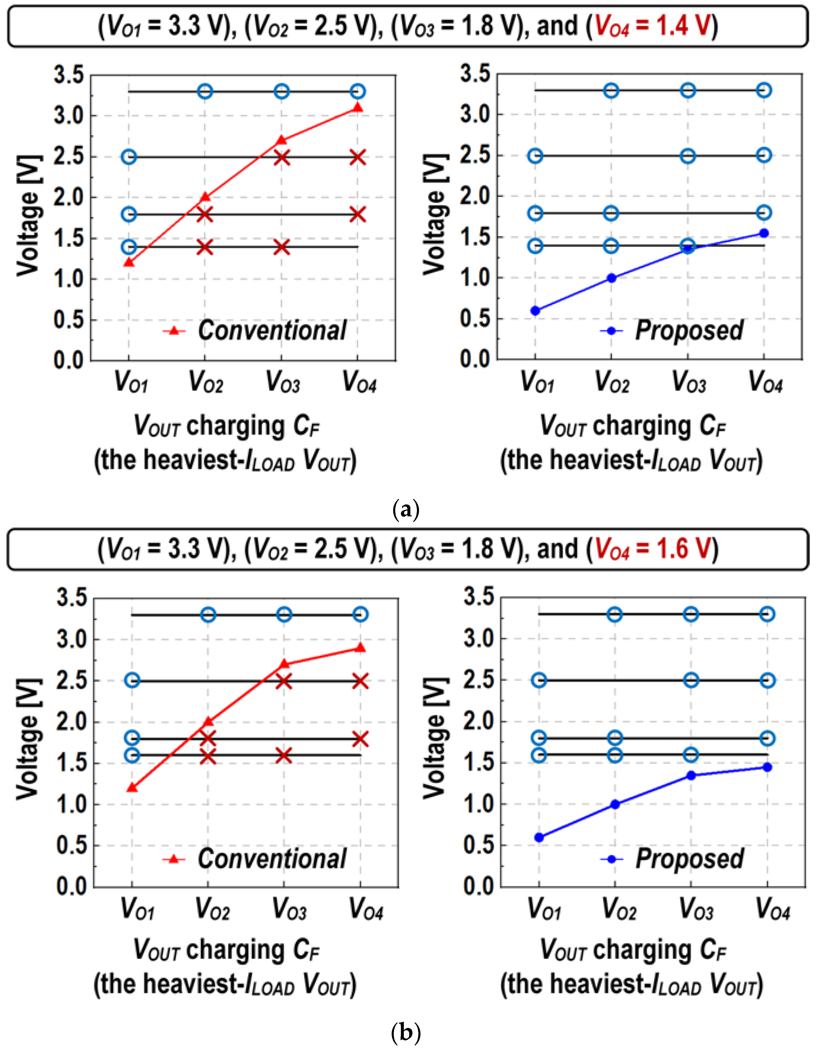
Figure 7 compares the number of output cases in which
IL can be discharged depending on the voltage charged to
CF for the conventional and proposed topologies. As aforementioned, when the heaviest-load
VOUT of
VOn is connected to
CF for the dual-path current in the conventional work,
CF is charged to (
VIN –
VOn). To discharge
IL, (
VIN –
VOn) should be lower than other
VOUTs. However, as shown in
Figure 7a, when the lowest-voltage output of
VO4 is regulated at 1.4 V, the prior topology, which utilizes the load-dependent sequencing technique where
VOUT with the largest
ILOAD charges
CF, cannot discharge
IL in all cases. As shown in
Figure 7b, higher voltage
VO4 releases the constraint, but there are still cases where
IL cannot be discharged in the conventional topology. This means that the prior work must have a switching sequence dependent on
VOUT levels to satisfy the volt-second rule, or it cannot regulate multi
VOUT rails.
However, as shown in
Figure 7a,b, the proposed topology halves the voltage of (
VIN –
VOn) by using two
CFs, and since it always has a voltage level lower than the remaining
VOUTs, discharging
IL is possible for all switching sequences. Therefore, the proposed topology satisfies the volt-second rule in all cases, regardless of the
ILOAD level and switching sequence.
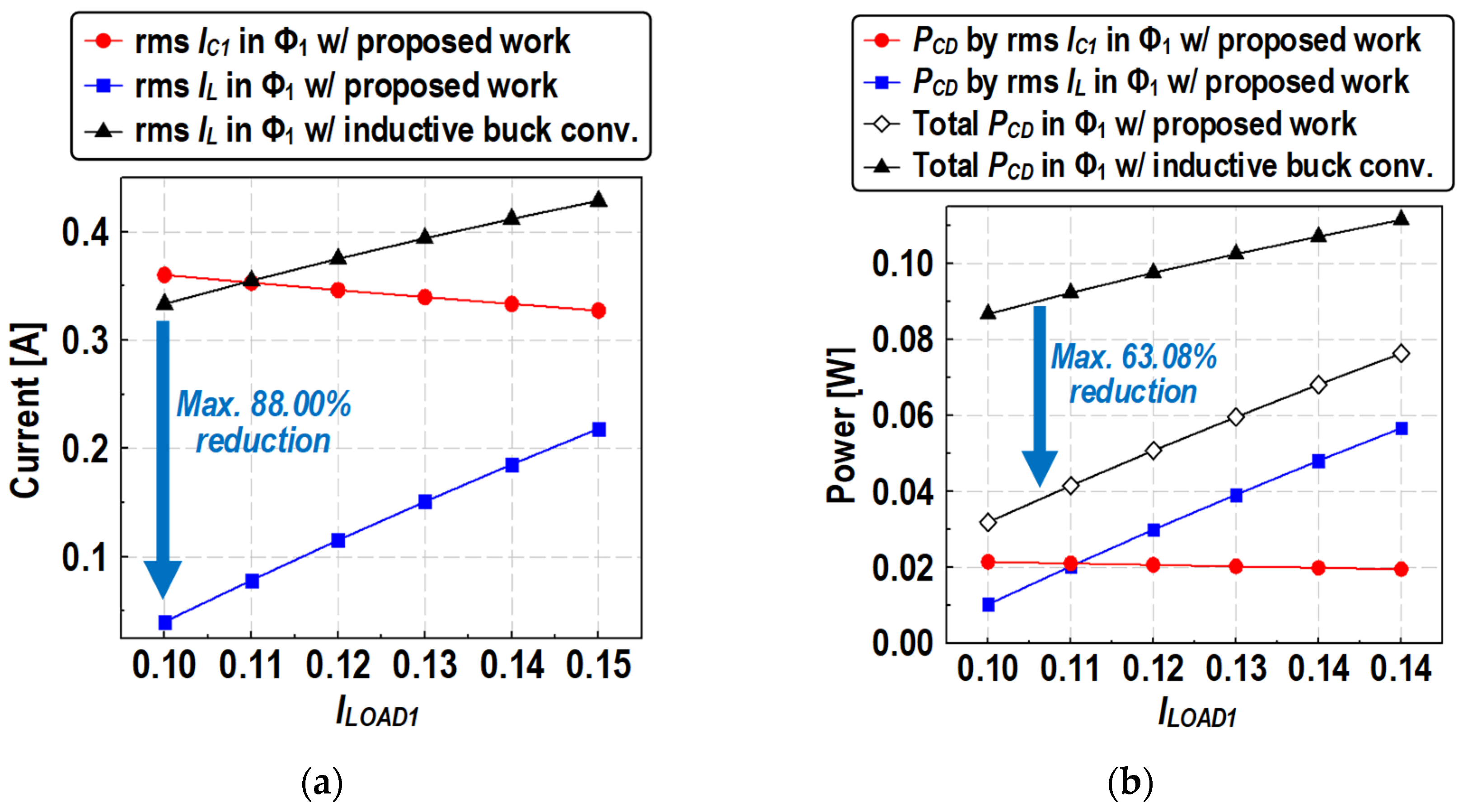
Figure 8 compares the rms current levels and conduction loss in Φ
1 based on the analysis.
ILOAD1 was assumed to be the heaviest at 100 mA.
ILOAD2,
ILOAD3, and
ILOAD4 were assumed to be 80, 60, and 40 mA, respectively. As shown in
Figure 8a, the rms
IL in Φ
1 of the proposed topology was reduced by approximately 67% on average compared to the inductive buck topology due to the dual-path current. However, there were four power switches and two
CFs, raising concerns regarding increased conduction loss.
Figure 8b compares the total conduction loss in Φ
1. In this analysis, it was assumed that the on-resistance of the power switches and the equivalent series resistance (ESR) of
CFs was 10 mΩ and the inductor DCR was 250 mΩ. The on-resistance value was estimated from simulation results, while the ESR of
CFs and DCR of the inductor were obtained from the corresponding component datasheets. Although
IC flowed through six resistive components, the conduction loss in Φ
1 was reduced by 45.9% on average because the conduction loss due to DCR was dominant.
2.3. Mode Control of Proposed Power Stage
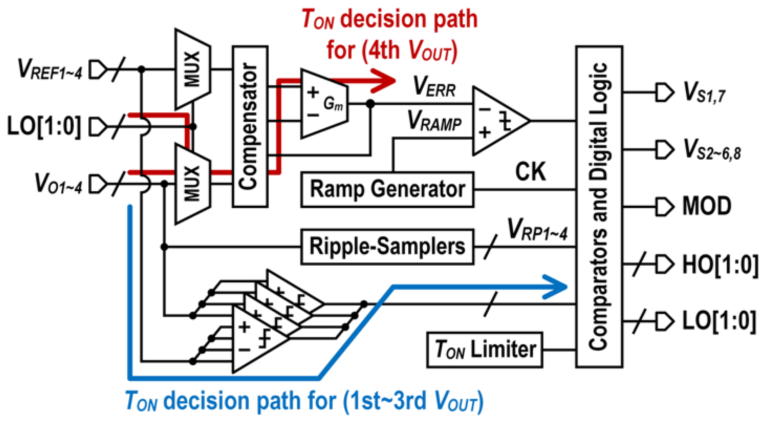
Figure 9 shows the block diagram of the on-time (
TON) controller. The target
VOUT levels were 3.3, 2.5, 1.8, and 1.4 V.
TONs of the first to third
VOUTs are determined by hysteresis comparators, and the error amplifier determines the overall
TON based on the error of the last output. To determine the switching sequence of the output switches, the output with the heaviest and lightest
ILOADs must be identified, and
ILOAD of each output can be compared based on the output ripple during the certain time. Therefore, four ripple samplers sense the ripple of each output, and the comparator and digital logic generate two 2-bit signals (HO[1:0] and LO[1:0], respectively) identifying the outputs with the heaviest and lightest
ILOAD, based on the sampler outputs (
VRP1~4).
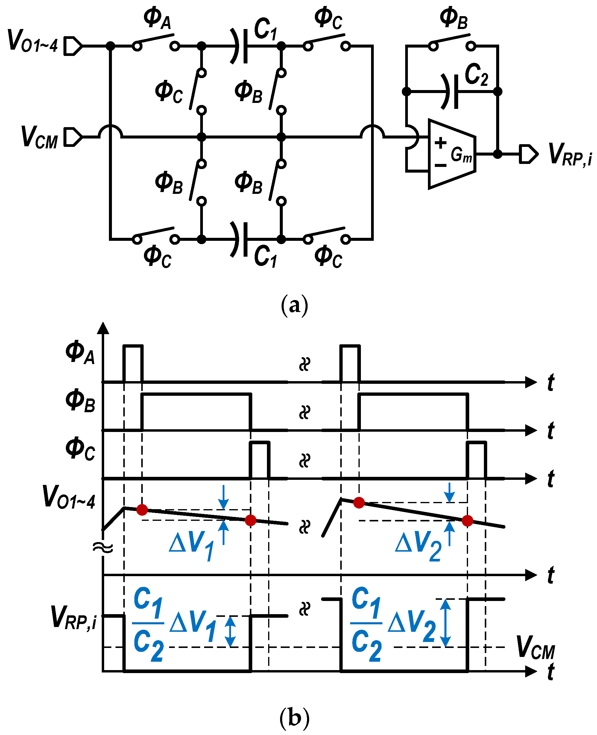
Figure 10 shows the schematic and operation of the ripple sampler. As shown in
Figure 10a, it is implemented as a switched-capacitor type to cover the wide input common mode range and match the output common mode. As shown in
Figure 10b, each
VOUT ripple is sampled and amplified for the same period after charge transfer from the power stage is complete. The gain of the amplifier is calculated as
C1/
C2, and was designed to be three in the proposed work. The turn-on sequence of the output switches is determined by comparing
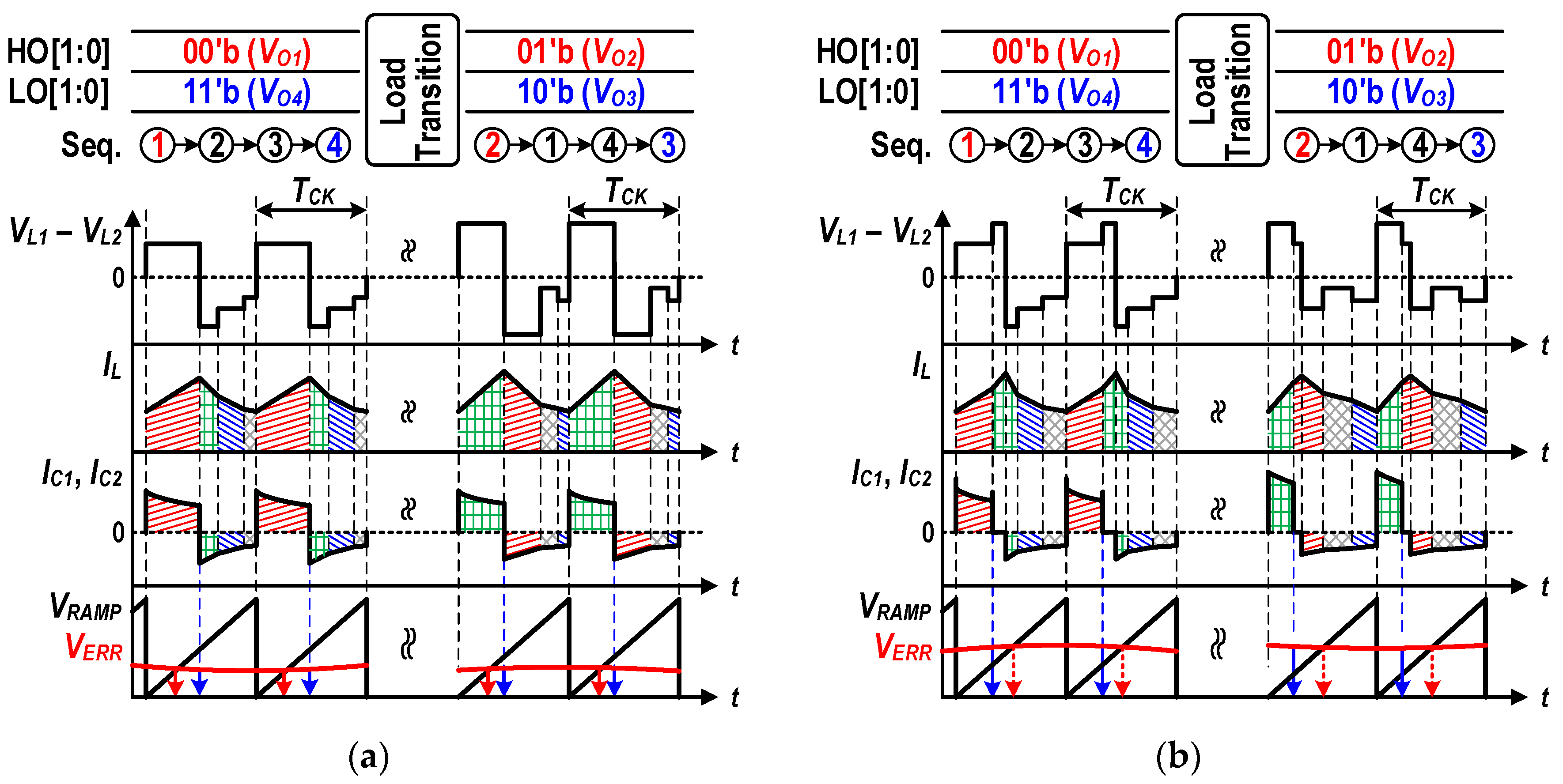
VRPi. Figure 11 shows the operating waveforms of the proposed power stage. The two-phase mode comprises Φ
1 and Φ
3, whereas the three-phase mode has an additional Φ
2 between them to increase
IL further. As aforementioned, the rms
IL level reduction based on the dual-path topology is the most effective when the dual-path current is supplied to the heaviest-
ILOAD output. To analyze this technique mathematically, during Φ
1, both
IL and
IC flow to the output. To ensure charge balance of the flying capacitor, the current delivered through the flying capacitor during the inductor charging interval must be equal to that during the discharging interval. Therefore, the condition in Equation (6) must be satisfied. In addition, the volt-second balance condition must also be satisfied. Therefore, Equation (7) can be derived. From Equations (6) and (7), it can be observed that the average value of
IL during Φ
1 is equal to that of
IC. This result implies that only half of the load current flows through the inductor during Φ
1. Based on this relationship, the power loss caused by the inductor DCR during Φ
1 can be expressed as Equation (8), where
ILOAD1st denotes the load current of the first-connected output.
In contrast, during Φ3, when the inductor is discharging, the load current of the output connected to the inductor flows through the inductor. As a result, there is a limitation in reducing the conduction loss caused by the inductor DCR during this interval. Therefore, the conduction loss associated with the inductor DCR over one switching period can be minimized when the output with the largest load current is connected to the inductor first and supplied through the dual-path.
Therefore, the load-dependent sequencing technique is proposed, and it changes the output switch sequence according to the
ILOAD level. The sequence of the output switches is determined by HO[1:0] and LO[1:0]. As shown in
Figure 11, the heaviest- and lightest-
ILOAD outputs receive the charge first and last, respectively. For the other two outputs, the output with a higher
VOUT is first connected to the inductor.
The operating mode is determined by comparing the intersection point of VERR and VRAMP with the turn-off point of the output switch for the heaviest-load output. VERR is adjusted by the lightest-load VOUT according to LO[1:0]. When the first output switch is turned off later than the intersection point, the power stage operates in the two-phase mode to lower the IL level. Otherwise, if VERR crosses the rising VRAMP after the first output switch is turned off, the power stage operates in the three-phase mode. Therefore, with the proposed two- and three-phase modes, the total load charge matches the total charge delivered to the outputs.
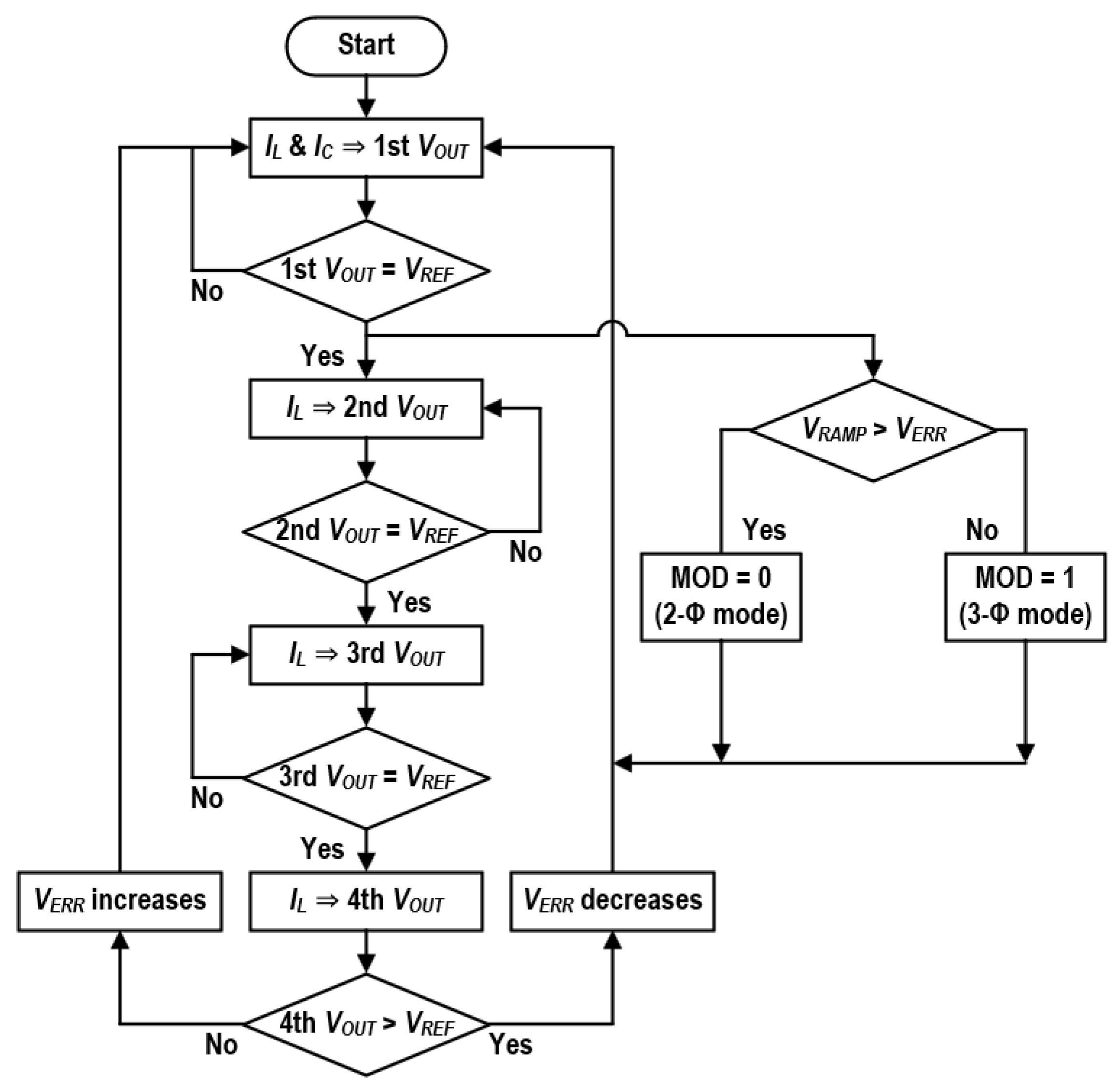
The overall control operation of the proposed controller is illustrated as a flowchart in
Figure 12. The controller continuously monitors the output voltages through ripple-sampling amplifiers and determines the regulation priority among the outputs. Based on the sampled ripple information, the digital control logic selects the corresponding output channel through a multiplexer and generates the appropriate
TON decision path. In this process, the error amplifier produces the control voltage (
VERR), which is compared with the ramp signal (
VRAMP) to determine the on-time of the power stage. This ramp-comparator-based mechanism allows the controller to regulate the output voltages while allocating the inductor energy to the selected output in a time-multiplexed manner. Through this procedure, the controller sequentially evaluates the regulation condition of each output and updates the switching decision accordingly.
During the transition between two-phase and three-phase operation, the controller reconfigures the switching sequence according to the selected operating mode. The digital logic block updates the TON decision path and the corresponding switch control signals while maintaining the same voltage regulation loop. Since the fundamental voltage-mode control loop remains unchanged and only the output selection sequence is modified, stable regulation can be maintained during the mode transition. Therefore, the proposed control flow ensures reliable output regulation and smooth operation of the power stage even when the operating mode changes.
2.4. Transfer Function Analysis
The proposed converter generates four regulated output voltages using a single inductor and a flying capacitor network. However, deriving a complete dynamic model for the four-output system significantly increases the modeling complexity of the state-space representation due to the increased number of state variables and switching states. To simplify the analytical derivation while preserving the fundamental energy transfer mechanism of the converter, the system is reduced to an equivalent two-output model for the analytical modeling.
To gain analytical insight into the impact of duty redistribution caused by the load-dependent sequencing, a simplified equivalent model considering two representative outputs was adopted. Based on this model, the control-to-output transfer functions were derived and analyzed. The analysis shows that the redistribution of the effective duty ratios alters the dynamic characteristics of the output regulation, which can degrade the cross-regulation performance. Although the analysis was derived from the simplified model, the same operating mechanism exists in the proposed multi-output converter, leading to similar behavior in the measured results. In this simplified representation,
V1 denotes the first connected output voltage and
V2 represents the subsequent output stage. Since the proposed converter sequentially delivers energy to multiple outputs through the flying capacitor network, the two-output model sufficiently captures the essential dynamic characteristics of the overall system. For the modeling analysis, the converter was assumed to operate in continuous conduction mode, and the flying capacitors were assumed to be sufficiently large so that their voltage ripple could be neglected. Under steady-state conditions, the voltages across the two flying capacitors become identical due to the symmetric structure of the flying capacitor network. Therefore, the voltages across the flying capacitors can be expressed as Equation (9). The converter operates in two switching states within one switching period, determined by the duty ratio (D).
During Φ
1, the inductor is connected to the flying capacitor network and delivers energy to the first output stage. The voltage applied to the inductor is
VIN –
V1. Thus, the inductor current variation is given by
During Φ
2, the inductor is connected to the second output node
V2. Therefore, the current flowing through the output capacitor
C2 is
where
R2 is
V2/
ILOAD2. During Φ
2, the inductor is connected to the second output stage and transfers energy to
V2. The voltage applied to the inductor becomes
From Equation (12), the inductor current variation is
In this state, the inductor current is delivered to the second output stage. Therefore, the current flowing through the capacitor
C2 is
To obtain the averaged large-signal model, the state equations are averaged over one switching period. The average inductor dynamic equation can be written as
and the capacitor voltage dynamic equation is obtained as
The large-signal averaged model is obtained as Equations (15) and (16). These equations describe the dynamic behavior of the inductor current and the second output voltage. To derive the control-to-output transfer function, the variables are decomposed into their steady-state values and small perturbations as iL = IL + , vO = VO + , and d = D + .
Substituting these into the averaged model and neglecting second-order perturbation terms yields the linearized small-signal model. After linearization, the small-signal equations become Equations (17) and (18).
From the aforementioned equations, the control-to-output transfer function, G
vd,2phase(s), of the converter for
V2 is finally derived as Equation (19).
The transfer function derived above represents the dynamic behavior of the proposed converter assuming two outputs under the two-phase operation. When the load current demand increases, the proposed converter operates in a three-phase mode to provide additional inductor charging. For analytical simplicity, the modeling is again performed assuming two output stages. In this case, the time interval during which the inductor is connected to V1 through the dual-path during the inductor charging period is defined as d1, the time interval during which the inductor is connected to V2 through a single path during the charging period is defined as d2, and the time interval during which the inductor discharges to V2 is defined as (1 − d1 − d2). Based on these assumptions, the corresponding transfer function can be derived as follows in Equation (20).
The resulting transfer function exhibits a form similar to that obtained under the two-phase operation. This is because d
2 is assumed to be constant in the derivation of the control-to-output transfer function
/
, which leads to a similar mathematical structure. In addition, since the output
V2 receives energy during the interval (1 − d
1), the dynamic behavior of
V2 is primarily determined by d
1, resulting in a transfer function that closely resembles the one derived for the two-phase operation.
On the other hand, if the transfer function / is derived, the presence of a direct energy transfer path from the inductor to V2 during the d2 interval may mitigate the right-half-plane zero. However, to provide a fair comparison with the conventional two-phase operation, the transfer function with respect to d1 was considered in this analysis. The derived transfer function was therefore used to analyze the dynamic characteristics of the proposed converter under heavy-load conditions.
3. Measurement Results
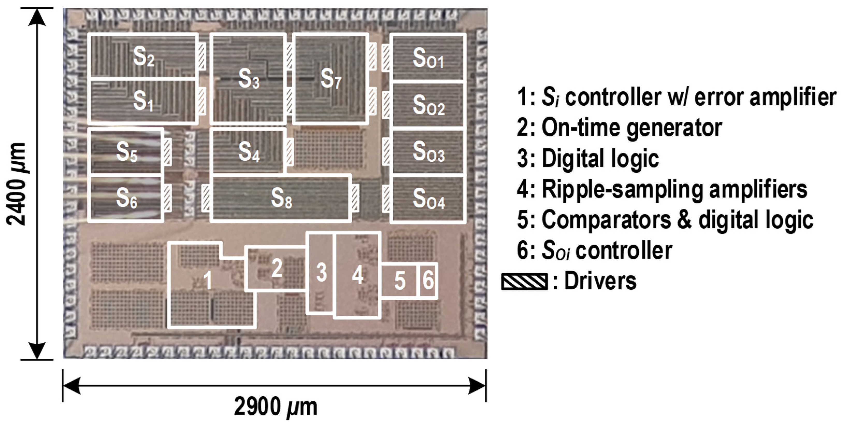
Figure 13 shows the chip micrograph. This was implemented in a 180-nm CMOS technology, and the chip area was 6.96 mm
2.
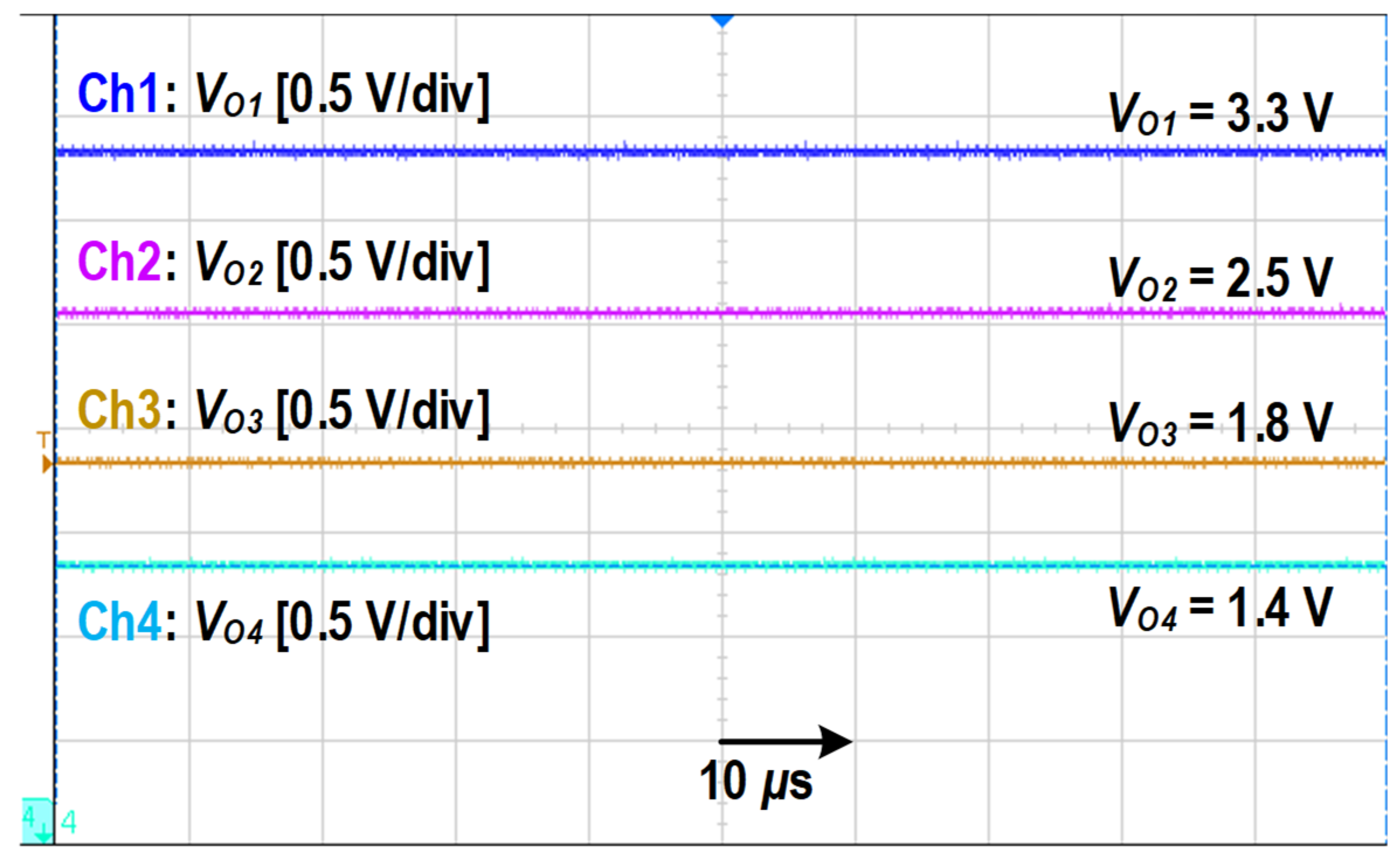
Figure 14 shows the steady-state waveforms of the proposed work. The waveforms were measured at
VIN = 4.5 V and a switching frequency of 1 MHz. A 4.7-μH inductor was used, and its DCR was 250 mΩ. Two 10-μF capacitors were used as
CFs. The four
VOUTs were regulated to 3.3, 2.5, 1.8, and 1.4 V according to HO[1:0] and LO[1:0].
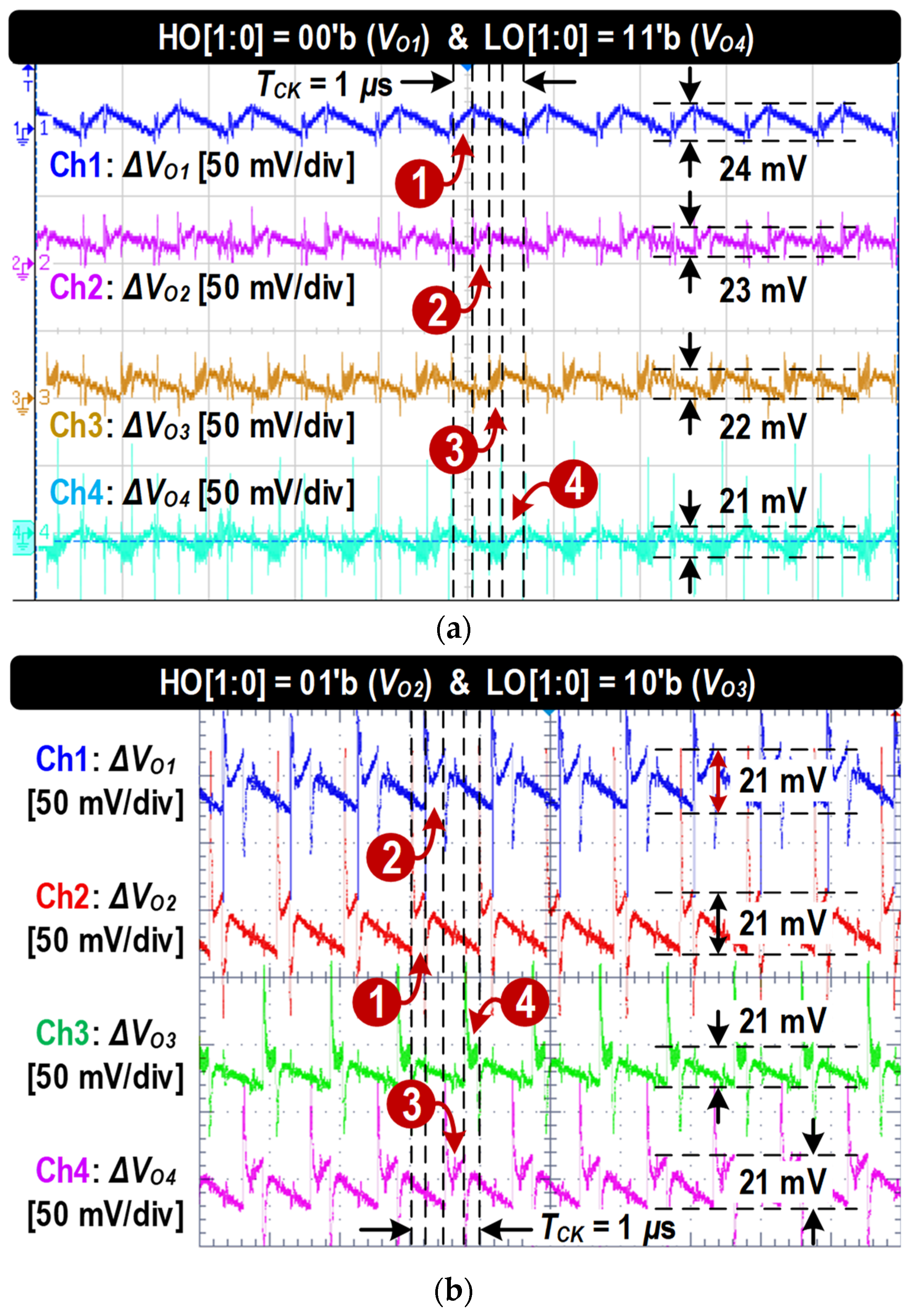
Figure 15 shows the voltage ripples of the proposed work. As aforementioned, the output switching sequence is determined by the relative
ILOAD levels. As shown in
Figure 15a,b, the heaviest-
ILOAD output is supplied first; subsequently, the two moderate-
ILOAD outputs are supplied in order according to their voltage levels; finally, the lightest-
ILOAD output is supplied last. With the
ILOAD range between 60 mA and 100 mA for each
VOUT, the
VOUT ripples were measured as from 20 mV to 24 mV neglecting high-frequency noise.
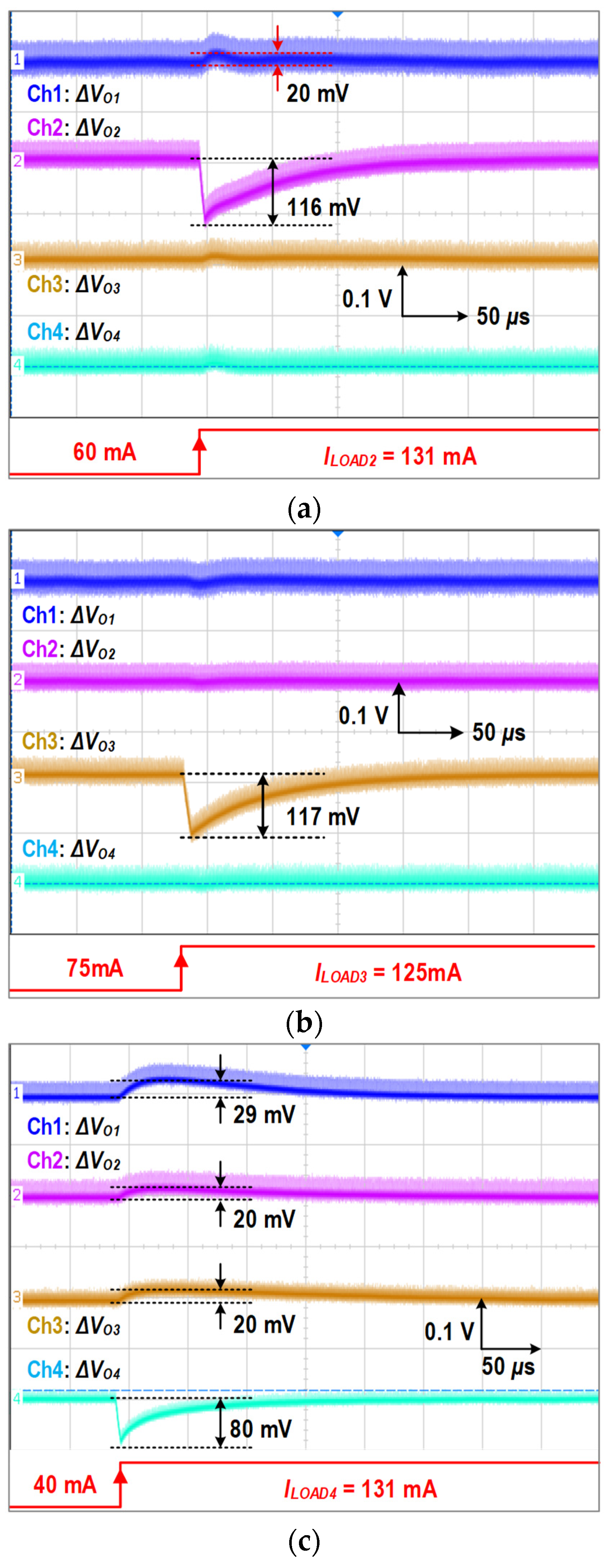
The load-transient responses are shown in
Figure 16. When
ILOAD2 changed from 60 mA to 131 mA for 600 ns; the overshoot and settling time were measured as 116 mV and approximately 100 μs, respectively. The cross regulation was measured as 0.29 mV/mA.
Figure 16b,c shows the measured load-transient responses of the third and fourth
VOUT, respectively. When
ILOAD3 changed from 75 mA to 125 mA, the overshoot and settling time were measured as 117 mV and approximately 115 μs, respectively. When
ILOAD4 changed from 40 mA to 131 mA over 600 ns, the undershoot at
VO4 and the settling time were measured to be 80 mV and 100 μs, respectively. The worst cross regulation of the proposed work was measured to be 0.31 mV/mA, which is larger than that of conventional SIMO buck converters. When
ILOAD varies sufficiently to reorder the sequencing of the output switches, the resulting changes in duty cycle and operating mode during the transient affect stability and cross-regulation.
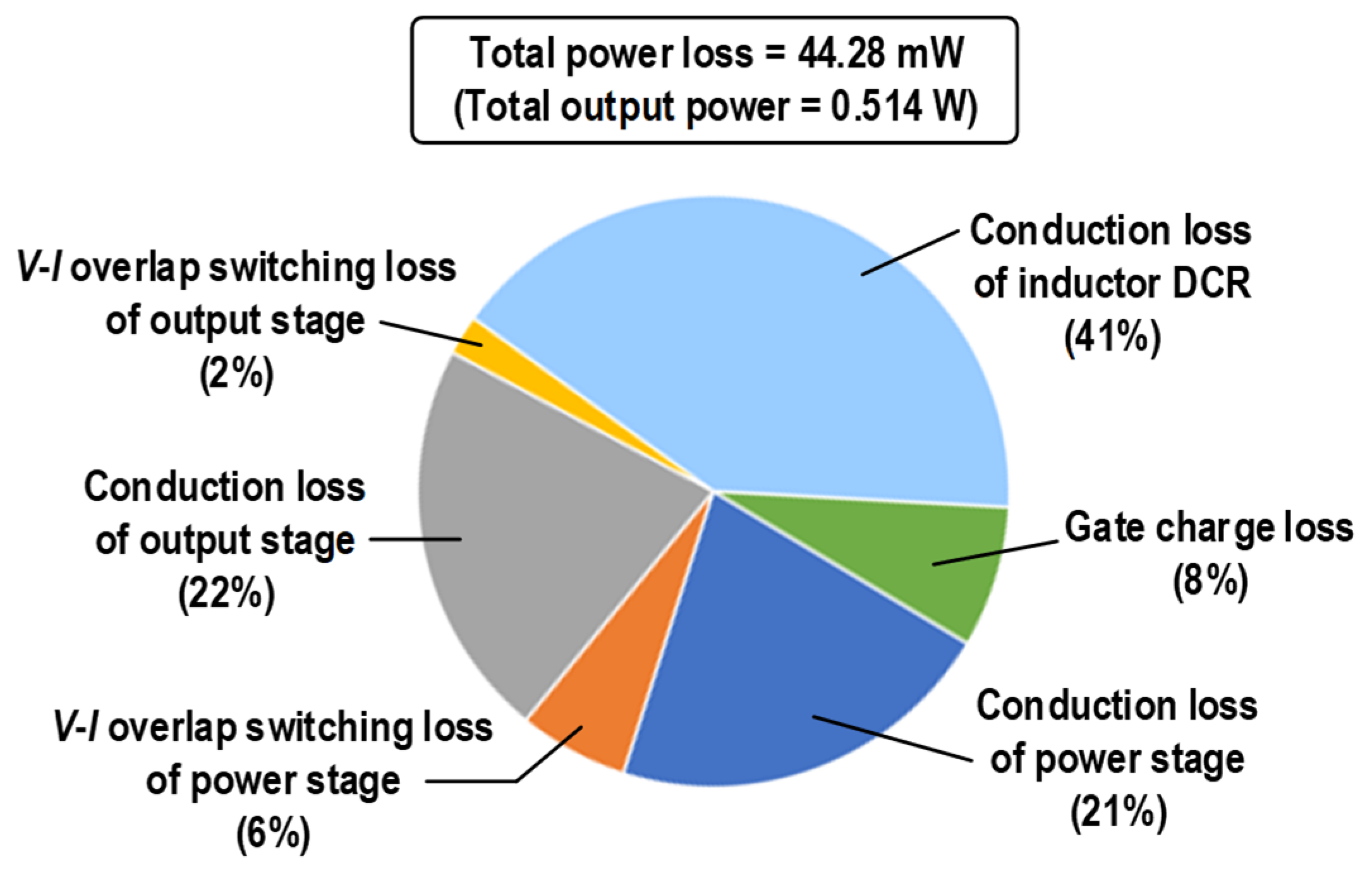
Figure 17 presents the loss breakdown when an inductor with a DCR of 250 mΩ is used. As shown in the pie chart, the conduction loss caused by the inductor DCR was the dominant loss component in hybrid DC–DC converters, and therefore had the greatest impact on the overall efficiency. In the proposed converter, the load-dependent sequencing strategy allows the output with the largest
ILOAD to be supplied through the dual-path operation, resulting in the inductor current being reduced to half of the load current. Consequently, the conduction loss caused by the inductor DCR is minimized, leading to an improvement in the overall efficiency.
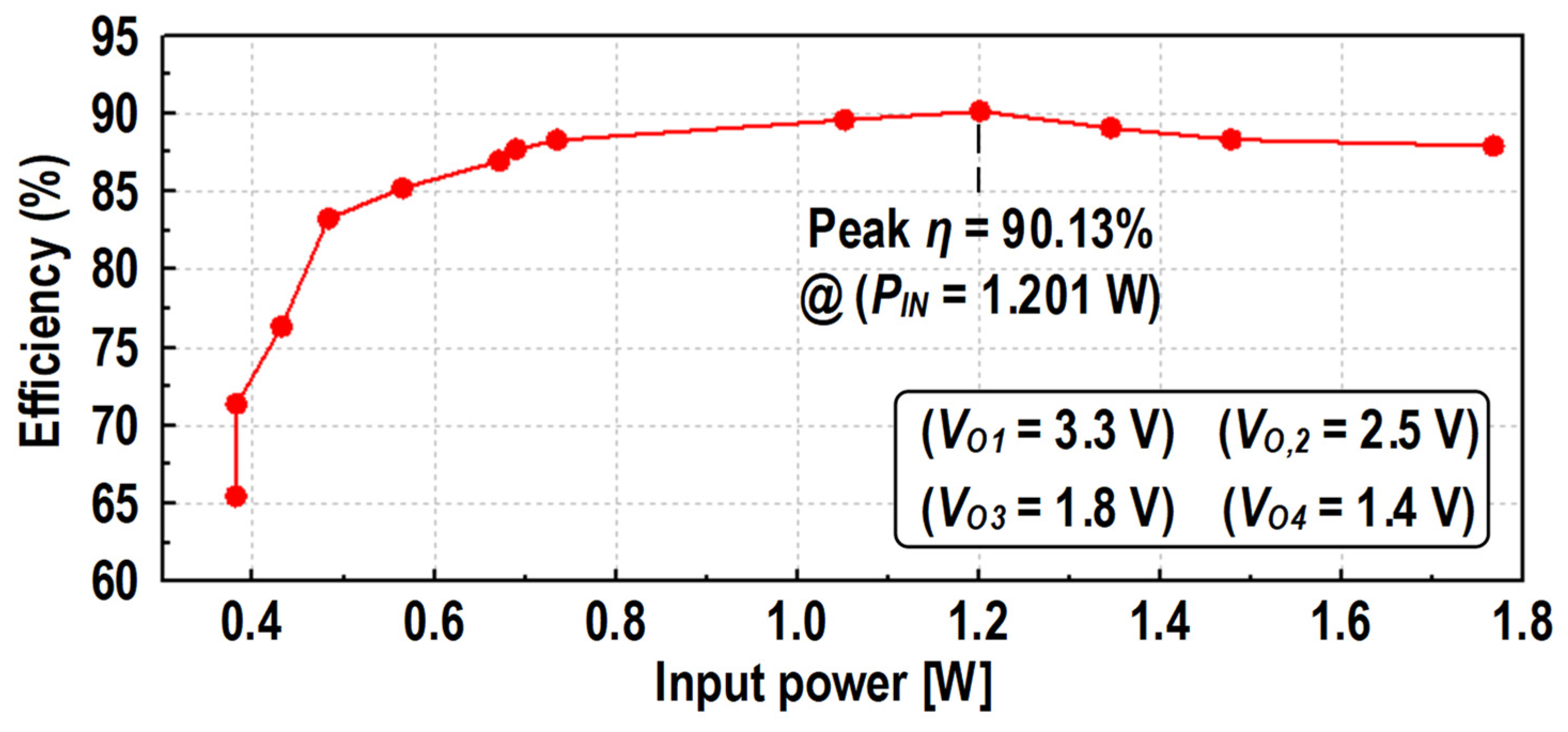
Figure 18 shows the measured total PCE, and the maximum PCE was measured as 90.13% with 1.20 W of the input power.
Table 1 shows a summarized performance of the proposed work compared to the prior SIMO hybrid converters. This work simultaneously regulated the four
VOUTs using the proposed SIMO hybrid buck converter. Although the DCR of the inductor was as high as 250 mΩ, the proposed work showed a peak PCE of 90.13% by utilizing the dual-path topology. Moreover, the proposed work achieved the widest
VOUT range from 1.4 to 3.3 V when compared to the prior SIMO hybrid buck converters.