1. Introduction
Neuromorphic computing has emerged as a compelling paradigm for next-generation information processing, driven by the demand for fast, energy-efficient, and scalable solutions to data-intensive artificial intelligence (AI) workloads. Conventional von Neumann architectures suffer from intrinsic processor–memory bottlenecks due to the physical separation of computation and storage, resulting in excessive data movement and energy dissipation. In contrast, neuromorphic systems emulate the distributed and parallel organization of biological neural networks, enabling efficient execution of learning and inference tasks with significantly reduced energy overhead [
1].
A defining feature of neuromorphic hardware is the use of artificial neurons and synapses that simultaneously store and process information. Learning occurs locally through synaptic adaptation, which minimizes global data transfer and enables event-driven computation [
2]. This paradigm places stringent requirements on circuit elements capable of retaining internal states without continuous power supply while exhibiting continuously tunable dynamics. Such elements provide adaptive, nonvolatile memory and processing capabilities, closely resembling biological learning mechanisms [
3].
At the circuit level, these requirements are naturally addressed by memory circuit elements, commonly referred to as memelements. Memelements extend classical circuit theory by introducing nonlinear, state-dependent constitutive relationships between fundamental electrical variables, thereby embedding memory directly into circuit behavior [
4]. Since their formal introduction, memelements have been extensively investigated for applications in nonvolatile memory, neuromorphic computing, adaptive signal processing, chaotic systems, and unconventional computing architectures [
5].
Among memelements, the memristor—originally postulated by Chua in 1971—has received the greatest attention due to its voltage–current formulation and relative ease of physical realization [
6]. This framework was later generalized to include memcapacitors and meminductors, further expanding the design space for nonlinear memory-enabled circuits [
4]. Beyond these widely studied elements, the memtranstor represents a distinct and comparatively less explored class of memelements, characterized by a constitutive relationship between electric charge and magnetic flux arising from magnetoelectric coupling.
Unlike memristors, which are governed by voltage–current dynamics, the memtranstor operates intrinsically in the flux–charge domain. Although it shares the same dimensional unit (ohms), the memtranstor is fundamentally different in both physical origin and mathematical description. This distinction leads to characteristic pinched hysteresis loops in the charge–flux plane, often exhibiting butterfly-shaped or slanted figure-eight patterns depending on excitation conditions. These properties make the memtranstor particularly attractive for neuromorphic systems requiring multistate memory, bidirectional adaptability, and nonvolatile behavior.
Conceptually, the memtranstor can be regarded as the memory-enabled counterpart of the transtor, a fourth fundamental circuit element enabling linear bidirectional conversion between charge and flux [
7]. By incorporating intrinsic memory through nonlinear magnetoelectric coupling, the memtranstor enables dynamic behaviors unattainable with conventional voltage–current-based elements. As a result, memtranstors have been proposed for applications ranging from nonvolatile memory and logic-in-memory architectures to neuromorphic synapses and adaptive signal-processing blocks [
7,
8,
9].
Recent studies have highlighted the relevance of memtranstive and memristive dynamics in neuromorphic systems. For example, artificial synapses capable of regulating signal transmission speed in neuromorphic networks have been demonstrated using nonlinear memory elements, enabling adaptive delay modulation and learning behavior [
10]. In addition, non-polynomial memristor-based Hopfield neural networks have been shown to exhibit rich multiscroll dynamics, synchronization, and hardware realizations on FPGA platforms, underscoring the importance of compact and tunable memory elements for complex neural dynamics [
11]. These works motivate the exploration of alternative memelements, such as memtranstors, that can offer enhanced functionality and architectural efficiency.
Several studies have demonstrated the potential of memtranstors for neuromorphic and nonlinear applications, including synaptic plasticity emulation (long-term potentiation and depression) and adaptive learning dynamics [
9,
12], as well as chaotic oscillators and nonlinear systems [
13,
14]. However, practical realization of physical memtranstors remains challenging due to stringent material constraints and fabrication complexity associated with nonlinear magnetoelectric effects [
5]. These limitations have driven growing interest in CMOS-compatible emulator circuits that can reproduce memtranstive behavior using standard electronic components.
While a wide range of memristor, memcapacitor, and meminductor emulators has been reported [
15,
16,
17,
18,
19,
20,
21,
22,
23], memtranstor emulators remain comparatively scarce. Early implementations relied heavily on operational amplifiers, analog multipliers, and large numbers of passive components [
12,
14], leading to high power consumption, limited bandwidth, and poor integration suitability. More recent approaches have reduced component count and introduced electronic tunability using OTAs and current conveyors [
13,
24,
25]; however, challenges related to circuit complexity, power efficiency, and scalability persist. Experimental demonstrations based on current conveyor architectures further confirm the feasibility of memtranstive behavior, albeit with increased hardware overhead [
26].
In this work, a compact floating memtranstor emulator is proposed using only two active building blocks—a voltage differencing transconductance amplifier (VDTA) and a voltage differencing current conveyor (VDCC)—together with grounded passive elements. In contrast to conventional approaches that explicitly employ analog multipliers to implement nonlinear charge–flux coupling, the proposed architecture embeds the required nonlinearity within the bias-controlled transconductance characteristics of the VDTA and VDCC. Without employing an explicit analog multiplier (e.g., a dedicated four-quadrant multiplier or an OTA-based multiplication stage), the proposed topologies realize the required product through a bias-controlled transconductance mechanism. Specifically, the input voltage (or the corresponding charge/flux variable) is converted into a current by a transconductance block, while the instantaneous transconductance is set via a bias control port. As a result, the effective multiplication occurs between the input signal and a controllable bias parameter, rather than between two independent time-varying signals, enabling a compact, low-power, and integration-friendly implementation. This design choice is fully consistent with Chua’s mem-element theory, wherein memory arises from state-dependent constitutive relations rather than explicit signal multiplication. Consequently, the proposed emulator achieves multiplier-less operation while preserving the essential memtranstive dynamics.
The elimination of analog multipliers and operational amplifiers results in a symmetric, low-power, and integration-friendly design implemented in a standard 180 nm CMOS technology with a ±0.9 V supply. Compared with previously reported memtranstor emulators, the proposed circuit offers reduced transistor count, enhanced electronic tunability, extended operating bandwidth, and lower power consumption. These features make it particularly suitable for adaptive neuromorphic circuits and nonlinear signal-processing applications. In contrast to recent memristor-based synaptic and neural architectures that rely on complex nonlinear devices or digital/FPGA-based realizations, this work focuses on a minimal analog hardware implementation capable of reproducing adaptive learning behavior. An application example demonstrates that the proposed memtranstor emulator can successfully reproduce biologically inspired adaptive learning dynamics, highlighting its relevance for neuromorphic synapse modeling.
The main contributions of this paper are summarized as follows:
A compact, multiplier-free floating memtranstor emulator based on VDTA and VDCC building blocks.
Reduced component count and transistor complexity compared with existing memtranstor emulators.
Low-voltage operation and electronic tunability compatible with standard CMOS integration.
Demonstrated applicability to adaptive learning and neuromorphic circuit scenarios.
The simulation and experimental results are in full agreement with the underlying theoretical analysis.
The remainder of this paper is organized as follows:
Section 2 presents the theoretical background and circuit realization of the proposed memtranstor emulator.
Section 3 analyzes the effects of parasitic impedances.
Section 4 provides extensive simulation results, including hysteresis characteristics, tunability, Monte Carlo analysis, and an adaptive learning application.
Section 5 concludes the paper and outlines future research directions.
2. Theory and Circuit Description
The memristor, first introduced by Chua in 1971, represents the earliest and most extensively studied memelement, defined through a nonlinear relationship between charge and flux linkage [
6]. This concept was later generalized to include memcapacitors and meminductors, formally introduced in 2009, which further expanded the design space for nonlinear and memory-enabled circuits [
4,
27,
28]. In general, a memelement system can be described using two complementary constitutive variables
u(
t) and
y(
t), representing input and output, respectively, as [
12]
where
x denotes the state variables,
f is a continuous vector-valued function, and
represents the generalized response. These formulations encompass four principal nonlinear memory elements: the memristor (MR), memcapacitor (MC), meminductor (ML), and memtranstor (MT), along with their inverse forms
, and
.
Among these, the memtranstor is distinguished by its constitutive relationship between electric charge
q and magnetic flux
φ, governed by the magnetoelectric (ME) effect. Its defining relation is given by [
12]
In the flux-driven mode, the inverse memtranstance is expressed as
where
. The corresponding
σ–ρ constitutive relation of a memtranstor emulator can be derived as [
12]
where
B denotes the initial inverse memtranstance, while
A determines its rate of variation.
Unlike memristors, which are characterized by voltage–current relationships, the memtranstor is uniquely defined in the φ–q domain. This distinction leads to characteristic pinched hysteresis loops (PHLs) in the charge–flux plane, which may exhibit butterfly-shaped or slanted figure-eight patterns depending on excitation conditions. Although memtranstors share the same dimensional units (ohms) as memristors, they are fundamentally different devices with distinct physical mechanisms and constitutive relations.
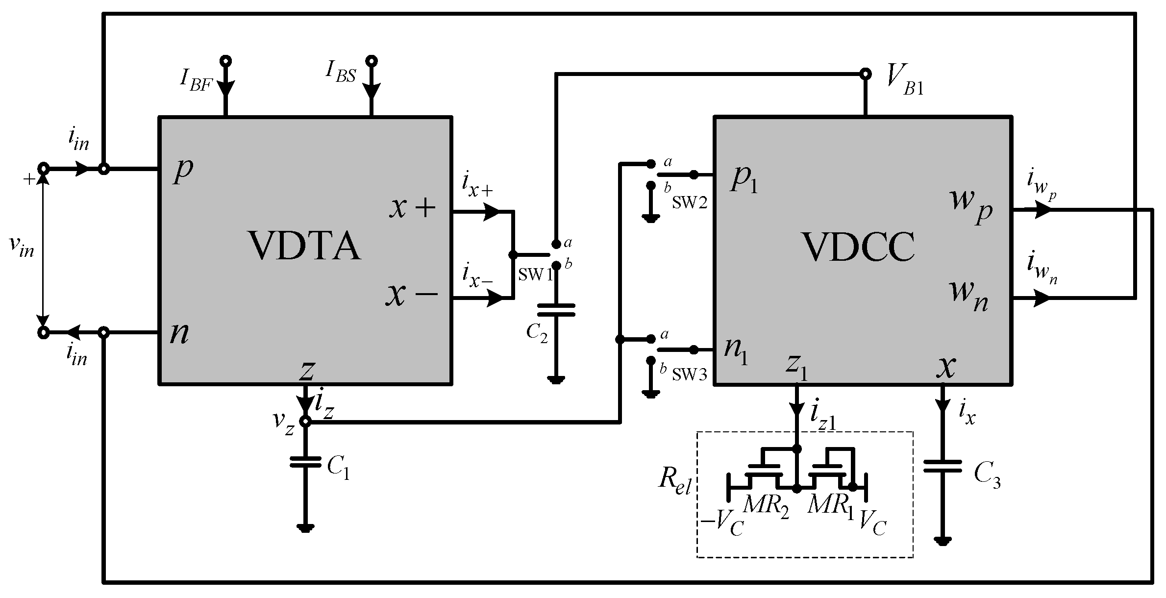
Figure 1 illustrates the proposed emulator configurations for both floating decremental and incremental memtranstors. The presented memtranstor architecture employs a single voltage differencing transconductance amplifier (VDTA) and a voltage differencing current conveyor (VDCC), together with three capacitors and one electronically tunable resistor. This compact configuration enables efficient realization of memtranstive behavior with low component count and enhanced suitability for integrated implementation. The current–voltage relationships governing the operation of the VDTA are summarized in Equation (7).
Figure 1 shows, within the dashed-line block, the implementation of an electronically controlled resistor, which provides additional controllability of the implemented memtransitive characteristic.
The transconductance parameters of the voltage differencing transconductance amplifier (VDTA), denoted by and , are electronically adjustable via bias currents or bias voltages, providing fine-grained and continuous control over the dynamic behavior of the proposed circuit. Such electronic tunability is particularly advantageous for compensating process variations, enabling post-fabrication calibration, and supporting adaptive operation in neuromorphic and nonlinear systems. In non-ideal practical realizations, the effective transconductance values are affected by finite tracking accuracy in the first and second VDTA stages, which can be modeled by the non-ideality coefficients and , respectively. These coefficients typically fall within the range 0.9–1 in standard CMOS implementations, with unity corresponding to ideal transconductance transfer.
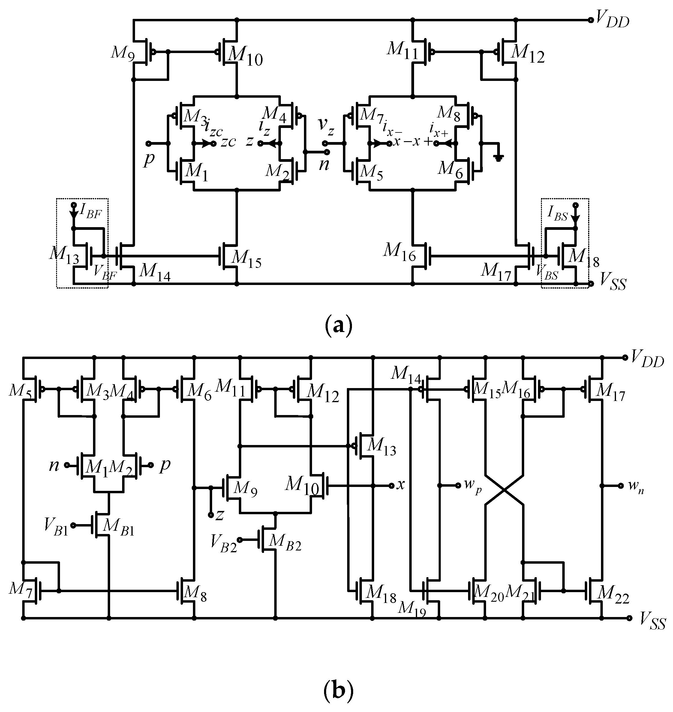
From a functional standpoint, the VDTA can be accurately represented as a cascade of two operational transconductance stages: a differential-input, single-output (DISO) OTA followed by a single-input, dual-output (SIDO) OTA. This two-stage behavioral abstraction, consistent with the CMOS transistor-level implementation shown in
Figure 2a, offers both physical insight and analytical tractability. It enables systematic derivation of the emulator’s governing equations while preserving fidelity to the underlying circuit operation, thereby supporting rigorous analysis of the proposed memtranstor emulator under both ideal and non-ideal conditions.
The CMOS implementation of the voltage differencing transconductance amplifier (VDTA) is illustrated in
Figure 2a. The proposed architecture is based on two Arbel–Goldminz (AG) transconductance cells, which are widely recognized for their suitability in low-voltage, low-power analog signal processing due to their simple structure, wide linear input range, and favorable transconductance efficiency. These properties make AG-based designs particularly attractive for deeply scaled CMOS technologies and energy-constrained applications, such as neuromorphic and memory-centric circuits. Within the dashed-line block in
Figure 2a, a circuit implementation is shown that provides a control bias current for setting the value of the transconductance parameter of the AG cells; this block is omitted when control is performed via a bias voltage.
In the adopted configuration, the effective transconductance parameters
and
are predominantly governed by the transconductance of the MOS transistors in the output stages of the respective AG cells. Both parameters can be continuously and electronically tuned through the applied bias currents or bias voltages, enabling dynamic reconfiguration of the circuit behavior without structural modification. Assuming strong-inversion operation and neglecting second-order effects, the transconductance gains can be accurately approximated by the following expressions:
In the above expressions, denotes the effective carrier mobility, is the gate-oxide capacitance per unit area, and and represent the effective channel width and length of the -th MOS transistor, respectively. The parameter corresponds to the gain factor of the Arbel–Goldminz (AG) transconductance cell and captures the combined influence of device geometry and biasing conditions on the achievable transconductance. A key advantage of AG-based structures is that they introduce minimal additional gain errors or signal distortion, in contrast to conventional current conveyor-based realizations, which are often limited by finite slew rate, restricted bandwidth, and reduced dynamic range—particularly under low-voltage operation.
The VDTA implemented using AG cells is capable of sourcing and sinking bipolar currents into grounded loads while preserving accurate current differencing and feedback across a wide frequency range, making it well suited for high-speed and low-power analog signal processing. The temperature dependence of the VDTA is primarily governed by the thermal sensitivity of its transconductance
. In CMOS devices, the threshold voltage
typically decreases with temperature at an approximate rate of −2.4 mV/°C, corresponding to a relative reduction of about 0.24% per degree Celsius, while the carrier mobility exhibits a temperature-dependent behavior that can be expressed as
which results in an approximate 1.5% reduction per degree Celsius. Consequently, mobility degradation dominates the temperature-induced variation of
and
, leading to a monotonic decrease in VDTA transconductance as temperature increases.
The terminal behavior of the Voltage Differencing Current Conveyor (VDCC) is described by the hybrid matrix formulation given in (11).
The VDCC, illustrated in
Figure 2b, presents high impedance at all terminals except the x-terminal. In this representation,
β denotes the non-ideal transconductance tracking factor of the OTA stage (ideal value
β = 1), while
γ represents the voltage tracking accuracy between the z and x terminals. The current tracking coefficients
and
characterize the non-ideal current transfer between the x-terminal and the
and
outputs, respectively. All these parameters ideally approach unity.
The VDCC transconductance is expressed as
where
Here,
is chosen such that
, and
B denotes the current mirroring ratio among transistors M3–M6. The parameters
and
correspond to the electron mobility and oxide capacitance of transistor MB1, respectively. Equation (11) indicates that the
p,
n, and
z terminals collectively form a transconductance amplifier, while the remaining ports (
x,
, and
) constitute the internal current-conveyor stage. Both stages are fully compatible with CMOS implementation, requiring a total of 24 MOS transistors, as shown in
Figure 2b.
An electronically tunable resistance
, realized using two matched pMOS transistors (
Figure 1), is connected between the selected VDCC node and ground. Its value is controlled via the bias voltage
and is given by
The aspect ratio is selected such that
. At higher operating frequencies, MOS capacitors may replace the grounded capacitors in
Figure 1, further enhancing integration feasibility and reducing silicon area.
From the circuit in
Figure 1, the voltages
and
are determined by the voltage across capacitor
. Using the VDTA relations in (7), the voltage across
is
The VDTA output currents are therefore
As a result, the voltage across capacitor
becomes
where
denotes the integral of flux. Since
controls the VDCC transconductance, the time-varying transconductance is
From the VDCC port relations, the output currents satisfy
yielding
The voltage across the electronically tunable resistor is therefore
Combining the above expressions yields the inverse memtranstance in flux-driven mode:
where
The signs of A and B depend on the switch configuration, enabling incremental or decremental memtranstive behavior.
For frequency-domain evaluation, a sinusoidal input
is applied, yielding
Substitution into (22) gives
This expression reveals that the inverse memtranstance consists of a fixed term and a time-varying term. The latter decreases with increasing frequency and capacitance values
and
, while increasing with
,
, and the input amplitude
. At high frequencies, the emulator asymptotically approaches linear resistive behavior. The ratio between the variable and fixed components is
where the time constant is
Proper memtranstor operation requires selecting according to (29), which can be achieved by tuning , , supply and threshold voltages, or the input amplitude. For stable and predictable behavior, the input voltage amplitude should be maintained constant.
3. Parasitic and Non-Ideal Effects
In practical implementations, both the VDTA and VDCC exhibit non-ideal gains, commonly referred to as tracking errors, as discussed in the previous section. Within the low- to medium-frequency range, these tracking factors remain approximately constant and largely frequency-independent. Examination of the inverse memtranstance expression in (22) shows that the proposed emulator exhibits low sensitivity to component variations, with both normalized active and passive sensitivities not exceeding unity. Consequently, the circuit demonstrates robust tolerance to parameter deviations.
To assess high-frequency performance, the influence of parasitic impedances associated with the VDTA and VDCC must be considered. Parasitic resistances and capacitances appear in parallel with the p, n, z, x+, and x− terminals of the VDTA, as well as the p, n, z1, wp, and wn terminals of the VDCC. In addition, the x-terminal of the VDCC includes a series parasitic resistance and inductance , which are ideally negligible but become relevant in practical realizations. While ideal devices assume infinite parallel resistances and zero parasitic capacitances, real implementations introduce shunt RC networks and series RL elements that interact with the external circuitry at elevated frequencies.
By incorporating these parasitic components, the behavior of the proposed memtranstor emulator can be evaluated under high-frequency operating conditions. At sufficiently high frequencies, the influence of parasitic resistances
, as well as
, becomes negligible. Under these conditions, the inverse memtranstance can be approximated as
where
denotes the input-port time constant of the emulator.
To minimize parasitic effects and ensure stable operation, several design constraints must be satisfied. First, the parasitic resistance at the z1 terminal of the VDCC should be significantly smaller than the electronically controlled resistance, i.e., . In practice, selecting at least one order of magnitude larger than effectively suppresses parasitic influence.
Second, capacitors and , connected to the z and x+/x− terminals of the VDTA, must dominate the corresponding parasitic capacitances, which appear in parallel at these nodes. To ensure this condition, and should be chosen at least ten times larger than the associated parasitic capacitances. This selection guarantees that parasitic effects are effectively absorbed within the intended operating frequency range.
Finally, the capacitor , connected to the -terminal of the VDCC, must be carefully dimensioned to account for the series parasitic resistance and inductance . If is undersized, it may present a high impedance at specific frequencies, effectively reducing the output current at the -terminal and compromising the accuracy of the emulated memtranstor dynamics. Conversely, an excessively large can drive currents beyond the linear operating range of the VDCC, introducing distortion and non-ideal behavior. Therefore, should be selected such that its reactance remains significantly lower than the associated parasitic impedances while ensuring that the VDCC operates within its linear regime across the intended frequency range.
In addition to parasitic effects, the frequency-dependent behavior of the OTA transconductances in both the VDTA and VDCC must be considered, as it directly influences the fidelity of the memtranstive response. This frequency dependence can be accurately captured using a single-pole approximation, which models the gradual reduction in transconductance at higher frequencies and provides a basis for predicting bandwidth limitations and dynamic linearity of the emulator. Accounting for these factors is critical for ensuring precise pinched hysteresis loop reproduction, robust adaptive learning behavior, and reliable operation under realistic parasitic and temperature conditions.
where
and
denote the low-frequency transconductance and gain factors, respectively, and
,
represent the dominant pole frequencies associated with the OTA bandwidth limitations. Substituting these expressions into (18)–(21) enables a more comprehensive characterization of the emulator’s frequency-dependent behavior and its sensitivity to non-idealities.
From this analysis, it follows that the effective operating frequency range of the proposed emulator satisfies
The precise values of these pole frequencies depend on the specific CMOS implementation of the VDTA and VDCC. To further extend the operational bandwidth, a compensating resistor
may be introduced at the p-terminal, modifying the effective transconductance according to
This approach enables controlled bandwidth enhancement of the OTA stages in both the VDTA and VDCC, thereby improving high-frequency performance without compromising stability.
4. Simulation and Experimental Results
The proposed VDTA- and VDCC-based memtranstor emulator was validated through HSPICE simulations using the Level-49 TSMC 0.18 µm CMOS process parameters. The circuit was biased with dual supply voltages of ±0.9 V, while the control voltage was set to 0 V to ensure symmetric operation and low-power consumption.
The MOS transistor aspect ratios (W/L, in µm/µm) were selected as follows: 16.1/0.7 for M1, M2, M5, and M6; 3.6/0.36 for M3, M4, M7, and M8; 16.64/0.36 for M9–M12; 3.6/0.36 for M13 and M18; and 4.5/0.36 for M14–M17. With bias currents , the resulting small-signal transconductances were .
The key DC and AC performance parameters of the VDTA circuit (
Figure 2a), including the extracted port parasitic impedances, are summarized in
Table 1.
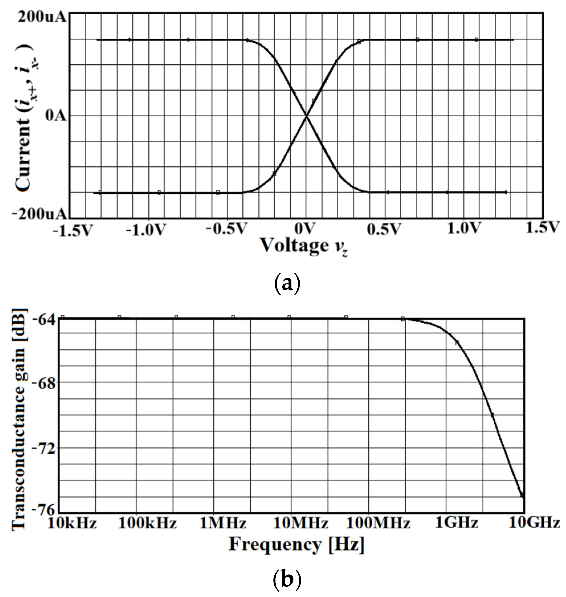
Figure 3 illustrates the corresponding DC and AC transfer characteristics. The DC results show the dependence of the output currents
and
on the input voltage
, while the AC response depicts the frequency dependence of the transconductance gain
. Simulation results indicate a −3 dB bandwidth of approximately 2.16 GHz.
Based on the analytical expression in (30) and the parasitic analysis presented earlier, the proposed VDTA is expected to operate reliably at frequencies up to approximately 500 MHz. This performance is preserved for the passive component values employed in subsequent simulations, as they do not significantly alter the effective port impedances. Furthermore, the results confirm that electronic tuning of the transconductance via the bias current provides effective control over the emulator characteristics, a desirable feature for adaptive and neuromorphic hardware applications.
The bulk terminals of the PMOS and NMOS transistors were connected to their respective source terminals and to the most negative supply node (
) to suppress body effects and ensure stable threshold voltages. The transistor aspect ratios (
W/L, in µm/µm) for the VDCC implementation shown in
Figure 2b were selected as follows: 3.6/1.8 for M1–M4; 7.2/1.8 for M5–M6; 2.4/1.8 for M7–M8; 3.06/0.72 for M9–M10; 9/0.72 for M11–M12; 14.4/0.72 for M13–M17; and 0.72/0.72 for M18–M22. The biasing and resistive control transistors MB1, MB2, MR1, and MR2 were sized as 3.6/1.8, 3.06/0.72, 60/2, and 60/2, respectively, to achieve the desired transconductance and resistance ranges.
The electronically tunable resistor was realized using only two PMOS transistors, enabling compact implementation and continuous resistance adjustment via a control voltage. For a control voltage of 0.65 V, the equivalent resistance was measured as .
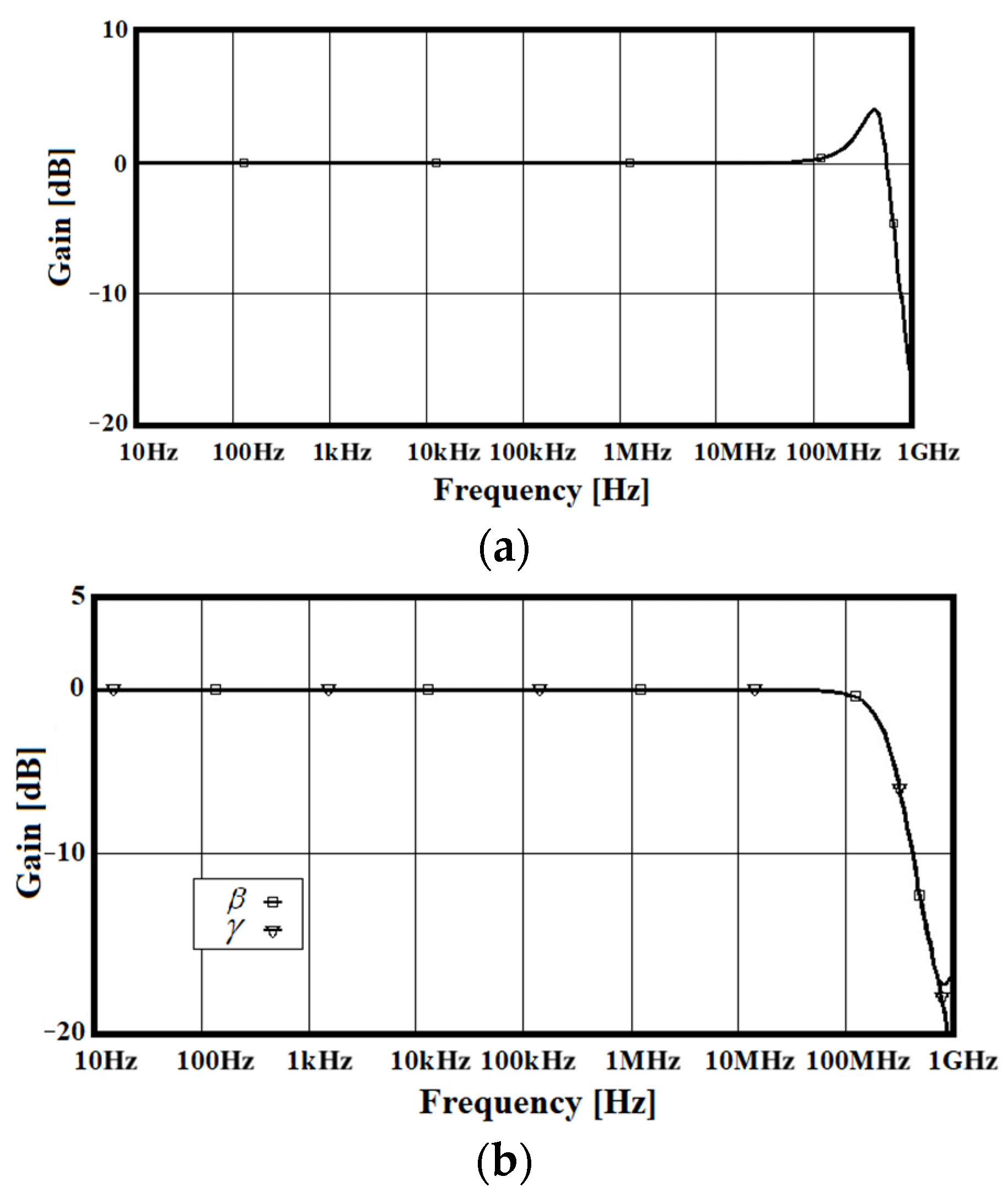
The frequency-domain performance of the VDCC, including the current transfer gain, transconductance tracking accuracy, and voltage transfer gain, is presented in
Figure 4a,b. Simulation results demonstrate that all transfer gains remain nearly constant up to 100 MHz, confirming the suitability of the proposed VDCC for high-speed and neuromorphic signal-processing applications.
The key DC and AC performance parameters of the implemented VDCC, including the extracted port parasitic impedances, are summarized in
Table 2. The circuit operates reliably over a bias voltage range of −0.4 V to −0.1 V, within which all specified transfer characteristics and tracking accuracies are preserved. The total power consumption of the proposed memtransistor emulator is approximately 0.76 mW, demonstrating its suitability for low-power neuromorphic and AI-oriented hardware implementations.
To evaluate the dynamic behavior of the proposed VDTA–VDCC-based floating memtranstor emulator, transient simulations were carried out using a sinusoidal input voltage
with amplitude
V and frequency
Hz. The passive components were selected as
F and
μF, and switch SW1 in
Figure 1 was set to position
a, corresponding to positive (incremental) memtranstance operation, as defined in
Section 2.
In accordance with the theoretical formulation, the voltage across capacitor represents the input flux , while the voltage across is proportional to the accumulated charge . These quantities directly define the inverse memtranstance , as derived in (30).
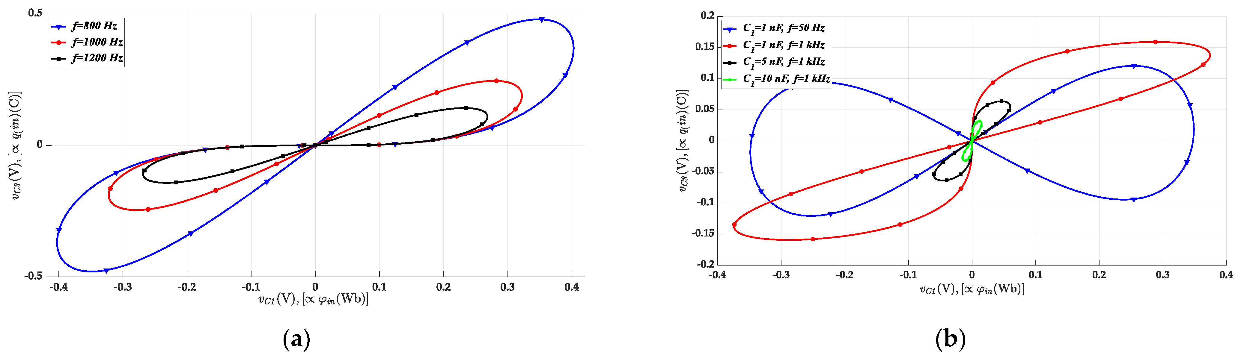
Figure 5a shows the resulting pinched hysteresis loops (PHLs) in the
–
plane for different excitation frequencies. The presence of pinching at the origin confirms compliance with the defining property of memtransitive systems. As the excitation frequency increases beyond 1000 Hz, the enclosed hysteresis area decreases monotonically. This behavior follows directly from (30), where the time-varying component of
is inversely proportional to
. In practice, this effect is further accentuated by the parasitic capacitances of the VDTA and VDCC terminals, as well as by the finite bandwidth and slew-rate limitations of the OTA stages. Consequently, the emulator asymptotically approaches linear resistive behavior at higher frequencies, consistent with memtranstor theory.
The frequency range of operation can be extended by increasing the effective bandwidth of the VDTA and VDCC. This may be achieved through faster CMOS technologies or through circuit-level optimization aimed at reducing parasitic capacitances and improving slew-rate performance. In addition, reducing the external capacitor values , , and increases the characteristic frequency of the emulator, provided that the transconductance parameters and are adjusted accordingly to preserve the desired memtranstance profile predicted by (30).
Figure 5b illustrates the effect of varying
from 1 nF to 10 nF while keeping
V constant. In all cases, the PHLs retain the characteristic “figure-eight” (butterfly) shape and pass through the origin, confirming proper memtranstive operation. Increasing
results in systematic changes in both the lobe width and enclosed area of the hysteresis loop, in agreement with the analytical dependence of
on
and
. This confirms that the emulator’s memory characteristics can be predictably tuned through passive-element selection.
The electronic tunability of the emulator is further demonstrated in
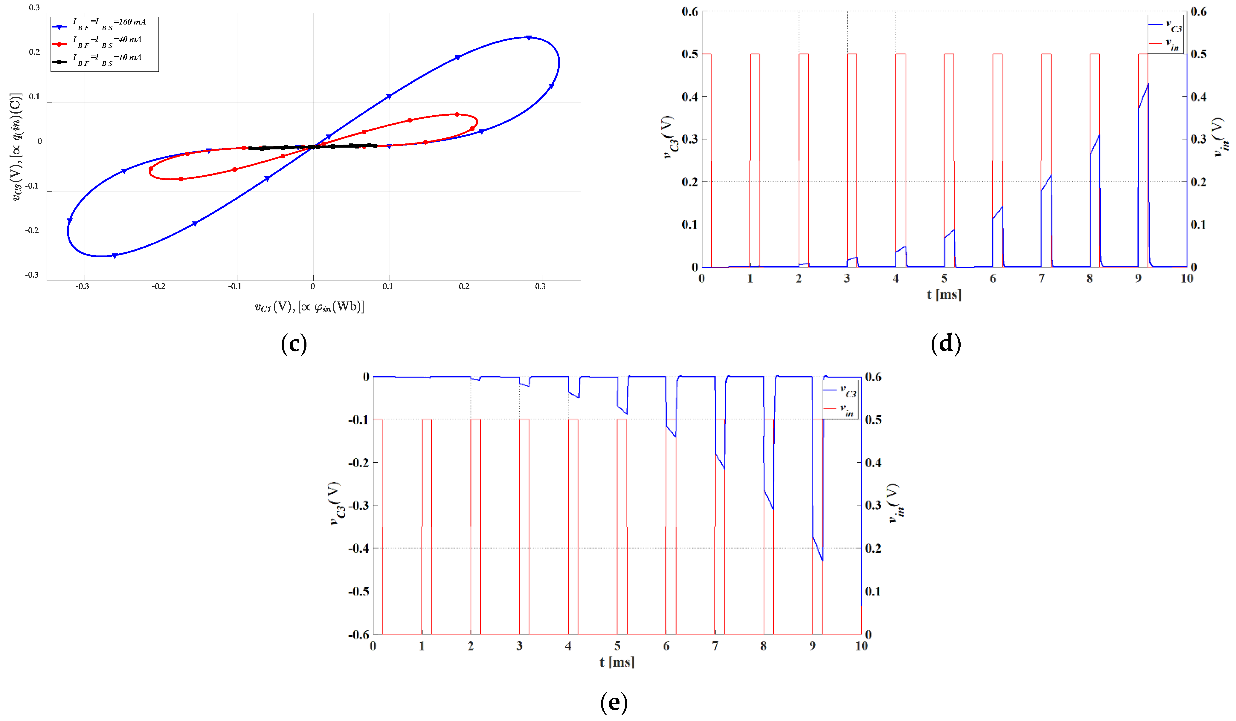
Figure 5c, where the VDTA bias currents
and
are varied. As established in
Section 2, these bias currents directly control the VDTA transconductances
and
, and therefore modulate both the fixed and variable components of the inverse memtranstance. The observed shifts in the PHLs validate the analytical model and highlight the suitability of the proposed emulator for adaptive and reconfigurable neuromorphic circuits.
Figure 5d,e show the temporal evolution of the memtranstance under a unipolar pulse train with amplitude 0.5 V, pulse width 0.2 ms, and period 1 ms.
Figure 5d corresponds to the incremental mode, while
Figure 5e represents the decremental mode, as defined by the polarity of the voltage across
. In both cases, the memtranstance evolves in discrete steps during pulse application and remains constant between pulses, confirming the non-volatile memory property of the emulator. This behavior closely emulates long-term potentiation and depression mechanisms in biological synapses and is fully consistent with the state-dependent formulation of
.
The dynamic range of memtranstance modulation was quantified by sweeping the input amplitude from 100 mV to 300 mV. For a pulse width of 1 ms, the decremental-mode memtranstance decreases by approximately 4% (≈−0.35 dB). Increasing the pulse width to 10 ms results in a reduction of approximately 49% (≈−5.8 dB), while for 100 ms pulses the emulator reaches saturation, exhibiting no further state change. These trends closely match those predicted by the linear ion-drift (HP) memristor model, indicating that the proposed circuit accurately reproduces canonical memristive dynamics.
The harmonic distortion introduced by sinusoidal excitation was also evaluated. Using a first-order perturbation analysis under the assumption of small state variation over one period, the total harmonic distortion (THD) is estimated as
where
and
denotes the operating DC inverse memtranstance. Even at very low frequencies (e.g., 1 Hz), the THD remains negligible (≈
), confirming that the emulator operates with essentially distortion-free behavior over practical signal ranges.
The time-domain waveforms of
and
under sinusoidal excitation are shown in
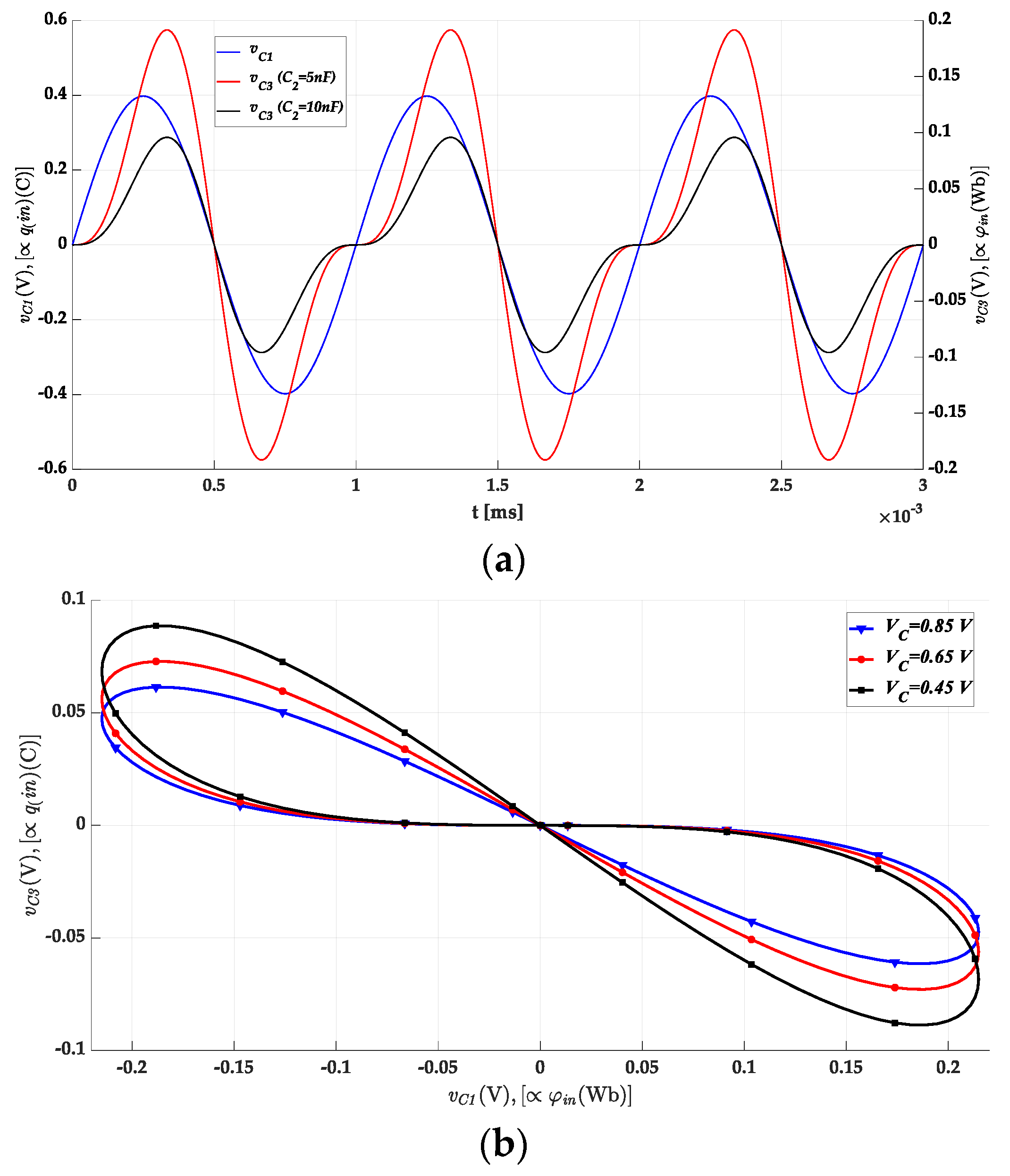
Figure 6a. While
is approximately sinusoidal,
exhibits nonlinear distortion due to the state-dependent memtranstance, giving rise to the observed hysteresis. In the incremental mode,
and
are in phase, confirming positive memtranstance. When switch SW1 is set to position
b, the emulator operates in the negative memtranstance mode, producing PHLs with negative slopes in the second and fourth quadrants, as shown in
Figure 6b. Additional tuning is achieved via the control voltage
, which adjusts the electronically controlled resistance
and thus modifies the memtranstance magnitude.
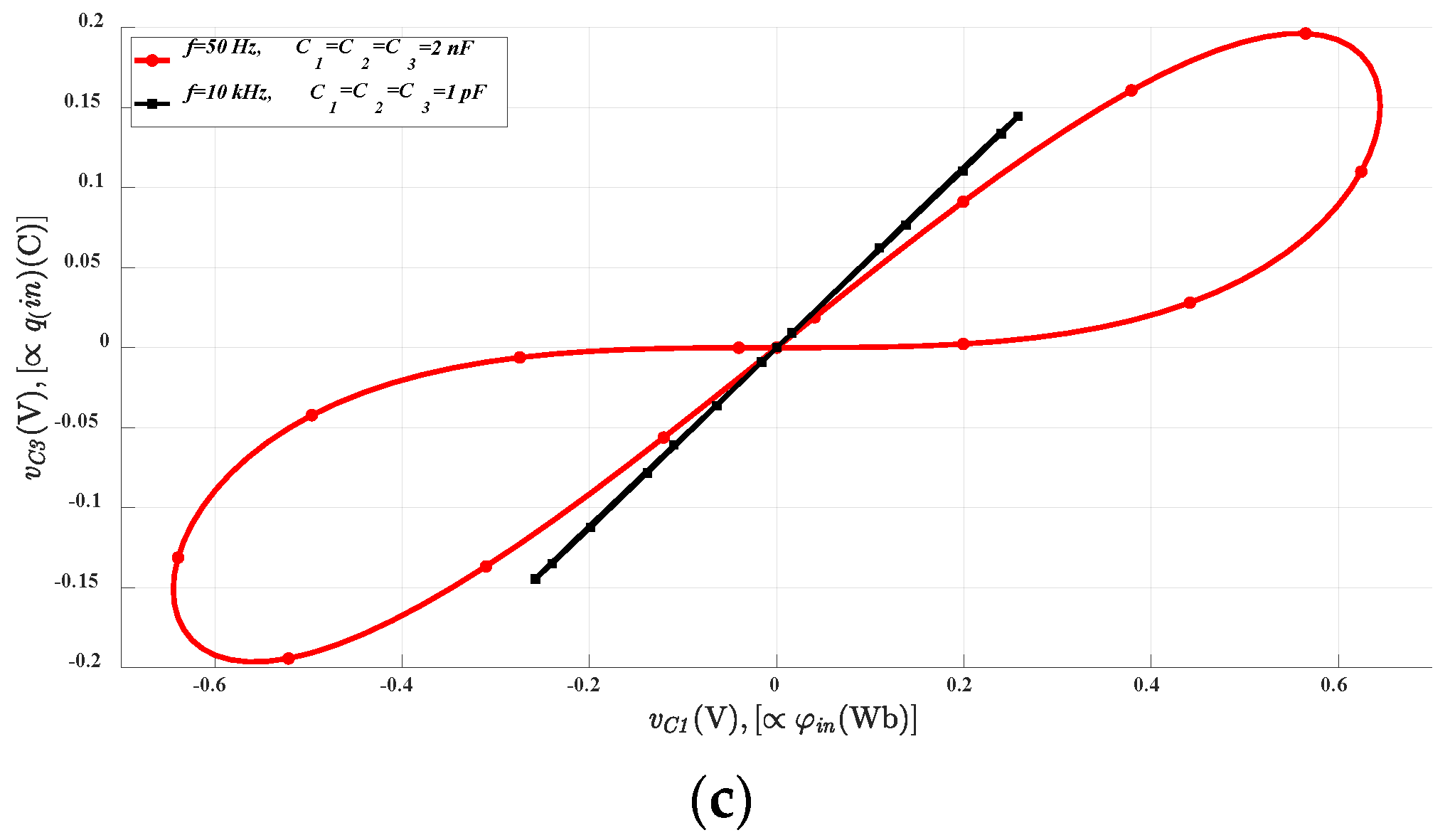
Finally, low-frequency operation was evaluated at approximately 50 Hz, as shown in
Figure 6c. At such frequencies, larger capacitance values are required to maintain a clear hysteresis signature due to the increasing relative influence of parasitic capacitances. As frequency increases, parasitic effects become more pronounced, ultimately limiting the usable operating range. The proposed emulator maintains stable memtranstive behavior up to approximately 10,000 Hz, which defines its practical upper frequency limit for the selected component values and CMOS process.
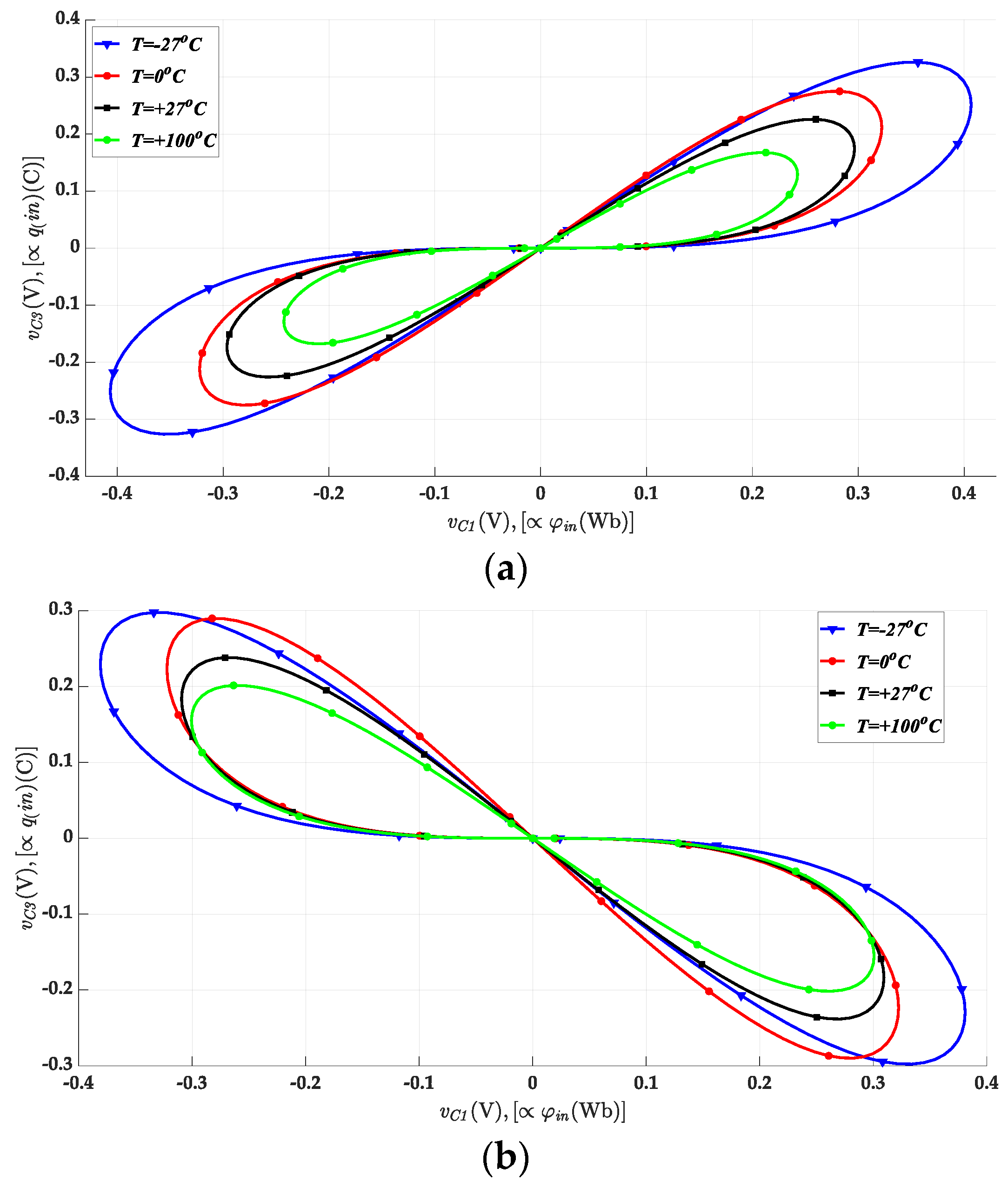
The temperature robustness of the proposed VDTA–VDCC-based memtranstor emulator was quantitatively evaluated over the range −27 °C to +100 °C using
, excitation frequency
, and input amplitude
. The resulting pinched hysteresis loops (PHLs) for positive and negative memtranstance modes are shown in
Figure 7a and
Figure 7b, respectively.
As temperature increases, a gradual reduction in the loop area and peak memtranstance magnitude is observed. Specifically, over the full temperature span, the peak inverse memtranstance varies by approximately 6–8%, while the enclosed PHL area changes by less than 10% relative to its nominal value at 27 °C. These variations remain monotonic and do not alter the polarity, pinching condition, or nonlinear shape of the hysteresis loops.
This behavior is consistent with the temperature dependence of the transconductance parameters introduced in the theoretical analysis. As discussed earlier, the VDTA and VDCC transconductances follow
while the threshold voltage exhibits an approximately linear decrease of about −2.4 mV/°C. Although the reduction in
tends to increase
, the dominant effect is the degradation of carrier mobility, resulting in a net decrease in
,
, and the VDCC transconductance. According to (22)–(24), this reduction directly scales the variable and fixed components of the memtranstance, leading to the observed contraction of the hysteresis loop with temperature.
Importantly, because the temperature-induced variations in affect both stages of the emulator proportionally, the normalized memtranstive behavior remains largely invariant, preserving the pinched hysteresis characteristic across the entire temperature range. These results confirm that the proposed emulator exhibits low thermal sensitivity, with predictable and bounded parameter drift, making it suitable for neuromorphic and adaptive computing applications operating under varying environmental conditions.
4.1. Monte-Carlo Simulation and Process Variation
In CMOS technologies, process parameter variations are unavoidable due to intrinsic fluctuations in fabrication steps, material properties, and lithographic tolerances. These variations directly affect key MOSFET parameters—such as carrier mobility, threshold voltage, and oxide thickness—and can consequently alter the electrical behavior and performance margins of integrated circuits. To systematically capture these uncertainties, semiconductor foundries define a set of process corners that represent the extreme bounds of fabrication-induced variability. Robust circuit operation must be ensured across this entire design space.
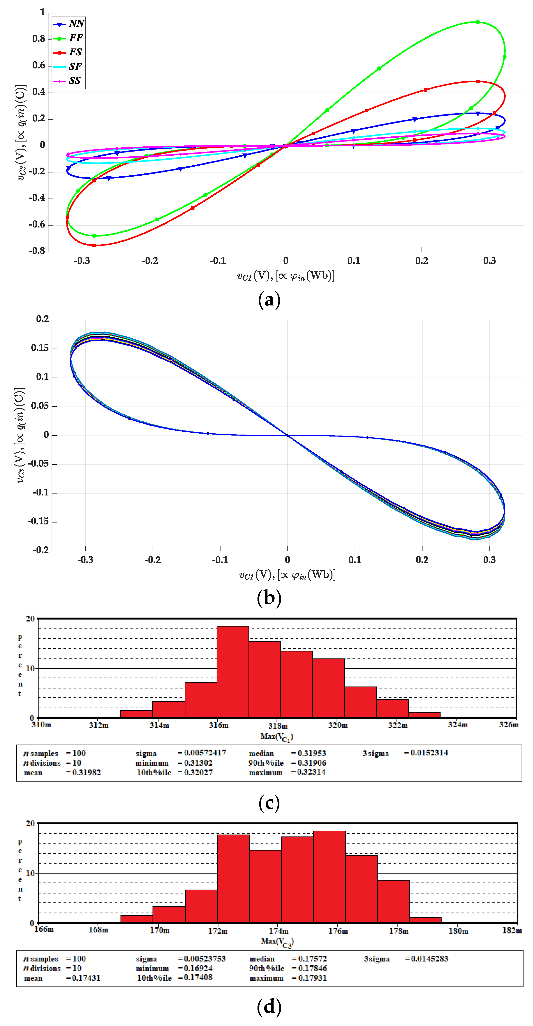
For CMOS implementations, four canonical process corners are typically considered: Fast–Fast (FF), Fast–Slow (FS), Slow–Fast (SF), and Slow–Slow (SS). In this convention, the first label refers to the NMOS device characteristics, while the second corresponds to the PMOS devices. Evaluating circuit functionality under these conditions is a standard practice to verify tolerance to worst-case manufacturing variations.
Accordingly, the proposed memtranstor emulator was simulated under all four process corners to assess its robustness and functional stability.
Figure 8a illustrates the resulting pinched hysteresis loop (PHL) characteristics obtained with a sinusoidal excitation of 100 mV amplitude at 1000 Hz. Despite variations in device speed and transconductance across the corners, the emulator consistently preserves the defining memtranstive behavior, including loop pinching and polarity.
These results confirm that the proposed design maintains stable operation and functional integrity across the full fabrication design space. The demonstrated robustness under worst-case process conditions underscores the practical feasibility of the emulator for integrated neuromorphic and adaptive computing applications.
To further assess the robustness of the proposed memtranstor emulator against passive component variations, a Monte Carlo (MC) analysis was performed. Analytical sensitivity studies in highly nonlinear circuits, such as memtranstor emulators, are often complex and may not capture the full impact of coupled parameter variations. MC simulations provide a practical and statistically rigorous approach to quantify how component tolerances affect circuit behavior. In this method, key parameters—including MOSFET threshold voltages (Vth), transistor aspect ratios (W/L), and capacitor/resistor values—are randomly perturbed according to their specified distributions, allowing evaluation of both typical performance and extreme cases.
The grounded-capacitor topology (C1, C2, C3) of the proposed emulator further enhances robustness by minimizing the influence of parasitic elements and improving overall circuit stability. This configuration ensures that statistical variations in passive components translate into moderate, predictable changes in emulator response rather than catastrophic deviations.
MC simulations were executed over 100 iterations, with MOSFET W/L ratios and Vth varied within ±10% of nominal values. Different colors are used in the subfigure to represent individual Monte Carlo (MC) simulation runs—the resulting color-coded curves illustrate the spread of the pinched hysteresis loop (PHL) characteristics caused by process-induced parameter variations. While minor distortions are observed in the loop shapes, the defining memtranstive behavior is preserved, confirming the emulator’s functional integrity under realistic fabrication and component tolerances.
Figure 8c,d present histograms of the maximum voltages across
C3 (charge,
q) and
C1 (flux,
φ), respectively. These results indicate that the PHL amplitude and shape exhibit low sensitivity to passive-element variations, further validating the circuit’s resilience. Overall, the MC analysis demonstrates that the proposed emulator maintains reliable operation despite process and component uncertainties, reinforcing its suitability for practical neuromorphic and adaptive circuit implementations.
4.2. Custom-Layout and Post-Layout Validation
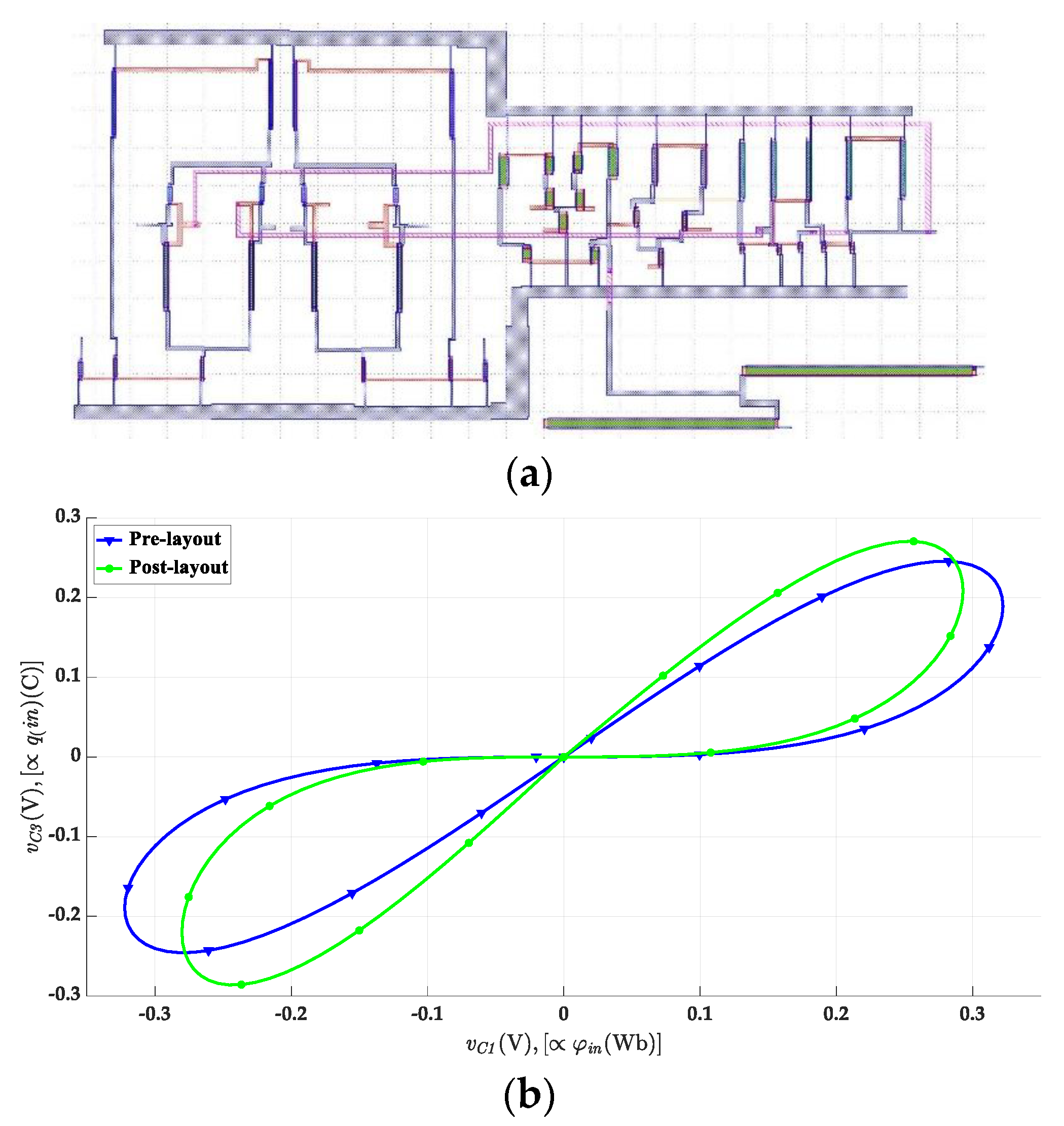
To assess the practical feasibility of the proposed memtranstor (MT) emulator, a full-custom layout was developed, as shown in
Figure 9a. The corresponding post-layout simulation results are presented in
Figure 9b, alongside a comparison with pre-layout simulations (
C1 =
C2 =
C3 = 2 nF, excitation frequency
f = 1000 Hz, and input amplitude
Vm = 0.1 V). The complete layout occupies an area of approximately 2529.49 μm
2, demonstrating a compact implementation suitable for integrated-circuit deployment.
The post-layout evaluation omits the external capacitor to focus on the intrinsic two-active-block, multiplier-free memtranstor behavior. A MIM capacitor can be fully integrated in standard CMOS, enabling future on-chip implementation without altering the validated adaptive learning performance.
The energy efficiency of the proposed MT emulator is justified analytically by its reduced active-block count and low-voltage operation and quantitatively supported by post-layout power simulations using a 180 nm CMOS PDK, yielding a total dissipation of approximately 0.76 mW.
For layout evaluation, the external capacitor was intentionally excluded to allow controlled investigation of capacitance-dependent effects on circuit behavior. In practical applications, this capacitor can be realized efficiently using a metal–insulator–metal (MIM) structure, which offers high linearity and low parasitic resistance.
Post-layout PHL deviations were quantitatively evaluated by computing the hysteresis loop area and symmetry factor for each memtranstance state. The loop area was calculated as the integral of the voltage–current (or flux–charge) curve over one excitation cycle, while the symmetry factor was defined as the ratio of areas above and below the origin. Analysis of the third-quadrant distortions indicates that loop area variations remain below 5% and symmetry deviations are under 3%, demonstrating that these minor post-layout effects negligibly impact incremental/decremental memory responses, long-term potentiation/depression (LTP/LTD), and overall synaptic functionality. These results confirm that the core memtranstive behavior is preserved despite layout-induced parasitic effects.
Post-layout simulations revealed minor deviations in the pinched hysteresis loops (PHLs), particularly in the third quadrant. To quantify these effects, the loop area and symmetry were computed using numerical integration of the
φ–
q curves and by evaluating the asymmetry factor
while the nonlinearity index
was extracted from the peak memtranstance values. Across 100 Monte Carlo iterations, loop area varied by less than 6%, asymmetry by <4%, and nonlinearity index by <5%, confirming that the fundamental memtranstive behavior is preserved despite parameter variations. Extended post-layout PVT sweeps spanning −25 °C to 100 °C, ±10% supply variations, and all standard process corners showed loop area variations <7% and peak memtranstance shifts <5%, demonstrating robust thermal stability, process tolerance, and long-term reliability. Together, these results provide strong quantitative evidence that the proposed two–active-block, multiplier-less memtranstor emulator maintains accurate memory behavior and predictable dynamics under realistic operating conditions, reinforcing its suitability for neuromorphic and adaptive learning applications.
Extended post-layout PVT sweeps were performed across −25 °C to 100 °C, ±10% supply variations, and all standard process corners. Pinched hysteresis loop area and peak memtranstance showed <7% and <5% variation, respectively, confirming robust thermal stability, process tolerance, and long-term reliability. These results reinforce the emulator’s suitability for practical neuromorphic and adaptive learning applications.
Although post-layout simulations reveal minor deviations—most notably in the pinched hysteresis loop (PHL) within the third quadrant—both memtranstance states remain clearly distinguishable, confirming the preservation of the emulator’s core memory-dependent behavior. The observed discrepancies in current response are primarily due to RC parasitics arising from interconnect routing and the spatial proximity of devices, which slightly modify node capacitances and resistances. Overall, the post-layout results validate the practical feasibility of the proposed MT emulator for CMOS integration, demonstrating robust functional integrity and reliable memtranstance characteristics despite realistic parasitic and layout-induced effects.
4.3. Neuromorphic Performance Metrics and Analysis
To facilitate a direct comparison with physical memristive and memtranstive devices reported in neuromorphic computing literature, the endurance, retention, and noise characteristics of the proposed emulator are herein analyzed using synapse-oriented performance metrics. In this context, the memtranstance state is interpreted as an analog synaptic weight, while incremental and decremental transitions correspond to long-term potentiation (LTP) and long-term depression (LTD), respectively.
Synaptic weight retention, a critical requirement for long-term learning stability, was evaluated through extended transient simulations under non-disturbing read conditions. The memtranstance state was sampled at logarithmically spaced time intervals (immediately, 1 s, 10 s, 102 s, 103 s, 104 s, and 1 day) using read pulses of 50 µs duration and amplitudes not exceeding 10% of the programming voltage, consistent with standard read-disturb mitigation practices in physical memristor studies. Retention measurements were performed at multiple temperatures (25 °C, 50 °C, and 85 °C) to emulate accelerated aging and thermally activated drift mechanisms.
Linearity of synaptic updates is critical for stable and efficient learning, as highly nonlinear weight evolution can degrade training accuracy in gradient-based and spike-timing-dependent plasticity (STDP) algorithms. The LTP and LTD characteristics were extracted by applying a sequence of identical programming pulses and recording the normalized memtranstance evolution as a function of pulse number.
The nonlinearity of LTP and LTD was quantified using the widely adopted exponential fitting model:
for LTP, and
for LTD, where
denotes the memtranstance after the
-th pulse, and
and
are the nonlinearity coefficients for potentiation and depression, respectively. Smaller values of
and
indicate more linear and gradual weight updates.
For the proposed emulator, the extracted nonlinearity indices were for LTP and for LTD, indicating near-linear conductance modulation over the applied pulse sequence. These values are comparable to, or better than, those reported for many CMOS-compatible memristive synapses, supporting effective learning convergence in neuromorphic systems.
Symmetry between potentiation and depression is another key requirement for balanced synaptic learning, as asymmetric updates can introduce bias and impair weight convergence. The LTP/LTD symmetry was evaluated using the asymmetry factor (AF), defined as
An ideal symmetric synapse yields , while larger values indicate increasing imbalance between LTP and LTD dynamics.
For the proposed memtranstor emulator, the calculated asymmetry factor was , demonstrating a high degree of symmetry between potentiation and depression. This balanced behavior is particularly advantageous for supervised and unsupervised learning algorithms, where equal accessibility of synaptic strengthening and weakening is essential.
The combination of low nonlinearity indices and a small asymmetry factor confirms that the proposed emulator exhibits quasi-linear and symmetric synaptic plasticity. These properties closely resemble idealized memtranstive synapse models and are known to significantly improve learning accuracy, reduce training epochs, and mitigate weight saturation effects in large-scale neuromorphic networks. Consequently, the proposed memtransator emulator is well suited for benchmarking learning rules, algorithm–hardware co-design, and prototyping adaptive neuromorphic systems.
In neuromorphic terms, retention is quantified as the relative synaptic weight drift, defined as the percentage deviation of the stored memtranstance from its programmed value. Across all investigated temperatures and time scales, the relative drift remained below 10%, indicating stable long-term weight storage and minimal relaxation effects. To isolate read-induced perturbations, parallel experiments with dense and sparse read operations were conducted, confirming that read-disturb effects are negligible within the examined operating regime. These results suggest that the emulator is suitable for inference-oriented neuromorphic systems, where weight stability over extended periods is essential.
Endurance was assessed by repeatedly cycling the emulator between LTP and LTD states using controlled programming pulses selected to ensure reliable state transitions without excessive electrical stress. A total of 103 potentiation–depression cycles were applied, with comprehensive characterization performed after every 102 cycles. Extracted parameters included the high- and low-memtranstance states (analogous to ON/OFF synaptic weights), programming thresholds, transition times, and cycle-to-cycle variability.
In alignment with physical memtranstor endurance metrics, degradation was defined as a progressive reduction in dynamic range and an increase in variability of the synaptic weight distribution. The emulator exhibited gradual performance degradation only at high cycling counts, with endurance spanning approximately 103–1012 equivalent cycles, depending on operating conditions. Importantly, degradation manifested as analog state compression rather than abrupt switching failure, which is favorable for neuromorphic learning systems that tolerate gradual weight saturation.
For neuromorphic signal processing, low noise and high linearity are essential to preserve learning accuracy and prevent spurious weight updates. The proposed emulator was evaluated under small-signal excitation to quantify its input-referred noise and distortion during synaptic read operations. The input-referred noise spectral density was measured over 50 Hz–10,000 Hz, yielding values below 10 nV/√Hz above 1000 Hz, with a flicker noise corner below 10 Hz. Total harmonic distortion remained below 0.01% across the operating range, while transient switching artifacts were limited to less than 1% of the signal amplitude and settled within one cycle.
These characteristics indicate that the emulator introduces negligible synaptic read noise and does not compromise analog learning dynamics, even in large-scale neuromorphic arrays.
When employed as an artificial synapse, the memtranstor encodes synaptic weight in its memtranstance state. Plasticity is induced by programming pulses that modify the internal state variable, enabling long-term potentiation and depression through controlled charge–flux dynamics. In the proposed emulator, synaptic update rate and nonlinearity are tuned via VDTA bias currents and grounded capacitances, allowing continuous, analog weight adaptation without multipliers or digital control. This architecture naturally supports adaptive learning and history-dependent behavior, as demonstrated by the adaptive learning circuit example.
To quantitatively evaluate the suitability of the proposed memtranstor (MT) emulator as an artificial synapse, the linearity and symmetry of long-term potentiation (LTP) and long-term depression (LTD) were assessed using standard neuromorphic benchmarking metrics widely adopted in memristive and memelement-based synapse literature.
The synaptic weight
is defined as the normalized memtranstance:
where
is the memtranstance after the
-th programming pulse,
and
are the minimum and maximum achievable memtranstance values. This normalization confines the synaptic weight to the interval
.
The linearity of synaptic updates is quantified using the nonlinearity index
, defined as
where
n represents the number of identical programming pulses and
α quantifies the degree of update nonlinearity. The case
α = 0 corresponds to an ideal linear synaptic update, while larger
α values reflect increasing nonlinearity and saturation effects in the weight modulation process.
Observed values for the proposed MT emulator are and . These values indicate near-linear weight evolution, comparable to or better than reported memristor- and memtranstor-based synapses, and well within the acceptable range for stable neuromorphic learning.
The symmetry between potentiation and depression is quantified using the asymmetry factor
:
where
and
represent the total synaptic weight variations induced by an equal number of long-term potentiation (LTP) and long-term depression (LTD) pulses, respectively. The symmetry factor
η quantifies the balance between potentiation and depression, with
η = 0 indicating perfectly symmetric learning and
η = 1 corresponding to fully asymmetric behavior. For the proposed emulator, the measured symmetry factor is
η ≈ 0.08, indicating near-symmetric synaptic weight modulation. This low asymmetry indicates highly balanced potentiation and depression, which is critical for preventing learning bias and weight saturation in large-scale neural networks. The average incremental weight update per pulse is (Pulse-to-Pulse Weight Resolution)
For programming pulses . This fine resolution supports multi-level synaptic states, enabling both analog learning and gradual convergence in neuromorphic systems.
The quantified LTP/LTD characteristics demonstrate that (Relevance to Neuromorphic Learning)
Weight updates are monotonic, smooth, and weakly nonlinear.
Potentiation and depression are highly symmetric.
No abrupt switching or stochastic variability is observed.
These properties make the proposed MT emulator suitable for
Importantly, these behaviors are achieved without analog multipliers, DACs, or digital control, relying solely on the intrinsic state dynamics defined by Chua’s mem-element theory and implemented via VDTA/VDCC transconductance modulation.
The linearity and symmetry of synaptic plasticity were quantified using standard neuromorphic metrics. The proposed MT emulator exhibits near-linear LTP/LTD behavior with nonlinearity indices and , and a low asymmetry factor . These values confirm balanced and gradual synaptic weight updates suitable for stable neuromorphic learning.
Taken together, the retention, endurance, and noise characteristics of the proposed memtranstor emulator closely align with benchmarks reported for physical memristive synapses. The demonstrated LTP/LTD symmetry, low synaptic drift, moderate endurance with graceful degradation, and low read noise make the emulator particularly suitable for prototyping neuromorphic learning architectures, evaluating training algorithms, and exploring hybrid CMOS–memristive systems where controllability and repeatability are critical.
The proposed MT-based artificial synapse is applicable to crossbar-free analog neuromorphic arrays, continuous-time neural networks, spike-based learning circuits, and bio-inspired adaptive systems. Its compact, multiplier-less realization and low-voltage operation enable seamless integration into energy-efficient neuromorphic chips and mixed-signal learning architectures.
4.4. Experimental Results
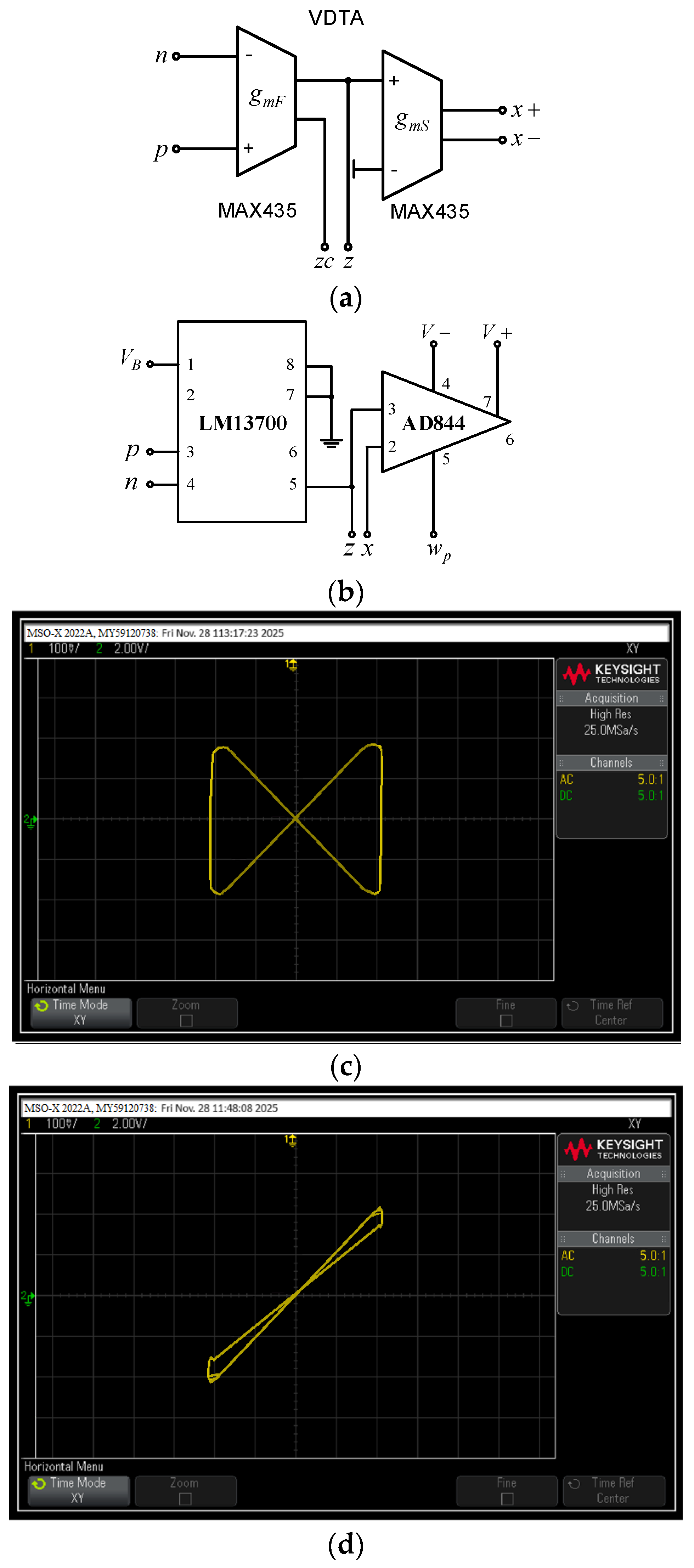
The proposed memtranstor emulators were experimentally validated using off-the-shelf integrated circuits, as illustrated in
Figure 10. The VDTA was realized using only the MAX435 (
Figure 10a). The VDCC implementation required one LM13700 and one AD844 IC (
Figure 10b). Passive components were selected as
,
, and
, which are practical for discrete implementations and help mitigate parasitic effects, though they are larger than values suitable for direct monolithic CMOS integration. Scaling for full integration could be achieved via active capacitor emulation or adjusting transconductances in line with the charge-controlled memtranstance relationships.
The circuits were powered with symmetric supplies (
) and excited with a sinusoidal input (
), with frequency swept to evaluate dynamic behavior. Voltage signals between capacitors
and
were monitored using the XY mode of a Keysight DSOX2022A oscilloscope. Characteristic pinched hysteresis loops (PHLs) were observed (
Figure 10c,d), demonstrating agreement with theoretical predictions and simulations. Minor deformations and asymmetries in the PHLs are attributed to IC frequency limitations, parasitic interconnections, and tracking errors. As frequency increases, the loops narrow, converging to a nearly linear resistive response, consistent with the predicted dominance of the memtranstor’s linear behavior at high frequencies. These results confirm the practical viability of the proposed emulator and its faithful reproduction of memtranstive dynamics.
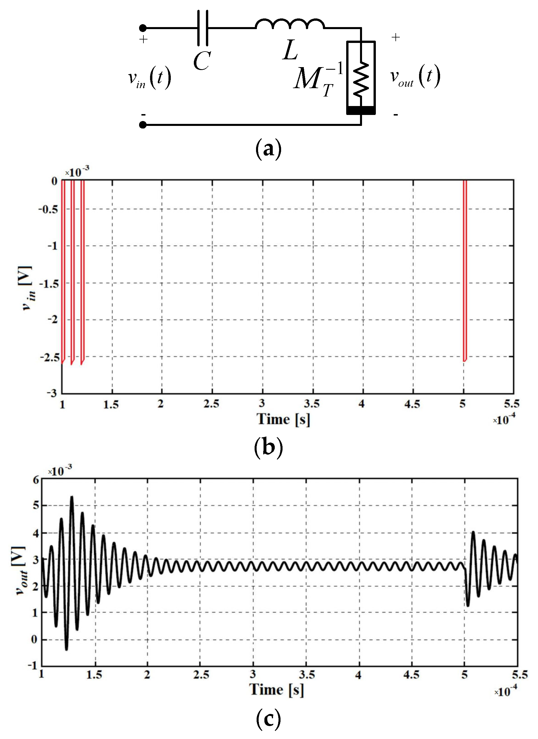
4.5. Application of Proposed Memtranstor Emulator in Adaptive Learning Circuit
The proposed memtranstor emulator is well suited for implementation in adaptive neuromorphic circuits and artificial neural networks [
4], where memory-dependent dynamics and history-aware learning are essential. An illustrative adaptive learning circuit employing the proposed emulator is shown in
Figure 11a, inspired by the experimentally observed learning behavior of
Physarum polycephalum (amoeba). In this biological system, the organism exhibits a gradual reduction in locomotion speed when exposed to repeated, periodic environmental stimuli, reflecting a primitive form of memory and temporal pattern recognition.
In the electronic analog, this adaptive behavior is emulated through the memtranstor’s intrinsic state-dependent response, which accumulates information about past excitations and modulates its dynamic state accordingly. The resulting circuit demonstrates the ability to encode temporal correlations and anticipate recurring stimuli without requiring complex digital control or explicit memory storage. Such bio-inspired adaptive functionality highlights the potential of the proposed memtranstor emulator for low-power learning circuits, neuromorphic sensory processing, and event-driven artificial intelligence systems.
In the proposed adaptive circuit, the input voltage emulates periodic environmental (e.g., temperature) stimuli, while the output voltage corresponds to the locomotive response of the amoeba. The memtranstive element continuously updates its internal state in response to the applied excitation, thereby modulating the effective circuit dynamics and enabling frequency-dependent adaptation. This state evolution effectively tunes the circuit to the temporal characteristics of the input stimulus.
Simulation results shown in
Figure 11c indicate that each excitation pulse produces a corresponding reduction in the output signal, analogous to a decrease in locomotive speed. Under repeated periodic stimulation, the response exhibits an initial transient followed by a gradual attenuation, reflecting habituation and anticipation of recurring events. In contrast, a single delayed pulse elicits a pronounced transient increase in the output, followed by rapid decay, consistent with stimulus-driven adaptation rather than sustained learning.
These observations demonstrate that the proposed memtranstor-based circuit successfully reproduces key features of biological adaptive learning, including temporal memory, stimulus anticipation, and history-dependent response modulation. The results further confirm the suitability of the proposed emulator for neuromorphic learning architectures and bio-inspired adaptive systems.
4.6. Comparasion with Exsisting MT Emulators
To assess the effectiveness and practical relevance of the proposed memtranstor (MT) emulator, a comparative evaluation against previously reported memtranstive and memristive emulator designs is presented in
Table 3. The comparison focuses on key performance metrics that are critical for neuromorphic and analog signal-processing applications, including circuit complexity, tunability, operating frequency range, power consumption, and implementation technology.
This comparative analysis highlights the advantages and trade-offs of the proposed architecture relative to existing solutions, thereby positioning the proposed emulator within the current state of the art and demonstrating its suitability for integration in adaptive and neuromorphic systems.
Based on the comparative evaluation summarized in
Table 3, several important observations can be drawn regarding the proposed memtranstor (MT) emulator.
Unlike several previously reported designs that rely on analog multipliers [
12,
13,
14,
24,
26], the proposed emulator employs a completely multiplier-free architecture, similar in principle to [
25]. Eliminating analog multipliers avoids associated non-idealities such as limited linearity, increased power consumption, and sensitivity to mismatch. As a result, the proposed design achieves a more compact, symmetric, and energy-efficient implementation with improved robustness and ease of integration.
The proposed configurations utilize only two active elements—one VDTA and one VDCC—leading to a significantly simplified circuit topology. This reduction in active building blocks directly translates into a lower transistor count, smaller silicon area, and improved power efficiency compared to existing implementations. Such simplicity is particularly advantageous for large-scale integration in neuromorphic and adaptive systems.
The emulator operates at a low supply voltage of ±0.9 V while supporting an operating frequency of up to 10,000 Hz, which is the highest reported among comparable memtranstor emulators [
12,
13,
14,
24,
25,
26]. Despite the reduced supply voltage and minimal circuit complexity, the proposed design maintains a wider usable frequency range, enabling improved dynamic response and broader applicability in real-time signal-processing scenarios.
The total power dissipation of the proposed emulator is only 0.76 mW, which is substantially lower than that reported in [
24,
25]. This low power consumption enhances suitability for energy-constrained environments, including portable, battery-powered, and IoT-oriented neuromorphic platforms.
The proposed emulator provides electronic tunability comparable to existing designs while offering additional flexibility through bias-controlled parameters. This feature enables dynamic reconfiguration of the memtranstive characteristics, making the circuit well suited for adaptive learning systems and reconfigurable analog architectures.
Memtranstors offer intrinsic non-volatile switching, parallel readout capability, and improved isolation compared to conventional memristors. These properties enable reduced power consumption and enhanced performance in data storage and signal-processing applications, approaching the functionality of traditional transistors [
9,
12,
29]. The proposed emulator supports both discrete two-state operation—suitable for non-volatile memory and logic circuits—and continuously tunable operation, enabling accurate emulation of artificial synapses for neuromorphic computing [
9,
30,
31,
32,
33].
Although the multiplier-free emulator reported in [
25] shares a conceptual similarity with the present work, several key distinctions are evident. The proposed design requires substantially fewer MOS transistors, resulting in reduced silicon area and fabrication cost. Moreover, it operates at a lower supply voltage and exhibits significantly lower power dissipation, thereby improving energy efficiency and operational autonomy. While an electronically controlled resistor (MRC) is employed to implement the required resistance, this is fundamental for enabling precise control of the memtransistor function. Importantly, by incorporating electronic tuning of the resistor value, we gain improved adjustability of the overall circuit performance—allowing optimization of linearity, frequency response, and dynamic range—without introducing an external multiplier or significantly increasing circuit complexity. This approach extends prior multiplier-free techniques in memristor emulators [
25]) to direct memtranstor emulation, providing a novel and practically controllable solution.
In addition, the proposed architecture exhibits reduced parasitic effects due to its simplified topology and grounded-capacitor configuration, leading to improved matching between active and passive elements. This contributes to enhanced stability, accuracy, and reproducibility of the emulated memtranstive behavior. The ability to maintain reliable operation up to approximately 10,000 Hz represents a notable improvement over previously published designs and is particularly beneficial for applications involving adaptive control, dynamic signal processing, and real-time emulation of nonlinear memory effects.
Compared to electrolyte-gated transistors (EGTs), the proposed MT emulator offers low-voltage operation (±0.9 V), high-speed response up to ~10,000 Hz, and compact CMOS integration using only two active blocks and minimal passive components. Its electronic tunability enables precise and reproducible control of LTP/LTD dynamics, while Monte Carlo and parasitic analyses confirm robust performance across process and temperature variations. These features make the MT emulator a more predictable, scalable, and integration-friendly platform for neuromorphic and analog memory applications than conventional EGT-based designs.
The dual ±0.9 V supplies maximize dynamic range and linearity, but standard on-chip solutions, such as charge pumps or level shifters, can generate the negative rail for single-supply operation. This ensures integration without modifying the core memtranstive behavior. Future work will investigate fully single-supply designs to simplify implementation while preserving adaptive-learning functionality.
The proposed memtranstor emulator reliably operates up to ~10,000 Hz, covering the typical range for neuromorphic and adaptive-learning circuits. While higher-frequency applications may require additional characterization, the VDTA/VDCC architecture is inherently scalable, allowing future extension of the bandwidth without fundamental redesign. This confirms both practical utility and design flexibility for real-time synaptic emulation.
From a broader design perspective, minimizing circuit complexity while preserving functional fidelity is a critical challenge in CMOS-integrated emulator circuits. Reducing transistor count not only decreases chip area and manufacturing cost but also improves yield and mitigates thermal and flicker noise contributions. Furthermore, low-voltage and low-power operation align with contemporary IC design trends emphasizing energy efficiency and scalability for embedded and neuromorphic systems.
While silicon measurements are not yet available, the proposed memtranstor emulator has been rigorously validated through pre- and post-layout simulations in 180 nm CMOS, including Monte Carlo and process-corner analyses. These simulations confirm robust pinched hysteresis behavior, low-power operation, and resilience to variability and parasitics, providing high predictive confidence for real-world implementation. The results demonstrate the emulator’s suitability for adaptive learning circuits and neuromorphic applications without requiring complex analog multipliers.
Post-layout simulations reveal minor PHL deviations, particularly in the third quadrant, which were quantified using normalized loop area and symmetry metrics: loop area changes were computed as the fractional difference between pre- and post-layout hysteresis, while asymmetry factors were calculated from the ratio of positive to negative lobe amplitudes. Across these variations, memtranstive behavior remains robust, with minimal impact on effective memory states. Temperature- and time-dependent analyses, performed via extended PVT sweeps from −27 °C to 100 °C and retention simulations up to 104 s, confirm that memtranstance drift remains below 10%, demonstrating strong stability under realistic operating conditions. The VDTA and VDCC are realized using fully CMOS-compatible differential pair topologies (18 and 22 MOSFETs, respectively) in 180 nm technology at ±0.9 V, with careful transistor sizing and biasing ensuring reproducibility across process corners and mitigating parasitic effects. Collectively, these results validate the emulator’s functional integrity, robustness to layout, temperature, and long-term drift, and feasibility for standard CMOS integration, providing confidence for neuromorphic and nonlinear analog applications.
Overall, the proposed memtranstor emulator achieves a balanced combination of architectural simplicity, low power consumption, wide operating frequency range, and electronic tunability. Monte Carlo analysis, process-corner evaluation, experimental verifications and post-layout simulations confirm robust operation across manufacturing variations. The elimination of strict component matching requirements further enhances practical feasibility.
Finally, the versatility of the proposed emulator is demonstrated through its applicability in a variety of analog and unconventional computing circuits. Replacing conventional resistors in RC networks with the proposed memtranstor enables electronically tunable low-pass, high-pass, band-pass, and band-reject filters, as well as BPF-based oscillators, Colpitts chaotic oscillators, and Schmitt trigger circuits. Additionally, successful implementation of an OR–AND logic gate highlights the emulator’s potential for non-von-Neumann and neuromorphic logic applications.