

Article

Additive Manufacturing for Electronics (AME): Prototyping High Surface Area Substrates to Improve Thermal Performance


1
Chilab-ITEM Laboratory, Department of Applied Science and Technology (DISAT), Politecnico di Torino, Via Lungo Piazza d’Armi 6, Chivasso, 10034 Turin, Italy
2
Microla Optoelectronics S.r.l., Per Via Gozzano 34, Chivasso, 10034 Turin, Italy
*
Author to whom correspondence should be addressed.
Electronics 2026, 15(5), 1002; https://doi.org/10.3390/electronics15051002
Submission received: 30 January 2026 / Revised: 23 February 2026 / Accepted: 25 February 2026 / Published: 28 February 2026

Abstract

Nowadays, Additive Manufacturing for Electronics (AME) is gaining ground in device fabrication for the numerous advantages of these types of manufacturing technologies, such as fast production processes, freeform design, and low-cost prototyping. In this scenario, the proposed research work is focused on evaluating an innovative strategy for a common issue in power electronics, which is related to the generation of hotspots. To face this problem, the 3D printing of ceramic substrates with different high surface areas was studied to improve thermal dissipation. Together with improved thermal management, the upper surface of the devices enabled the deposition of a desired conductive pattern and the bonding of bare die components for device fabrication. Finally, thermal exchange was monitored to verify the efficacy and efficiency of the devices’ dissipation capabilities. The proposed models exhibited a 70% temperature reduction upon transitioning from air to water. Furthermore, the operating temperature remained stable for 10 min, meeting the specific requirements of the intended application.

1. Introduction

The global effort to reduce greenhouse gas emissions, as part of the climate change mitigation strategy, is pushing towards more sustainable and renewable energy sources [1]. In this direction, the automotive industry is experiencing a global change from traditional fossil fuels towards Electric Vehicles (EVs). This shift requires high-performance electronics and energy storage systems to satisfy the transportation needs [2]. In addition, the Artificial Intelligence (AI) revolution requires ever more powerful and dedicated Data Centers. Within this frame, the power electronic industry is facing a rapid increase in demand for smaller, faster, and more efficient power converters [3].

1.1. Thermal Management of Wide Bandgap Devices

As a solution to the increase in power density and switching frequency, in many applications, wide bandgap (WBG) materials are today employed as semiconductors. Unlike traditional silicon (Si), which has a bandgap of approximately 1.1 eV, WBG materials have bandgaps in the range of 3.2 to 3.4 eV. This physical property allows these materials to withstand much higher electric fields, operate at higher temperatures, and switch at significantly faster speeds. Wide bandgap materials like silicon carbide (SiC) and gallium nitride (GaN) are becoming extensively employed whenever high power or high switching frequency are required [4]. In particular, GaN devices are characterised by a smaller specific ON-resistance and switching losses. These properties are crucial for high-frequency and high-power-density converters. To be fully exploited, however, WBG requires packaging solutions that can boost the electrical and thermal performances [5,6].
Especially concerning power dissipation, many solutions have been developed for reducing the thermal resistance of the substrate or introducing innovative cooling mechanisms. As far as the substrate is concerned, Printed Circuit Board (PCB) has been proven many times to lower the inductances, but at the same time, they cannot reduce the thermal resistance significantly without a further level of integration [7,8]. However, other substrates like Insulated Metal Substrate (IMS) and Direct Bonded Copper (DBC) are characterised by very low thermal resistance [9,10], but their 2D structure only allows some planar configurations, generating higher critical inductances [5]. In addition to that, the third dimension has also been exploited for power dissipation. For example, the double-sided cooling architecture allows for doubling the effort despite increasing the cost and the overall volume of the module.

1.2. Liquid Cooling Systems

Traditional cooling strategies and common coolants are no longer sufficient to manage the elevated heat generation encountered in modern semiconductor technologies. As a result, next-generation high-performance devices require advanced thermal-management concepts that can be integrated directly into emerging packaging architectures. This progression involves innovations in materials, structural design, and the adoption of specialized cooling liquids capable of providing substantially higher heat-removal capability.
Cooling systems can be classified according to several criteria, mostly based on the thermophysical and electrical properties of the working fluids/gases or on their functional role within an advanced packaging architecture. In fact, the first widely used criterion concerns the cooling medium employed. Based on this, cooling systems are typically classified as either air- or liquid-cooled architectures. Air-cooled systems rely on airflow, naturally or forced, to remove heat, while liquid-cooled systems use circulating fluids with higher thermal capacity to achieve more efficient heat extraction, enhancing the levels of integration and major reductions in the volume and weight of power electronics systems.
Another of the most common approaches focuses on their operating principle, distinguishing passive from active systems. Passive systems operate without the need for external energy input, whereas active systems rely on additional energy to drive components such as fans, pumps, or thermoelectric modules [11].
Further classification is based on the presence or absence of a phase change in the working fluid. When this criterion is applied, cooling systems can be divided into single-phase and two-phase systems. Single-phase cooling maintains the working fluid in the same state throughout the heat-transfer process, relying solely on sensible heat exchange, which implies a limited cooling effect due to relatively low heat transfer coefficients (<2 kW/(m2 K)) [12]. Nevertheless, recent studies have demonstrated that advanced designs can significantly enhance single-phase liquid performance. For example, an embedded micro-manifold cooling (EMMCs) SiC power module employed crossed double-layer liquid distribution and identical cooling paths beneath each chip, achieving highly uniform cooling. This design enabled single-phase heat dissipation of up to 655 W at a mass flow rate of 3 g s−1 with a maximum temperature rise of 60 K, compared with 370 W for a conventional pin-fin–cooled module [13]. Two-phase systems, by contrast, involve phase transitions such as boiling or condensation, enabling the absorption or release of large amounts of latent heat. This mechanism can significantly increase heat-removal efficiency and allows the design of compact, high-performance thermal management solutions [14,15]. However, two-phase cooling is more complex than single-phase cooling, involving limited understanding of characteristics and instabilities, like flow boiling suffers from hydrodynamic instabilities [16,17].
Regardless of the phase selected for the cooling fluid, liquid-based cooling solutions can be integrated directly into the device packaging through various geometrical configurations, such as microfluidic channels, pin-fin structures, or other engineered pathways, thus enabling direct-contact cooling of the dies. Within this class of designs, the heatsink may be applied to a single side of the electronic die (single-side cooling) or to both sides (double-side cooling), depending on the thermal requirements and packaging constraints. Overall, double-sided cooling strategies provide superior electrical and thermal performance. Compared with single-sided cooling, double-sided cooled power modules exhibit up to a 50% reduction in device-to-coolant thermal resistance, resulting in a significant decrease in junction temperature [18].
Alternatively, the cooling system may rely on immersion cooling, in which the entire PCB together with its electronic components is submerged in a tank filled with a dielectric coolant. This approach provides uniform convective heat removal and can significantly enhance thermal performance, especially in high-power or densely integrated electronic systems.
The selection of an appropriate cooling liquid for electronic devices and power modules depends on several interacting factors, including allowable electrical conductivity, required heat flux removal, system packaging, and long-term reliability constraints. Deionized water and water–glycol mixtures remain the most effective fluids in terms of thermal conductivity and heat capacity; in particular, they are widely used in closed-loop liquid-cooling systems, although their electrical conductivity limits direct contact with electronic components [19]. Non-conductive dielectric liquids, including mineral and synthetic oils, silicone oils, and engineered fluorocarbon fluids such as Novec™ or Fluorinert™, enable single- or two-phase direct immersion cooling but exhibit lower thermal performance and, in some cases, higher cost and environmental impact. In fact, these fluids exhibit several key limitations. First, the low boiling point of non-polar dielectric liquids at atmospheric pressure restricts allowable component temperatures, as vapor-blanket formation near ≈50 °C rapidly triggers critical heat flux. Second, the maximum removable heat flux is limited by the fluid’s critical heat flux, which for typical dielectric liquids (<20 W cm−2) falls well below the requirements of emerging high–power-density electronics (>100 W cm−2). Third, dielectric liquids possess comparatively poor thermophysical properties, including lower thermal conductivity, latent heat, and surface tension—relative to ideal conductive fluids such as water [20]. Alternative bio-based esters and silicone-based fluids offer improved biodegradability or stability, while emerging nanofluids provide enhanced thermal conductivity at the expense of increased complexity and potential stability issues. Various types of nanoparticles have been explored for the preparation of nanofluids intended for liquid-cooling applications, with metal-oxide nanoparticles representing the most widely employed class of additives in this domain [21].

Fundamental Configurations and Variants of Heatsink Design

Regardless of the chosen design architecture, the most vital part of these devices is linked to the thermal resistance of the heatsink, which can be expressed using the following relation (1) widely adopted in heat-exchanger design literature:
R s a =   1 m ˙ c p 1 e h A m ˙ c p
The thermal performance of liquid-cooled heatsinks is governed by several design parameters, among which the internal geometry and flow-channel configuration play a particularly critical role in shaping fluid distribution and determining overall heat-transfer effectiveness [22,23]. According to the general thermal-resistance relation, performance can be enhanced by increasing the mass flow rate m ˙ of the coolant—typically through forced rather than natural convection—by selecting a working fluid with higher specific heat capacity c p (e.g., liquids instead of gases), and by raising the convective heat-transfer coefficient h at the solid–fluid interface. The latter can be improved through reduced channel dimensions such as microchannels, the promotion of turbulence via flow disruptors or boundary-layer interruption, and the use of two-phase mechanisms (evaporation and condensation) instead of single-phase convection. In addition, the effective heat-transfer area A , defined as the surface area in contact with the coolant multiplied by its fin or surface efficiency, is the last critical factor.
A typical liquid-cooled heatsink consists of an inlet manifold, an outlet manifold, and a central region containing the engineered flow passages. Based on the arrangement of these passages, liquid-cooled heat sinks can be grouped into three primary categories: parallel-channel structures, pin-fin architectures, and more complex hybrid geometries [24,25].
Parallel straight-channel designs remain the most conventional and widely adopted configuration, consisting of multiple linear channels arranged in parallel and separated by thin walls. Numerous geometric variants—including wavy or serpentine channels, ribbed passages, and cavity-enhanced designs—have been developed to intensify local mixing [26,27,28]. These features promote secondary flows, recirculation zones, and vortical structures that disrupt thermal boundary-layer development and thereby enhance convective heat transfer. However, such improvements generally increase pressure drop and pumping power requirements. Consequently, extensive research has focused on optimizing the size, shape, and distribution of enhancement elements such as ribs, cavities, protrusions, and obstacles to achieve improved thermo-hydraulic performance while maintaining acceptable flow resistance.
However, several research gaps and challenges remain in heat-sink design, especially due to multiple-peak heat fluxes, which are common in modern electronics but have been insufficiently addressed. Most existing designs still assume uniform heating, which poorly reflects real operating conditions. Future studies should emphasize non-uniform thermal loads and develop design guidelines specifically for cooling surfaces with multiple heat sources.

1.3. Additive Manufacturing for Electronics and Industry 4.0

Looking at the full picture, thermal management of power electronics was invested in by the novelty of the fourth industrial revolution, as in all production fields.
The term 4th revolution involves cyber-physical systems, which means the Internet of Things and services for interconnecting both devices and people globally, and for merging the real and cyber worlds. The consequential result of this process was represented by smart factories, which presented decentralized manufacturing approaches accomplished by means of intelligent production systems, vertically and horizontally integrated for a consistent value chain [29]. Part of this evolution was the introduction of additive manufacturing (AM) technologies not only for part prototyping, but also for final component fabrication.
AM technologies spread fast in the manufacturing industry, substituting traditional fabrication processes in some niches that needed high mass customization. However, more and more fields are asking for shorter lead time and greater personalization, which means flexibility, adaptability, and stability of the products, as well as more sustainable approaches in fabricating parts, so AM processes could address these requirements [30]. Introducing AM in Industry 4.0 opened up to multifunctional structures, made of different classes and combinations of materials, which allowed the manufacturers to reduce the time-to-market, to automate the manufacturing and repairing processes, to develop new complex components on demand, overcoming some traditional limitations in terms of tools needed and assembly processes [31]. Together with the mentioned points, another pushing theme for AM introduction as Industry 4.0 aid is the possibility of performing a light-weighting of the parts. This process involves the reduction of required material for fabricating the final object, reaching better performances at the same time. It is strictly correlated with the concept of topology optimizations of complex structures, that show inner frameworks with intricated geometries. These complicated shapes can be easily modified and fast produced, meeting the continuous feedback from the final customers who are included in the production cycle. This design approach, called design intelligence, reduces manufacturing costs and wastes, supports implant decentralization, reducing plant duplication and downtime [30]. Because of the above-mentioned points, the electronics sector expressed a degree of interest in AM technologies for device fabrication, leading to the advent of 3D printed electronics, which is the pairing of AM technologies and components integration and/or direct manufacturing of electrically conductive paths. The fully 3D printed electronics approach, also known as additively manufactured electronics (AME), contemplates the deposition layer by layer of a multilayer 3D circuitry, even with complex geometries [32]. Nevertheless, producing these complicated devices structures through AME, meeting the needs for Industry 4.0 at the same time, requires the use of supporting technologies, mainly software. Normally, AM technologies always ask for CAD software for designing the printed parts and the additional elements as support structures and so on. After that, the 3D model is translated into an outer surface shell, namely the .STL file (Standard Tessellation Language). Lastly, this file is sliced into its constitutive single layers, whose number depends on the selected layer thickness for the chosen technology and required resolution [33].
Considering the advent of automation and the continuous feedback provided by the customers in the Industry 4.0 scenario, CAD modelling is no longer sufficient to satisfy the increasing demand for closed-loop manufacturing and the need for maintaining low consumption of materials and resources, without affecting final properties. This is the reason why the new “Digital Twin” concept was introduced in AM, and notably in AME. This term comprehends the creation of a virtual model of the final parts/objects or processes, which are used for high-fidelity simulations and modelling. Virtual models can improve decision-making and optimization processes both for design and manufacturing phases, making digital twins of AME products a high-potential strategy to monitor, diagnose, and control manufacturing processes [34,35].
Digital twins can be used in a variety of applications, such as to locate and correct possible defects, provide real-time state-of-health, and anticipate failures. In the electronics field, digital twins can be used to supersede the use of physical validation prototypes, which can be extremely costly [36]. Virtual cooling analysis is one application that is of particular interest in the power modules field, since it can be used together with practical experiments to design physical cooling systems. In this sense, digital twins can be used to study the effects that different coolants, flow rates, and geometries have on the effectiveness of the system before using the gathered data to develop a physical prototype [35,37].

1.4. Aim of the Research Work

Looking at the growing interest in novel semiconductors for the innovative application fields of electronic devices, new cooling strategies are crucial for a correct thermal management of the developed systems. Liquid-cooled devices represent an interesting and functional solution for determining high heat exchanges in newly developed devices for different sectors, especially for high-power applications. High switching frequencies and power requirements demands can be faced by GaN devices, which need cooling strategies able to extract the high level of generated heat from the deputed connection pads.
This was the rationale behind the following presented work, whose aim was to develop an alternative ceramic substrate for a GaN die, with a complex 3D geometry that guaranteed a large heat exchange area for liquid cooling and a flat planar 2D surface for metallization and die attach. The complex design, presenting the bonding plane on one side and the intricate geometry on the other, was first adjusted based on the multiphysics simulation, and then manufactured additively in alumina as a ceramic material. To fabricate the heat exchange platform, a Vat PhotoPolymerization (VPP) technique, namely Digital Light Processing (DLP), was chosen because of its high resolution, with an achievable minimum feature size of 50 μm, good accuracy and precision, excellent surface quality, and faster printing time, with a high throughput [38,39]. This vat-based technology involves the use of a reservoir filled with photocurable resin, in which a build platform moves along the Z-axis to recover the growing piece with a fresh layer of resin. Each of these layers is photopolymerized by a projector that typically works in the UV/near-UV range, projecting a pattern mask generated by a digital micromirror device. The micromirrors represent all the available pixels, switched between on and off stage for obtaining the desired geometry [38,39,40]. For depositing the conductive path needed for the component’s soldering, an extrusion-based (MEX) printer was selected. In these types of AME techniques, such as Direct Ink Writing (DIW), inks are deposited on a substrate using a syringe or container and a pressing piston, whose pressure can be regulated by a screw. This technology is frequently chosen because it doesn’t require a heated printing head or bed. However, rheological requirements for the printable inks are strict, due to the necessity for high consistency and gel-like viscosity, for ensuring the proper shape retention after the ink deposition [41]. In this study, the conductive inks were deposited using a MEX electronic prototyping tool for the design of printed circuit boards (PCBs), equipped with software that translates a Gerber file, which contains the design of the circuit, into precise instructions [42]. Later, the GaN component was soldered on the deposited silver pad, through the thermal pad, and connected to the testing circuitry, used for the thermal exchange evaluation. Lastly, thermal characterization was performed, using a thermal camera for registering the heat flux, a hydraulic system for providing liquid coolant, namely water, into the 3D printed substrate, which was fixed into a 3D printed chamber for liquid containment.
In this context, three different models were designed, simulated, fabricated, and tested, showing that the digital model and the real world had a close agreement in terms of experimental and simulated thermal behavior. In detail, all the designed parts could achieve efficient thermal exchange with the selected cooling medium, compared to solely air cooling, demonstrating the importance of large exchange areas on electronic substrates for high switching devices.

2. Materials and Methods

Three different substrate configurations were designed, simulated, and fabricated in this work, while the hydraulic system was adapted for the various solutions. Each configuration is composed of the heat exchange platform and a custom-built holder, and it differs from the others in the heat transfer fins pattern.
The GaN component selected for performing some first trials in terms of heat dissipation, die attaching, and simulation was the Top-side cooled 100 V E-mode GaN transistor (GS61008T, Infineon Technologies AG, Neubiberg, Germany). This specific component was chosen since it has a big thermal pad located on the back with respect to the power and gate terminal region. This thermal pad has a low thermal resistance, 0.55 K/W, and it is located very close to the active part of the component [43].

2.1. Design and Simulation

Finite-Element-Method (FEM) simulations were used to determine the most performing design out of the three configurations. Five simulations were conducted in COMSOL Multiphysics 6.4, each employing one of the three different model designs. The study was set to couple the Fluid Dynamics and Heat Transfer modules through the Multiphysics interface. For each simulation, results were gathered regarding the temperature of the body and the velocity field of the water flow. The aim of the study was to determine which of the heat transfer fin patterns is more suitable for the heat exchange platform, by considering the pattern that leads to a lower overall temperature of the body.
The five simulations were employed to assess the viability of the system. By simulating the model, it was possible to verify that the system was effectively working as intended before printing it. The simulations were set as follows: the first three simulations each employed one of the three models; a fourth one employed model 1 with the addition of a box of air surrounding it; a fifth simulation was created with model 1 without water to be used as a comparison for a no-flow state. The box in the fourth simulation increased the similarity with a real case scenario, and it was used to detect possible differences with the simpler but less realistic no-box simulations, for thermal data comparison only. The four simulations without an air box were built with an air flux node on the external boundaries of the model to simulate the surrounding environment.
The 3D CAD models designed and simulated for each of the three configurations are reported in Figure 1. The three models are each comprised of the holder, the alumina heat sink, and a replica die composed of four layers of acrylic plastic, GaN, silicon, and gold to mimic the exact anisotropic thermal behaviour of the component and its thermal pad. The replica die reflected the same dimensions of the real die, having a volume of 7 mm × 4 mm × 0.65 mm. The holders for the three models differ in the cavity volume in order to accommodate the different heat sinks, which have different dimensions. Holder for model 1 has cavity dimensions of 14.7 mm × 10.7 mm × 8.2 mm, for model 2 19.7 mm × 10.7 mm × 8.2 mm, and for model 3 20.78 mm × 10.7 mm × 8.2 mm (width, depth, height, in mm).
For each simulation, a domain heat source was placed on the active layer of the component and set to have a heat rate of 1.4 W. For the four simulations with a water flow, water was set to flow through the inlet and into the chamber at 16 °C with a flow rate of 17.3 mL/min. Power was calculated according to
P = I V
where the electric current I = 140 mA and the V = 10 V. The flow rate was set as to be the same value of the pump used in the test phase.
The following materials were assigned in the model builder: acrylic plastic for the holder and for the upper half of the component; air for the air box surrounding the system; alumina for the heat exchanger; gold for the die thermal pad; silicon for the lower half of the die; silver for the silver layer laid down on the heat exchanger; solder paste for the solder paste layer spread onto the silver layer; water for the coolant; GaN for the gallium nitride layer inside the component. Material properties used in the simulations are reported in Table 1. For alumina, values given by COMSOL documentation were used for heat capacity, while density and thermal conductivity were taken from the alumina manufacturer’s database. Simulation results proved to be consistent with thermal tests.
Stationary Navier-Stokes equations were used to evaluate the fluid dynamics simulations, assuming the fluid to be incompressible and Newtonian so that density and viscosity could be approximated as constants. The no-slip boundary condition was applied on the exterior walls [47]. For the Fluid Dynamics part of the simulation, water was set to flow from the inlet surface as a fully developed flow with a fixed flow rate. Laminar Flow and Heat Transfer were coupled within the COMSOL interface to study the heat dissipation effectiveness of the system.
The mesh was generated in two steps by building the GaN layer first and the remaining domains last. This was done to ensure that the mesh building process properly considered the different dimensional scales of the domains, since the GaN layer had a thickness of 1.5 µm.

2.2. AME

The simulated substrates were 3D printed using AdmaPrint A130 (Admatec, Goirle, The Netherlands) as constitutive material and the Admaflex 130 Entry (Admatec, Goirle, The Netherlands) as DLP printer.
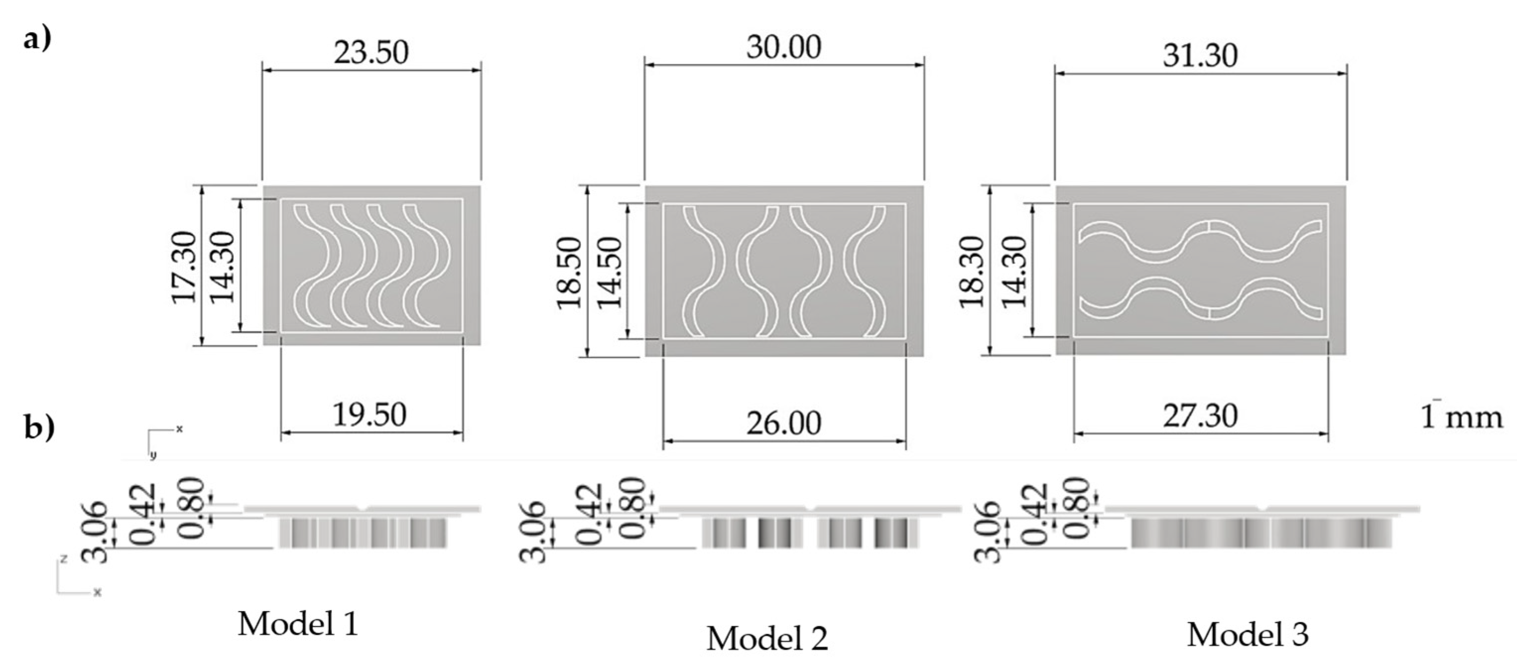
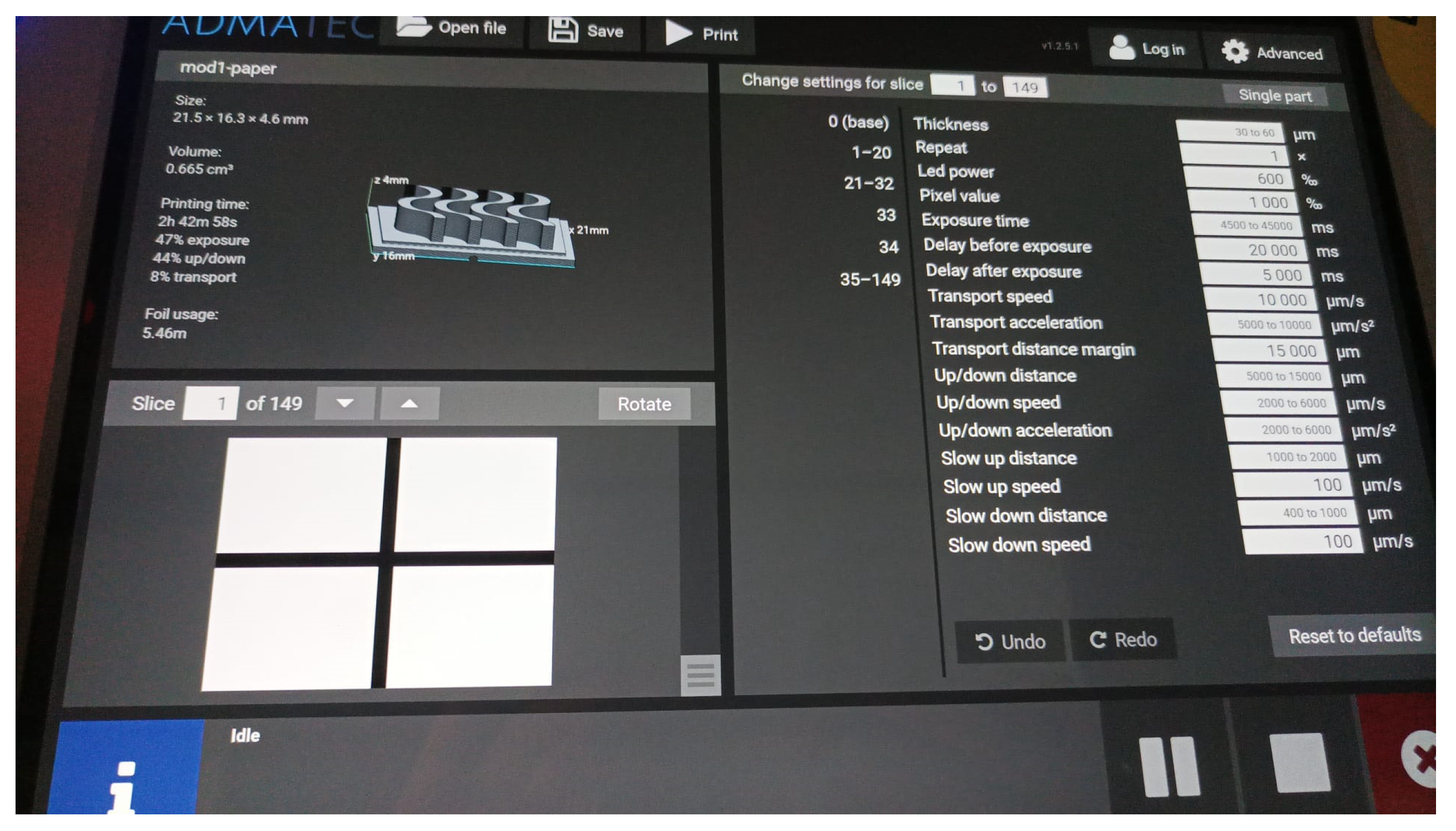
For ensuring good build platform adhesion during printing, a baseplate was designed and added to the CAD models, generated using Rhino 5.0 (Robert McNeel & Associates, Washington, DC, USA) as reported in the Figure 2 below, together with the printed dimensions adapted of 1.3× along X- and Y-axes, and 1.39× along Z-axis, for compensation for sintering shrinkage. The used parameters, set for each slice generated by the printer software (AdmaflexUI v1.2.5.1, Admatec, Goirle, The Netherlands) (Figure 3), are summarized in Table 2 below.
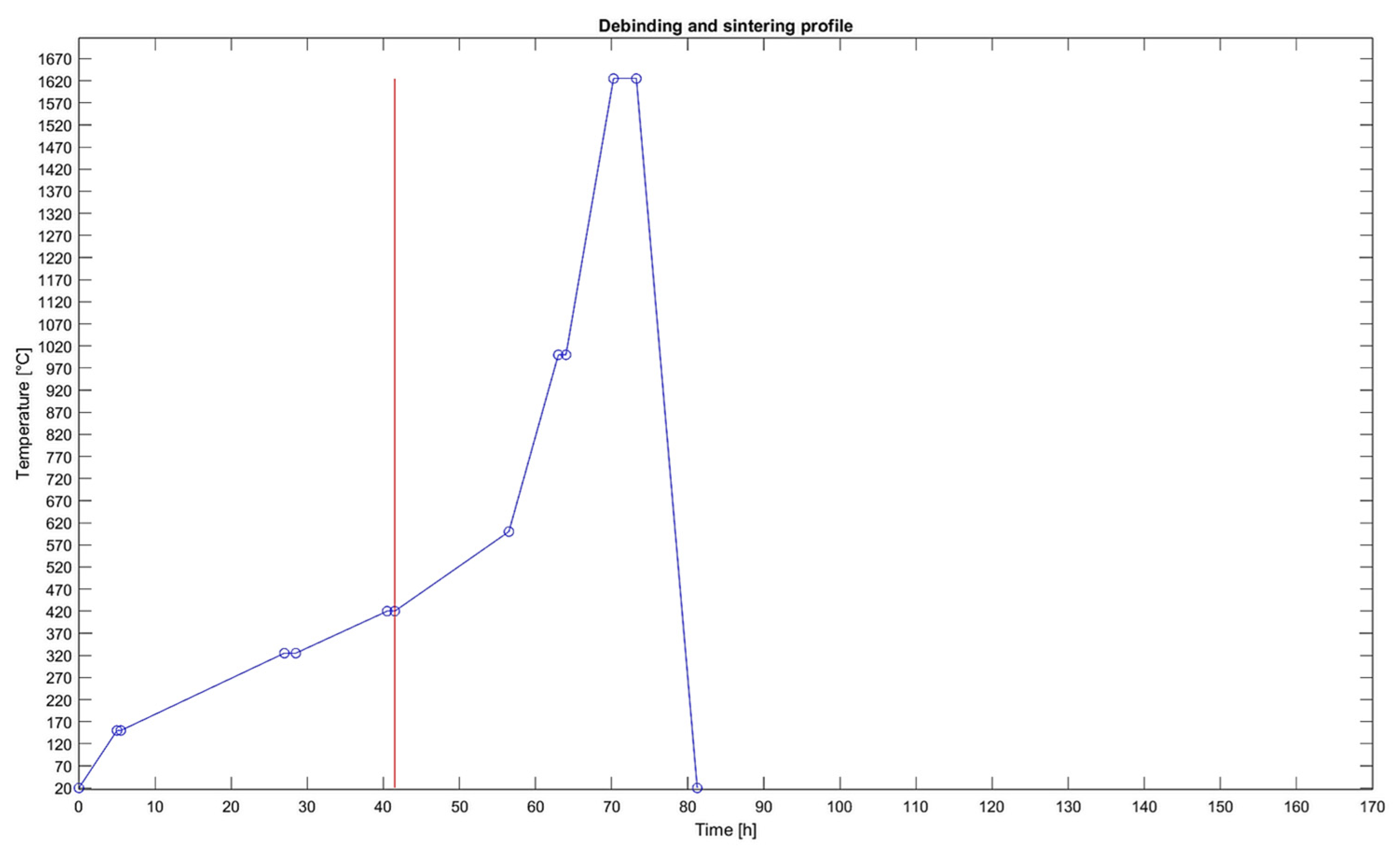
After printing, the parts were cleaned using Tri (propylene glycol) monomethyl ether (TPM) as wash solvent (3D basics, AprintPro, Guntramsdorf, Niederosterreich, Austria) and ultrasonic bath (CP104 ultrasonic cleaner, CEIA, Arezzo, Italy) for 5 min at 59 kHz. Lastly, the thermal debinding and sintering were performed to obtain the final white objects. The processes were carried out through the furnace (Bottom loading debinding/sintering furnace, Termolab, Agueda, Portugal), using the profile reported in Figure 4.
The conductive pads were printed on the sintered alumina substrates with the MEX printer Voltera V-one (Voltera Inc., Waterloo, ON, Canada). The used conductor ink was Conductor 3, which is a silver-based ink provided by the machine’s manufacturer (Voltera Inc., Waterloo, ON, Canada). This type of ink was chosen because of its high conductivity and stable performance in ambient conditions [48,49]. The selected extrusion nozzle inner diameter was 0.23 +/− 0.01 mm, and it was used to print a pad with XY-dimensions of 3.1 × 5.5 +/− 0.2 mm. The deposition parameters were print height Z = 0.03 mm and extrusion rate E = 5 µm. After depositing the ink, the curing process was performed to solidify the ink and ensure adhesion to the substrate. The chosen profile was 90 °C for 45 min during the curing process in the oven (UF30, Memmert GmbH+, Schwabach, Germany).
Additive manufacturing techniques were also employed to create the holder for the heat exchanger. The holder was comprised of a bottom part, which included the inlet and outlet for the tubes, and a vat to insert the heat exchanger into. The CAD design was created using Solidworks 2024 and then printed using the OBJET30 Polyjet printer from Stratasys (Eden Prairie, MN, USA). This 3D printer uses a liquid UV photopolymer as resin (VeroWhiteTM, Stratasys, MN, USA), deposited by the inkjet head layer by layer. Each layer is polymerized by the UV lamp, and after each layer is completed, the tray steps down along the Z axis to start over with another deposition. Along with the photopolymeric resin mentioned, the printing head deposits another material, the SUP705 sacrificial support, that was removed immediately after the printing phase.

2.3. Component Attach

The component was attached to the heat exchanger pad using a eutectic die-attach process. For this purpose, the Sn42Bi57Ag1 Low Temperature Solder Paste (MG Chemicals, Burlington, ON, Canada) was used. The solder paste was applied as follows: first, the paste was deposited on a small spatula directly from its syringe, then the paste was manually spread on top of the silver layer. A stencil made from a sheet of Kapton with a thickness of 75 µm and XY dimensions of 3.1 × 5.5 mm was used to confine the paste and to control its thickness.
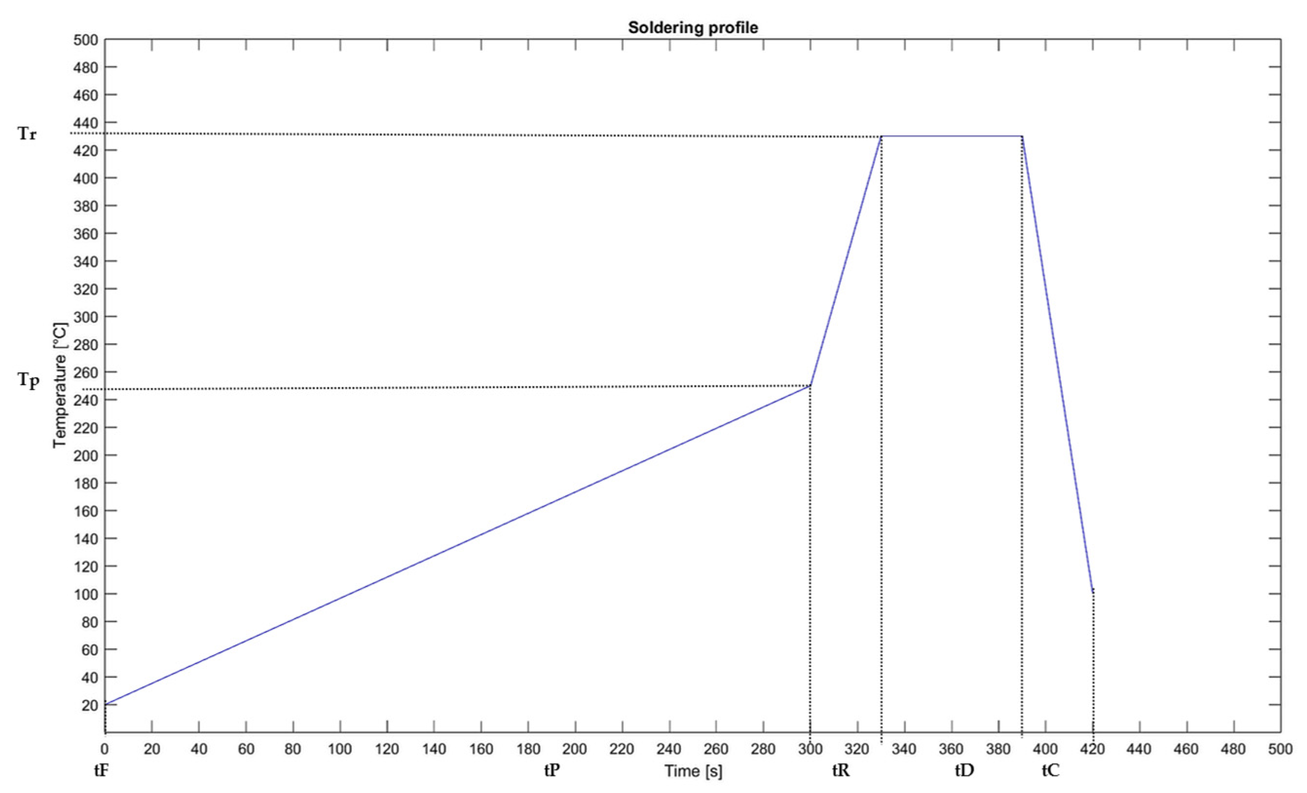
After positioning the component on the solder paste layer, the device was put into the MR10 reflow oven (Mechatronika sp.j., Elbląg, Poland) with the soldering profile reported in Figure 5. The set parameters, reported in Figure 5, were Tp (preheating heater temperature), Tr (reflow heater temperature), tF (initial preheating time), tP (preheating time), tR (reflow time), tD (dwell time), and tC (cooling time).

2.4. Testing

The thermal performance of the developed prototype equipped with the innovative heatsink was evaluated using an infrared camera SC240N (Vevor, Shanghai, China) (thermal range: −20 °C to +350 °C; resolution: 240 × 180 pixels; framerate: 20 Hz). The prototype was mounted on an optical test bench under standard operating conditions, and the camera was positioned to capture the full surface under test. Thermal images were recorded during operation until steady-state conditions were reached, with temperature profiles analysed to extract maximum and minimum temperatures, as well as the temperature at the point of interest.
For creating the closed-loop recirculation system, polyurethane tubes and a peristaltic pump were used. The tubes (TU0604G-20, from SMC, Tokyo, Japan) were 16 cm long, both for the inlet and outlet of the system, and were directly mounted on the container through a push fit. The peristaltic pump (Fluid-o-Tech, TP16, Milan, Italy) was then connected to the tubes and set at 16 V, which corresponded to a measured flow of 17.3 mL/min. The selected cooling liquid was distilled water at 16 °C, which was introduced into the system through the vat.
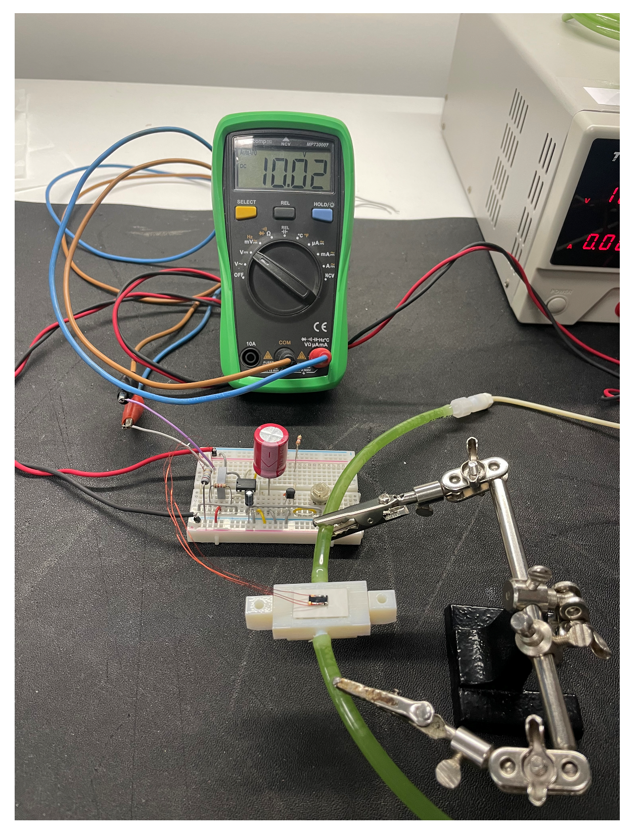
The GaN device was turned on and heated up by connecting it to a conditioning circuit, designed for generating about 1.4 W at 10 V. The power supply Tenma 72-2645, Triple Channel DC Power Supply, Programmable, 315 W (Chinese Original Equipment Manufacturers (OEMs) Zhongshan City, Guangdong Province, China) was connected to the device using copper wires with tinned ends (Figure 6).

3. Results

3.1. Design and Simulation

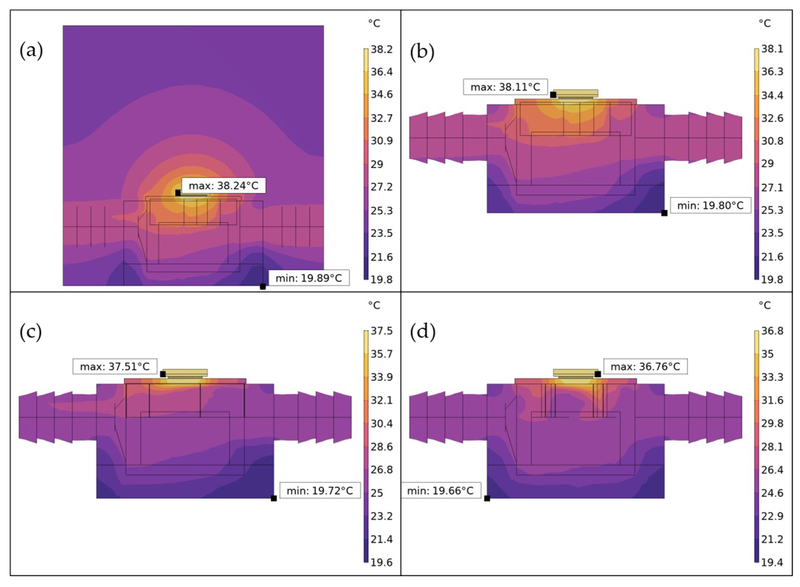
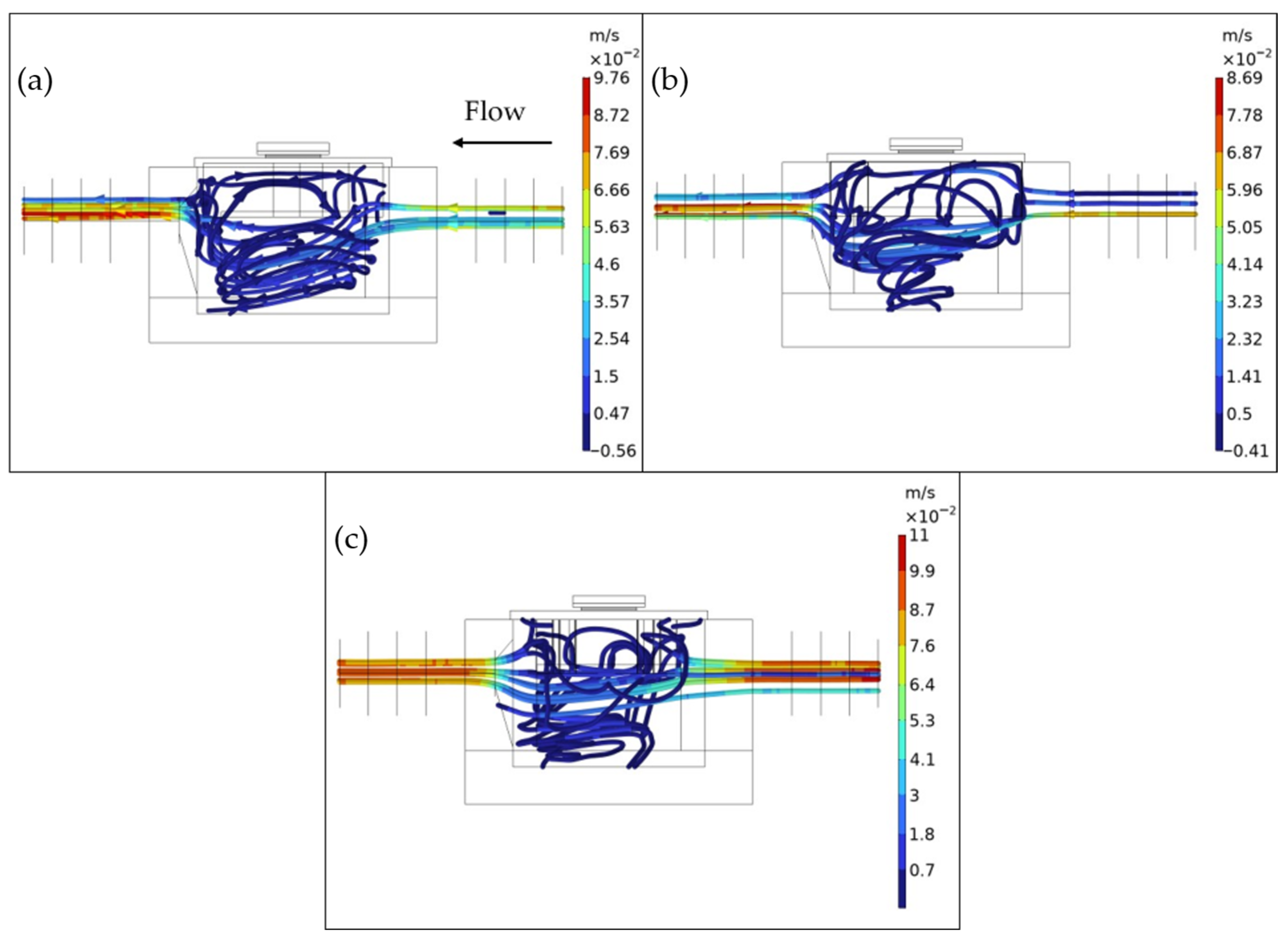
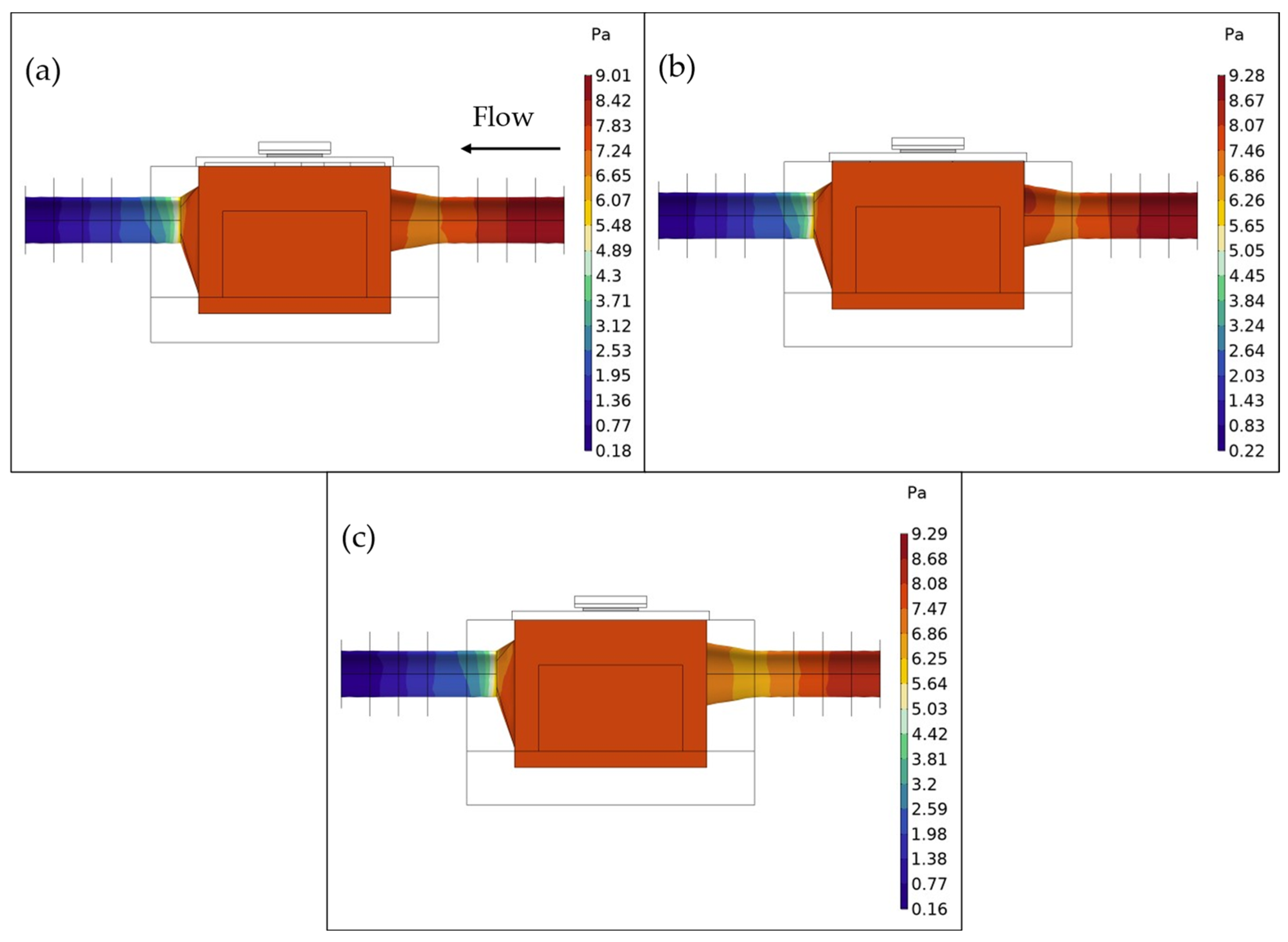
The temperature, velocity field, and pressure results are reported in Figure 7, Figure 8 and Figure 9 respectively. As can be seen in Figure 7, simulating an air box surrounding the model didn’t contribute significantly to the temperature results, with respect to the simulations without it. Overall, there is a negligible difference between the three designs employed. The simulated model 3 gave overall lower temperatures compared to the others, with slightly higher velocity and pressure.
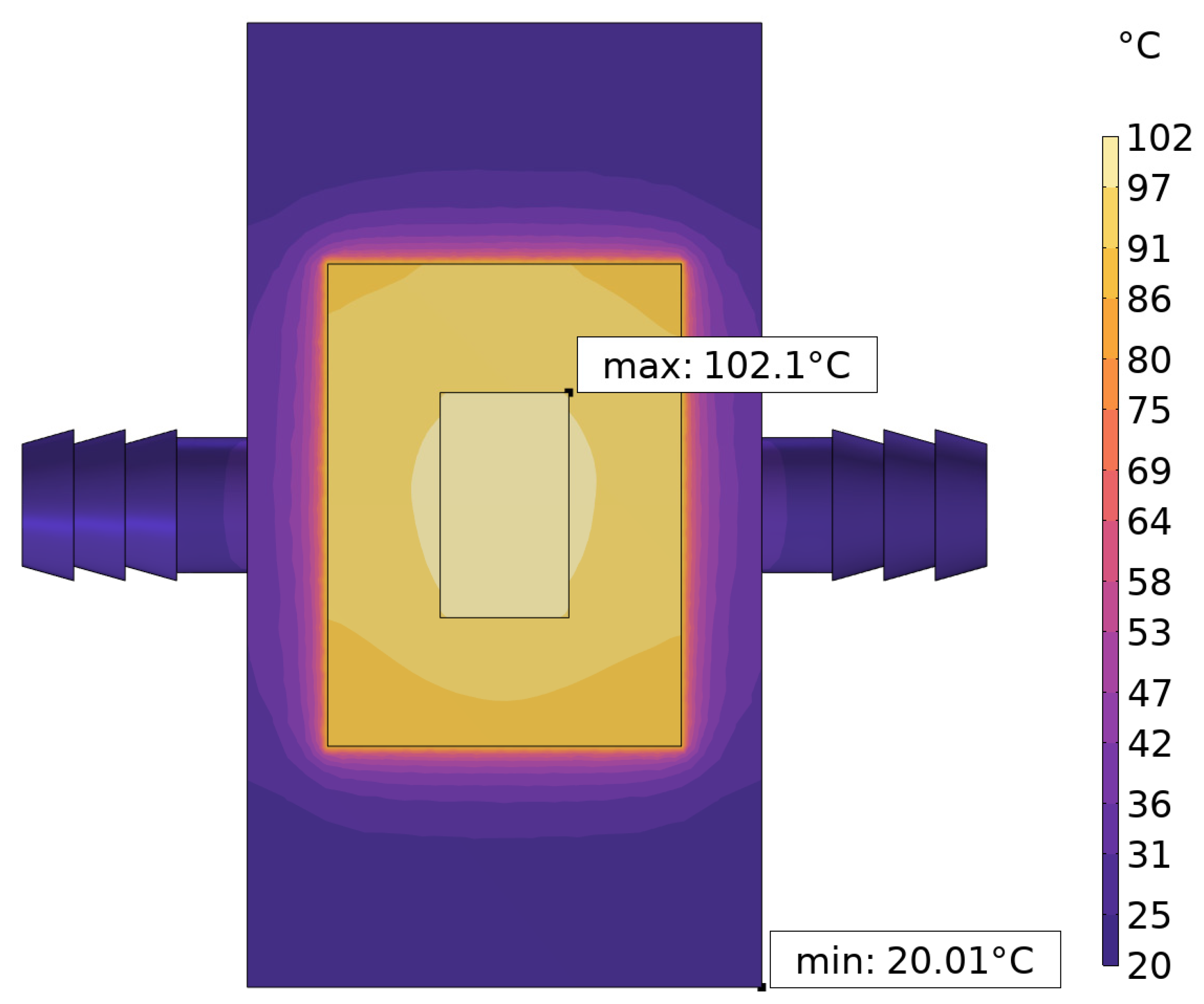
For comparison purposes with a no-flow scenario, results for the simulation with model 1 without water flow can be seen in Figure 10.
The three different models were tested with respect to their thermal resistance and convective heat transfer coefficient.

3.2. AME

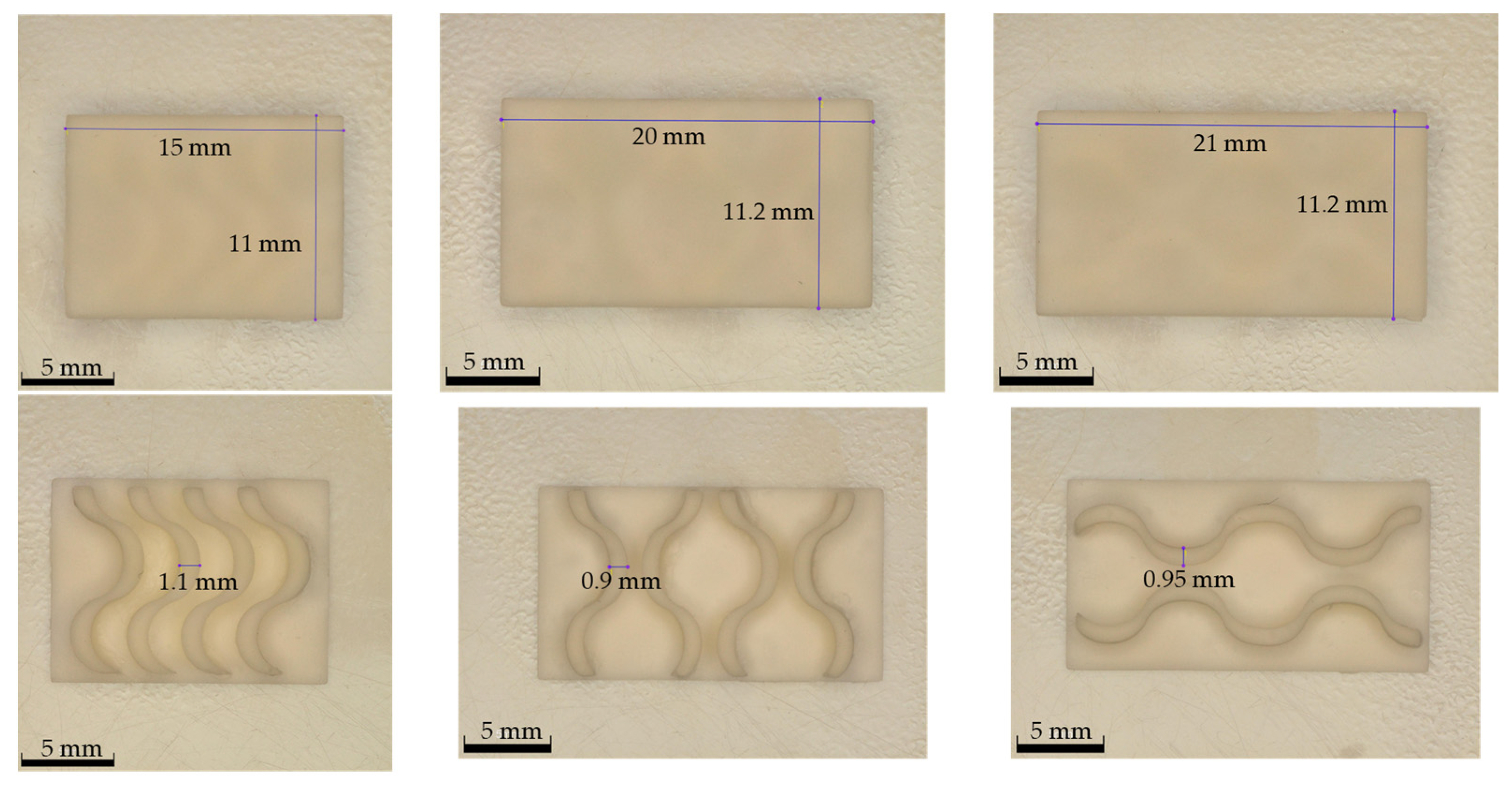
The printed and post-treated substrates are reported in Figure 11 below. As can be deduced from the measures, a shrinkage phenomenon took place during the sintering step, which is the rationale behind the selected dimensions for the 3D CAD models reported.
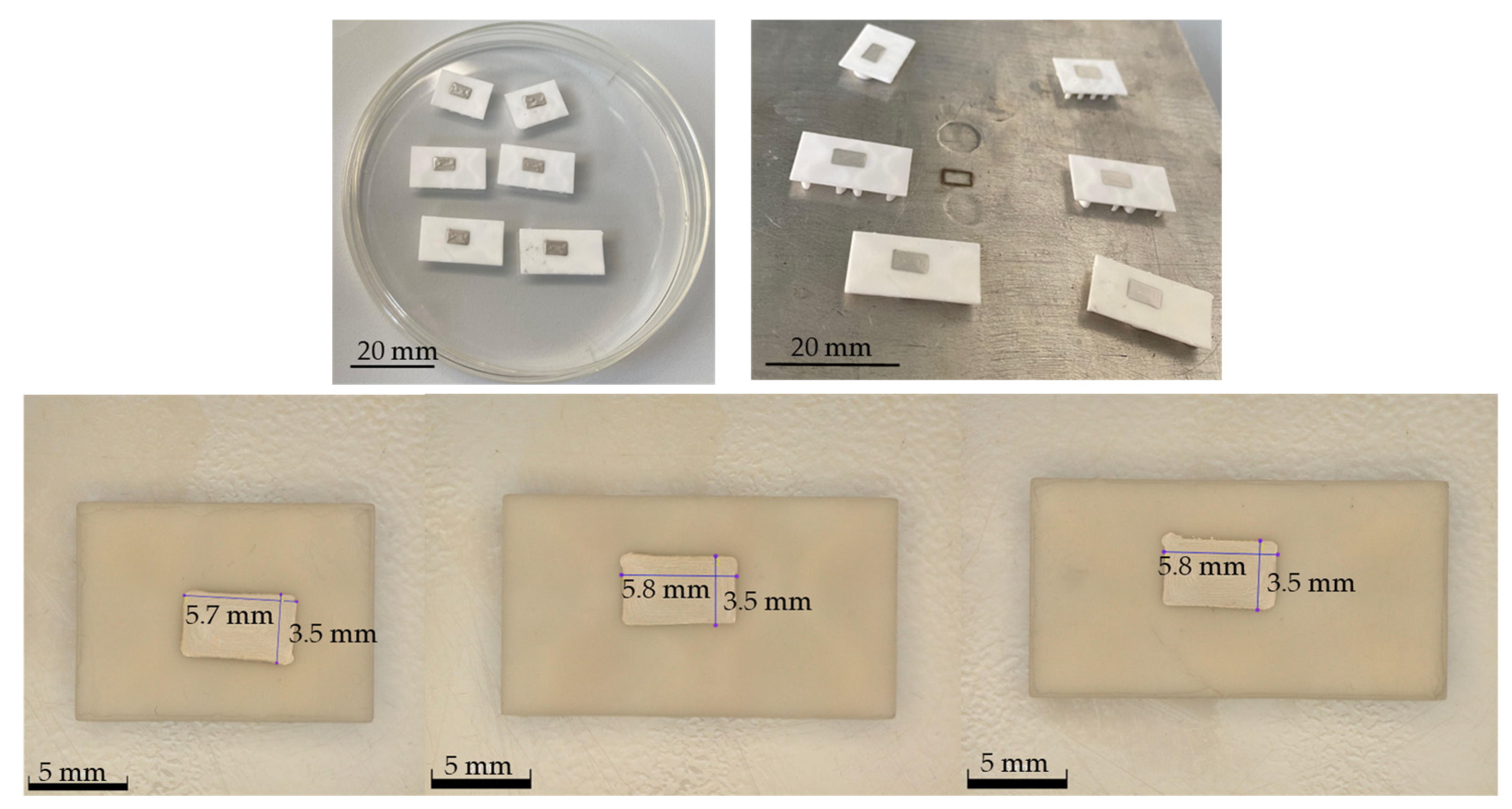
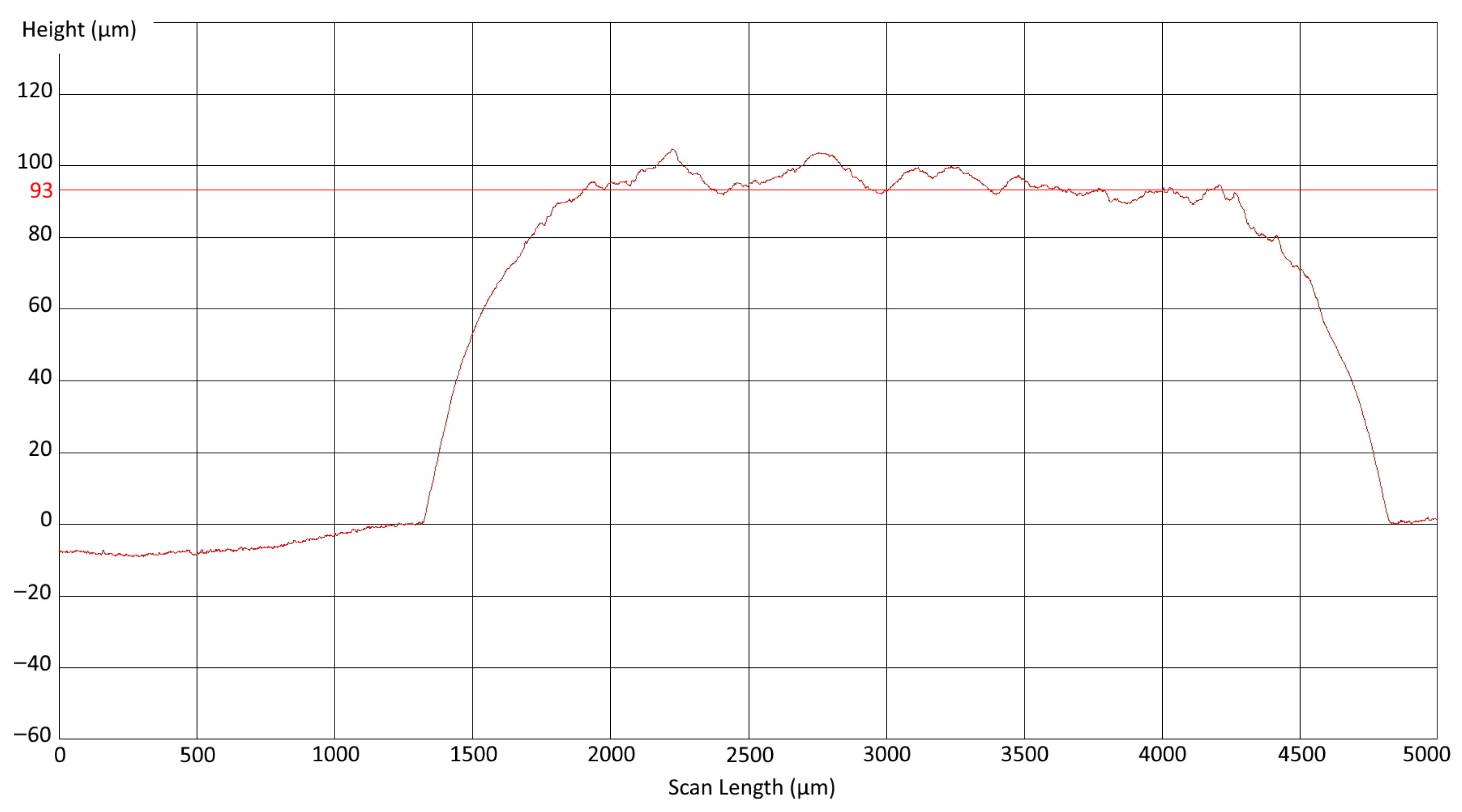
Lastly, the design of a dedicated baseplate for each printed part guaranteed a smooth plane surface, which was used for the deposition of the conductive silver paste, as in Figure 12. A profile of the deposited silver layer can be seen in Figure 13.

3.3. Die Attach

Once the reflow oven soldering process was finished, the samples were taken and analysed under a microscope. The aim of this analysis was to confirm that the paste had melted evenly and that the die was firmly attached to the substrate.
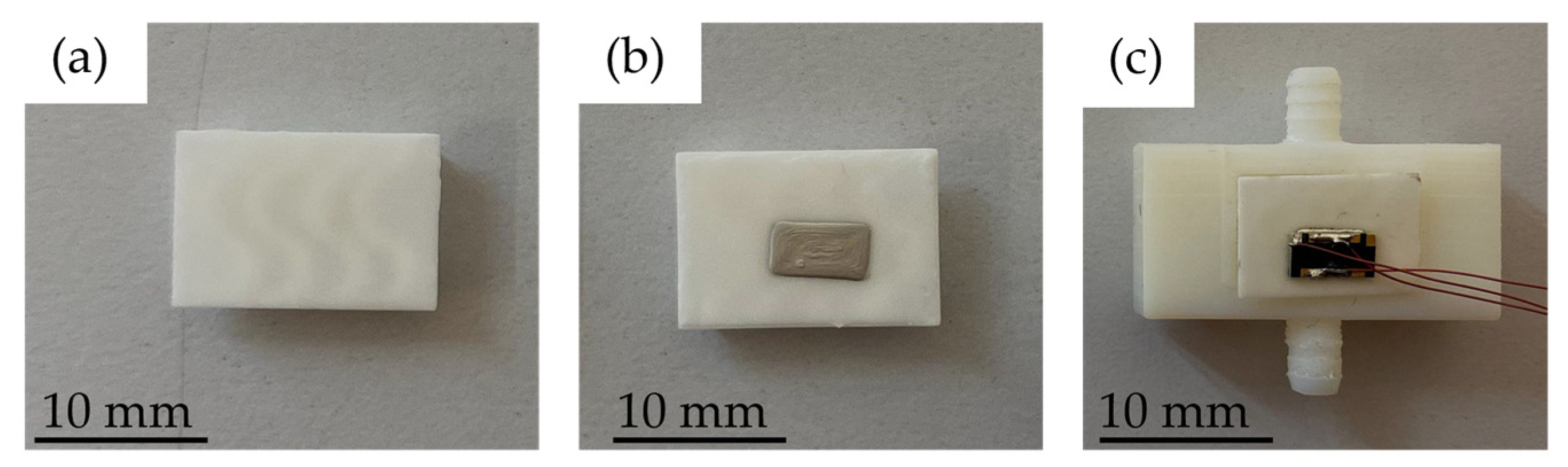
The die attach process has been successfully completed: the die remained firmly attached during testing. Lastly, the assembled devices were inserted into the designed container used for the subsequent test, as reported in Figure 14 below.

3.4. Testing

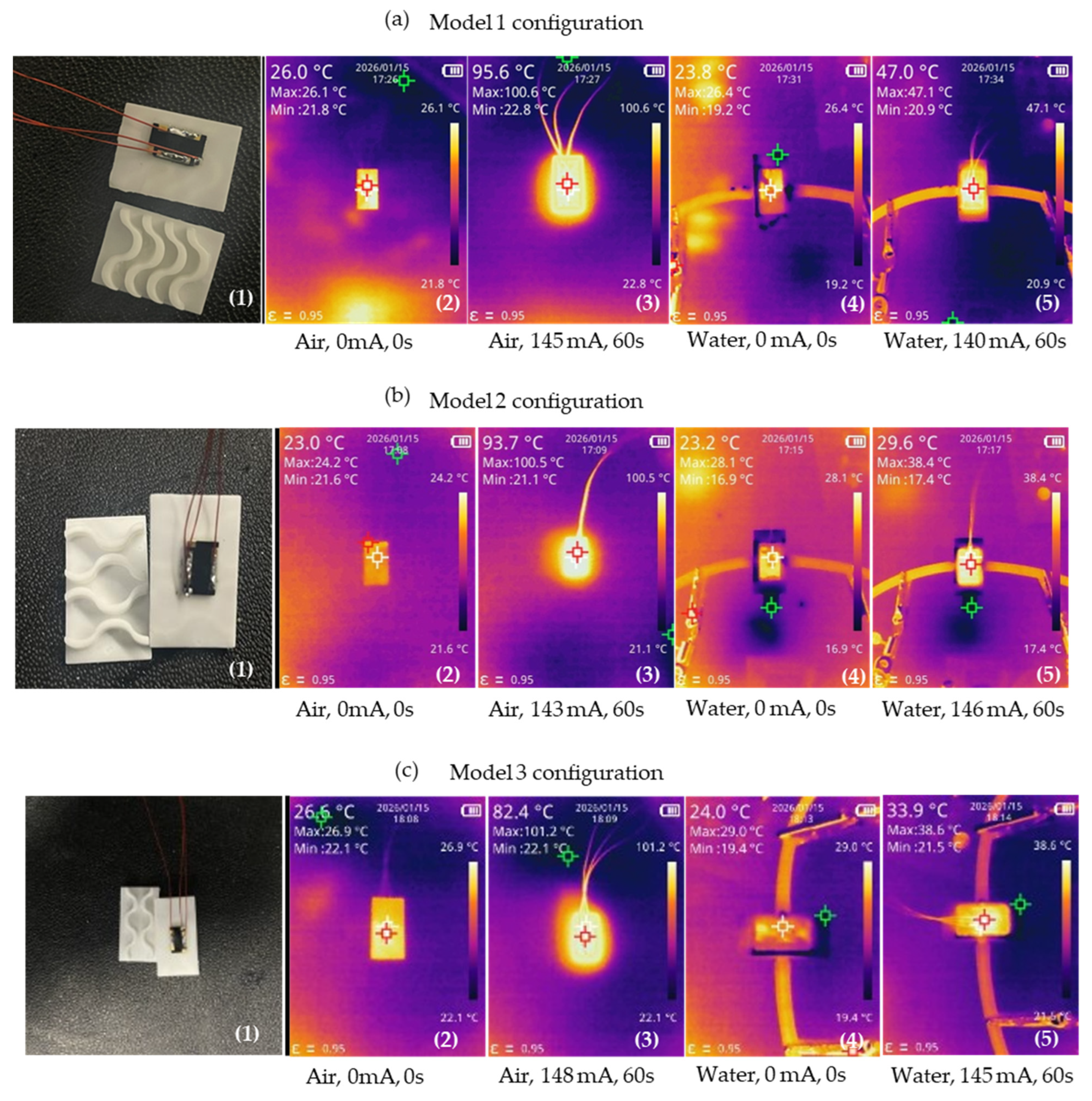
The thermal response of the three model configurations was evaluated using infrared (IR) thermography to assess their heating efficiency and heat dissipation characteristics. Figure 15a–c illustrates the steady-state thermal profiles under two distinct environmental conditions: ambient air and submerged in water. In all three configurations, the application of a constant current (approximately 140–145 mA) for 60 s resulted in a localized temperature increase concentrated at the device core. The thermal images show a distinct hot spot, with heat radiation extending slightly into the surrounding substrate. Configuration (a) exhibited a broader thermal footprint compared to (b) and (c), which showed more confined heat localization.
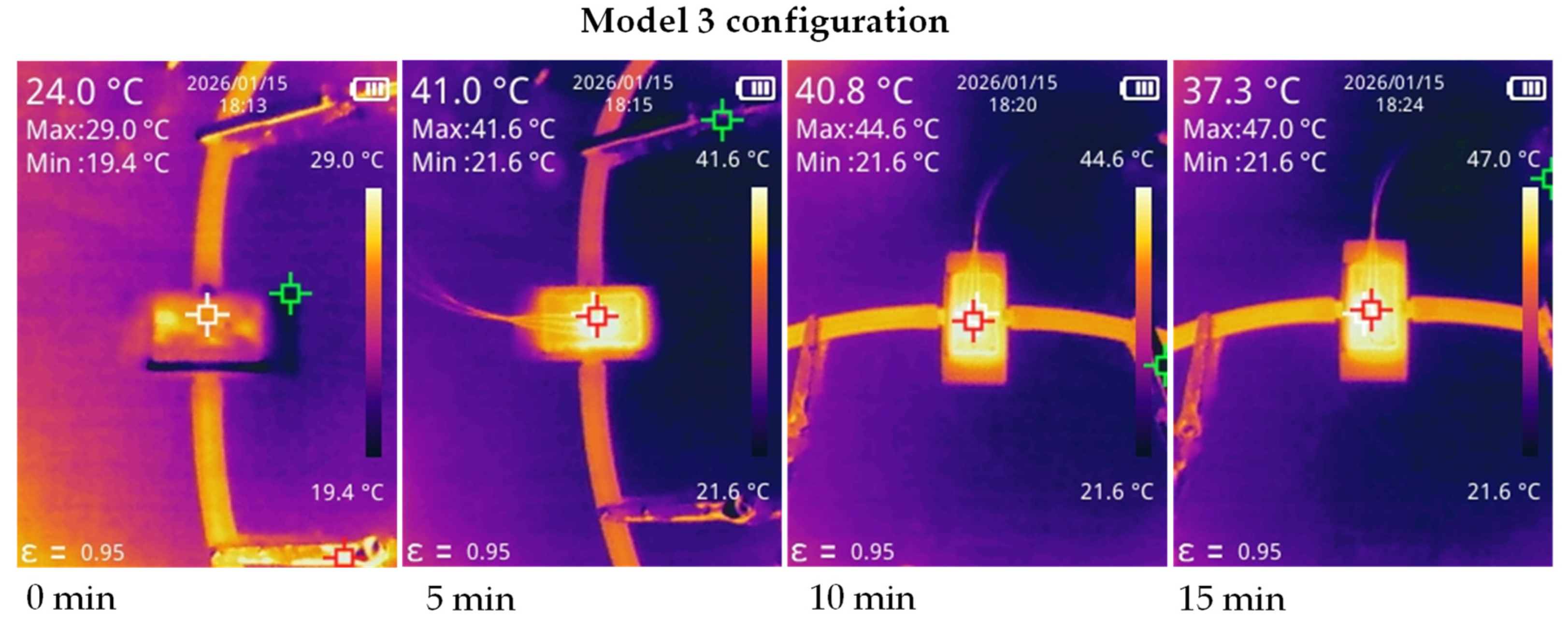
Figure 16 shows the temporal evolution of the surface temperature of the device in model 3 configuration under a constant input current of 145 mA over a 15 min ON-time with different pictures taken every 5 min. The thermal images indicate a progressive increase in peak temperature of the die with time under constant current operation, with heat primarily concentrated at the central component and limited thermal diffusion to the surrounding elements. At the end of the test (15 min), the maximum recorded temperature reached 47.0 °C.

3.5. Thermal Characterization

Thermal resistance values for the three models were evaluated and calculated for both simulated and experimental samples using the following formula:
R t h = T h o t T c o l d P
where P is the dissipated power and Thot and Tcold are the maximum temperature measured on the component and the water temperature measured at the inlet, both in the simulations and in the experiments, as can be seen in Figure 7 and Figure 15. Results can be seen in Table 3.
Convective heat transfer coefficient was also calculated for each of the simulated models, according to the formula:
h = 1 R t h A
where Rth is the thermal resistance calculated in the previous step, and A is the wetted area obtained through COMSOL as the surface of the water volume in contact with the alumina heat sink [50]. Results can be seen in Table 4.

4. Discussion

As clearly emerging from simulations, module 3 geometry is opposing the fluid flow much more than the previous versions. As it is visible in Figure 9c, this generates a slightly bigger pressure drop across the water chamber, if compared to module 1, and a slightly higher average velocity, as shown in Figure 8c. This, together with its higher heat exchange surface, seems to increase its dissipation capabilities, lowering the overall maximum temperature, as shown in Figure 7d. As far as the heat exchange surface is concerned, the three CAD models were designed to increase it. In model 1, a different amount of heat exchange free area can be quantified as 278.8 mm2 for the substrate without the additional fin structures and as 744.7 mm2 for the full version of model 1. Model 2 free available area can be quantified as 377 mm2 in the absence of the additional fin structures, and as 815.8 mm2 for the full version of model 2. Model 3, instead, showed 390 mm2 in the absence of the additional fin structures, and 787.6 mm2 in the full version of Model 3. These last two designs, compared to model 1, were inspired by a reference structure, the de Laval-like nozzle geometry. It was selected to better direct and accelerate the fluid flux below the component.
The operational conditions under which the testing was conducted simulate a scenario where the device is required to undergo continuous power-on and power-off cycles.
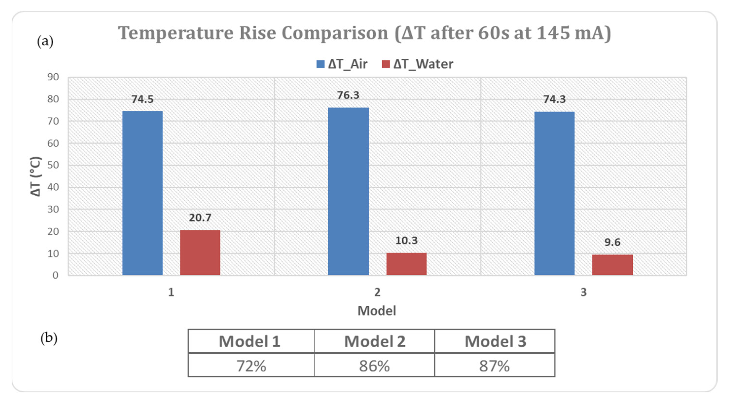
A first observation emerges from the comparison between tests performed in air and those conducted in water. For all three investigated configurations, the application of the same current input for a duration of 60 s resulted in a temperature reduction when the device was operated in water compared with the air-cooled condition. This temperature difference can be primarily attributed to the superior thermal properties of water that exhibits a thermal conductivity (~0.6 W·m−1·K−1) nearly an order of magnitude greater than that of air (~0.026 W·m−1·K−1) and to a substantially higher volumetric heat capacity. Figure 17 shows that in air, all models exhibit a pronounced and nearly uniform temperature increase, with ΔT values ranging between approximately 74 °C and 76 °C, indicating consistent thermal behaviour across the different configurations. This similarity suggests that, under air-cooled conditions, heat dissipation is primarily limited by the surrounding medium rather than by device-to-device design variations.
In contrast, operation in water results in a substantial reduction of the temperature rise for all devices. The measured ΔT values decrease to approximately 21 °C for model 1 and to about 10 °C for models 2 and 3. The observed reduction highlights the strong influence of the cooling environment on the effective thermal resistance of the system. From a thermal engineering perspective, this behaviour can be attributed to the significantly higher thermal conductivity and convective heat transfer coefficient of water compared to air, which enables more efficient removal of the heat generated by Joule dissipation. From an electronics and system design standpoint, the resulting lower temperature rise directly translates into reduced junction and case temperatures for a given input current, thereby improving operational reliability and extending component lifetime.
These characteristics lead to enhanced convective heat transfer and more efficient removal of the power dissipated at the device surface, further facilitated by the large surface area directly exposed to the liquid. Also, from an electronics perspective, the resulting reduction in effective thermal resistance translates into lower junction and case temperatures for a given input current, improving operational reliability and potentially extending component lifetime.
A second observation concerns the thermal behaviour of the system under the selected operating conditions. By utilizing a closed-loop experimental arrangement, the setup effectively isolated the heat dissipation characteristics inherent solely to the device’s architecture. Under these specific conditions, the intrinsic thermal management of the device prevents heat accumulation; instead, the temperature decreases and stabilizes at a lower steady-state equilibrium without the requirement for external cooling systems. This self-regulating thermal efficiency offers significant potential for the development of more compact, lightweight systems, as it eliminates the need for bulky dissipation hardware and facilitates more streamlined integration into the final application.
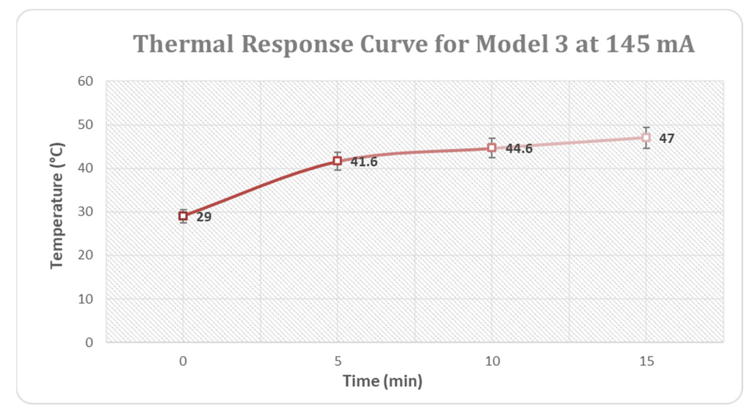
Among the tested device configurations, model 3 exhibited the most favourable thermal performance; therefore, a medium–long duration test was conducted to evaluate the temporal stability of its operating temperature under static ON test. As shown in Figure 18, the temperature initially increases from approximately 29 °C to 41.6 °C within the first 5 min, corresponding to an average heating rate of about 2.4 °C/min. This initial phase is characterized by rapid thermal transients, during which internally generated heat exceeds the heat dissipated to the surrounding environment. Beyond 5 min, marked by the dashed line in the graph, the temperature rise significantly slows down, increasing from 41.6 °C to approximately 47 °C over the subsequent 10 min. In this regime, the effective heating rate decreases to approximately 0.54 °C/min, representing a reduction of about 77% compared to the initial heating phase.
This pronounced flattening reported on the thermal response curve indicates that the system approaches a quasi–steady-state condition, in which the rate of heat generation becomes nearly balanced by the rate of heat dissipation. From a thermal physics standpoint, this behaviour suggests that the device–environment system transitions from a transient-dominated regime to a near-equilibrium state, characterized by a markedly reduced temperature gradient. Such stabilization is a strong indicator of effective passive thermal management and confirms that device 3 can sustain prolonged operation without experiencing a significant temperature runaway.

5. Conclusions

Device operating conditions characterized by repeated on/off switching are typical of high-efficiency electronic actuators, IoT sensing nodes, laser systems, and power conversion modules, which commonly operate in pulsed modes. For this reason, it is essential to consider cooling solutions that are both innovative from a thermal management perspective and capable of delivering high performance while remaining compatible with highly integrated and miniaturized system architectures.
In this context, the present research successfully demonstrates that additive manufacturing for electronics (AME) represents a rapid and flexible prototyping approach for the development and integration of advanced cooling solutions, enabling effective thermal management without compromising system compactness. Additively manufactured substrates for WBG, that include cooling strategies, were here simulated, fabricated, tested, and compared, to verify both the reliability of the digital twin and the effectiveness of the adopted solution. In this context, the three developed designs showed an efficient thermal exchange with the selected cooling medium, water, compared to the behaviour in air. In particular, models 2 and 3 demonstrated the best thermal response, achieving a temperature reduction exceeding 80% when transitioning from air to water cooling. A close agreement between experimental measurements and simulated thermal behavior was observed for all models, confirming that the digital twin accurately reproduces real operating conditions.
In this context, the present research successfully demonstrates that additive manufacturing for electronics (AME) represents a rapid and flexible prototyping approach for the development and integration of advanced cooling solutions, enabling effective thermal management without compromising system compactness. Additively manufactured substrates for WBG, that include cooling strategies, were here simulated, fabricated, tested, and compared, to verify both the reliability of the digital twin and the effectiveness of the adopted solution. In this context, the three developed designs showed an efficient thermal exchange with the selected cooling medium, water, compared to the behaviour in air. Comparing the testing results with the simulated thermal behaviour, it appears clear that the realized digital twin for all the designed models reflects their real conditions accurately. The digital twin developed is proven capable of predicting the thermal behaviour of the module. Further research will also be dedicated to matching some dynamic boundary conditions of the electrical problem. This framework allows for testing different heatsink designs and materials, further improving the sustainability by including recycled materials.
Moreover, the achieved results provide a solid foundation for future advancements, including the integration of external cooling solutions to support applications requiring prolonged continuous operation.

Author Contributions

Conceptualization and methodology, G.G., M.A. and G.M. (Giulia Mossotti); software, G.G. and D.G.; validation, M.A., D.G. and E.A.; formal analysis, D.G., E.A. and M.A.; investigation, M.M., M.A. and G.M. (Giulia Mossotti); resources, M.M. and G.M. (Gianluca Melis); data curation, G.G. and G.M. (Giulia Mossotti); writing—original draft preparation, G.G., D.G., E.A., M.A. and G.M. (Giulia Mossotti); writing—review and editing, V.B. and G.M. (Gianluca Melis); visualization, M.A. and G.M. (Giulia Mossotti); supervision, S.F. and L.S.; project administration and funding acquisition, V.B., S.F. and L.S. All authors have read and agreed to the published version of the manuscript.

Funding

The work was partially supported by the research grant “SVINBO—SILICON VALLEY 8.0 IN Piedmont FOR A GREEN AND SMART MOBILITY funded by the Italian Ministry of Economic Development DM 09.12.2014 s.m.i.—Contratto di sviluppo” (CUP: C17J23000030001-CDS0000965).

Data Availability Statement

The data presented in this study are available on request from the corresponding author due to ongoing collaborative study, and access requires approval from the project partners.

Acknowledgments

This publication was produced while attending the PhD programme in Electrical, Electronics and Communications Engineering at Politecnico di Torino, Cycle XXXIX, with the support of a scholarship financed by the Ministerial Decree no. 118 of 2 March 2023, based on the NRRP—funded by the European Union—Next Generation EU—Mission 4 “Education and Research”, Component 1 “Enhancement of the offer of educational services: from nurseries to universities”—Investment 3.4 “Advanced teaching and university skills”.

Conflicts of Interest

Author Massimiliano Messere was employed by the company Microla srl. The remaining authors declare that this research was conducted in the absence of any commercial or financial relationships that could be construed as a potential conflict of interest.

References

  1. World Energy Outlook 2025—Analysis—IEA. Available online: https://www.iea.org/reports/world-energy-outlook-2025 (accessed on 23 January 2026).
  2. Abart, C.; Berberich, K.; Hegazy, O.; Abdel-Monem, M.; Vanegas, O.; Lis, A. Wide Bandgap Semiconductors Enabling Highly Efficient Electrified Vehicles. Transp. Res. Procedia 2023, 72, 17–23. [Google Scholar] [CrossRef]
  3. Rymarski, Z.; Ptak, P. Special Issue: New Technologies for Power Electronic Converters and Inverters. Appl. Sci. 2025, 15, 5753. [Google Scholar] [CrossRef]
  4. He, J.; Cheng, W.C.; Wang, Q.; Cheng, K.; Yu, H.; Chai, Y. Recent Advances in GaN-Based Power HEMT Devices. Adv. Electron. Mater. 2021, 7, 2001045. [Google Scholar] [CrossRef]
  5. Wang, M.; Gao, P.; Shi, F.; Hu, W.; Wang, X.; Yan, H.; Mei, Y. Advanced Packaging Technology of GaN HEMT Module for High-Power and High-Frequency Applications: A Review. IEEE Trans. Compon. Packag. Manuf. Technol. 2024, 14, 1537–1550. [Google Scholar] [CrossRef]
  6. Sun, R.; Lai, J.; Chen, W.; Zhang, B. GaN Power Integration for High Frequency and High Efficiency Power Applications: A Review. IEEE Access 2020, 8, 15529–15542. [Google Scholar] [CrossRef]
  7. Derkacz, P.B.; Schanen, J.L.; Jeannin, P.O.; Musznicki, P.; Chrzan, P.J.; Petit, M. 3D PCB Package for GaN Inverter Leg with Low EMC Feature. In Proceedings of the 2020 22nd European Conference on Power Electronics and Applications, EPE 2020 ECCE Europe, Lyon, France, 7–11 September 2020. [Google Scholar] [CrossRef]
  8. Lu, J.L.; Hou, R.; Chen, D. Opportunities and Design Considerations of GaN HEMTs in ZVS Applications. In Proceedings of the IEEE Applied Power Electronics Conference and Exposition—APEC, San Antonio, TX, USA, 4–8 March 2018; pp. 880–885. [Google Scholar] [CrossRef]
  9. Spano, C.; Galfre’, G.; Mattiuzzo, E.; D’Ancona, L.; Bertana, V.; Scaltrito, L.; Ferrero, S. Evaluation of the Thermal Fatigue and Failure Mechanisms on Power Modules with Different Types of Substrates (DBC/IMS). ETG-Fachber. 2024, 173, 103–109. [Google Scholar]
  10. Cheng, T.H.; Nishiguchi, K.; Fukawa, Y.; Hopkins, D.C. Thermal and Reliability Performance Comparison of DBC-Based and Organic-Based Double-Sided Cooled Power Modules. In Proceedings of the 54th International Symposium on Microelectronics, San Diego, CA, USA, 11–14 October 2021; Volume 2021, pp. 382–389. [Google Scholar] [CrossRef]
  11. Górecki, K.; Posobkiewicz, K. Cooling Systems of Power Semiconductor Devices—A Review. Energies 2022, 15, 4566. [Google Scholar] [CrossRef]
  12. Kandlikar, S.G.; Upadhye, H.R. Extending the Heat Flux Limit with Enhanced Microchannels in Direct Single-Phase Cooling of Computer Chips. In Proceedings of the Annual IEEE Semiconductor Thermal Measurement and Management Symposium, San Jose, CA, USA, 15–17 March 2005; pp. 8–15. [Google Scholar] [CrossRef]
  13. Tang, W.; Huang, X.; Chen, Z.; Sheng, K.; Wu, Z. Uniform and Efficient Embedded Microfluidic Cooling for High-Power-Density Power Modules. IEEE Trans. Power Electron. 2025, 40, 14524–14535. [Google Scholar] [CrossRef]
  14. Wang, P.; Mccluskey, P.; Bar-Cohen, A. Two-Phase Liquid Cooling for Thermal Management of Igbt Power Electronic Module. J. Electron. Packag. 2013, 135, 021001. [Google Scholar] [CrossRef]
  15. Li, J.; Zhang, H. Thermal Characteristics of Power Battery Module with Composite Phase Change Material and External Liquid Cooling. Int. J. Heat Mass Transf. 2020, 156, 119820. [Google Scholar] [CrossRef]
  16. Hoang, C.H.; Rangarajan, S.; Manaserh, Y.; Tradat, M.; Mohsenian, G.; Choobineh, L.; Ortega, A.; Schiffres, S.; Sammakia, B. A Review of Recent Developments in Pumped Two-Phase Cooling Technologies for Electronic Devices. IEEE Trans. Compon. Packag. Manuf. Technol. 2021, 11, 1565–1582. [Google Scholar] [CrossRef]
  17. Qu, W.; Mudawar, I. Measurement and Prediction of Pressure Drop in Two-Phase Micro-Channel Heat Sinks. Int. J. Heat Mass Transf. 2003, 46, 2737–2753. [Google Scholar] [CrossRef]
  18. Rong, X.; Wu, R.; Mawby, P. A Newly Designed Double-Sided Cooling Wire-Bondless Power Module with Silicon Carbide MOSFETs and Ultra-Low Stray Inductance. Electronics 2025, 14, 1520. [Google Scholar] [CrossRef]
  19. Stevanovic, L.D.; Beaupre, R.A.; Gowda, A.V.; Pautsch, A.G.; Solovitz, S.A. Integral Micro-Channel Liquid Cooling for Power Electronics. In Proceedings of the IEEE Applied Power Electronics Conference and Exposition—APEC, Palm Springs, CA, USA, 21–25 February 2010; pp. 1591–1597. [Google Scholar] [CrossRef]
  20. Birbarah, P.; Gebrael, T.; Foulkes, T.; Stillwell, A.; Moore, A.; Pilawa-Podgurski, R.; Miljkovic, N. Water Immersion Cooling of High Power Density Electronics. Int. J. Heat Mass Transf. 2020, 147, 118918. [Google Scholar] [CrossRef]
  21. Bahiraei, M.; Heshmatian, S. Electronics Cooling with Nanofluids: A Critical Review. Energy Convers. Manag. 2018, 172, 438–456. [Google Scholar] [CrossRef]
  22. Kang, S.S. Advanced Cooling for Power Electronics. In Proceedings of the 2012 7th International Conference on Integrated Power Electronics Systems (CIPS), Nuremberg, Germany, 6–8 March 2012. [Google Scholar]
  23. Hesselgreaves, J.E. Compact Heat Exchangers: Selection, Design, and Operation; Pergamon: Berlin, Germany, 2001; ISBN 0080428398. [Google Scholar]
  24. Li, Y.; Roux, S.; Castelain, C.; Fan, Y.; Luo, L. Design and Optimization of Heat Sinks for the Liquid Cooling of Electronics with Multiple Heat Sources: A Literature Review. Energies 2023, 16, 7468. [Google Scholar] [CrossRef]
  25. Ahmed, H.E.; Salman, B.H.; Kherbeet, A.S.; Ahmed, M.I. Optimization of Thermal Design of Heat Sinks: A Review. Int. J. Heat Mass Transf. 2018, 118, 129–153. [Google Scholar] [CrossRef]
  26. Cui, P.; Liu, Z. Enhanced Flow Boiling of HFE-7100 in Picosecond Laser Fabricated Copper Microchannel Heat Sink. Int. J. Heat Mass Transf. 2021, 175, 121387. [Google Scholar] [CrossRef]
  27. Li, Y.F.; Xia, G.D.; Ma, D.D.; Jia, Y.T.; Wang, J. Characteristics of Laminar Flow and Heat Transfer in Microchannel Heat Sink with Triangular Cavities and Rectangular Ribs. Int. J. Heat Mass Transf. 2016, 98, 17–28. [Google Scholar] [CrossRef]
  28. Singh, S.; Malik, A.; Mali, H.S. A Critical Review on Single-Phase Thermo-Hydraulic Enhancement in Geometrically Modified Microchannel Devices. Appl. Therm. Eng. 2023, 235, 121729. [Google Scholar] [CrossRef]
  29. Uygun, Y. The Fourth Industrial Revolution—Industry 4.0. In Industry 4.0: Principles, Effects and Challenges; Uygun, Y., Ed.; Nova Science: Hauppauge, NY, USA, 2021; pp. 3–15. [Google Scholar]
  30. Khorasani, M.; Loy, J.; Ghasemi, A.H.; Sharabian, E.; Leary, M.; Mirafzal, H.; Cochrane, P.; Rolfe, B.; Gibson, I. A Review of Industry 4.0 and Additive Manufacturing Synergy. Rapid Prototyp. J. 2022, 28, 1462–1475. [Google Scholar] [CrossRef]
  31. Vasudev, H.; In, H.; Prashar, G.; Bhuddhi, D.; Vasudev, H.; Bhuddhi, D. Additive Manufacturing: Expanding 3D Printing Horizon in Industry 4.0. Int. J. Interact. Des. Manuf. (IJIDeM) 2022, 17, 2221–2235. [Google Scholar] [CrossRef]
  32. Tan, H.W.; Choong, Y.Y.C.; Kuo, C.N.; Low, H.Y.; Chua, C.K. 3D Printed Electronics: Processes, Materials and Future Trends. Prog. Mater. Sci. 2022, 127, 100945. [Google Scholar] [CrossRef]
  33. Godec, D.; Pilipović, A.; Breški, T. General Process Workflow in Additive Manufacturing. In A Guide to Additive Manufacturing. Springer Tracts in Additive Manufacturing; Godec, D., Gonzalez-Gutierrez, J., Nordin, A., Pei, E., Ureña Alcázar, J., Eds.; Springer: Cham, Switerland, 2024; pp. 45–57. [Google Scholar] [CrossRef]
  34. Tamir, T.S.; Xiong, G.; Shen, Z.; Leng, J.; Fang, Q.; Yang, Y.; Jiang, J.; Lodhi, E.; Wang, F.Y. 3D Printing in Materials Manufacturing Industry: A Realm of Industry 4.0. Heliyon 2023, 9, e19689. [Google Scholar] [CrossRef] [PubMed]
  35. Delmonte, N.; Spaggiari, D.; Sciancalepore, C.; Menozzi, R.; Cova, P. FEM-Based Development of Novel 3D-Printable Plastic Direct Coolers for Power Semiconductor Modules. Microelectron. Reliab. 2025, 167, 115671. [Google Scholar] [CrossRef]
  36. Howard, D. The Digital Twin: Virtual Validation In Electronics Development And Design. In Proceedings of the 2019 Pan Pacific Microelectronics Symposium, Pan Pacific 2019, Kauai, HI, USA, 11–14 February 2019. [Google Scholar] [CrossRef]
  37. Icoz, T.; Verma, N.; Jaluria, Y. Design of Air and Liquid Cooling Systems for Electronic Components Using Concurrent Simulation and Experiment. J. Electron. Packag. 2006, 128, 466–478. [Google Scholar] [CrossRef]
  38. Mamatha, S.; Biswas, P.; Johnson, R. Digital Light Processing of Ceramics: An Overview on Process, Materials and Challenges. Prog. Addit. Manuf. 2022, 8, 1083–1102. [Google Scholar] [CrossRef]
  39. Swetha, S.; Sahiti, T.J.; Priya, G.S.; Harshitha, K.; Anil, A. Review on Digital Light Processing (DLP) and Effect of Printing Parameters on Quality of Print. Interactions 2024, 245, 178. [Google Scholar] [CrossRef]
  40. Aronne, M.; Polano, M.; Bertana, V.; Ferrero, S.; Frascella, F.; Scaltrito, L.; Marasso, S.L. Application of 3D and 4D Printing in Electronics. J. Manuf. Mater. Process. 2024, 8, 164. [Google Scholar] [CrossRef]
  41. Thakur, V.; Singh, R.; Kumar, R.; Gehlot, A. 4D Printing of Thermoresponsive Materials: A State-of-the-Art Review and Prospective Applications. Int. J. Interact. Des. Manuf. (IJIDeM) 2022, 17, 2075–2094. [Google Scholar] [CrossRef]
  42. Daniela, L.; Briceño, S.; In Biomedical, M.S.; Osma, J.F. Exploration of Electrode Manufacturing Methods for the Fabrication of Biosensors Integrated with Microfluidics, for PFAs Detection. Master’s Thesis, Biomedical Engineering Department, Universidad de Los Andes, Bogotá, Colombia, 2025. Available online: https://share.google/B2bnBZPtzHDB261KI (accessed on 24 February 2026).
  43. Infineon GS61008T Top-Side Cooled 100 V E-Mode GaN Transistor Datasheet. Available online: https://www.infineon.com/assets/row/public/documents/24/49/infineon-gs61008t-datasheet-en.pdf?fileId=8ac78c8c8d2fe47b018e5160eb52522a (accessed on 24 February 2026).
  44. COMSOL Documentation. Available online: https://doc.comsol.com/6.4/docserver/#!/com.comsol.help.comsol/comsol_ref_materials.25.01.html (accessed on 23 January 2026).
  45. Ceramics—Admatec. Available online: https://admateceurope.com/ceramics/ (accessed on 20 February 2026).
  46. NSM Archive—Gallium Nitride (GaN). Available online: https://www.ioffe.ru/SVA/NSM/Semicond/GaN/ (accessed on 23 January 2026).
  47. Lauga, E.; Brenner, M.; Stone, H. Microfluidics: The No-Slip Boundary Condition; Springer Handbooks; Springer: Berlin/Heidelberg, Germany, 2005; pp. 1219–1240. [Google Scholar] [CrossRef]
  48. Cicolini, M.; Solgi, A.; Vigna, L.; Ballesio, A.; Marasso, S.; Cocuzza, M.; Kleemann, H.; Frascella, F.; Napione, L. A Printable OECT for Simple Integration in Nitrocellulose-Based Assays. ACS Sens. 2025, 10, 7630–7638. [Google Scholar] [CrossRef] [PubMed]
  49. Rao, C.H.; Avinash, K.; Varaprasad, B.K.S.V.L.; Goel, S. A Review on Printed Electronics with Digital 3D Printing: Fabrication Techniques, Materials, Challenges and Future Opportunities. J. Electron. Mater. 2022, 51, 2747–2765. [Google Scholar] [CrossRef]
  50. Hesselgreaves, J.E.; Law, R.; Reay, D.A. Compact Heat Exchangers Selection, Design and Operation; Elsevier Ltd.: Amsterdam, The Netherlands, 2021; ISBN 978-0-08-042839-0. [Google Scholar]
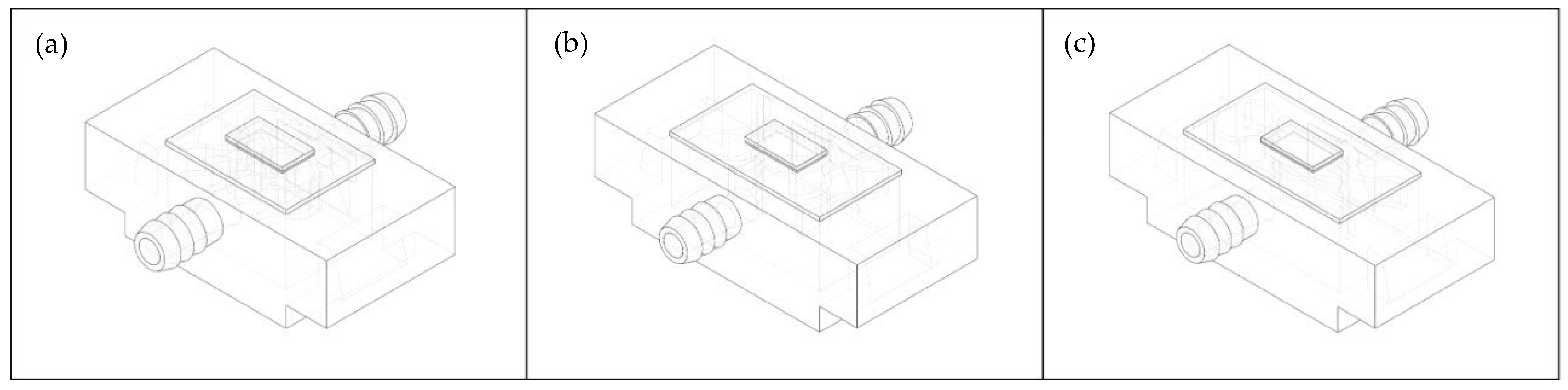
Figure 1. 3D CAD models used in the simulations. (a) model 1, cavity volume: 14.7 mm × 10.7 mm × 8.2 mm; (b) model 2, cavity volume: 19.7 mm × 10.7 mm × 8.2 mm; (c) model 3, cavity volume: 20.78 mm × 10.7 mm × 8.2 mm.
Electronics 15 01002 g001
Figure 2. CAD design of the three simulated, tested, and fabricated models, reporting (a) measurements, in mm, of the areas of the three models, and (b) measurements, in mm, of the thicknesses of the three models. Both (a,b) show the designed baseplates, used for improving the parts’ adhesion and promoting the subsequent detachment at the end of the print job.
Electronics 15 01002 g002
Figure 3. Image from the printer slicing setting, reporting the layer division used.
Electronics 15 01002 g003
Figure 4. Debinding and sintering profile used for the selected material. The red line identifies the moment where the air flux is shut down during the process. Graph realized using Matlab 2024a.
Electronics 15 01002 g004
Figure 5. Soldering profile used, based on the soldering paste and reflow oven. Graph realized using Matlab 2024a.
Electronics 15 01002 g005
Figure 6. Testing setup, showing the conditioning circuit and the multimeter used during the measurements.
Electronics 15 01002 g006
Figure 7. Temperature map of the three models after 60 s of simulation. (a) model 1 with a simulated air box surrounding it; (b) model 1 without air surrounding it; (c) model 2; (d) model 3.
Electronics 15 01002 g007
Figure 8. Water velocity field of the three models after 60 s of simulation. Water flows from right to left. (a) model 1; (b) model 2; (c) model 3.
Electronics 15 01002 g008
Figure 9. Pressure map of the three models after 60 s of simulation, measured on the walls of the fluid domain. Water flows from right to left. (a) model 1; (b) model 2; (c) model 3.
Electronics 15 01002 g009
Figure 10. Simulated model 1 without water flow as seen from above.
Electronics 15 01002 g010
Figure 11. As sintered white bodies, with related measurements, of each fabricated model.
Electronics 15 01002 g011
Figure 12. Sintered models showing the deposited silver ink, with related measures.
Electronics 15 01002 g012
Figure 13. Profile of the deposited silver layer, measured along the short dimension.
Electronics 15 01002 g013
Figure 14. Representation of the three fabrication steps: (a) printing and sintering of the designed component, (b) silver and soldering pastes deposition for the subsequent die attaching process, (c) assembled device, with the GaN component on top, ready for testing.
Electronics 15 01002 g014
Figure 15. Thermal camera recorded images of the thermal behaviour of the three models in different conditions: (a) model 1 component (1) behaviour was observed at (2) 0 mA in air, then the current was turned on (3), giving the component 145 mA for 60 s. The same configuration was studied in different conditions, starting with (4) 0 mA to (5) 140 mA for 60 s, using water as the cooling liquid. (b) Model 2 component (1) behaviour was observed at (2) 0 mA in air, then the current was turned on (3), giving the component 143 mA for 60 s. The same configuration was studied in different conditions, starting with (4) 0 mA to (5) 146 mA for 60 s, using water as the cooling liquid. (c) model 3 component (1) behaviour was observed at (2) 0 mA in air, then the current was turned on (3), giving the component 148 mA for 60 s. The same configuration was studied in different conditions, starting with (4) 0 mA to (5) 145 mA for 60 s, using water as the cooling liquid. The three temperature indicators, presenting different colours, identify the points where the minimum (green) and the maximum (red) temperatures are reached, together with the indication (white) of the point under test.
Electronics 15 01002 g015
Figure 16. Measured temperature profile of model 3 as a function of time (0–15 min) under a constant input current of 145 mA. The three temperature indicators, presenting different colours, identify the points where the minimum (green) and the maximum (red) temperatures are reached, together with the indication (white) of the point under test.
Electronics 15 01002 g016
Figure 17. For the three device models tested in air and in water, (a) the graph compares the temperature rise (ΔT) measured after 60 s at an input current of 145 mA; (b) the percentage of temperature reduction.
Electronics 15 01002 g017
Figure 18. Thermal Response Curve: the long-term thermal behaviour of the temperature monitored over a time window ranging from 0 to 15 min at a constant input current of 145 mA for model 3.
Electronics 15 01002 g018
Table 1. Summary of properties of the materials used in the FEM simulation.
MaterialDynamic Viscosity [Pa·s]Density [kg/m3]Heat Capacity [J/kg·K]Thermal Conductivity [W/m·K]Notes
Acrylic Plastic-119014700.18See COMSOL documentation [44]
Air at 16 °C1.79 × 10−51.2210050.026
Gold-19,300129317
Silicon-2329700130
Silver-10,500235429
Solder Paste-900015050
Water at 16 °C1.1 × 10−3100041910.59
Alumina-390090030[44,45]
GaN-6150490130[46]
Table 2. Summary of the used parameters for the models’ printing processes.
LayersParameterValue
0 (base)Layer thickness (µm)50
Led power (‰)600
Exposure time (s)25
1–32 (baseplate)Layer thickness (µm)30
Led power (‰)600
Exposure time (s)5
33 (over curing layer)Layer thickness (µm)30
Led power (‰)600
Exposure time (s)50
34 (under curing layer)Layer thickness (µm)60
Led power (‰)600
Exposure time (s)5
35–149 (parts)Layer thickness (µm)30
Led power (‰)600
Exposure time (s)5
Table 3. Thermal resistance values for each model, from both the simulation and the experimental sections.
ModelThot [°C]Tcold [°C]P [W]Rth [K/W]
Simulation
138.1161.415.79
237.5161.415.36
336.8161.414.83
Experimental
147.120.91.418.71
238.417.41.415.00
338.621.51.412.21
Table 4. Convective heat transfer values for each model used in the simulations.
ModelRth [K/W]A [m2]h [W/m2·K]
115.790.0004839130.88
215.360.0005404120.47
314.830.0005215129.30
Disclaimer/Publisher’s Note: The statements, opinions and data contained in all publications are solely those of the individual author(s) and contributor(s) and not of MDPI and/or the editor(s). MDPI and/or the editor(s) disclaim responsibility for any injury to people or property resulting from any ideas, methods, instructions or products referred to in the content.