Article

Suppression of Cross-Polarized Radiation of Rectangular Microstrip Antenna on Slot-Type Defected Ground Using Periodic Circular Structure

State Key Laboratory of Millimeter Waves, Southeast University, Nanjing 210096, China
*
Author to whom correspondence should be addressed.
Electronics 2026, 15(3), 677; https://doi.org/10.3390/electronics15030677
Submission received: 18 January 2026 / Revised: 31 January 2026 / Accepted: 2 February 2026 / Published: 4 February 2026

Abstract

A novel resonant-type defected ground structure (DGS) featuring a modified internal structure is proposed to enhance the suppression of cross-polarized (XP) radiation of rectangular microstrip antennas (RMAs) on slot-type DGS. Specifically, integrating periodic circular metal structure (PCS) into the slot-type DGS, which has been demonstrated to reduce RMA XP levels and minimize the space occupied by defects. As a resonant-type DGS, the embedding of the PCS enables the excitation of the entire DGS by the fringe field of the patch. The coupling between the fringe field and the PCS-type DGS results in a significant alteration of the field distribution of the high-order mode TM02, thereby effectively suppressing the XP radiation generated by TM02 mode. This structural concept originates from the unique control capabilities of periodic structures over electromagnetic field propagation, with the objective of optimizing the symmetry of the substrate field distribution inside the defect region. Compared to slot-type DGS, the periodic structure enables more electromagnetic fields to couple into the slot from the non-radiating side and disperse among each metal element, generating resonance in the TM02 mode field. Experiments demonstrate the H-plane co-cross polarization isolation exceeds 25 dB across an azimuth range exceeding 200°, with peak XP suppression reaching 20 dB. This performance is at the forefront of resonant-type DGSs.

1. Introduction

Rectangular microstrip antenna (RMA) has been widely applied in satellite communications, radar systems, wireless networks, and other fields. However, the inherent cross-polarized (XP) radiation issue severely limits polarization purity, particularly in H-plane [1]. The primary sources of XP can be categorized as follows: firstly, the excitation of high-order modes; secondly, field-distribution asymmetry caused by feed perturbation [2,3]. Low cross-polarization RMAs play a critical role in numerous modern wireless systems demanding stringent polarization purity, owing to their ability to enhance system capacity and accuracy. Major application scenarios include improving spectrum reuse efficiency in satellite communications, ensuring high-resolution radar/remote sensing target identification accuracy, reducing inter-user interference in 5G/6G Massive MIMO systems, and applications in radio astronomy.
Defected ground structure (DGS) has been identified as a major technological solution to such issues, with numerous generations of design schemes having been developed since their initial proposal in 2005 [4]. DGS achieves the suppression effect by etching a specifically shaped defect in the ground plane that disturbs the field or current associated with XP. Previous studies of DGS focused on structural symmetry or resonance characteristics. Kumar et al. proposed linear DGS [5] and asymmetric DGS [6,7] to effectively attenuate the effect of high-order modes on the feed-side electric field. Pasha et al. proposed a non-proximal DGS [8,9], which reconfigured the field distribution by directly interfering with the ground current distribution and accomplished XP suppression in the full plane. Recently, Qian et al. successfully blocked the field propagation path of the TM02 mode by placing the asymmetric DGS below the patch, thus avoiding the increase in back radiation and providing a decoupled array structure [10]. Rafidul first proposed an innovative approach combining multi-parameter DGS with machine learning-assisted PSADEA optimization algorithms. Resonant rectangular loop defect and corner orthogonal slits were employed to achieve improvements in XP across the entire azimuth plane [11]. As indicated above, the current optimization of DGS focuses on three aspects: defect size, defect external shape, and defect location. Beyond suppressing XP radiation, DGS has also made significant contributions in the fields of multibanding and widebanding. Rahman et al. proposed a broadband array antenna for Sub-6 GHz applications featuring a novel matching circuit and DGS, achieving an impedance bandwidth of 70% (3.05–6.32 GHz) [12]. Wang et al. proposed an antenna structure that achieves tri-band operation through two simple monopoles and an arc-shaped defect, covering the 2.4/5.2/5.8 GHz WLAN and 3.5/5.5 GHz WiMAX bands [13].
Slot-type DGS proposed in 2015 [14], as a form of external shape optimization, demonstrates substantial advantages in bandwidth expansion. Sarkar et al. achieved 56.7% impedance bandwidth by integrating the slot-type DGS with a single shorting post [15]. However, this DGS is limited in terms of design flexibility. It has been demonstrated that the RMA XP level cannot be reduced any further by simply changing the slot length in a specific frequency band. Reference [14] has shown that the wide angular range of H-plane XP radiation (below −25 dB) can reach 150° at 8.2 GHz, whereas it is merely 100° at 9.8 GHz. Additionally, an excessively large slot area may give rise to undesirable backside radiation. Nevertheless, this observation also implies that larger defect areas offer opportunities for modifying their internal structure.
In this paper, we explore the optimization of the internal structure of the DGS for the first time and overcome the limitations of the RMA with slot-type DGS polarization purity by adding periodic circular structure (PCS) inside the defects, as shown in Figure 1. The slot-type DGS is unable to fully excite the entire defect due to its large width, whereas the PCS-type DGS exhibits strong coupling with the patch corner field. This coupling consequently instigates substantial alterations in the TM02 mode field distribution, thereby more efficiently suppressing the XP radiation generated by TM02. Representative designs of C-band and X-band RMAs are provided. Based on the mode field distribution and far-field simulation, the reasons for the limitations of slot-type DGS and the superiority of PCS-type DGS in XP suppression are analyzed. Next, the investigation is carried out to excite the TM02 mode in the patch, yielding a peak reduction of 20 dB. Experiments have demonstrated that the X-band RMA based on the PCS-type DGS attains H-plane co-cross polarization isolation of over 25 dB across an azimuth range exceeding 200° and peak XP suppression up to 20 dB.

2. Design Methodology and Configuration

DGS has evolved from a “passive perturbation” to an “active synergy” paradigm in RMA XP suppression. This transformation encompasses transitions in design from a symmetrical to an asymmetrical configuration and from a proximal to a non-proximal defect. Parallel to this, advancements in performance demonstrate shifts from single H-plane suppression to entire-plane high isolation, from narrowband to broadband, and from element to array [10,16]. The core breakthrough lies in the precise matching between DGS and field distribution. PCS can modulate the intensity, spatial distribution, propagation direction, and polarization state of electric fields by virtue of the interaction between its periodic refractive index profile and electromagnetic waves [17,18,19]. Therefore, the negative effect of the high-order mode TM02 on the substrate electric field will be weakened further by incorporating a PCS inside the slot.
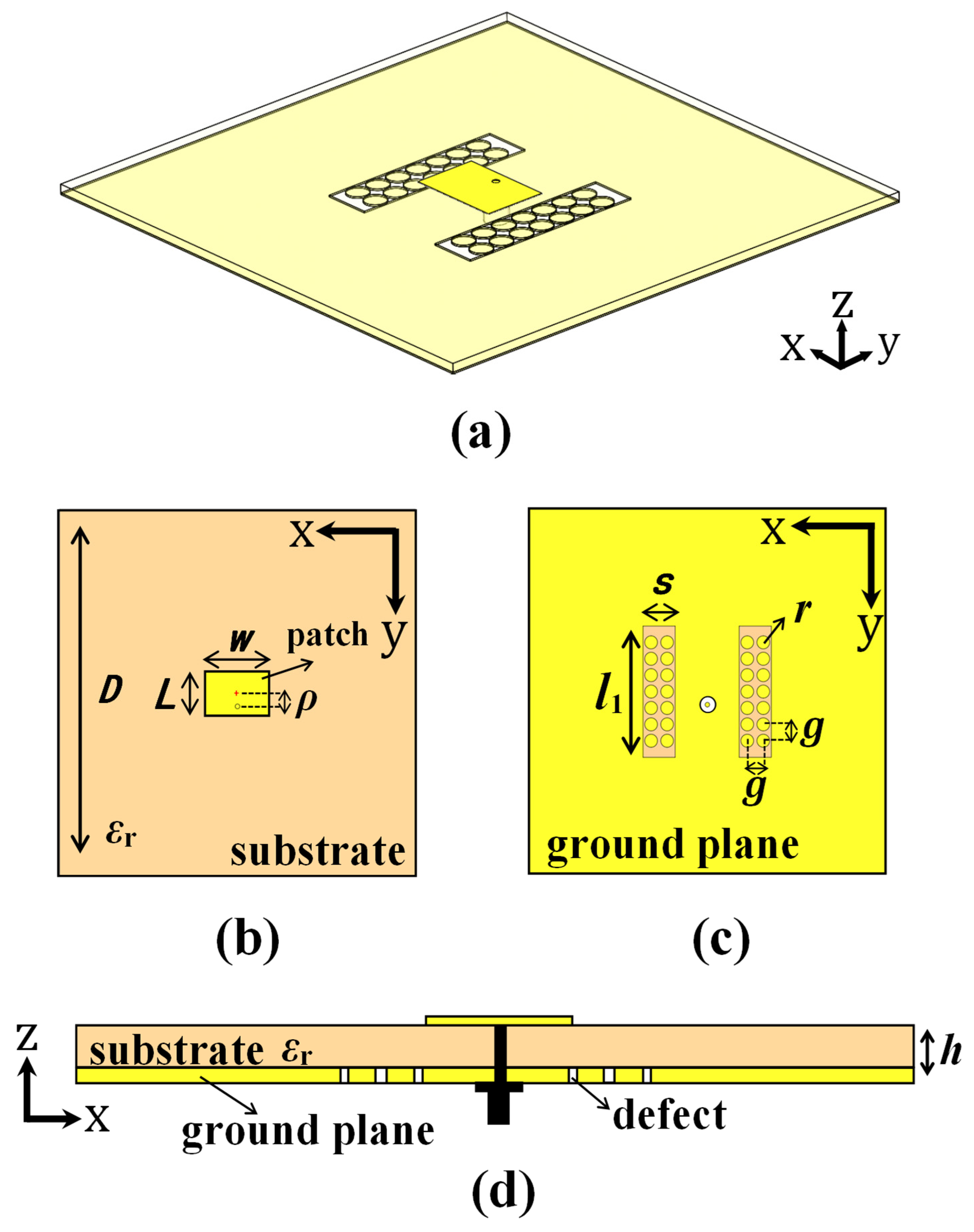
With this above insight, the periodic configuration within a slot-type DGS has been conceived and illustrated in Figure 1. An L × W rectangular patch is placed on a square dielectric substrate of side length D, as shown in Figure 1b. The proposed DGS is constructed by embedding multiple periodically arranged circular metal elements inside the slot-type defect of l1 × s, as shown in Figure 1c. Slot-type defects are introduced into the ground plane adjacent to the non-radiating edges. The two-dimensional photonic crystal configuration is formed by arranging a series of circular metal elements with radius r. PCSs are centrally placed within the rectangular slot defect, with a lattice constant of g = 0.5.

3. Studies Based on Simulated Results

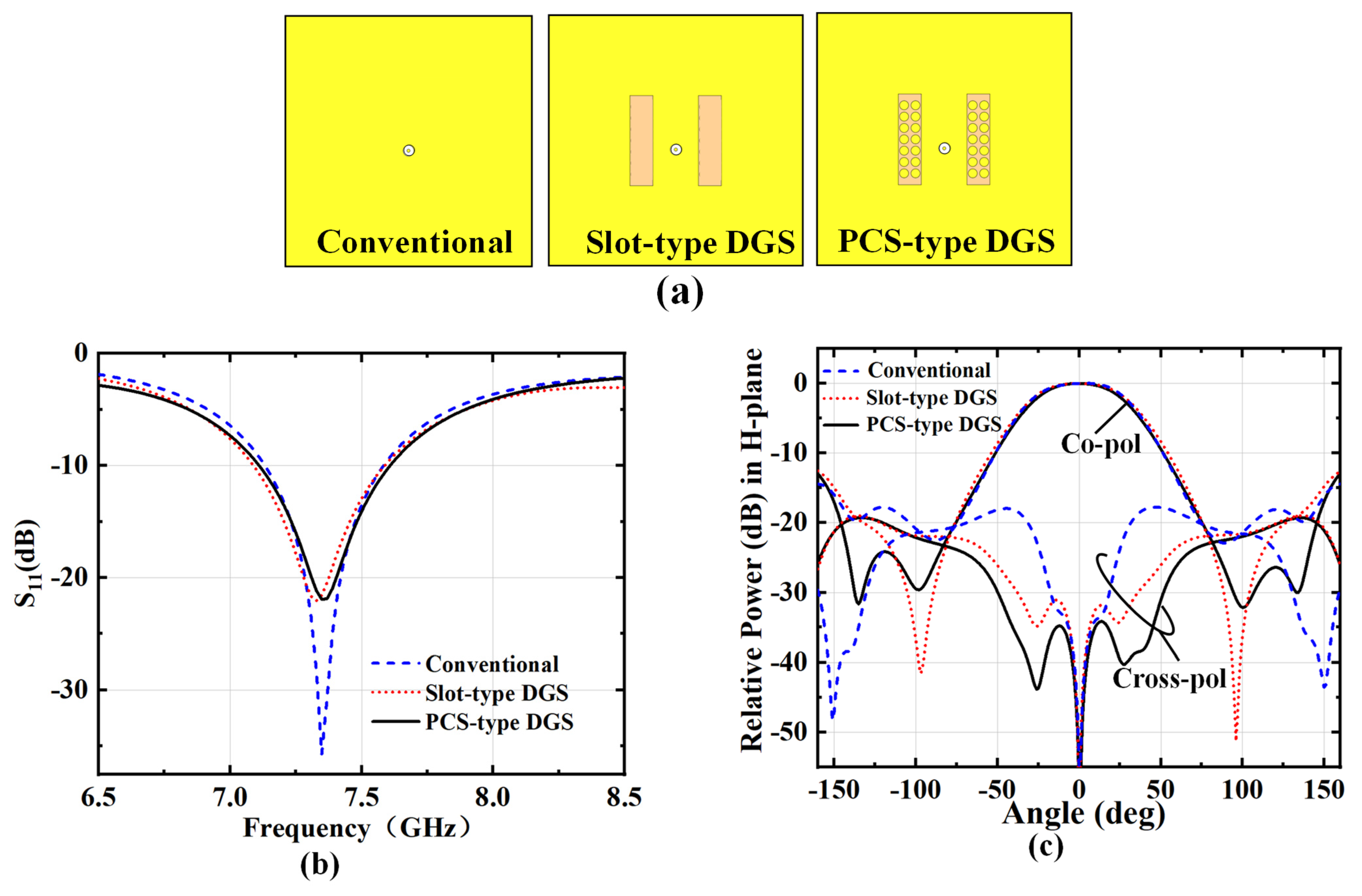
This comprehensive investigation utilizes the finite element method to simulate coax-fed RMAs placed on various types of DGS. To facilitate comparison with the research reported in [14], this section employs an RT5870 substrate with a dielectric constant εr = 2.33 and thickness h = 1.575 mm. Figure 2 compares the H-plane radiation characteristics of the C-band RMAs with W/L = 1.5 based on the conventional ground plane, slot-type, and PCS-type DGS at 7.25 GHz, providing relevant parameters as well. It is noted that all structures depicted in Figure 2a exhibit optimal impedance matching, with operating frequency ranges from 7.15 GHz to 7.6 GHz. The corresponding S11 parameters are displayed in Figure 2b. We focus on the XP radiation suppression in the H-plane, as illustrated in Figure 2c. Within an azimuth range of ±100°, the PCS-type DGS XP level demonstrates a degree of improvement over both conventional ground plane and slot-type DGS. The peak co-cross polarization isolation is enhanced by approximately 20 dB and 10 dB, respectively. The gain values exhibit minimal variation, with 8.61 dBi, 8.54 dBi, and 8.73 dBi.
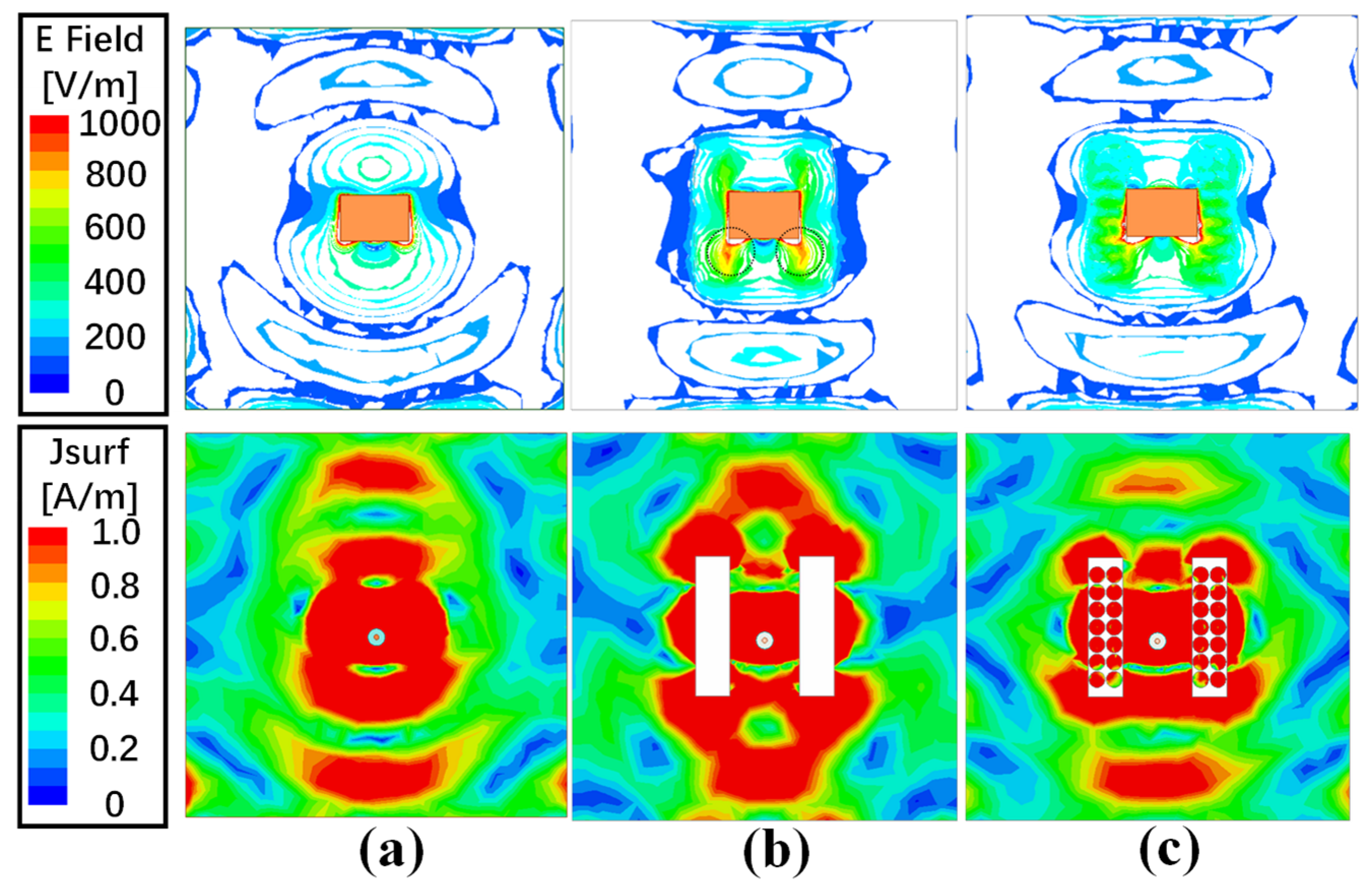
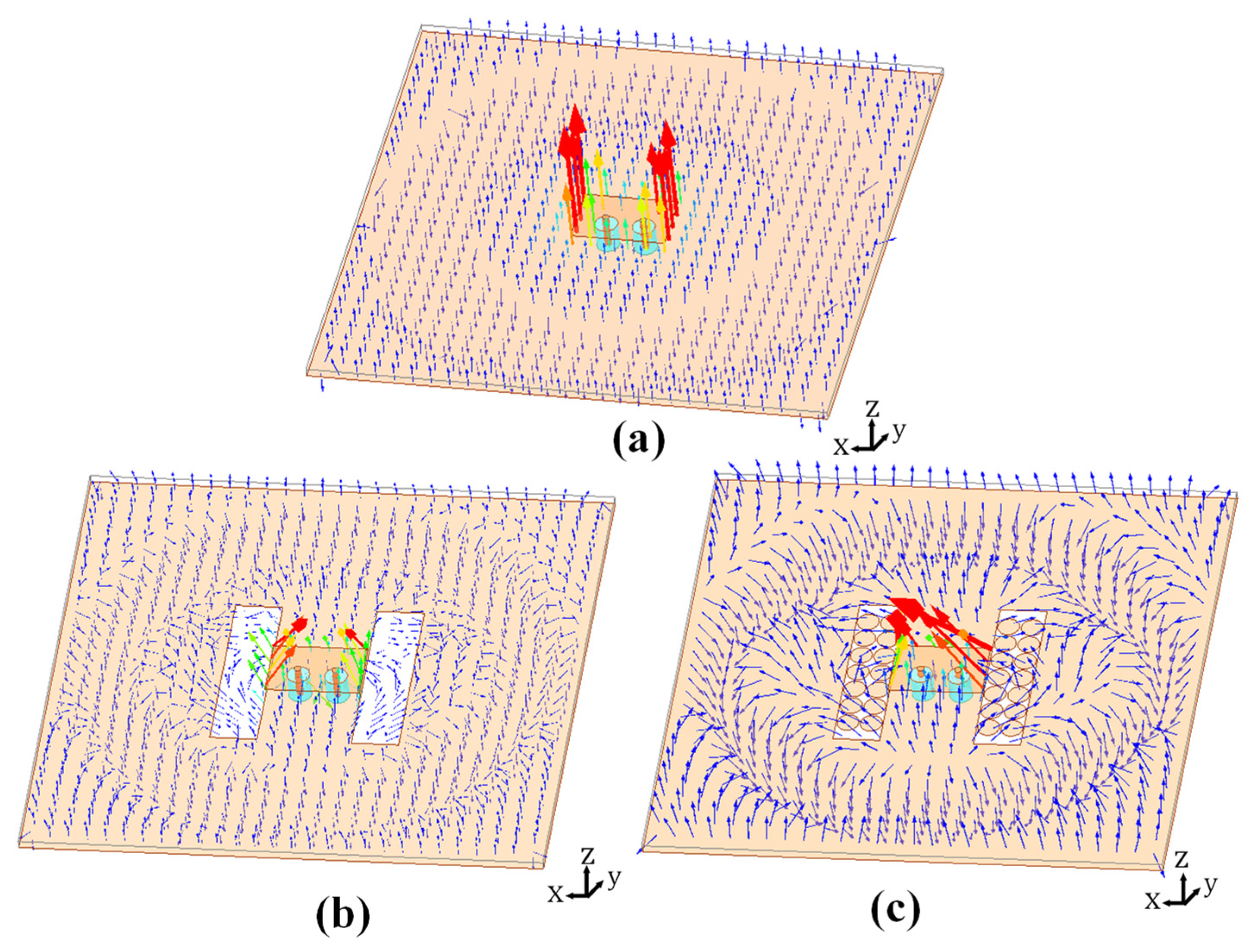
The physical insights underlying the XP behavior of the DGSs are investigated in Figure 3. The RMA electric fields in the substrate and ground plane currents placed on the three ground plane types are displayed. Notably, all plots maintain identical scales of intensity and phase of input excitation. As in previous studies [2,6], the high-order modes of the conventional RMA result in an overall asymmetry of the resonant field below the patch near the probe feed. This asymmetry directly relates to the XP field, as shown in Figure 3a. The slot-type DGS weakens the TM02 mode by introducing slotted-defect interactions with the field, thereby effectively reducing XP radiation. Conversely, the slot-type DGS’s relatively substantial width is not necessarily aligned with its operational frequency. This mismatch generates high field strength at the location delineated by the black circle on the defect edge, thereby disrupting the symmetry of the substrate electric field, as shown in Figure 3b. This phenomenon provides a mechanism for the weakening of XP suppression exhibited by the slot-type DGS when the operating frequency alters. The proposed PCS-type DGS varies the defect field distribution by embedding periodic circular metal elements, as shown in Figure 3c. In the reconfigured field distribution, the resonant field interacts with high-order mode below the defect, while the PCS effectively mitigates undesirable electric fields within the slot defect. This results in superior symmetry of the substrate electric field inside the defect region.
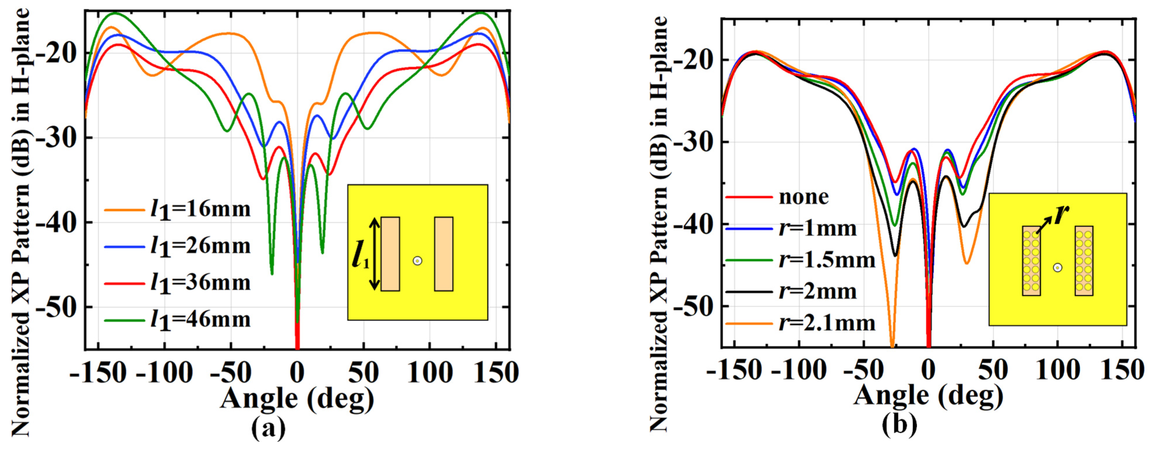
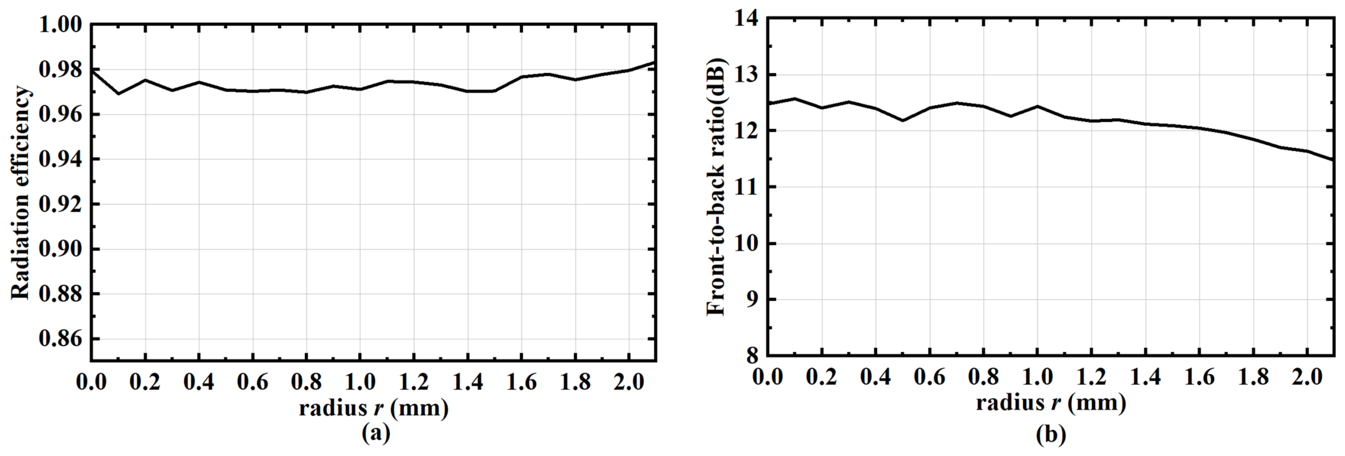
The XP behavior of the RMA with variable lengths of the slot defect is shown in Figure 4a. Within the azimuth range of ±100°, the H-plane XP suppression attains its optimal level at l1 = 36 mm (near the resonant wavelength λ0). Beyond this range, the suppression capability exhibits a decline, with a variation of ±25° to ±45°. It is evident that when the slot length fails to suppress XP across a broader azimuth range, the implementation of a PCS becomes a viable option. As the circular metal elements’ radius r increases, more field couples into the slot from the non-radiating side and disperses into the defect gaps between each metal circle, thereby effectively reducing the XP radiation from TM02 mode, as shown in Figure 5. Accordingly, the XP behavior of the RMA is illustrated with circular metal elements of variable sizes in Figure 4b. The manifestation of XP suppression is observed at r = 1 mm. As r increases, the XP level within ±100° commences its decline, with peak suppression surpassing 20 dB. When the r exceeds 2 mm, the XP level outside the ±50° range demonstrates a slight rise. Therefore, the incorporation of PCS serves to augment the XP suppression capacity of the slot-type DGS over a broad azimuth range. Table 1 presents a summary of PCS design parameters to enhance reproducibility. It has been demonstrated that as the radius r and the metallization area of the slot region increase, the corresponding cross-polarization suppression capability is concomitantly enhanced. It is notable that when the metallization ratio reaches approximately 25%, the rate of improvement begins to accelerate. Concurrently, the antenna gain demonstrates a slight increase with increasing r. In addition, Figure 5 demonstrates the overall impact of the radius on the antenna’s radiation efficiency and front-to-back ratio subsequent to the embedding of the PCS within the slot. As illustrated, radiation efficiency demonstrates an upward trend with increasing radius, while the front-to-back ratio exhibits a downward trend.
The objective of slot-length optimization is to maximize resonance between the slot and the higher-order orthogonal TM02 mode, while the incorporation of PCS aims to further enhance the coupling between the defect and the TM02 mode. The coupling between the microstrip and the slot at ground plane is given by [20],
n = Z 0 m i c r o s t r i p Z 0 s l o t
It is evident that, since Z 0 m i c r o s t r i p remains essentially constant, in order to increase the coupling coefficient n , a further reduction in the slot impedance Z 0 s l o t is required. The attachment of metal plates to the slot results in a reduction in its impedance   Z 0 s l o t , primarily due to two factors: Firstly, the metal plates introduce additional parallel capacitance, thereby increasing the slot’s equivalent admittance and lowering the impedance magnitude. Secondly, the presence of metal plates within the slot modifies its radiation characteristics, thereby reducing the slot’s radiation resistance. Consequently, the PCS-enhanced higher-order orthogonal modes couple with the slot, significantly suppressing cross-polarization radiation from the non-radiating edges of the patch.
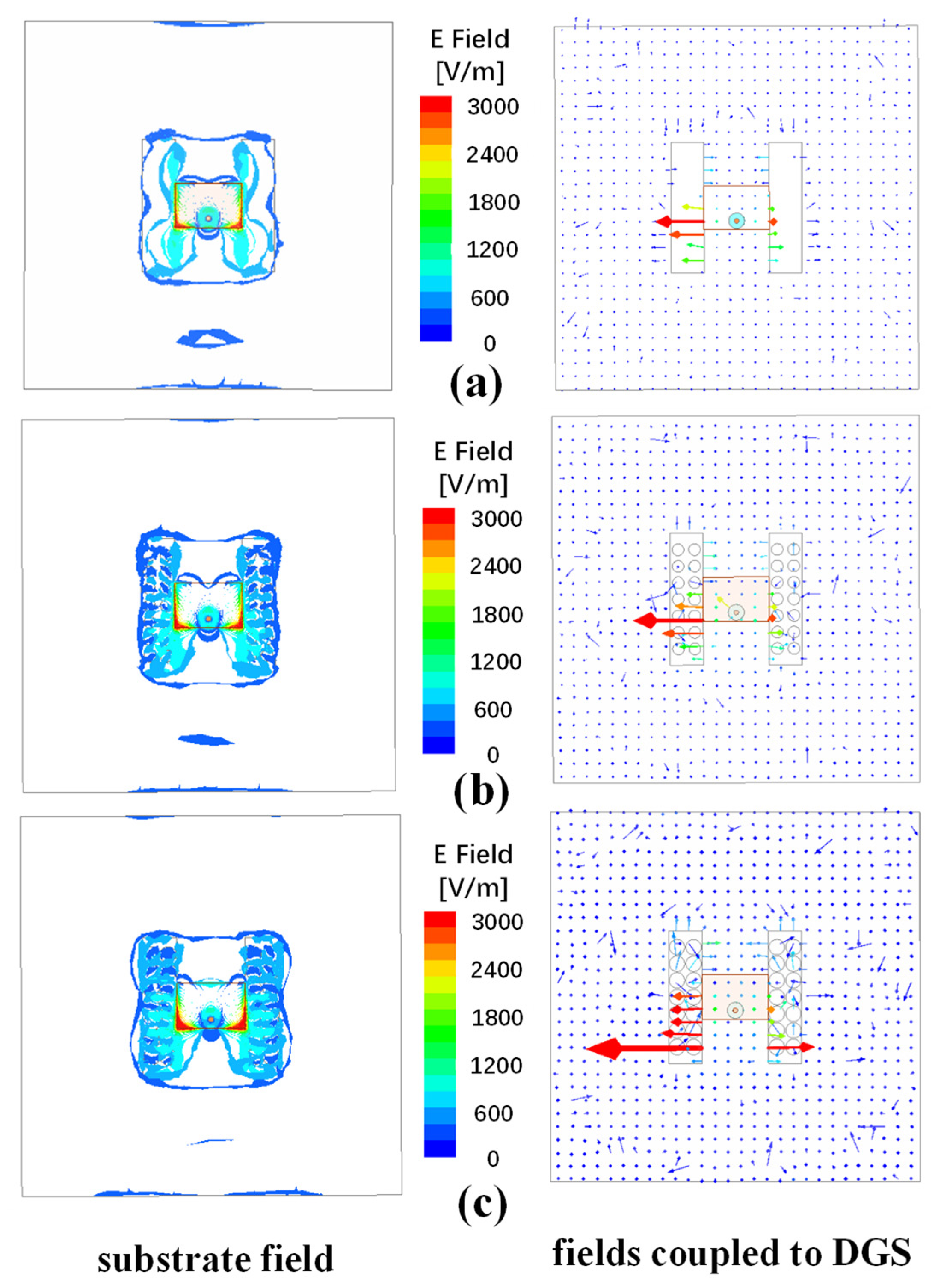
In order to provide an illustration of the working principle of the PCS, Figure 6 shows the simulated electric-field distribution of the slot-type DGS before and after embedding into the PCS at resonance. It is evident that the input excitation intensity and phase are identical in all cases. The figure provides a clear demonstration of the coupling between the electric field and the DGS, with the coupling strength increasing significantly upon PCS integration. The fringing electric fields, which should be concentrated at the patch corners with mutually opposite polarity, partially couple with the DGS. The primary cause of XP radiation attenuation is the DGS’s weakening effect on the Z-polarized corner fields. As demonstrated in Figure 6a, in the conventional slot-type DGS, excessive width results in inadequate edge-field excitation of the defect, consequently yielding a weak and asymmetric DGS electric field. As illustrated in Figure 6b,c, the incorporation of the PCS results in a substantial enhancement of the electric-field strength, attributable to the coupling of the edge field at the patch corner to the DGS. The fringing field uniformly excites the entire defect. This effect is found to intensify as the element radius increases.
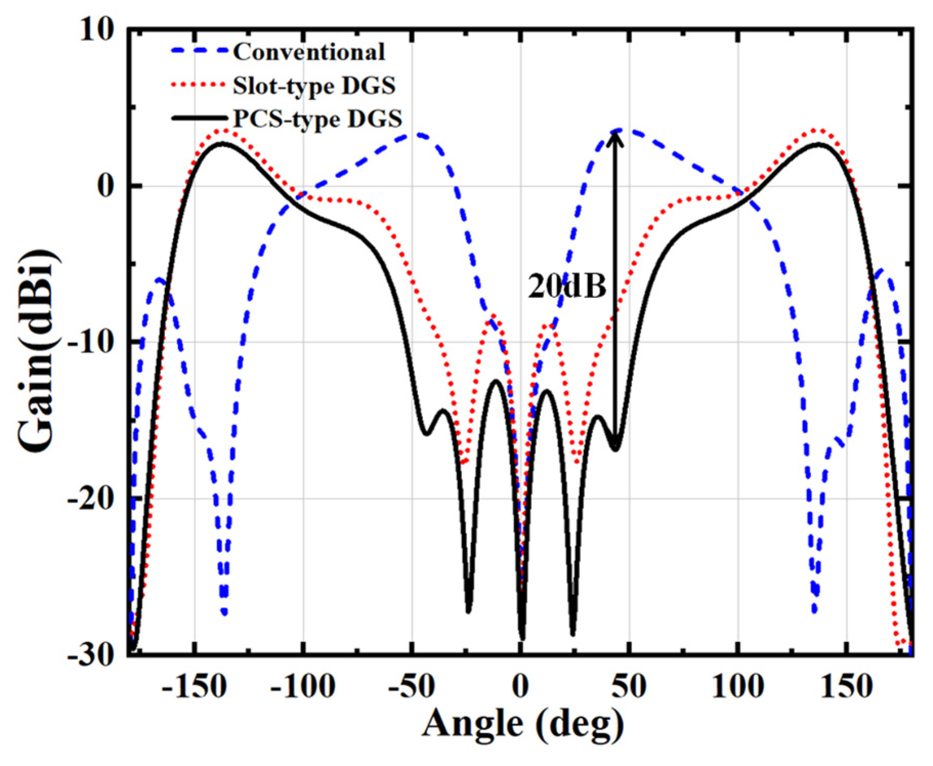
In rectangular microstrip antennas, the primary source of XP generation is the TM02 mode [21]. The excitation of the TM02 mode in the H-plane is facilitated by balanced feeding with identical phase and amplitude. As shown in Figure 7, the TM02 mode fields are displayed both with and without the DGS. The corresponding radiation patterns are illustrated in Figure 8. Figure 7a demonstrates that the vertically polarized-field strength in the proximity of the patch edge exhibits a substantial enhancement. Consequently, peak TM02 radiation is observed around ±50°. Subsequent to the implementation of a slot-type DGS, see Figure 7b, a discernible transition in the prevailing orientation of the overall electric field becomes evident. Following the incorporation of the PCS, see Figure 7c, the fringing field in the patch couples with the PCS-type DGS, causing substantial changes across the entire TM02 mode field. The vertically polarized field in proximity to the patch edge undergoes coupling with the PCS, thereby reducing the vertical field component and inducing a substantial tilt in the electric field orientation. This phenomenon is particularly evident at the corners. In the corresponding radiation pattern, the azimuth of peak gain increases from 50° to 140°, with TM02 mode radiation maintaining a low level over a broader azimuth range, as demonstrated in Figure 8. Research has demonstrated that TM02 radiation exhibits up to 20 dB attenuation. Furthermore, the PCS-type DGS demonstrates a more significant influence on the TM02 mode field in comparison to the slot-type DGS, effectively reducing the z-polarized field component at the patch corner and mitigating broadside radiation generated by TM02 mode.
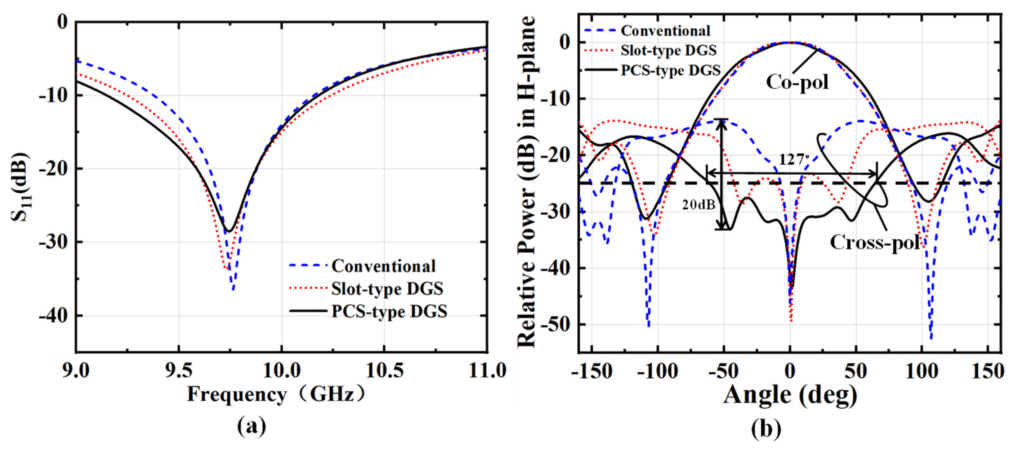
Figure 9 shows another case demonstrating the S11 values and the relative radiation patterns of the X-band RMAs with r = 1.5 in the H-plane at 9.76 GHz. For the purpose of facilitating a more direct comparison with [14], the same RT5870 substrate (εr = 2.33, h = 1.575 mm) is utilized. The impedance bandwidth of the PCS-type DGS is 9.15 GHz–10.18 GHz (bandwidth ratio = 10.65%), representing a 230 MHz improvement over conventional DGSs, as shown in Figure 9a. This phenomenon is attributed to the microstrip patch antenna cavity model, wherein defects below or in proximity to the patch result in a reduction in the Q factor, thereby widening the impedance bandwidth. In Figure 9b, it is evident that the azimuth range for 25 dB XP suppression relative to the peak gain is 127°, representing a 27° improvement to [14]. Moreover, the peak XP suppression has been shown to reach 20 dB. Comparable performance enhancement is also achieved in the C-band, thus providing further validation for the proposed idea.
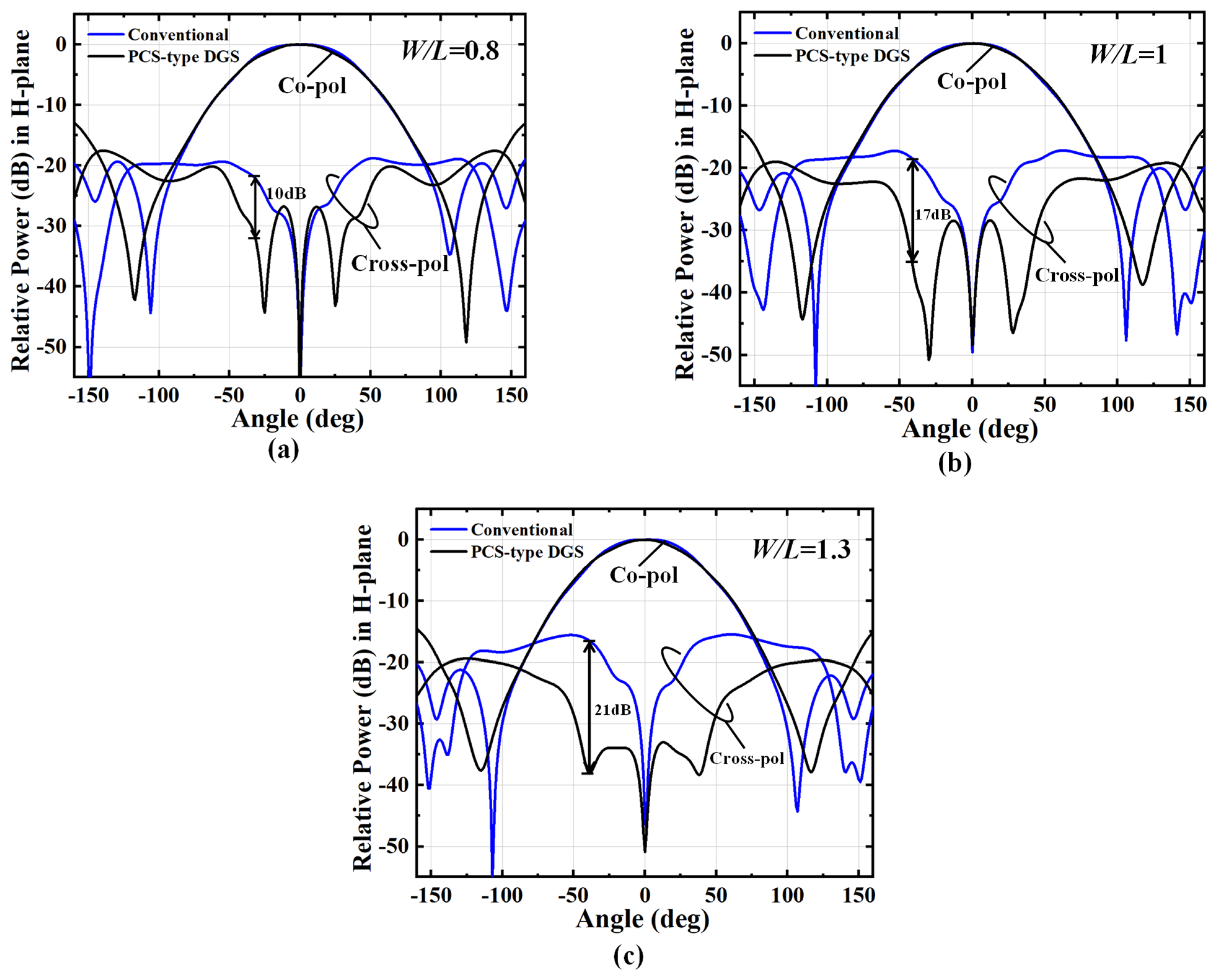
Figure 10 shows results of rectangular and square patches (W/L = 0.8,1, and 1.3) with and without PCS-type DGS. The values of g and r for each case are found to be consistent, and it is demonstrated that the optimum value of l1 increases as W/L rises. With the enhancement of W/L, the peak XP suppression in the H-plane can be elevated from 10 dB to 21 dB. It is also notable that the suppression effect becomes more significant as W/L increases.

4. Experiments and Verification

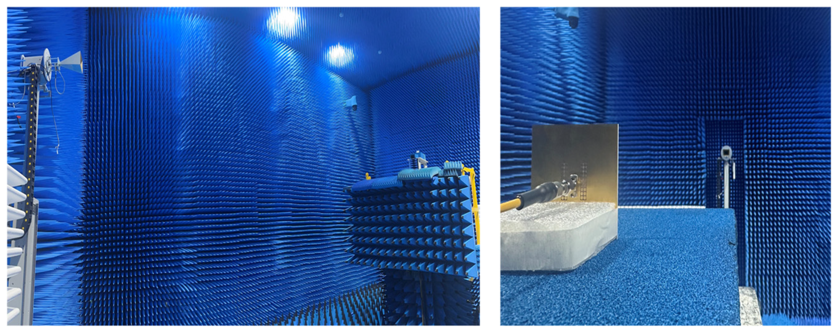
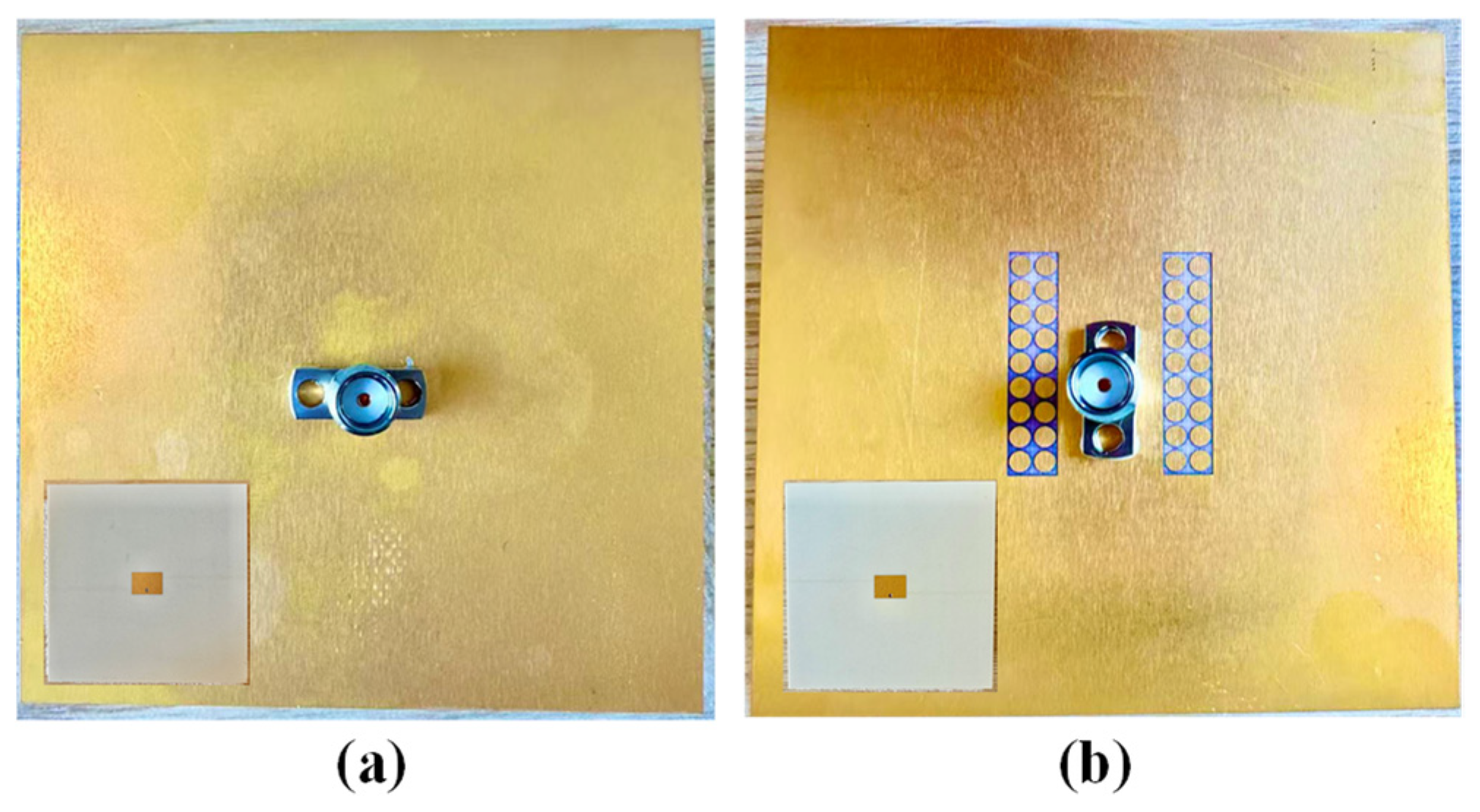
A set of X-band prototypes bearing the conventional ground plane and PCS-type DGS with their relevant parameters is shown in Figure 11. Both prototypes employ rectangular patches with a W/L ratio of 1.4 and RO4350B substrates (εr = 3.48, h = 1.52 mm). The DGS scale is identical to that in Figure 9. And the 0.5 mm diameter SMA probes are installed by conductive adhesive. The prototypes have been measured using the CEYEAR 3674G network analyzer (Ceyear Technologies Co., Ltd. in Qingdao, China) and an automated anechoic chamber, as shown in Figure 12.
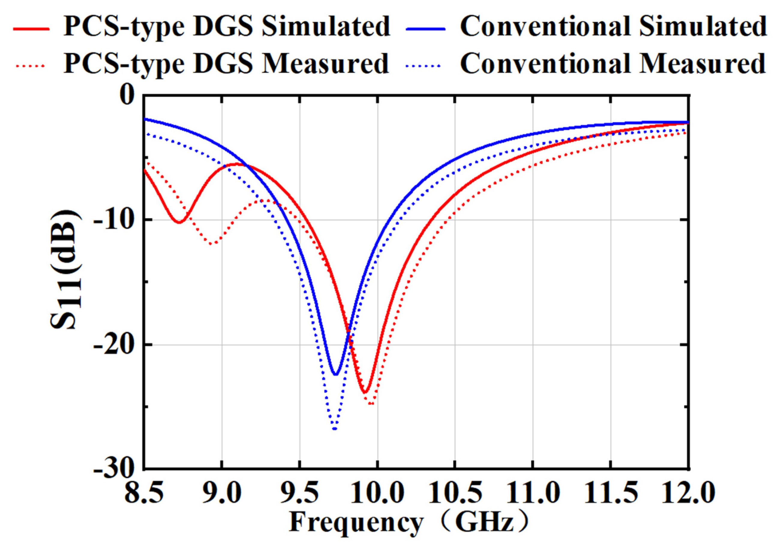
Figure 13 shows the measured and simulated S11 characteristics (bandwidth ratio = 10.25%). The simulated results exhibit a high degree of correlation with the measured results. The introduction of the PCS-type DGS causes a small shift to the right in the resonant frequency, due to reactive loading. This has no considerable effect on the input impedance.
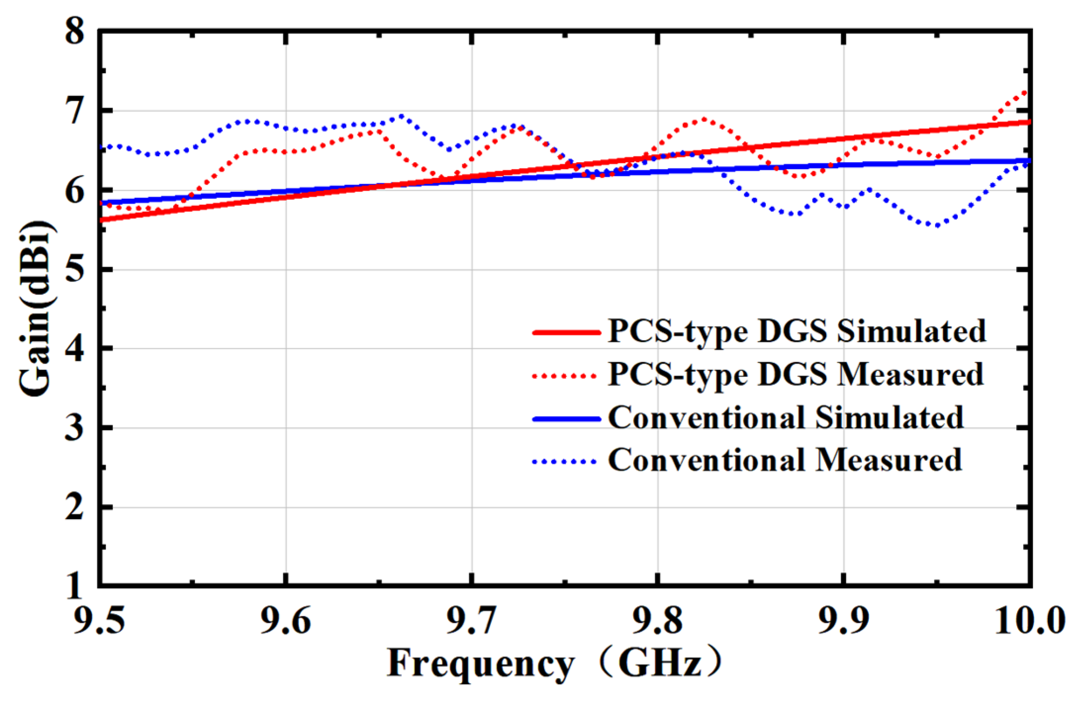
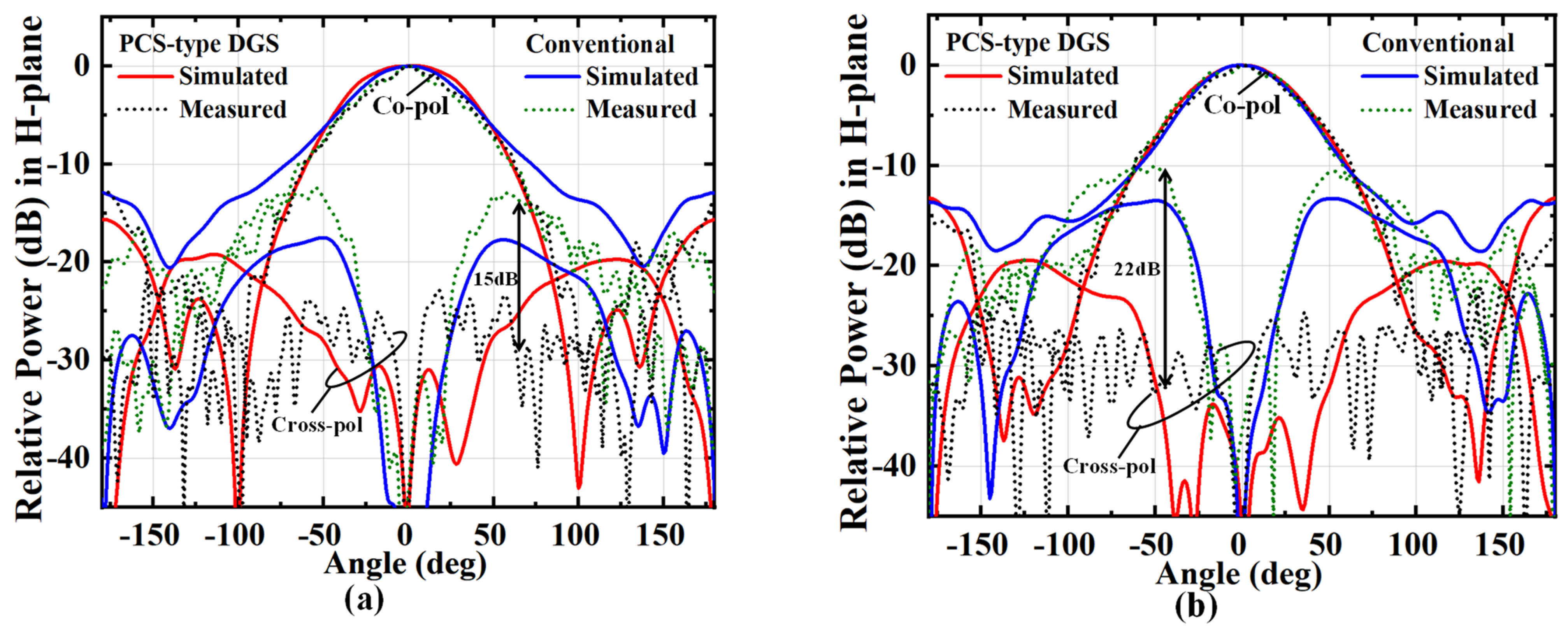
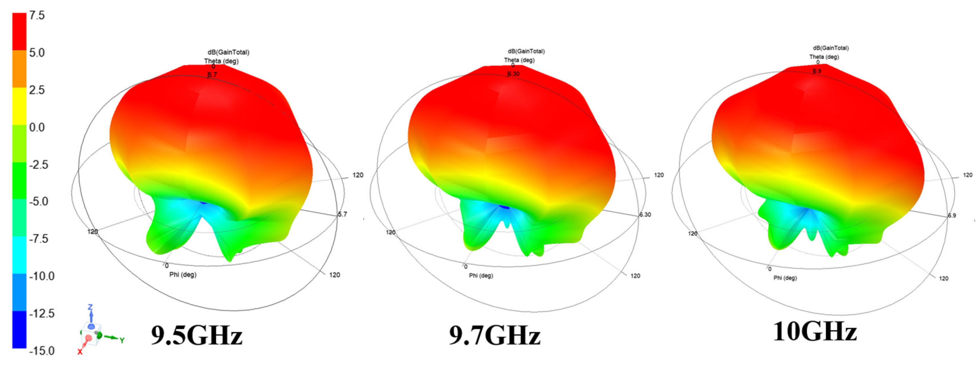
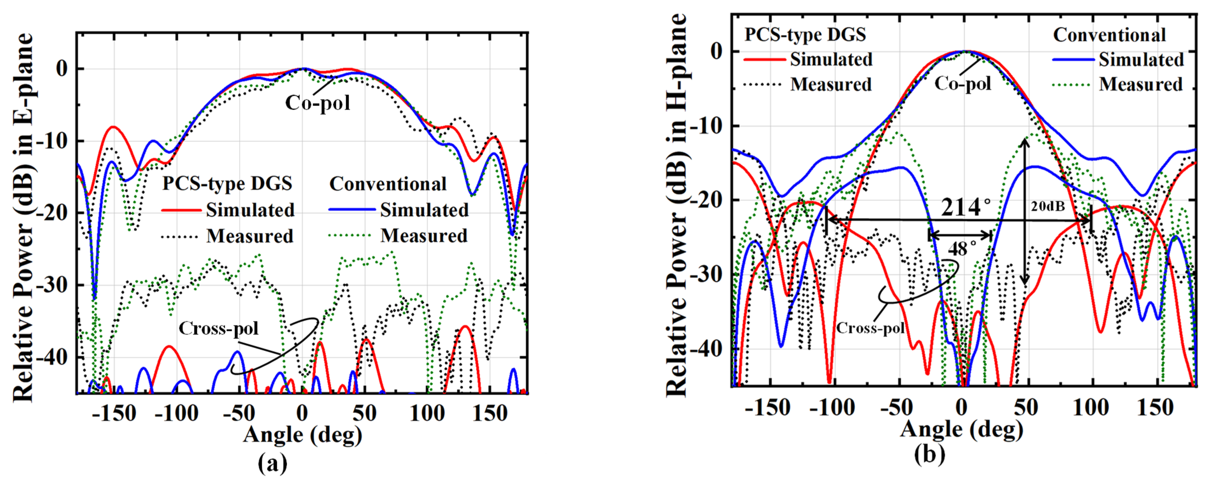
Figure 14 shows the simulated three-dimensional radiation patterns with PCS-type DGS. Figure 15 shows both measured and simulated radiation patterns obtained in two principal planes at the resonant frequency. Figure 15a shows that the PCS-type DGS has no significant effect on radiation patterns in the E-plane, which maintains a low XP level across all azimuth angles. As shown in Figure 15b, the beamwidth of the H-plane co-polarized pattern exhibits a slight decrease in comparison without DGS, which can be attributed to the field redistribution. Concurrently, XP suppression in the H-plane is excellent, yielding peak XP suppression levels of up to 20 dB. Within the 214° azimuth range delineated, only a 10° XP level fails to decrease by 25 dB relative to peak gain. The azimuth range where XP values fall below −25 dB expands from 48° to 204° through the introduction of the proposed PCS-type DGS. Figure 16 shows both measured and simulated results of the variation in gain with frequency. The measured data closely corroborate the simulated predictions. Figure 17 presents the order of consistency of the characteristics over the entire bandwidth. The order of peak suppression varies from the lower band edge to the upper band edge, displaying an approximate range of 15–22 dB.
Table 2 compares the measured RMA XP metrics of the proposed DGS with various representative resonant-type DGSs. In the case of the RMA with a large W/L ratio, the proposed PCS-type DGS exhibits superior capability in maintaining a low XP level across a wide azimuth angle while retaining a lower defect area. Compared to the currently popular asymmetric DGS (L-shape), PCS-type DGS as a symmetric DGS achieves comparable performance while featuring a simpler design.


5. Conclusions

This investigation proposes a novel resonant-type DGS for integrating a slot-type DGS with a PCS to overcome the limitations of the conventional slot-type DGS in improving the polarization purity of RMAs. The design is characterized by its ability to provide stable suppression of XP radiation over a wide azimuth range, while simultaneously optimizing the defect area. The superior characteristics in comparison to earlier designs have been documented.
The fundamental innovation resides in its ability to further enhance the coupling between the fringe field and the DGS compared to the slot-type DGS, thereby overcoming the limitations of the slot structure in controlling the higher-order mode. On one hand, the PCS contributes to the full excitation of the entire slot-type DGS by the patch fringe field. On the other hand, the PCS significantly alters the distribution orientation of the TM02 mode field, weakening the vertically polarized strong fields near the patch edges. Experimental and simulation results validate its efficacy. For X-band RMAs (W/L = 1.4), the azimuth range in which the co-cross polarization isolation exceeds 25 dB is satisfied has been increased by 156° compared to the conventional ground planes, with peak XP suppression of 20 dB. The concept of integrating periodically arranged circular metallic elements within the DGS to form a two-dimensional photonic crystal structure applies to large defect area DGSs, such as the non-proximity DGS [8,9].
Subsequent research will focus on the periodic topological structures of other shapes to enhance polarization purity across the entire azimuth plane. Additionally, the physical concepts from this study will be extended to the design of dual-polarization or circularly polarized antennas.

Author Contributions

Conceptualization, H.M. and J.G.; Methodology, H.M. and J.G.; Software, H.M.; Validation, H.M.; Formal analysis, H.M.; Investigation, H.M.; Resources, H.M.; Data curation, H.M.; Writing—original draft, H.M.; Writing–review & editing, J.G.; Visualization, J.G.; Supervision, J.G.; Project administration, J.G.; Funding acquisition, J.G. All authors have read and agreed to the published version of the manuscript.

Funding

This research received no external funding.

Data Availability Statement

The original contributions presented in this study are included in the article. Further inquiries can be directed to the corresponding author.

Conflicts of Interest

The authors declare no conflict of interest.

References

  1. Hansen, R.C. Cross Polarization of Microstrip Patch Antennas. IEEE Trans. Antennas Propag. 1987, 35, 731–732. [Google Scholar] [CrossRef]
  2. Guha, D.; Kumar, C.; Biswas, S. Defected Ground Structure (DGS) Based Antennas, 1st ed.; Wiley: New York, NY, USA, 2022. [Google Scholar]
  3. Rafidul, S.; Guha, D.; Kumar, C. Sources of Cross-Polarized Radiation in Microstrip Patches: Multiparametric Identification and Insights for Advanced Engineering. IEEE Antennas Propag. Mag. 2023, 65, 92–103. [Google Scholar] [CrossRef] [Scilit]
  4. Guha, D.; Biswas, M.; Antar, Y.M.M. Microstrip Patch Antenna with Defected Ground Structure for Cross Polarization Suppression. IEEE Antennas Wirel. Propag. Lett. 2005, 4, 455–458. [Google Scholar] [CrossRef] [Scilit]
  5. Kumar, C.; Guha, D. Reduction in Cross-Polarized Radiation of Microstrip Patches Using Geometry-Independent Resonant-Type Defected Ground Structure (DGS). IEEE Trans. Antennas Propag. 2015, 63, 2767–2772. [Google Scholar] [CrossRef] [Scilit]
  6. Kumar, C.; Guha, D. Asymmetric Geometry of Defected Ground Structure for Rectangular Microstrip: A New Approach to Reduce Its Cross-Polarized Fields. IEEE Trans. Antennas Propag. 2016, 64, 2503–2506. [Google Scholar] [CrossRef] [Scilit]
  7. Kumar, C.; Guha, D. Asymmetric and Compact DGS Configuration for Circular Patch with Improved Radiations. IEEE Antennas Wirel. Propag. Lett. 2020, 19, 355–357. [Google Scholar] [CrossRef] [Scilit]
  8. Pasha, M.I.; Kumar, C.; Guha, D. Mitigating High Cross-Polarized Radiation Issues over the Diagonal Planes of Microstrip Patches. IEEE Trans. Antennas Propag. 2020, 68, 4950–4954. [Google Scholar] [CrossRef] [Scilit]
  9. Kumar, C.; Pasha, M.I.; Guha, D. Microstrip Patch with Nonproximal Symmetric Defected Ground Structure (DGS) for Improved Cross Polarization Properties over Principal Radiation Planes. IEEE Antennas Wirel. Propag. Lett. 2015, 14, 1412–1414. [Google Scholar] [CrossRef] [Scilit]
  10. Qian, B.; Chen, X.; Zhao, L.; Chen, J.; Kishk, A.A. Reduced Cross Polarization and Backside Radiations for Rectangular Microstrip Antennas Using Defected Ground Structure Combined with Decoupling Structure. IEEE Antennas Wirel. Propag. Lett. 2023, 22, 517–521. [Google Scholar] [CrossRef] [Scilit]
  11. Rafidul, S.; Akinsolu, M.O.; Liu, B.; Kumar, C.; Guha, D. Machine Learning-Assisted Microstrip Antenna Design Featuring Extraordinary Polarization Purity. IEEE Antennas Wirel. Propag. Lett. 2025, 24, 1008–1012. [Google Scholar] [CrossRef] [Scilit]
  12. Rahman, M.M.; Islam, M.S.; Yong, W.H.; Islam, M.T.; Alam, T.; Hakim, M.L.; Al Bawri, S.S.; Moniruzzaman, M. A Wideband Array Antenna with a Novel Matching Circuit and DGS Structure for the Sub 6 GHz Applications. Sci. Rep. 2025, 15, 14756. [Google Scholar] [CrossRef] [Scilit]
  13. Wang, S.; Kong, F.; Li, K.; Du, L. A Planar Triple-Band Monopole Antenna Loaded with an Arc-Shaped Defected Ground Plane for WLAN/WiMAX Applications. Int. J. Microw. Wirel. Technol. 2021, 13, 381–389. [Google Scholar] [CrossRef] [Scilit]
  14. Ghosh, A.; Ghosh, D.; Chattopadhyay, S.; Singh, L.L.K. Rectangular Microstrip Antenna on Slot-Type Defected Ground for Reduced Cross-Polarized Radiation. IEEE Antennas Wirel. Propag. Lett. 2015, 14, 321–324. [Google Scholar] [CrossRef] [Scilit]
  15. Sarkar, T.; Ghosh, A.; Singh, L.L.K.; Chattopadhyay, S.; Sim, C.-Y.-D. DGS-Integrated Air-Loaded Wideband Microstrip Antenna for X- and Ku-Band. IEEE Antennas Wirel. Propag. Lett. 2020, 19, 114–118. [Google Scholar] [CrossRef] [Scilit]
  16. Kumar, C.; Pasha, M.I.; Guha, D. Defected Ground Structure Integrated Microstrip Array Antenna for Improved Radiation Properties. IEEE Antennas Wirel. Propag. Lett. 2017, 16, 310–312. [Google Scholar] [CrossRef] [Scilit]
  17. Gonzalo, R.; De Maagt, P.; Sorolla, M. Enhanced Patch-Antenna Performance by Suppressing Surface Waves Using Photonic-Bandgap Substrates. IEEE Trans. Microw. Theory Tech. 1999, 47, 2131–2138. [Google Scholar] [CrossRef] [Scilit]
  18. Zhou, Y.-Q.; Yu, F.-C.; Shen, T.-G.; Ji, P.-L.; Ge, J.; Gen, J.-F.; Len, J. Investigation of Patch Antennas Based on Embedded Multiple PBG Structure. IEEE Photonics Technol. Lett. 2008, 20, 1685–1687. [Google Scholar] [CrossRef] [Scilit]
  19. Kumar, C.; Raghuwanshi, S.K.; Kumar, V. Graphene-Based Patch Antenna Array on Photonic Crystal Substrate at Terahertz Frequency Band. J. Electromagn. Waves Appl. 2024, 38, 250–263. [Google Scholar] [CrossRef] [Scilit]
  20. Caloz, C.; Okabe, H.; Iwai, T.; Itoh, T. A Simple and Accurate Model for Microstrip Structures with Slotted Ground Plane. IEEE Microw. Wirel. Compon. Lett. 2004, 14, 133–135. [Google Scholar] [CrossRef] [Scilit]
  21. Kumar, C.; Guha, D. Higher Mode Discrimination in a Rectangular Patch: New Insight Leading to Improved Design with Consistently Low Cross-Polar Radiations. IEEE Trans. Antennas Propag. 2021, 69, 708–714. [Google Scholar] [CrossRef] [Scilit]
  22. Kumar, C.; Guha, D. Defected Ground Structure (DGS)-Integrated Rectangular Microstrip Patch for Improved Polarization Purity with Wide Impedance Bandwidth. IET Microw. Antennas Propag. 2014, 8, 589–596. [Google Scholar] [CrossRef] [Scilit]
  23. Zhang, Y.; Han, Z.; Shen, S.; Chiu, C.-Y.; Murch, R. Polarization Enhancement of Microstrip Antennas by Asymmetric and Symmetric Grid Defected Ground Structures. IEEE Open J. Antennas Propag. 2020, 1, 215–223. [Google Scholar] [CrossRef] [Scilit]
  24. Kumar, C.; Guha, D. Defected Ground Structure (DGS) Based Narrow Rectangular Patches: Detailed Investigations with Promising Improvement in Cross-Polar Radiations. In Proceedings of the 2023 IEEE Microwaves, Antennas, and Propagation Conference (MAPCON), Ahmedabad, India, 9–13 December 2023; pp. 1–5. [Google Scholar]
Figure 1. Schematic of the RMA with PCS-type DGS. (a) Isometric view. (b) Top view. (c) Bottom view. (d) Cross-sectional view.
Electronics 15 00677 g001
Figure 2. Investigation of C-band RMAs with different configurations of DGS. (a) Diagrammatic view, (b) simulated reflection coefficient, (c) corresponding simulated H-plane relative radiation patterns. W = 18, L = 12, ρ = 3.6, l1 = 36, s = 9, g = 4.5, r = 2, D = 100, εr = 2.33. (all dimensions in millimeters).
Electronics 15 00677 g002
Figure 3. Simulated electric field in the substrate (top view) and ground plane currents distribution at 7.25 GHz: (a) conventional ground plane, (b) slot-type DGS, (c) PCS-type DGS. (in color diagram: red indicates the strongest fields, and blue means the weakest one).
Electronics 15 00677 g003
Figure 4. Simulated H-plane normalized XP patterns of C-band rectangular patches with slot-type DGS and PCS-type DGS for different parameters. (a) Defect length l1. (b) Circular metal elements radius r under l1 = 36 mm.
Electronics 15 00677 g004
Figure 5. Simulated radiation performance versus radius r. (a) Radiation efficiency. (b) Front-to-back ratio.
Electronics 15 00677 g005
Figure 6. Simulated electric field in the substrate versus r: (a) slot-type DGS, (b) r = 1.6 mm, (c) r = 2.1 mm.
Electronics 15 00677 g006
Figure 7. Investigation with the TM02 mode fields; view of the E-fields. (a) Without DGS. (b) With slot-type DGS. (c) With PCS-type DGS.
Electronics 15 00677 g007
Figure 8. Radiation patterns in X–Z plane of the antennas as in Figure 6.
Electronics 15 00677 g008
Figure 9. Investigation of X-band RMAs with different configurations of DGS. (a) Simulated reflection coefficient, (b) corresponding simulated H-plane relative radiation patterns. W = 13.5, L = 9, ρ = 3.4, l1 = 21, s = 4.6, g = 2.3, r = 1.1, D = 80, εr = 2.33. (All dimensions in millimeters).
Electronics 15 00677 g009
Figure 10. Simulated H-plane relative radiation patterns of X-band RMAs with different W/L values. (a) W = 7.2, L = 9, ρa = 1.9, ρb = 1.9, l1 = 26, (b) W = 9, L = 9, ρa = 2.2, ρb = 2.5, l1 = 25, (c) W = 11.7, L = 9, ρa = 2.8, ρb =3, l1 = 23. Other parameters as in Figure 9. (All dimensions in millimeters).
Electronics 15 00677 g010
Figure 11. Photographs of two prototypes: (a) conventional, (b) PCS-type DGS. W = 10, L = 7.1, ρa = 2.2, ρb = 2.6, l1 = 21, s = 4.6, g = 2.3, r = 1, D = 65. (All dimensions in millimeters).
Electronics 15 00677 g011
Figure 12. Photographs of the test environment.
Electronics 15 00677 g012
Figure 13. Measured and simulated reflection coefficient versus frequency with and without PCS-type DGS. Parameters as in Figure 11.
Electronics 15 00677 g013
Figure 14. Simulated three-dimensional radiation patterns with PCS-type DGS. Parameters as in Figure 11.
Electronics 15 00677 g014
Figure 15. Measured and simulated normalized radiation patterns of X-band RMAs without DGS and with PCS-type DGS. (a) E-plane. (b) H-plane. Parameters as in Figure 11.
Electronics 15 00677 g015
Figure 16. Measured and simulated gain versus frequency. Parameters as in Figure 11.
Electronics 15 00677 g016
Figure 17. Measured and simulated normalized radiation patterns in H-plane at the band edge frequency (S11 = −10 dB). (a) Lower frequency side. (b) Higher frequency side. Parameters as in Figure 11.
Electronics 15 00677 g017
Table 1. Summary table of PCS design parameter.
r (mm)Metallization Area Ratio 1 (%)Peak XP Suppression (dB) 2Gain (dBi)
0.20.510.38.3
0.42.211.88.4
0.64.911.88.4
0.88.7128.3
113.612.28.4
1.219.514.28.5
1.426.614.68.5
1.634.817.78.5
1.843.917.98.6
254.323.38.6
2.159.923.38.6
1 Ratio of the area of multiple periodic circular metal to the area of the slot. 2 Peak suppression of cross-polarization in the H-plane with PCS-type DGS compared to without DGS.
Table 2. Comparison of different types of DGS and measured performance of RMAs.
DGS TypeFrequency
(GHz)
Patch Size
(W/L)
Angular Width in H-Plane with XP 25 dB Below the Peak Gain (°)Peak XP Suppression (dB)Peak
Gain
(dBi)
Folded [22]10.101.68610–157
Slot [14]9.801.510010–15-
Linear [5]10.151.615015–186.5
L-shape [6]10.101.6190157
Grid [23]3.571.616815–206.6
‘] [’ -shape [24]9.910.880286.1
Present9.731.420415–226.7
Disclaimer/Publisher’s Note: The statements, opinions and data contained in all publications are solely those of the individual author(s) and contributor(s) and not of MDPI and/or the editor(s). MDPI and/or the editor(s) disclaim responsibility for any injury to people or property resulting from any ideas, methods, instructions or products referred to in the content.