

Article

Neutron-Induced Ionizing Effects at High Flux in Deep Submicron CMOS Integrated Circuits

1
Institute of Electronic Engineering, China Academy of Engineering Physics, Mianyang 621999, China
2
College of Physics, Jilin University, Changchun 130012, China
3
Institute of Nuclear Physics and Chemistry, China Academy of Engineering Physics, Mianyang 621999, China
*
Authors to whom correspondence should be addressed.
Electronics 2026, 15(20), 4585; https://doi.org/10.3390/electronics15204585
Submission received: 10 September 2026 / Revised: 4 October 2026 / Accepted: 6 October 2026 / Published: 9 October 2026

Abstract

Neutron radiation causes ionizing-energy loss (IEL) and non-ionizing-energy loss (NIEL) in materials, and the deposition of ionizing-energy excites electron–hole pairs, causing ionizing radiation effects in semiconductor devices. Reactor neutron-irradiation experiments on 130 nm CMOS integrated circuits were carried out, and it was found that secondary ionization induced a local latch-up effect that would occur in 130 nm CMOS integrated circuits when the neutron fluence reached 1010–1011/cm2 under high-reactor-neutron-flux irradiation. Geant4 was used to calculate IEL and NIEL of 1–14 MeV neutrons in the sensitive region of a 130 nm transistor and IEL collected the charge generated by IEL under the neutron spectrum conditions of the reactor. The range of the sensitive region, ionizing-charge distribution and charge-collection mechanism inside the device were analyzed in depth by combining experiment and simulation. The results provide an important reference for the study of the radiation effects of high neutron-flux in CMOS devices with smaller feature sizes.

1. Introduction

Cosmic rays pass through the atmosphere and react with oxygen and nitrogen nuclei to produce neutrons, whose energy distribution ranges from MeV to GeV, and whose flux is related to latitude and height [1]. The neutron-energy distribution range of the reactor during steady-state operation is keV~14 MeV, and the neutron-flux is mainly 106~109 n/cm2·s [2]. In the field of neutron-radiation effects on semiconductor devices, previous research has mainly concentrated on neutron-displacement damage effects and high-energy neutron-induced single-event effects (SEE) [1,2,3,4,5,6,7,8]. As the process size of semiconductor devices continues to decrease, the critical charge required by the turnover of integrated circuit nodes (from 1 to 0 or from 0 to 1) continues to decrease. Many studies have been carried out on the single-particle effect of a neutron at home and abroad [9,10,11,12,13,14]. Among the existing research results, most studies on single-event latch-up (SEL) have been observed under high-energy neutron irradiation. For example, J.R. Schwank studied the single-particle effect of seven SRAM devices (process size ranging from 0.14 μm to 0.35 μm) under WNR radiation environment (the highest energy can reach 800 MeV), and only two devices showed a locking effect, with locking cross-sections ranging from 10−11 to 10−10 cm2 [15]. E. Mand studied six gate arrays with process sizes between 0.7 μm and 1.25 μm in WNR radiation environment, and only two of them observed SEL, with locking rates of 3 × 10⁻¹¹/dev and 7 × 10⁻¹²/dev, respectively [16]. Jake Tausch’s research showed that a 130 nmSRAM micro latch-up effect was measured under LAMSCE neutron spectrum [17]. And the research work of Guo Xiaoqiang et al. shows that the turnover cross-section of a 130 nm bulk silicon microprocessor is about (1 × 10⁻¹⁶~1 × 10⁻¹⁴) cm2 [14]. The above studies mainly focus on the single-particle effect induced by the secondary ionization of a single neutron. However, the results of high-flux neutron-irradiation experiments carried out by our research group show that the turnover cross-section of 130 nm bulk silicon microprocessor is larger than 5.6 × 10⁻¹² cm2, that is, the turnover cross-section of 130 nm bulk silicon microprocessor is larger under the condition of high-flux neutron irradiation, and there is an obvious neutron-flux correlation. Moreover, the existing physical mechanism of neutron single-particle effect cannot explain this phenomenon, so it is speculated that the turnover of integrated circuit nodes under the condition of high-flux neutron irradiation may be caused by the synergistic effect of multiple secondary ionization of neutrons. In addition, the recognition of the ionization effect of high-flux neutron is an important problem for the reliable operation of instruments and equipment in the reactor radiation environment.
In order to explore the radiation effect mechanism of integrated circuits under the irradiation of high-flux neutrons, high-flux neutron-irradiation experiments of deep submicron (130 nm) CMOS integrated circuits were carried out in this paper. The ionizing-energy loss (IEL), non-ionizing-energy loss (NIEL) and collected charges of 1–14 MeV neutrons in the sensitive region of 130 nm transistors are calculated by Geant4. The mechanism of high-flux neutron-irradiation effect is discussed by combining experimental data and simulation results.

2. Experimental Design and Simulation Model

2.1. Experimental Design

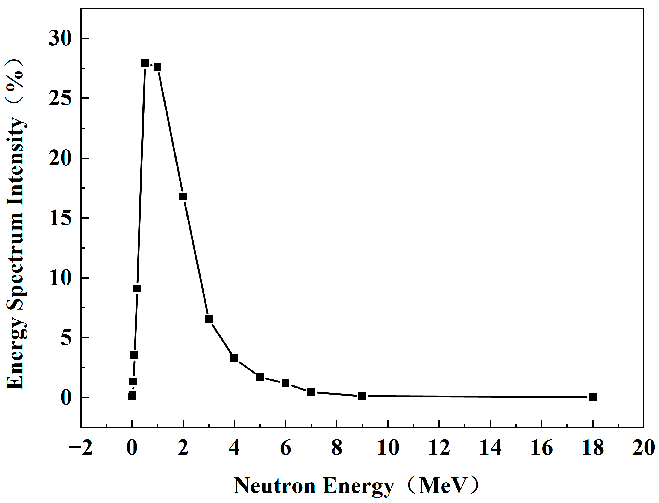
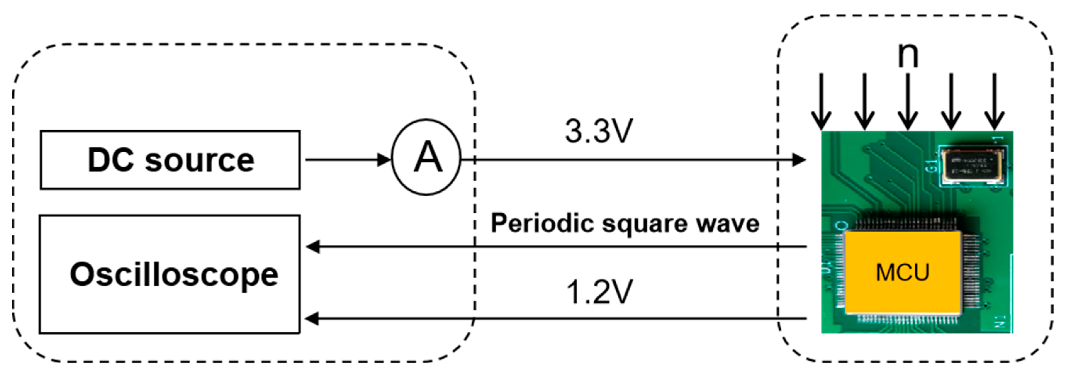
A 130 nm bulk silicon CMOS microprocessor was irradiated with high neutron-flux in a reactor. The neutron-energy spectrum of the reactor is shown in Figure 1. The energy distribution range is keV ~14 MeV, and the average energy is about 1 MeV. The test circuit consists of a microprocessor, a 16 MHz crystal oscillator and some necessary resistance capacitors. The signal generated by the crystal oscillator is input to the microprocessor, which then outputs a 50 MHz periodic square-wave signal and a 1.2 V level signal. According to the available test data, the parameters and functions of the 16 MHz crystal oscillator and resistance capacitance do not change significantly within the range of neutron injection and total dose of accompanying ionization in this test, which can be considered to have no influence on the test results of the microprocessor. The long-line in situ dynamic testing method was used to carry out the irradiation test, as shown in Figure 2. The test circuit was placed at a certain position away from the sphere of the reactor. The two sets of samples in this experiment adopted different neutron-flux. The neutron-flux of sample #1 was 4 × 10⁹ n/cm2•s, and that of sample #2 was 4.4 × 10⁹ n/cm2•s. DC voltage regulator, ammeter, oscilloscope and other test equipment are placed in the test room far away from the radiation source. These test equipment and the sample circuit are connected with about 40 m of cable. Through the comprehensive analysis of the above parameters and functions, the radiation effect of the test circuit is judged.

2.2. Simulation Model of Neutron-Energy Deposition

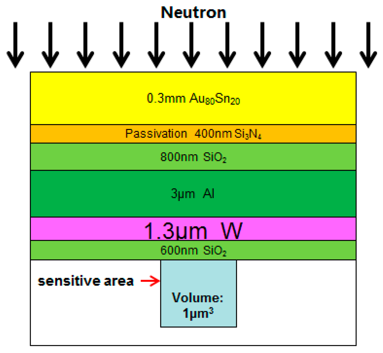
The Monte Carlo method has been used to calculate the energy deposition of neutrons in materials [2,18,19,20]. In this paper, Geant4 is used to calculate the energy deposition of the neutron-incident transistor. A simplified three-dimensional physical model is established based on 130 nm transistors, as shown in Figure 3. The top layer is the packaging cover material (Au80Sn20). The materials inside the microprocessor from top to bottom are Si3N4 (400 nm), SiO2 (800 nm), AL (3 μm), W (1.3 μm), SiO2 (600 nm), and the volume of the sensitive area of Si. And the sensitive region volume of Si is set to 1 μm3. The radiation source is a unidirectional planar neutron source with a radius of 10 μm.
The physical processes involved in the interaction between neutrons and substances in the simulation mainly include elastic scattering, non-elastic scattering, and a series of nuclear reaction processes (including (n, a), (n, p), neutron capture reaction, nuclear fission reaction, etc.). Neutrons collide with nuclei, causing displacement of lattice atoms. The lattice atoms are called Primary Knock-on Atoms (PKAs). If PKA has higher energy, it will continue to collide with other Secondary Knock-on Atoms (SKAs), causing more atomic displacement.
To calculate this “cascading process” of displacement is to simulate the statistical behavior of a large number of PKAs and SKAs. IEL and NIEL of neutrons in sensitive regions were counted by tracking PKAs. The recording method of a physical quantity is as follows: PKA is generated by neutron incident; during the collision between PKA and target material, the ionizing-energy loss (IEL) is equal to the ionization-preventing section multiplied by the track length; the collision between PKA and the nucleus generates SKA, which will generate vacancy, phonon and ionization. The specific energy distribution of each part of SKA is calculated by the improved Kinchin–Pease model [21]. Continue tracking the PKA until it escapes or its energy falls below the truncation energy. Due to the strong penetration ability of neutrons, the material thickness in the calculation model is much smaller than the neutron free path, so the NIEL and IEL in silicon are approximately evenly distributed.

3. Results and Discussion

3.1. Discussion of Experimental Results

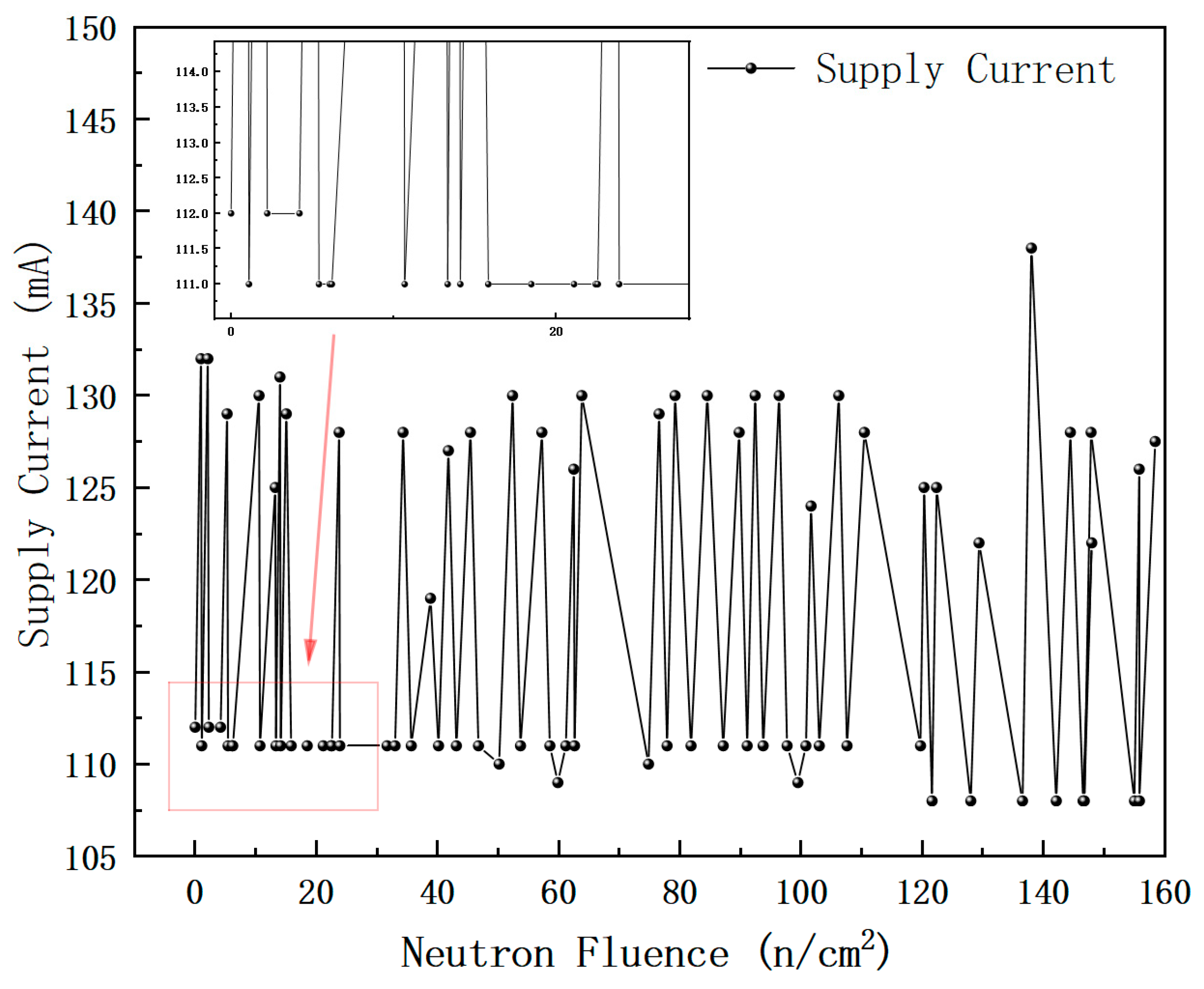
Before the irradiation test, the working current ICC of the test circuit is 110 mA. The main phenomena of the test circuit during the irradiation test are shown in Table 1. Most of the ICC jumps are current increases, which are concentrated in the range of 12 mA to 21 mA; a few jumps of ICC are current reduction, and the reduction is concentrated in 1~2 mA. Each current jump is accompanied by the interruption of the square-wave signal of the microprocessor, which requires power-off and restart to recover. The change in ICC signal with neutron fluence is shown in Figure 4. Although the neutron-flux of sample #1 and sample #2 are different, the neutron fluence experienced between the two function interruptions is roughly the same, mainly concentrated in (0.5~3) × 1011 n/cm2. When the neutron fluence reaches 1.6 ×10¹³ n/cm2, a total of 45 current jumps with function interruption were detected in sample #1, including 36 current increase jumps and 9 current decrease jumps; a total of 49 current jumps with function interruption were detected in sample #2, including 39 current jumps with current increase and 10 current decreases. Since the test does not use automatic current monitoring to monitor the number of current jumps, each time the current jump and function interruption occur, the power is cut off manually, and the waiting time is about 15 s before the power is restored. It is expected that the actual number of current jumps is much greater than the above count.
The microprocessor uses a typical bulk silicon CMOS process, which does not strongly rely on minority carrier lifetime and is insensitive to the reduction in minority carrier lifetime caused by neutron-displacement damage. Combined with the relevant test data of previous bulk silicon CMOS circuits, its level of resistance to the neutron-displacement effect is far greater than 1013 n/cm2. The normal function and working current of the microprocessor can be restored by power-off and restart, and the above abnormal phenomena will not occur in the microprocessor after the neutron-irradiation experiment. The above analysis shows that the phenomenon of microprocessors in this neutron-irradiation experiment is not the displacement damage effect caused by neutrons, but the secondary ionizing radiation effect of neutrons. The microprocessor suffers a functional interruption of a square-wave output, accompanied by a current jump, and functional restart cannot be achieved without power cycling. Therefore, it can be inferred that the functional interruption of the microprocessor is not caused by single-event transient (SET) or single-event upset (SEU). Based on the above, it can be inferred that the localized latch-up effect caused by the secondary ionization of neutrons may be the underlying cause.
Based on the average neutron fluence experienced by the microprocessor between two latches, it is estimated that the actual possible number of latches is about 60 times for sample #1 and 67 times for sample #2, from which we can obtain that the neutron partial locking section of the microprocessor circuit in the dynamic operation mode is about 3.75 × 10⁻¹² cm2 for sample #1 and 4.19 × 10⁻¹² cm2 for sample #2.
Based on the inferred average neutron fluence endured by the microprocessor between two latch-ups (calculated at 15 s per operation), the actual possible number of latch-up events is approximately 60 times (with a data error of 20%) for sample #1 and 67 times (with a data error of 20%) for sample #2. From this, the neutron single-event latch-up (SEL) cross-section of the microprocessor circuit under the dynamic operating mode can be derived as approximately 3.75 × 10⁻¹² cm2 and 4.19 × 10⁻¹² cm2.

3.2. Simulation Results of Neutron-Energy Deposition

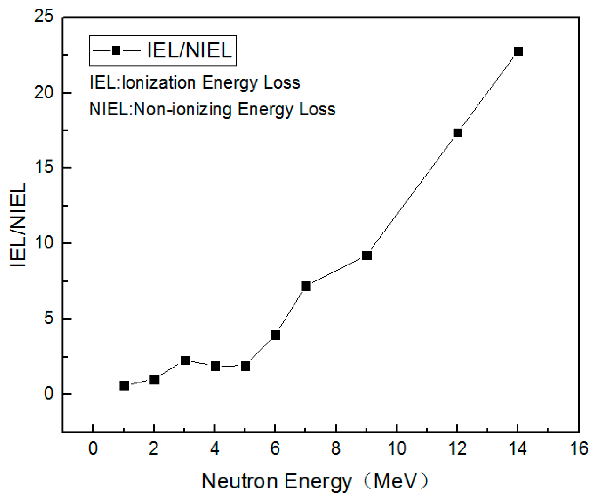
Neutron ionization is mainly produced by atomic recoil and the reaction of secondary charged particles. IEL and NIEL are close when the neutron energy is less than 5 MeV. When the neutron energy is greater than 5 MeV, IEL increases significantly compared to NIEL, becoming a major contributor to the total energy loss. Figure 5 shows the calculated IEL/NIEL energy-deposition ratio of 1–14 MeV neutrons in the sensitive region. Studies by J. Baggio et al. showed that in semiconductor devices with characteristic sizes smaller than 0.25 micron, single-particle turnover caused by 4 MeV and 6 MeV neutrons is mainly due to the contribution of (n, α) nuclear reactions [9]. It takes 3.6 eV of energy to ionize electron–hole pairs in silicon. When the energy deposition of a sensitive unit in a silicon device is E, the total charge collected can be expressed as
Q = e · ∆ E ( MeV ) 3.6 ( eV ) = 1000 × ∆ E ( MeV ) 22.5 ( fC )
where e is the basic charge of 1.602 × 10⁻¹⁹ C.
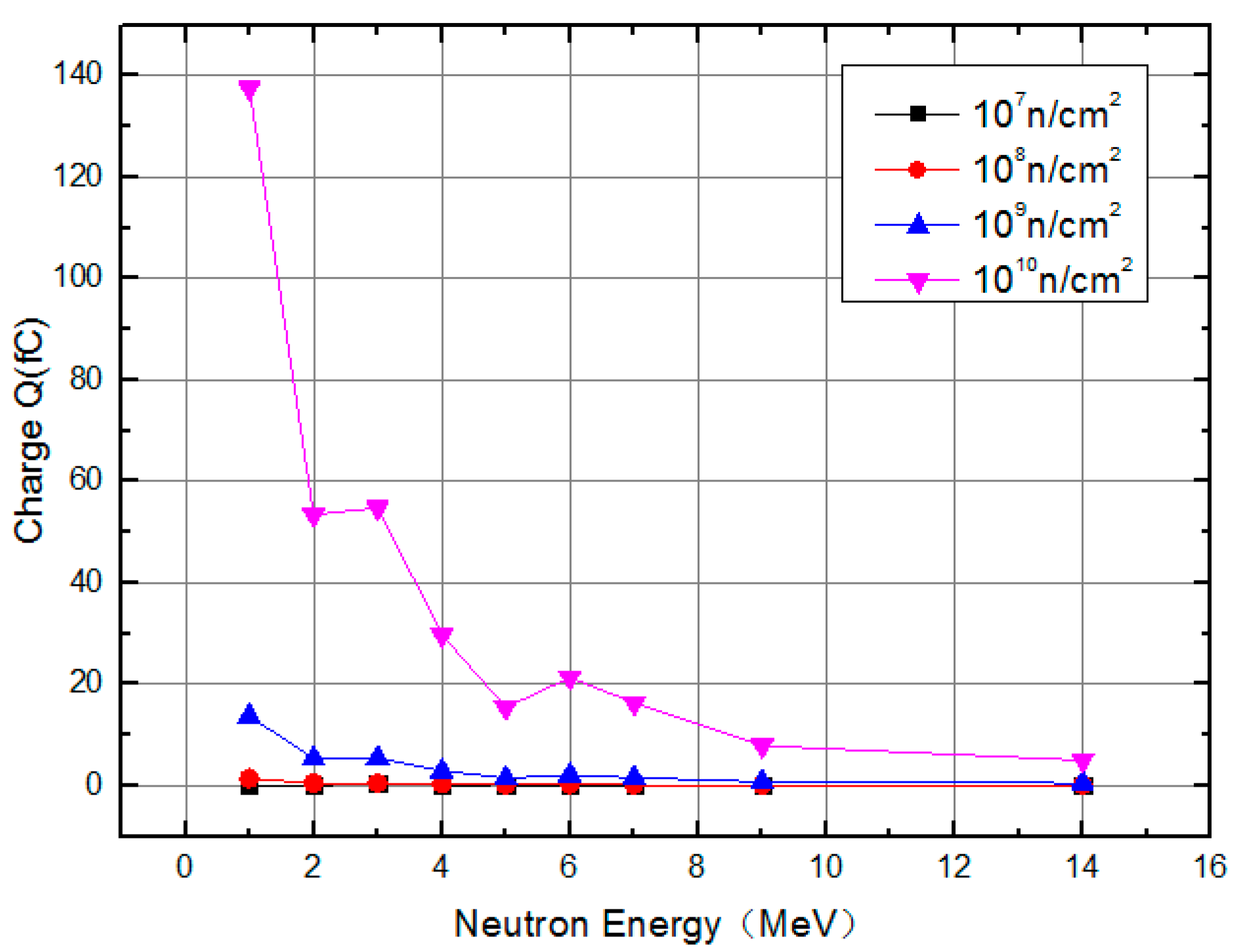
Based on Geant4’s neutron-ionizing-energy-deposition data and Formula (1), it can be known that when the neutron fluence is one, the collected charge generated by 1 MeV neutrons in 1 μm3 of sensitive area is approximately 4.34 × 10⁻¹⁰ fC, which is far less than the critical charge (about 2 fC) of a 0.13 μm device node turnover. Therefore, a single neutron will not cause localized latch-up in the microprocessor. This is also mutually verified by the experimental result that the microprocessor does not experience functional interruption under low neutron-flux irradiation conditions. It is assumed that all ionized charges are collected, and the calculation results of the charge collected in the sensitive zone of the transistor under different reactor neutron injection quantity are shown in Figure 6. When the neutron injection quantity is 107~108 n/cm2, the collected charge in the sensitive zone is less than 1 fC. When the neutron fluence is 109 n/cm2, the collected charge in the sensitive zone exceeds the critical charge (about 2 fC). Since integrated circuits are essentially formed by stacking a large number of CMOS devices according to specific rules, it can be inferred from the above that the variations in node voltage and internal electric potential of CMOS devices under high-flux neutron irradiation are caused by the synergistic effect of multiple neutron secondary ionizations, which in turn induces local latch-up in the microprocessor.

3.3. Analysis of Radiation Effect Mechanism

Neutrons are electrically neutral particles, which do not ionize directly when reacting with materials, but indirectly ionize through the following forms: (1) neutron collides with nucleons to reach an excited state, and then deexcite to release gamma rays; (2) neutrons eject recoil atoms or ions from the lattice; (3) the participation of neutrons in nuclear reactions may release charged particles, such as the ionization of alpha particles and protons in (n, α) and (n, p) reactions; (4) neutrons interact with trace natural elements uranium and thorium in the microprocessor packaging material to generate fission reactions, resulting in fission fragments. Secondary charged particles produced by the above forms of ionization will generate ionizing-energy-deposition near their tracks during transport within the transistor, exciting electron–hole pairs, which are collected by the sensitive region of the transistor (depletion layer).
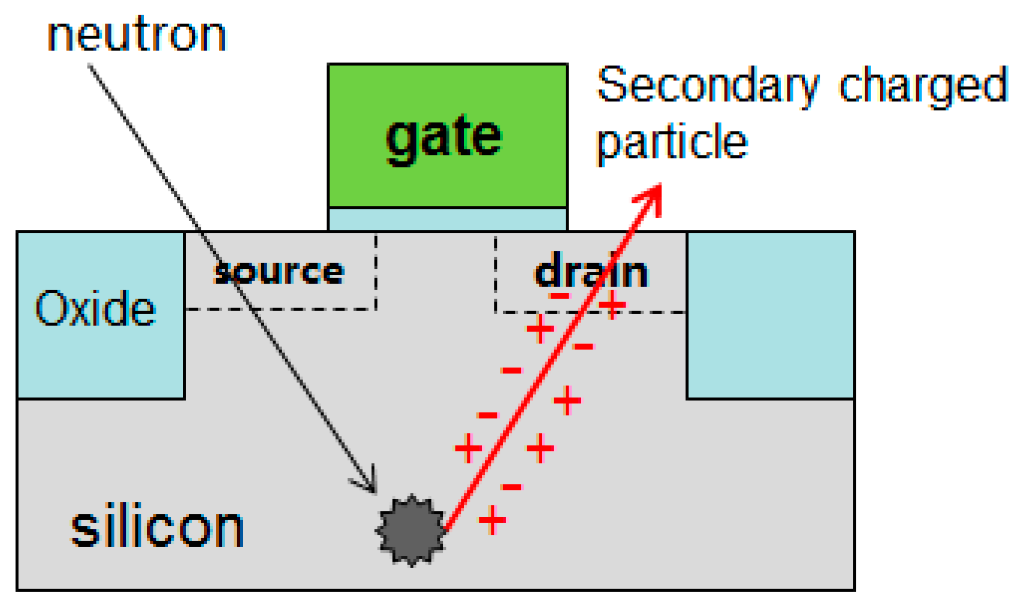
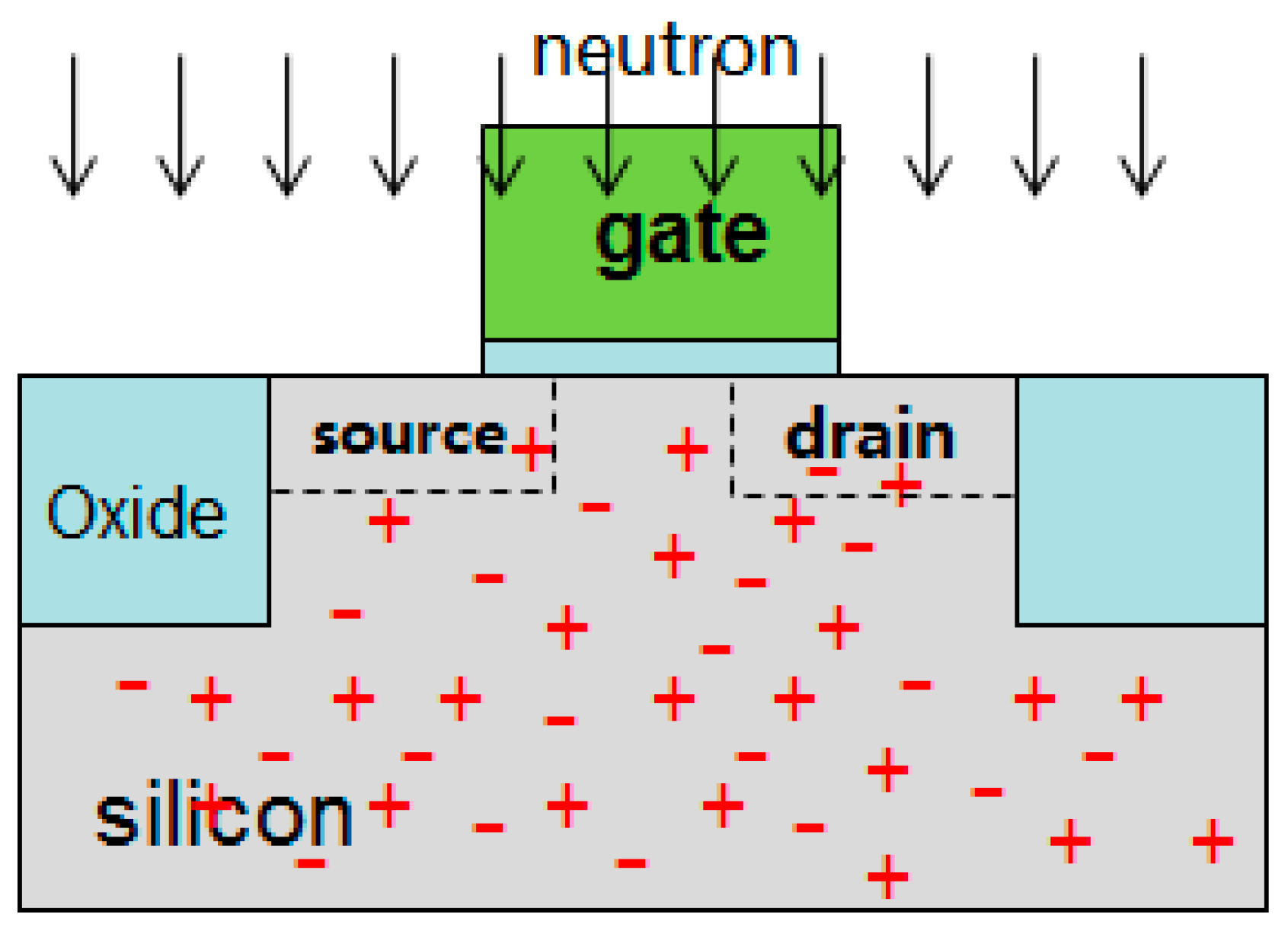
Although the physical process of neutron and material reaction is the same, the charge spatial distribution, collection mechanism and influencing factors of single neutron incident and high-flux neutron-incident semiconductor devices are quite different. Figure 7 is a schematic diagram of the typical single-particle effect of neutrons. Its charge is mainly generated on the track of secondary charged particles generated by the reaction of neutrons with silicon materials, and the generation and collection of charge are related to particle incidence Angle. Figure 8 shows the schematic diagram of secondary ionization effect of a high-flux neutron-incident semiconductor device. Due to the high flux, the secondary ionization charge of neutrons can be regarded as approximately evenly distributed in the PN junction and oxide layer of the entire device (independent of the neutron-incident Angle), and is collected under the action of applied electric field to form transient current, which causes circuit turnover and locking, data loss and function interruption. In addition, since the anti-ionizing radiation dose of the test circuit can reach 1000 Gy(Si), and the total concomitant gamma radiation dose of the reactor is about tens of Gy(Si) under the neutron-irradiation fluence of 1.6 × 10¹³ n/cm2, the influence of the total radiation dose effect is ignored.
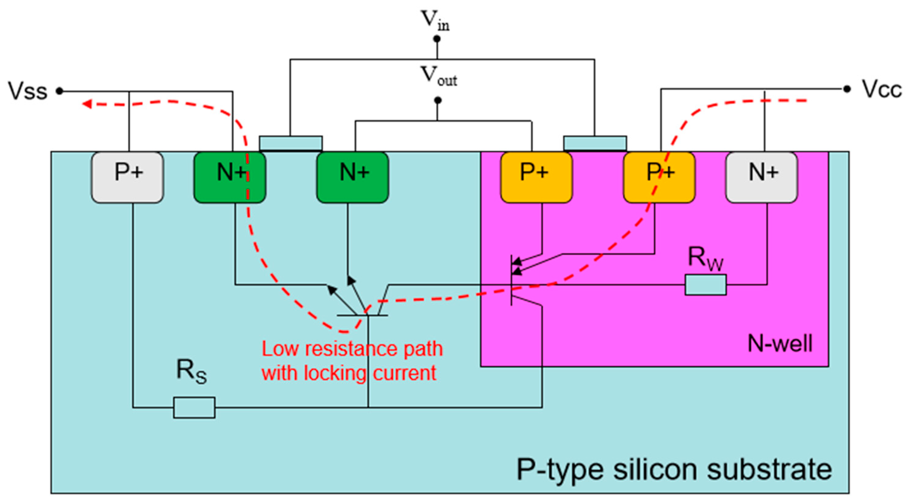
According to the characteristics of a working current jump, function interruption and recovery after power failure and restart of the test circuit, it can be judged that the charge collection reaches a certain threshold to trigger the conduction of the parasitic structure of PNPN inside the microprocessor, and thus the locking effect occurs. Because the current hop is smaller than the current in the transient dose rate locking effect [22], and only the square-wave signal is interrupted in the microprocessor while the reference voltage output remains normal, it can be determined that part of the functional modules (CPU, SRAM, etc.) in the microprocessor circuit only associated with the square-wave signal output have locking, that is, a micro latch-up effect.
As shown in Figure 9, the four-layer parasitic circuit model consists of parasitic npn and pnp transistors as well as substrate resistance and well resistance. The SCR structure is usually closed. Under radiation conditions, due to ionizing-energy-deposition generated by the charge under the action of an external electric field to form a current, any transistor base-emitter voltage drop rise, such as the n-well resistance Rw voltage being greater than the parasitic npn transistor base-emitter positive voltage drop, will cause npn transistor conduction and produce current flowing through the Rs resistance. If the Rs voltage is greater than the positive voltage drop of the parasitic PNP transistor base-emitter, it will cause the PNP transistor to switch on, which in turn will increase the current flowing through the Rw. Once the gain product of the two transistors is greater than 1 (βnpn × βpnp > 1), the current cycle increases until both transistors reach saturation. At this time, the larger current in the circuit has changed the effective doping conditions in the silicon material, and the entire path becomes low impedance. Although reactor neutrons have relatively low energy and the single-particle turnover cross-section is extremely small, the critical charge of deep-submicron devices is also very small. Consequently, under conditions of high neutron flux, the collected charge from multiple nodes can easily reach or exceed the critical charge required for upset, leading to errors in multiple bits or even a large number of cells. Furthermore, as the neutron flux increases further, latch-up effects become inevitable.

4. Conclusions

In this paper, 130 nm bulk silicon CMOS integrated circuit is taken as the object to study the neutron-radiation effect of deep submicron integrated circuit under the irradiation of reactor high flux. Through experiments and simulation calculations, it is found that the deep submicron CMOS circuit is very sensitive to lower-energy neutron ionizing radiation of the reactor. The main physical mechanism is that the collected charge caused by the secondary ionization of high-flux neutrons in the device forms transient surge current, resulting in a large number of unit turnover and even locking. That would be a more serious problem for new electronic equipment that works in a reactor environment.

Author Contributions

Conceptualization, M.L., C.Z., G.X., X.X., L.Z. and C.D.; methodology, M.L., C.Z., G.X., Y.W., X.X., L.Z., D.Y., Y.Z. and C.D.; software, M.L., C.Z., G.X., Y.W. and L.Z.; validation, M.L., C.Z., G.X., X.X. and C.D.; formal analysis, C.Z. and Y.W.; investigation, M.L., C.Z., G.X., Y.W., X.X., L.Z. and C.D.; data curation, M.L. and G.X.; writing—original draft preparation, M.L. and L.Z.; writing—review and editing, C.D.; supervision, C.D. All authors have read and agreed to the published version of the manuscript.

Funding

This research was funded by National Natural Science Foundation of China, grant number 12305313; Innovation Foundation of Radiation Resistance Application Technology Innovation Center, grant number KFZC2025021301; Basic Research Project of National Key Laboratory of Neutron Science and Technology, grant number NST20250308.

Data Availability Statement

The original contributions presented in this study are included in the article. Further inquiries can be directed to the corresponding authors.

Conflicts of Interest

The funders had no role in the design of the study; in the collection, analyses, or interpretation of data; in the writing of the manuscript; or in the decision to publish the results. The authors declare no conflicts of interest.

Abbreviations

The following abbreviations are used in this manuscript:
SEEsingle-event effects
SELsingle-event latch-up
SETsingle-event transient
SEUsingle-event upset
IELionizing-energy loss
NIELnon-ionizing-energy loss
PKAPrimary Knock-on Atom
SKASecondary Knock-on Atom

References

  1. Gossett, C.A.; Hughlock, B.W.; Katoozi, M.; LaRue, G.S.; Wender, S.A. Single event phenomena in atmospheric neutron environments. IEEE Trans. Nucl. Sci. 1993, 40, 1845–1852. [Google Scholar] [CrossRef]
  2. Jin, X.; Yuanming, W.; Shanchao, Y.; Qiang, M.; Yan, L.; Dongsheng, L.; Wei, C. Geant4 application in neutron radiation effects. At. Energy Sci. Technol. 2012, 46, 607–610. [Google Scholar]
  3. Dyer, C.S.; Clucas, S.N.; Sanderson, C.; Frydland, A.D.; Green, R.T. An experimental study of single-event effects induced in commercial SRAMs by neutrons and protons from thermal energies to 500 MeV. IEEE Trans. Nucl. Sci. 2004, 51, 2817–2824. [Google Scholar] [CrossRef] [Scilit]
  4. Olsen, J.; Becher, P.E.; Fynbo, P.B.; Raaby, P.; Schultz, J. Neutron-Induced Single Event Upsets In Static Rams Observed At 10-Km Flight Altitude. IEEE Trans. Nucl. Sci. 1993, 40, 74–77. [Google Scholar] [CrossRef] [Scilit]
  5. Chadwick, M.B.; Normand, E. Use of new ENDF/B-VI proton and neutron cross sections for single event upset calculations. IEEE Trans. Nucl. Sci. 1999, 46, 1386–1394. [Google Scholar] [CrossRef] [Scilit]
  6. Normand, E.; Oberg, D.L.; Wert, J.L.; Ness, J.D.; Majewski, P.P.; Wender, S. Single event upset and charge collection measurements using high energy protons and neutrons. IEEE Trans. Nucl. Sci. 1994, 41, 2203–2209. [Google Scholar] [CrossRef] [Scilit]
  7. Dyer, C.; Hands, A.; Ford, K.; Frydland, A.; Truscott, P. Neutron-Induced Single Event Effects Testing Across a Wide Range of Energies and Facilities and Implications for Standards. IEEE Trans. Nucl. Sci. 2006, 53, 3596–3601. [Google Scholar] [CrossRef] [Scilit]
  8. Clemens, M.A.; Sierawski, B.D.; Warren, K.M.; Mendenhall, M.H.; Dodds, N.A.; Weller, R.A.; Baumann, R.C. The Effects of Neutron Energy and High-Z Materials on Single Event Upsets and Multiple Cell Upsets. IEEE Trans. Nucl. Sci. 2011, 58, 2591–2598. [Google Scholar] [CrossRef] [Scilit]
  9. Baggio, J.; Lambert, D.; Ferlet-Cavrois, V.; Paillet, P.; Marcandella, C.; Duhamel, O. Single Event Upsets Induced by 1–10 MeV Neutrons in Static-RAMs Using Mono-Energetic Neutron Sources. IEEE Trans. Nucl. Sci. 2007, 54, 2149–2155. [Google Scholar] [CrossRef] [Scilit]
  10. Pereira, E.C.F.; Gonçalez, O.L.; Vaz, R.G.; Federico, C.A.; Both, T.H.; Wirth, G.I. The effects of total ionizing dose on the neutron SEU cross section of a 130 nm 4 mb SRAM memory. In 2014 15th Latin American Test Workshop–LATW; IEEE: Piscataway, NJ, USA, 2014; pp. 1–4. [Google Scholar] [CrossRef] [Scilit]
  11. Hands, A.; Morris, P.; Dyer, C.; Ryden, K.; Truscott, P. Single Event Effects in Power MOSFETs and SRAMs Due to 3 MeV, 14 MeV and Fission Neutrons. IEEE Trans. Nucl. Sci. 2011, 58, 952–959. [Google Scholar] [CrossRef] [Scilit]
  12. Lambert, D.; Desnoyers, F.; Thouvenot, D.; Riant, O.; Galinat, J.; Azaïs, B.; Colladant, T. Single event upsets induced by a few MeV neutrons in SRAMs and FPGAs. In 2017 IEEE Radiation Effects Data Workshop (REDW); IEEE: Piscataway, NJ, USA, 2017; pp. 1–5. [Google Scholar] [CrossRef] [Scilit]
  13. Irom, F.; Miyahira, T.F.; Nguyen, D.N.; Jun, I.; Normand, E. Results of recent 14 MeV neutron single event effects measurements conducted by the jet propulsion laboratory. In 2007 IEEE Radiation Effects Data Workshop; IEEE: Piscataway, NJ, USA, 2007; pp. 141–145. [Google Scholar] [CrossRef] [Scilit]
  14. Guo, X.; Guo, H.X.; Wang, G.Z.; Lin, D.S.; Chen, W.; Bai, X.Y.; Liu, Y. Simulations of single-event upset in SRAMs induced by neutrons with Geant4. At. Energy Sci. Technol. 2010, 44, 362–367. [Google Scholar]
  15. Normand, E.; Wert, J.L.; Majewski, P.P.; Oberg, D.L.; Bartholet, W.G.; Davis, S.K.; Gavron, A. Single event upset and latchup measurements in avionics devices using the WNR neutron beam and a new neutron-induced latchup model. In Proceedings of 1995 IEEE Nuclear and Space Radiation Effects Conference (NSREC’95); IEEE: Piscataway, NJ, USA, 1995; pp. 33–38. [Google Scholar] [CrossRef] [Scilit]
  16. Schwank, J.R.; Shaneyfelt, M.R.; Baggio, J.; Dodd, P.E.; Felix, J.A.; Ferlet-Cavrois, V.; Blackmore, E. Effects of Angle of Incidence on Proton and Neutron-Induced Single-Event Latchup. IEEE Trans. Nucl. Sci. 2006, 53, 3122–3131. [Google Scholar] [CrossRef]
  17. Tausch, J.; Sleeter, D.; Radaelli, D.; Puchner, H. Neutron induced micro SEL events in COTS SRAM devices. In 2007 IEEE Radiation Effects Data Workshop; IEEE: Piscataway, NJ, USA, 2007; pp. 185–188. [Google Scholar] [CrossRef] [Scilit]
  18. Merelle, T.; Saigné, F.; Sagnes, B.; Gasiot, G.; Roche, P.; Carriere, T.; Palau, J.M. Monte-Carlo simulations to quantify neutron-induced multiple bit upsets in advanced SRAMs. IEEE Trans. Nucl. Sci. 2005, 52, 1538–1544. [Google Scholar] [CrossRef] [Scilit]
  19. Wrobel, F.; Palau, J.M.; Calvet, M.C.; Bersillon, O.; Duarte, H. Simulation of nucleon-induced nuclear reactions in a simplified SRAM structure: Scaling effects on SEU and MBU cross sections. IEEE Trans. Nucl. Sci. 2001, 48, 1946–1952. [Google Scholar] [CrossRef]
  20. Jin, X.; Palau, J.M.; Calvet, M.C.; Bersillon, O.; Duarte, H. Single event upset on static random access memory devices due to spallation, reactor, and monoenergetic neutrons. Chin. Phys. B 2019, 28, 1–10. [Google Scholar] [CrossRef] [Scilit]
  21. Wittmann, R.; Selberherr, S. A study of ion implantation into crystalline germanium. Solid-State Electron. 2007, 51, 982–988. [Google Scholar] [CrossRef] [Scilit]
  22. Du, C.; Zhao, H.; Deng, Y. Latent Damage in 0.13 μm Large Scale Integrated Circuit from Transient Latchup Test. Yuanzineng Kexue Jishu 2019, 53, 2498–2503. [Google Scholar]
Figure 1. The reactor neutron spectrum.
Electronics 15 04585 g001
Figure 2. Test circuit of 130 nm CMOS bulk Si microprocessor.
Electronics 15 04585 g002
Figure 3. Simplified model of 130 nm transistor.
Electronics 15 04585 g003
Figure 4. Power supply current at different neutron fluence.
Electronics 15 04585 g004
Figure 5. IEL/NIEL energy-deposition ratio of 1–14 MeV neutrons in a sensitive region of 1 μm3.
Electronics 15 04585 g005
Figure 6. Charge collection in the sensitive region of transistor at different neutron fluence.
Electronics 15 04585 g006
Figure 7. Neutron single-event effect.
Electronics 15 04585 g007
Figure 8. Neutron-induced ionizing effect at high neutron flux.
Electronics 15 04585 g008
Figure 9. The latch-up structure and low-resistor path of CMOS.
Electronics 15 04585 g009
Table 1. Neutron-irradiation experiment results.
Experiment CircuitNeutron-Flux
n·cm−2·S−1
Neutron Fluence
n/cm2
Number of
Current Jumps
Experimental Phenomenon
#14 × 1091.6 × 101345The working current jumps and is accompanied by function interruption. The 1.2 V level signal is normal.
#24.4 × 1091.6 × 101349
Disclaimer/Publisher’s Note: The statements, opinions and data contained in all publications are solely those of the individual author(s) and contributor(s) and not of MDPI and/or the editor(s). MDPI and/or the editor(s) disclaim responsibility for any injury to people or property resulting from any ideas, methods, instructions or products referred to in the content.