Article

An 8-Bit Four-Channel Time-Interleaved SAR-Flash Hybrid ADC with Time-Domain Interpolation

1
Department of Electronic Engineering, Faculty of Applied Energy System, Jeju National University, Jeju 63543, Republic of Korea
2
Department of Electronics Engineering, Chungnam National University, Daejeon 34134, Republic of Korea
*
Authors to whom correspondence should be addressed.
Electronics 2026, 15(18), 4232; https://doi.org/10.3390/electronics15184232
Submission received: 3 August 2026 / Revised: 5 September 2026 / Accepted: 16 September 2026 / Published: 17 September 2026
(This article belongs to the Section Circuit and Signal Processing)

Abstract

An 8-bit 3.2 GS/s four-channel time-interleaved (TI) successive-approximation-register (SAR)-flash analog-to-digital converter (ADC) employing complementary dynamic amplifier (CDA)-based two-step sub-ADCs is presented for high-speed wired and wireless communication systems. Each sub-ADC uses four CDAs to perform a 4-bit asynchronous loop-unrolled (LU) SAR conversion followed by a 4.5-bit reference-embedded interpolating flash (I-Flash) conversion, achieving 8-bit resolution with reduced comparator count and input capacitance. A four-channel TI architecture with a multi-phase clock generator and an on-chip voltage-controlled delay line (VCDL) enables 3.2 GS/s operation while performing foreground offset calibration under full TI loading to accurately track inter-channel reference variations. Fabricated in a 28 nm CMOS process, the prototype ADC shows differential non-linearity (DNL) and integral non-linearity (INL) ranges of −0.78 to +0.74 LSB and −0.84 to +1.03 LSB, respectively, and achieves a signal-to-noise and distortion ratio (SNDR) and a spurious-free dynamic range (SFDR) of 41.74 dB and 58.03 dB at 3.2 GS/s with a Nyquist-rate input. Operating from a 1 V supply, the ADC core consumes 8.63 mW at 3.2 GS/s, corresponding to a Walden figure-of-merit (FoM) of approximately 27 fJ/conversion step.

1. Introduction

In high-speed wired and wireless communication systems, as well as in applications requiring large-volume data transfer, analog-to-digital converters (ADCs) capable of multi-GS/s sampling rates and medium-to-high resolution have become indispensable. The widespread adoption of multi-level modulation schemes such as PAM-4 and PAM-8 further increases the demand for high-speed and high-accuracy data conversion at both the transmitter and receiver, continuously driving the need for high-speed ADCs [1,2,3,4,5,6]. To meet these requirements, time-interleaved (TI) architectures, in which multiple sub-ADCs operate in parallel to scale the overall sampling rate in proportion to the number of channels, have been widely adopted, making TI ADCs a key solution for high-speed systems [7,8,9,10,11,12,13,14]. However, adopting the TI architecture does not simply increase the conversion speed.
Channel mismatches including offset, gain, timing skew, and bandwidth variation are inevitable in TI systems [15,16,17], and the circuits and digital algorithms required to suppress these errors significantly increase power consumption and architectural complexity. In particular, in high-speed and high-resolution TI ADCs, calibration-related circuits often occupy a substantial portion of the total power budget [18,19,20,21], posing a critical limitation to power efficiency and system-level integration. Therefore, designing an efficient high-speed TI ADC requires not only increasing the interleaving factor but also employing power-efficient sub-ADCs and choosing an appropriate number of channels to alleviate calibration and clock-distribution burdens. From this perspective, this work adopts a previously reported complementary dynamic amplifier (CDA)-based low-power sub-ADC architecture [22] to achieve improved power and area efficiency in TI operation. With a dual-edge operating scheme, a CDA-based sub-ADC can realize 8-bit resolution using only four CDAs, offering significant energy and area advantages over conventional medium-resolution high-speed ADCs. By employing this CDA-based low-power sub-ADC as the fundamental building block of the TI architecture, the proposed design achieves the target sampling rate without relying on excessively high interleaving factors while simultaneously reducing the calibration and clock-distribution burdens. This work implements a four-channel TI ADC using a CDA-based two-step sub-ADC, achieving an overall sampling rate of 3.2 GS/s. Each sub-ADC operates at a relatively low clock frequency, ensuring sufficient timing margin, while the TI architecture collectively provides the required high-speed sampling. Furthermore, clock generation optimized for channel-to-channel matching, together with offset calibration performed under realistic TI operating conditions, validates the suitability of the proposed architecture for high-speed and low-power TI ADCs. Accordingly, the main contribution of this work lies in the practical extension of a previously demonstrated single-channel CDA-based ADC to a four-channel TI implementation, rather than in proposing a fundamentally new ADC architecture. The work addresses the additional design challenges that arise from multi-channel implementation and provides the associated circuit-level design considerations and verification results. The remainder of this paper is organized as follows. Section 2 describes the overall TI ADC architecture and the CDA-based sub-ADC. Section 3 presents the circuit implementation in the TI environment, and Section 4 discusses the measurement results, followed by conclusions.

2. Proposed TI ADC Architecture

2.1. Overall Architecture of the Four-Channel TI ADC

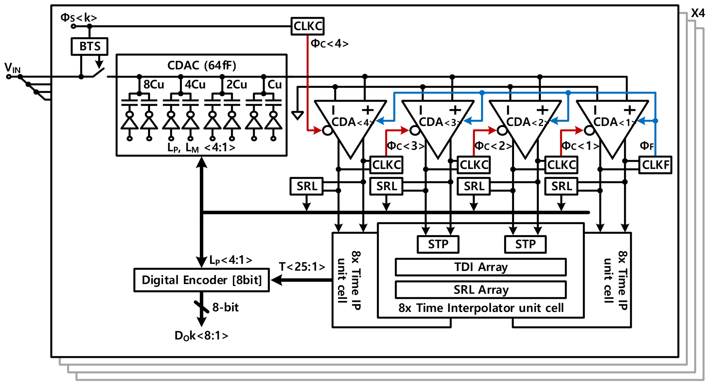
In the proposed ADC, each sub-ADC employs a CDA-based two-step architecture and operates reliably under low-power conditions. Four identical sub-ADCs are driven in a time-interleaved manner using evenly spaced sampling clock phases, resulting in an overall sampling rate of 3.2 GS/s. Since each sub-ADC operates at a relatively low internal clock frequency, the proposed architecture effectively mitigates comparator delay, capacitive digital-to-analog converter (CDAC) settling requirements, and high-frequency clocking demands that would arise if a single ADC were directly operated at multi-GS/s rates. The TI configuration thus preserves the simplicity and power efficiency of the sub-ADCs while multiplying the overall conversion rate, and a block diagram of the proposed system is shown in Figure 1. An external differential clock is first converted into an internal pulse signal by a low-voltage differential signaling (LVDS) receiver, and then four sampling clock phases are generated by a multi-phase clock generator, followed by a voltage-controlled delay line (VCDL)-based architecture that provides fine time-skew correction between channels with high resolution under the same area constraint. Using these generated sampling clocks (Φ1:4), each sub-ADC independently performs coarse-fine conversion. The conversion results from the four channels are then multiplexed sequentially, forming a continuous output data stream. The proposed TI scheme achieves a high overall sampling rate while minimizing the clock frequency and circuit burden of each sub-ADC. In particular, it alleviates CDAC switching stress, comparator delay, and clock-distribution burden, enabling robust high-speed operation.

2.2. Sub-ADC Overview

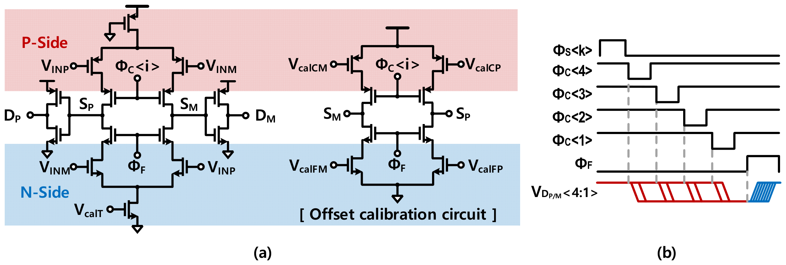
Figure 2 shows the block diagram of the proposed TI sub-ADC. It is composed of four CDAs and performs an 8-bit conversion. The MSB is resolved sequentially using a loop-unrolled (LU) successive approximation register (SAR) operation, while the lower bits are obtained through a fast-interpolating flash (I-Flash) conversion. Each CDA incorporates both PMOS and NMOS input pairs and operates as a dual-edge amplifier by selecting the charging and discharging paths at the rising and falling clock edges, respectively. This enables the realization of 8-bit resolution (4-bit LU-SAR + 4.5-bit I-Flash) using only four CDAs. During the sampling phase, the input signal is stored on the top plate of the CDAC through dedicated bootstrapped switches (BTS), while the CDAC control nodes are held at their initial reference levels. Figure 3a illustrates the schematic of the CDA with the foreground offset-calibration circuitry based on the offset-calibration approach in [23], while Figure 3b shows the timing diagram of the asynchronous clocks and the waveform at the CDA output node VDP/M. In this offset-calibration scheme, the effective offset of the coarse ADC is adjusted by tuning auxiliary PMOS current sources, whereas the offset of the fine ADC is compensated by using NMOS-based auxiliary current sources and tail-current control. After sampling, when the ΦC<4> clock transitions low, the P-side of CDA<4> is activated to initiate the comparison. The MSB is then determined and latched by the SR-latch (SRL) according to the discharge-rate difference between the CDA output nodes. All CDA clocks, including CLKC and CLKF, are generated by the asynchronous logic. After the MSB capacitor of the CDAC is switched, the P-side of the next CDA is sequentially activated in accordance with the CDAC settling time. In this manner, the upper four bits are resolved in a conventional LU-SAR sequence, starting from CDA<4> and ending with CDA<1>. To prevent shoot-through current in the PIs during the LU-SAR operation, shoot-through-prevention (STP) blocks are inserted between the CDAs and PIs. The STP blocks disable signal transfer to the PIs during the LU-SAR operation and enable the signal path only during the I-Flash operation.
Once the LU-SAR conversion is completed, the CDA outputs are reset to the reference level through a complementary path using the NMOS input pairs, and the same four CDAs used in the coarse stage are reused for the I-Flash conversion. In the I-Flash conversion, the N-sides of the four CDAs are activated simultaneously, generating 25 zero-crossings through a reference-embedded 8× interpolation architecture. The time-domain interpolator (TDI) array receives the timing information generated by adjacent CDA outputs and produces additional intermediate timing points between them, thereby realizing the 8× interpolation without requiring additional CDAs. The interpolated timing signals are then applied to the SRL array, where the relative arrival order of the interpolated signals is sensed and latched. Accordingly, each SRL provides a digital decision corresponding to an interpolated zero-crossing point, and the resulting 25 decisions form T<25:1>, which is subsequently processed by the digital encoder to determine the lower-bit output. This provides sufficient resolution for determining the lower 4.5 bits and reduces the total number of required conversions for an 8-bit decision from eight conversions to approximately five. By combining the LU-SAR and reference-embedded I-Flash operations, the sub-ADC achieves full 8-bit conversion with a compact area and low power consumption.

3. Circuit Implementation

3.1. Multi-Phase Clock Generation

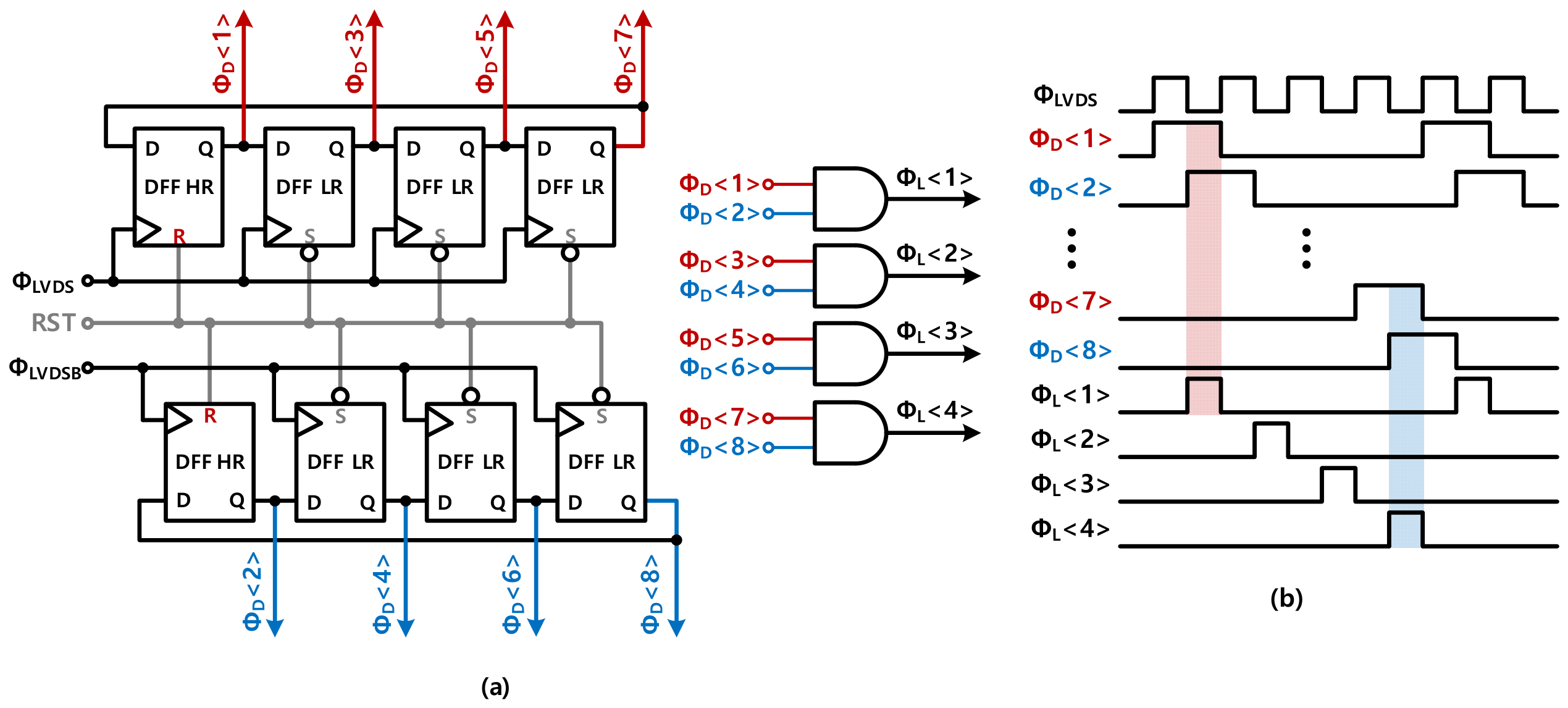
Figure 4 illustrates the block diagram of the proposed multi-phase clock generator and its associated timing diagram. Non-overlapping sampling clocks are required to prevent simultaneous sampling between adjacent TI channels and to ensure stable channel-to-channel sampling operation in the presence of clock skew and delay variations. Without any additional logic, generating non-overlapping clocks using only a single ring counter requires an input clock running at twice the target sampling frequency, which significantly increases the design burden. To avoid this, the architecture shown in Figure 4a is adopted to generate multi-phase clocks from an input clock operating at the desired sampling frequency. The proposed multi-phase clock generator consists of two ring counters, each composed of three set-mode D Flip Flops (DFFs) and one reset-mode DFF, and four AND gates. ΦLVDS and ΦLVDSB drive each ring counter, and four-phase clocks with a 25% duty cycle are generated on the rising edge of ΦLVDS. Similarly, another set of four 25% duty clocks is generated on the falling edge of ΦLVDS. Thus, after generating a total of eight 25% duty clocks, the clocks derived from the rising and falling edges are combined through AND gates to finally produce four non-overlapping clocks. This operation is illustrated in the timing diagram shown in Figure 4b. The timing stability of the generated sampling clocks was also verified through transient-noise simulations. With a noise bandwidth of up to 100 GHz, the RMS jitter of the four sampling clocks, evaluated over 1000 samples, ranges from approximately 92.9 fs to 97.5 fs. At an input frequency of 1.599 GHz, these values correspond to a jitter-limited SNR of approximately 60.2–60.6 dB, or an equivalent resolution of approximately 9.7 bits. Since this resolution is higher than the nominal 8-bit resolution of the proposed ADC, the contribution of sampling-clock jitter to the measured ADC performance is negligible.
Although the random jitter of the generated clocks is sufficiently small, the four sampling clocks (ΦL<1:4>) for the proposed four-channel TI SAR ADC inherently exhibit phase deviations caused by device variation and routing asymmetry. These phase differences translate directly into sampling-time skew among the channels, which becomes increasingly critical at multi-GS/s operation.
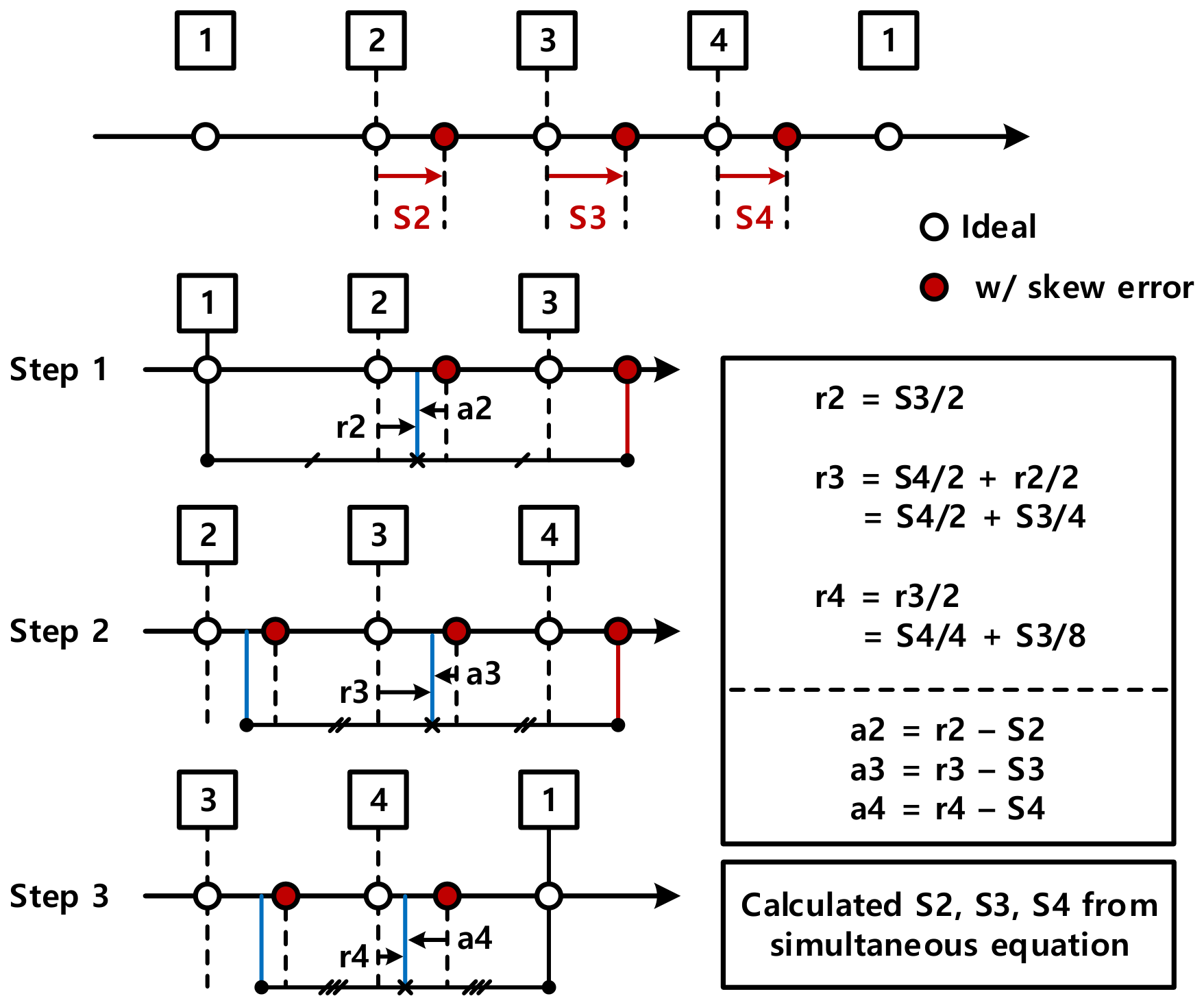
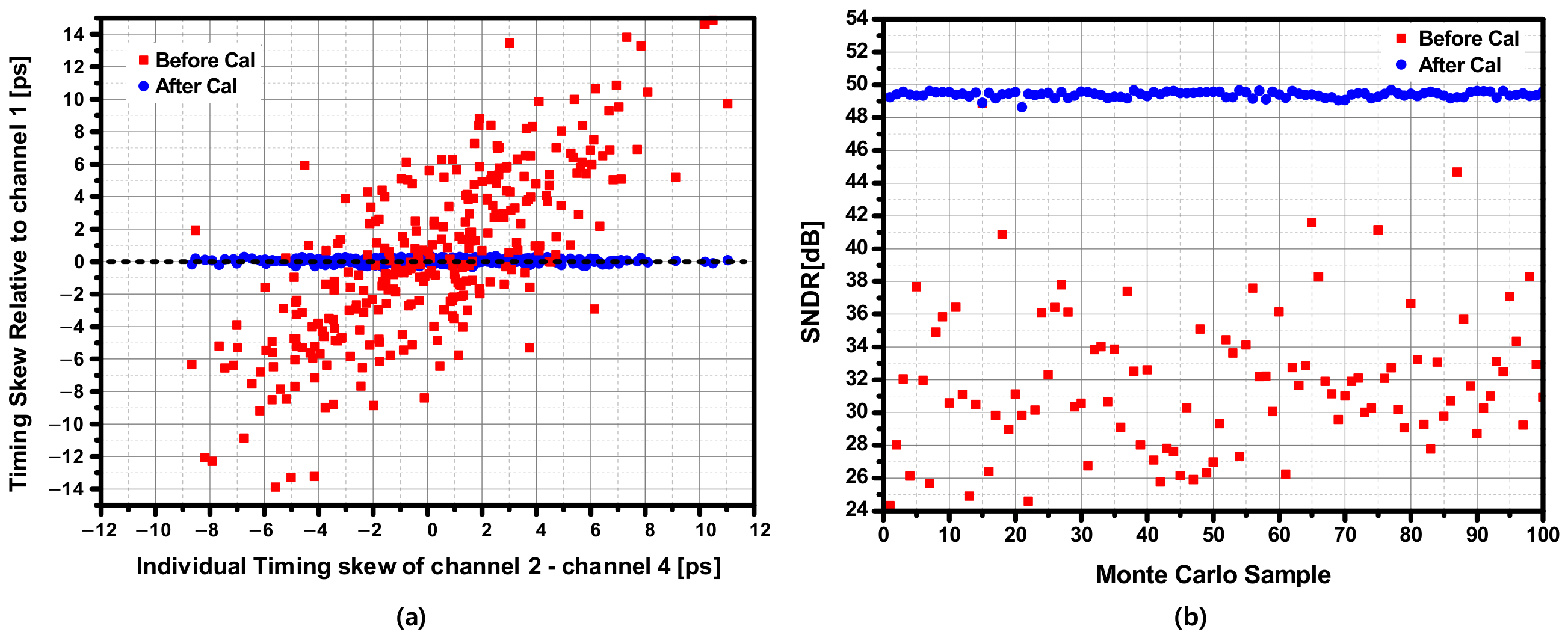
To mitigate this issue, the proposed design employs an on-chip VCDL-based phase-alignment scheme to finely adjust the sampling phase of each channel. Figure 5 illustrates the overall digital timing-skew detection and correction procedure. During post-silicon characterization, a single-tone sinusoidal signal is applied to the ADC, and the digitized output sequences of the interleaved channels are processed to estimate the timing-skew error using the method described in [24]. To further verify the effectiveness of the timing-skew calibration engine applied in this work, Figure 6 presents MATLAB R2025b-based behavioral simulation results using a timing-skew distribution derived from circuit-level Monte Carlo simulations. The Monte Carlo simulation of the sampling-clock paths was performed with 100 samples, resulting in a 1σ timing-skew variation of approximately 3.75 ps. Based on this result, channel timing errors following the same statistical distribution were applied to the MATLAB model to evaluate the calibration performance. Figure 6a shows the timing-skew calibration results for channels 2–4, with channel 1 used as the reference channel. The x-axis represents the signed individual timing skew applied to channels 2–4, while the y-axis represents the corresponding timing skew relative to channel 1. Before calibration, the relative timing errors are distributed over approximately −14 to +14 ps. After calibration, the timing-skew errors converge to within approximately ±350 fs around channel 1. Figure 6b shows the SNDR before and after calibration for each of the 100 Monte Carlo samples. Although the SNDR before calibration varies considerably depending on the randomly generated channel timing skews, the calibrated results consistently maintain an SNDR higher than 48 dB. These results confirm that the timing-skew calibration engine applied to the ADC effectively reduces inter-channel timing mismatch and restores ADC performance under the timing-skew variations obtained from the circuit-level Monte Carlo simulations. In the current implementation, the polarity of the timing-skew error is continuously detected in real time in a background manner during normal ADC operation. The estimated timing-error polarity or error metric is then used to determine the update direction of the VCDL control code for each channel. This procedure is repeated until the sampling-time mismatch among the channels is sufficiently reduced.
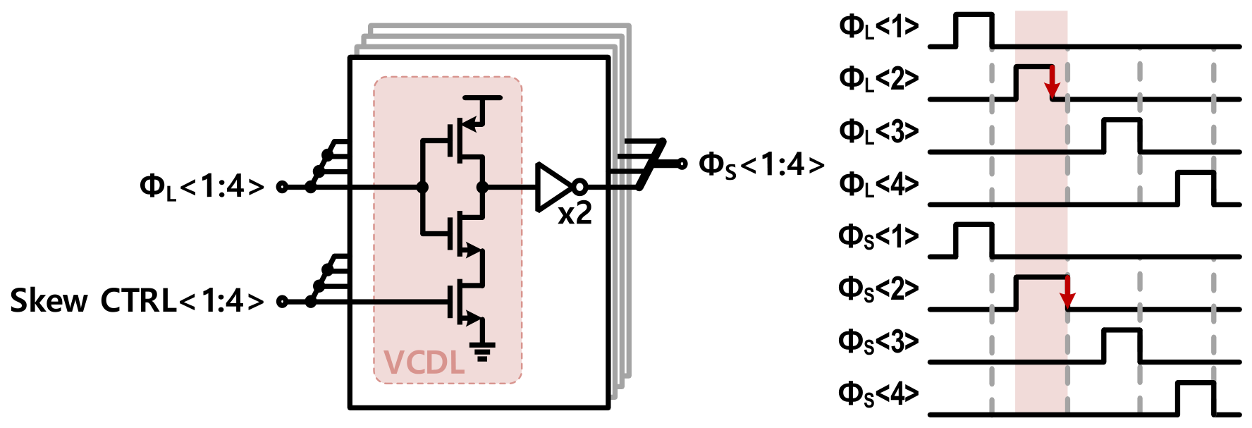
Figure 7 shows the detailed VCDL circuit and its corresponding timing diagram. Each VCDL receives one of the four uncorrected sampling clocks, ΦL<1:4>, and generates the corresponding phase-adjusted clock, ΦS<1:4>. When a channel is detected to sample earlier or later than the desired phase, its VCDL control code is updated to increase or decrease the delay in the compensating direction. Consequently, the sampling edges of ΦS<1:4> are more closely aligned, thereby reducing the sampling-phase mismatch among the four TI channels.

3.2. Offset Calibration and Gain Matching in TI

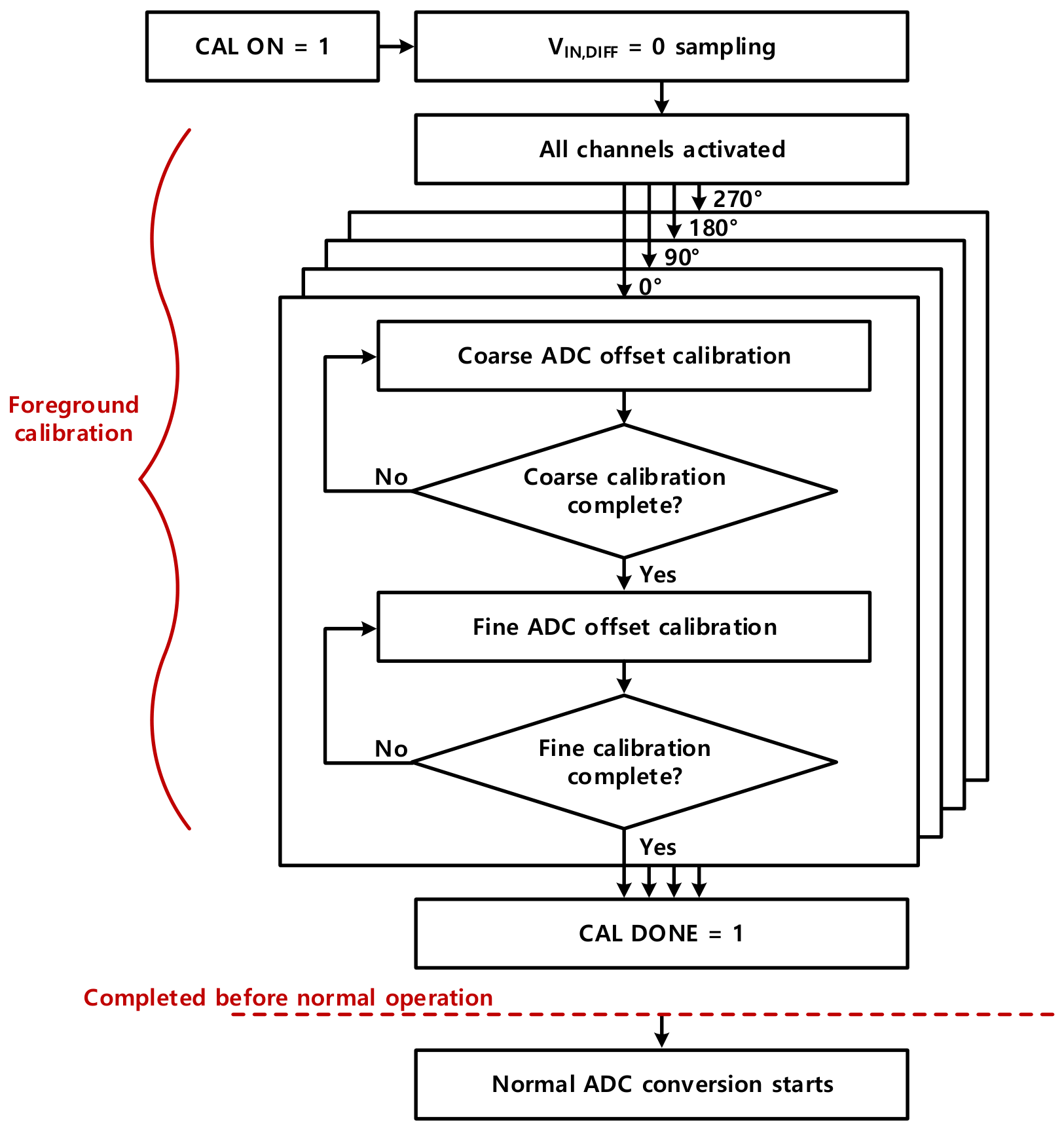
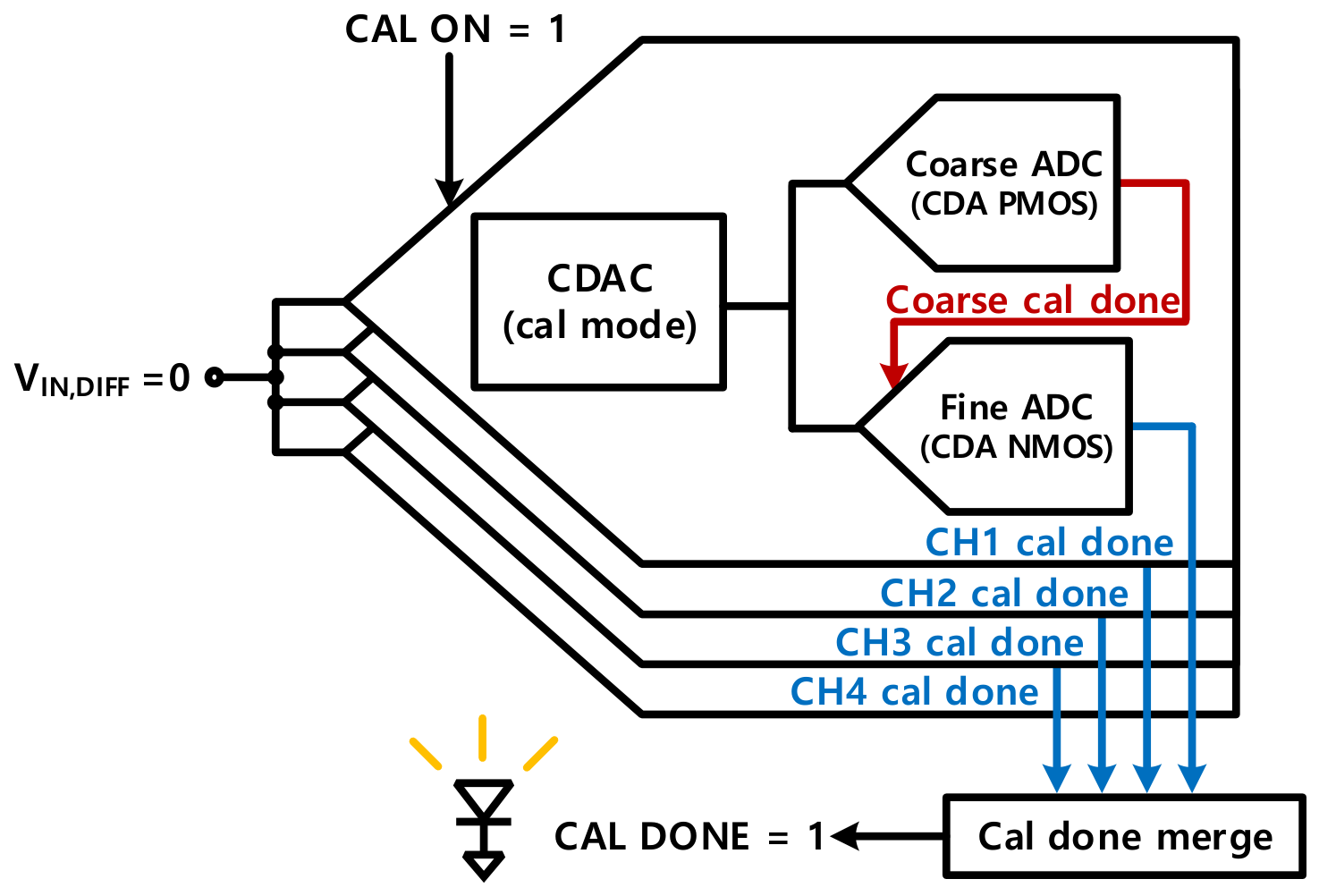
Figure 8 summarizes the foreground offset-calibration sequence, and Figure 9 illustrates the block-level implementation and control flow of the foreground calibration scheme. When the foreground calibration is initiated by asserting CAL ON, the input is sampled at V I N , D I F F = 0 , and the required offset voltages are sequentially generated by the CDAC in the calibration mode. First, the offset of the coarse ADC is calibrated by tuning the additional PMOS current sources to adjust the effective offset. Once the coarse offset calibration is completed, the coarse calibration completion flag signal is asserted, which triggers the fine ADC offset calibration. The fine ADC is then calibrated in a similar manner, using the offset voltages generated by the CDAC while adjusting NMOS-based auxiliary current sources and the tail current to compensate for its offset. After the fine calibration of each channel is completed, the channel-level calibration-done signals are merged to generate the final CAL DONE signal. As shown in Figure 8, the entire foreground calibration process is completed before normal ADC conversion starts.
In this way, the internal offset-calibration scheme of each sub-ADC can, in principle, be applied in the same manner as in a single-channel architecture. However, in a TI environment, multiple channels operate simultaneously, and accurate offset values are difficult to obtain unless the calibration is carried out under the same conditions as during normal operation. In particular, when the ADC is extended to a TI architecture, the overall circuit loading increases, and the CDAC reference-voltage distribution changes. Consequently, calibration performed with only a single active channel may not accurately reflect the actual TI operating conditions, resulting in offset errors. In other words, even slight differences in the CDAC reference levels experienced by individual channels may cause the offset values obtained through conventional calibration to deviate from those under actual TI operation. To address this issue, the foreground offset calibration is performed with all channels activated, while preserving the same operation sequence as in full TI operation. As shown in Figure 9, each channel performs coarse and fine offset calibration using the CDAC-generated calibration references, and the calibration-done signals from all channels are combined to determine the completion of the overall foreground calibration. That is, by calibrating the offset of each channel under the same loading conditions, reference-voltage variations, and switching activity as in TI operation, calibration errors caused by channel-to-channel reference deviations and operating-condition differences introduced by TI expansion can be reduced. Through this approach, more accurate offset values can be obtained under conditions that closely match the actual operating environment.
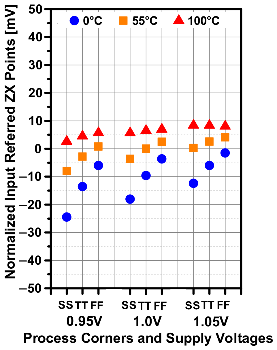
In addition, the calibration range was designed to sufficiently cover the offset variation caused by process, supply-voltage, and temperature variations. Figure 10 shows the simulated offset variation of CDA<4> under different PVT conditions. The calibration range was determined based on the worst-case PVT condition of SS, 0.95 V, and 0 °C and was designed to provide sufficient margin to cover the ±3σ offset variation under this condition. Therefore, the expected PVT-induced offset variation remains within the available calibration range.
Inter-channel gain mismatch was also considered in the four-channel TI implementation. Variations in the reference voltage supplied to each sub-ADC can result in gain differences among the channels. Therefore, the resistance of each reference-voltage path was designed such that the resulting channel-to-channel reference-voltage difference remains below 0.1 LSB based on the ADC input range. For the 8-bit ADC with a 0.8 V differential input range, 0.1 LSB corresponds to 0.3125 mV, or approximately 0.031% of the 1 V CDAC reference.

3.3. CDA Gain–Conversion Speed Trade-Off

In the adopted 8× time-domain interpolation architecture, the offset of each CDA and the 2× interpolated zero-crossing generated between adjacent CDAs are directly calibrated. The zero-crossing points generated by the subsequent 4× and 8× interpolation stages are not directly calibrated; instead, the effect of offsets introduced in these back-end interpolation stages is mitigated by providing sufficient time-domain gain in the front-end CDA. Therefore, sufficient CDA time-domain gain is important for maintaining the accuracy of the overall 8× time-domain interpolation. In this work, the differential input range is reduced from 1.2 V in [22] to 0.8 V, decreasing the LSB size from approximately 4.69 mV to 3.125 mV. Accordingly, sufficient CDA time-domain gain is required to convert the smaller input-voltage difference into an adequate timing difference for the subsequent interpolation stages. As reported in [23], the output slopes of a DA are expressed as
S l o p e S k + = I k + C l o a d = V D T t 2 , S l o p e S k = I k C l o a d = V D T t 1
Based on the output–slope relationship, the voltage-to-time gain of the DA is defined as
G D A , t i m e = t V i n , d i f f = 4 C l o a d V D T g m I t a i l 2
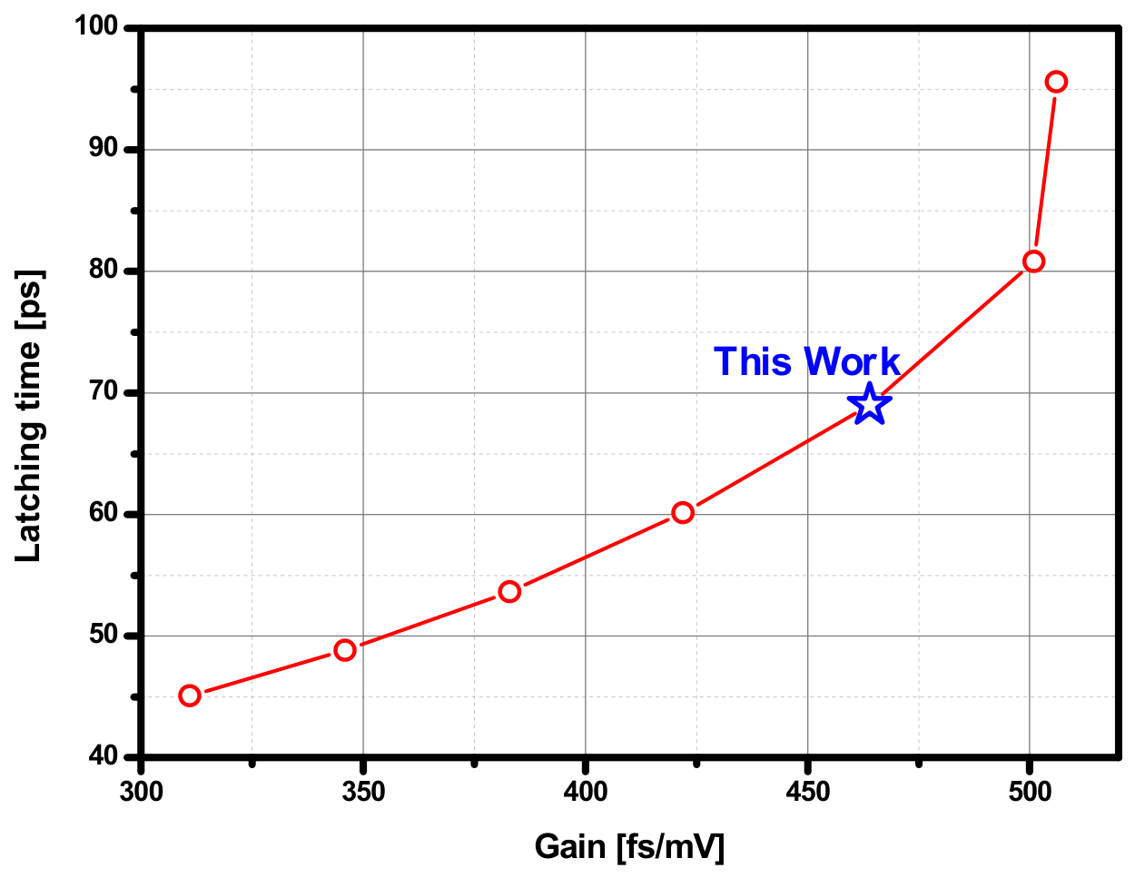
Here, I k + and I k are the discharge currents of the DA output nodes determined by the input voltage, C l o a d is the load capacitance at the DA output nodes, and V D T is the voltage difference between VDD and the inverter logic threshold. t 1 and t 2 are the corresponding discharge times from VDD to the inverter logic threshold, g m is the transconductance of the input transistors, and I t a i l is the total tail current of the DA. These definitions and the voltage-to-time gain expression follow [23]. Although these relationships were originally derived for the DA, the active amplification phase of the CDA employed in this work is also based on a dynamic differential-pair charging or discharging operation. Therefore, the relationships in (1) and (2) are used as design guidelines for analyzing the CDA time-domain gain. Since the output transition time and the time-domain gain depend on common circuit parameters, the gain–latching-time characteristic of the CDA was evaluated through post-layout simulations. As shown in Figure 11, the latching time increases with the CDA time-domain gain. In this work, the CDA was designed to provide a time-domain gain of approximately 464 fs/mV, with a corresponding latching time of approximately 69 ps.

4. Measurement Results

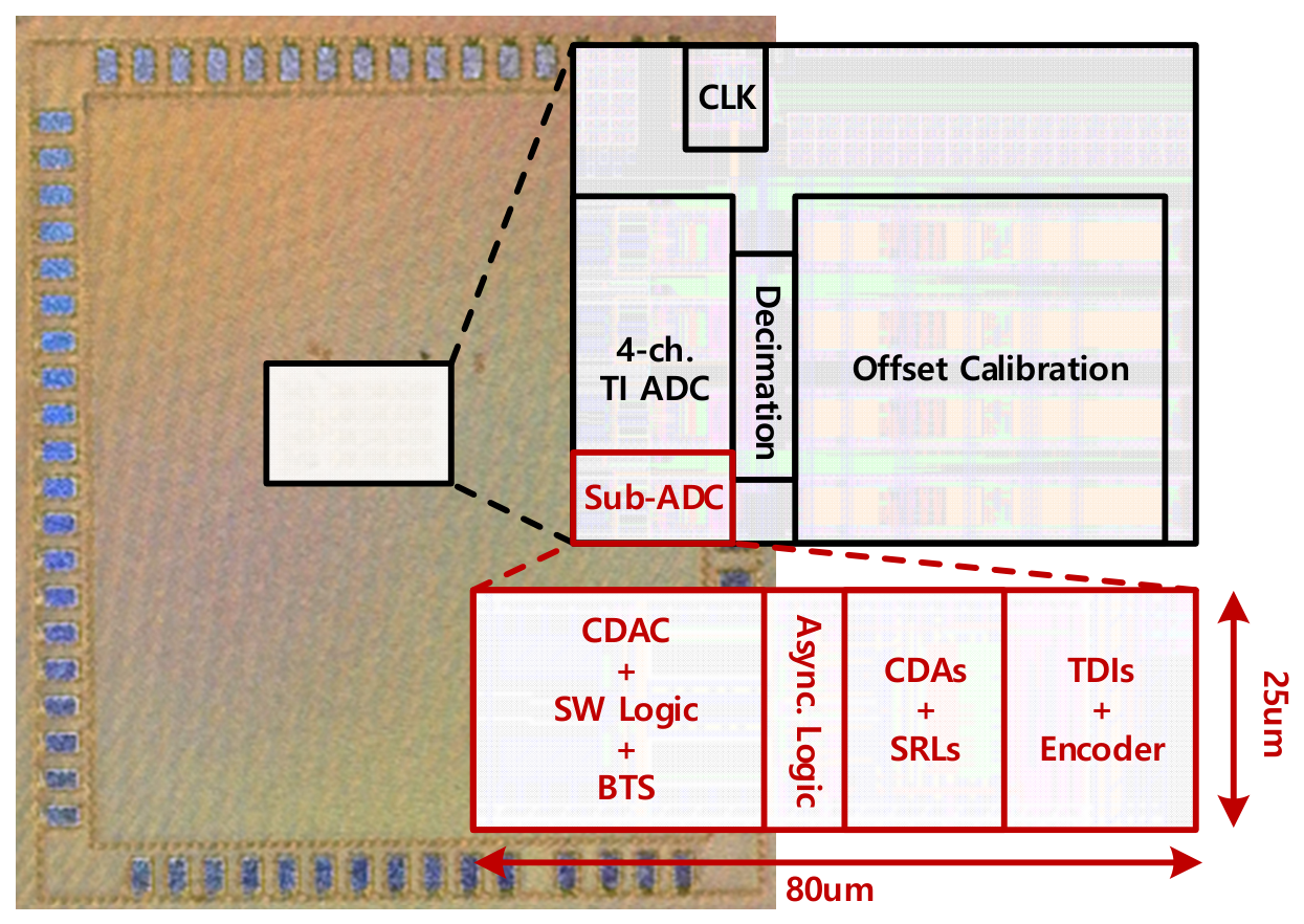
The proposed 3.2 GS/s 8-bit four-channel TI SAR-Flash ADC was fabricated in a 28 nm CMOS process. Figure 12 shows the die photograph and enlarged layout views of the ADC core and a single sub-ADC. Each sub-ADC occupies 80 μm × 25 μm and consists of a CDAC with switch logic, asynchronous logic, four CDAs and SRLs, a TDI array, and encoder blocks. The four-channel ADC core, including power routing, occupies 232 μm × 97 μm, corresponding to an area of approximately 0.023   mm 2 .
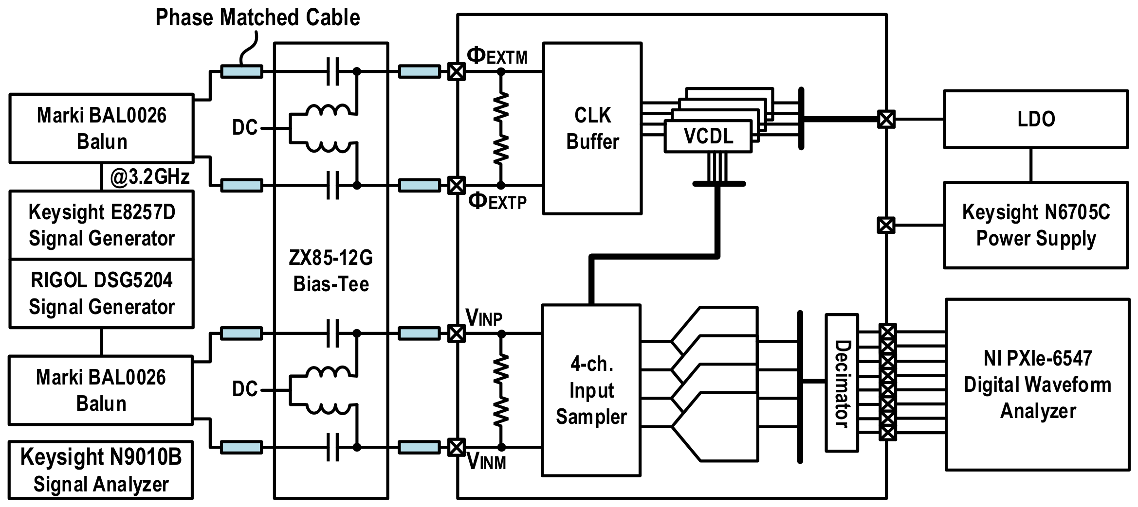
The measurement environment for the 3.2 GS/s TI ADC is illustrated in Figure 13. The clock and analog input signals are generated by Keysight Technologies E8257D-540 (Keysight Technologies, Santa Rosa, CA, USA) and RIGOL DSG5204 (RIGOL Technologies, Suzhou, China) signal generators, respectively. These signals are converted to differential inputs via Marki BAL0026 (Marki Microwave LLC, Morgan Hill, CA, USA) baluns and fed into the chip through Mini-Circuits ZX85-12G bias-tees (Mini-Circuits, Brooklyn, NY, USA). Phase-matched cables are used to maintain 100 Ω differential impedance matching. Additionally, a Keysight Technologies N9010B (Keysight Technologies, Santa Rosa, CA, USA) signal analyzer is utilized to monitor the input signal spectrum. On the output side, the decimated digital outputs are captured by an NI PXIe-6547 digital waveform analyzer (National Instruments Corporation, Austin, TX, USA), enabling real-time performance evaluation and detection of inter-channel mismatches, including offset and timing skew.
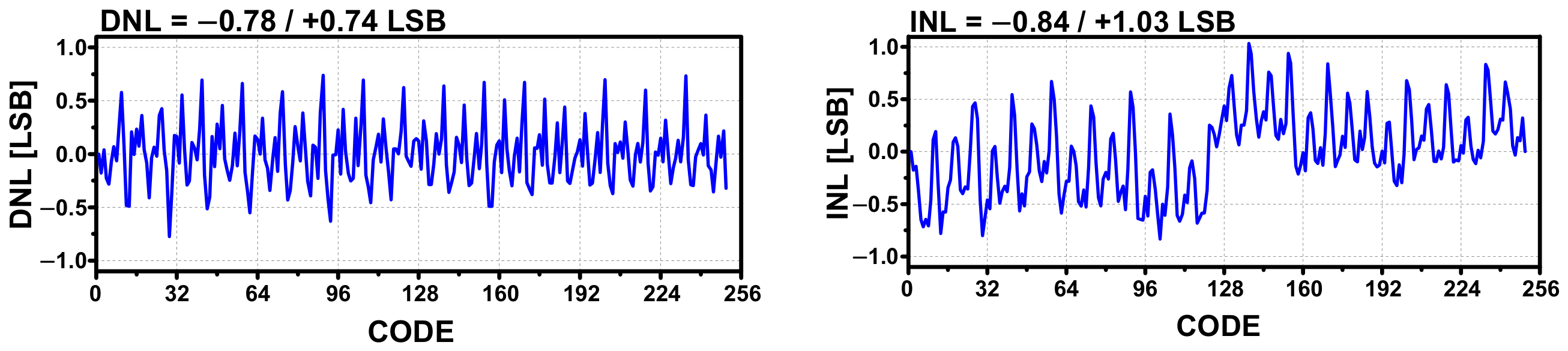
The measured differential non-linearity (DNL) and integral non-linearity (INL) at 3.2 GS/s are shown in Figure 14. After offset calibration, the measured DNL and INL range from −0.78 to +0.74 LSB and from −0.84 to +1.03 LSB, respectively. Since the measured DNL remains within ±1 LSB, the ADC achieves no missing codes after calibration. The measured INL also remains close to 1 LSB, confirming that the proposed ADC maintains sufficient static linearity at the target sampling rate.
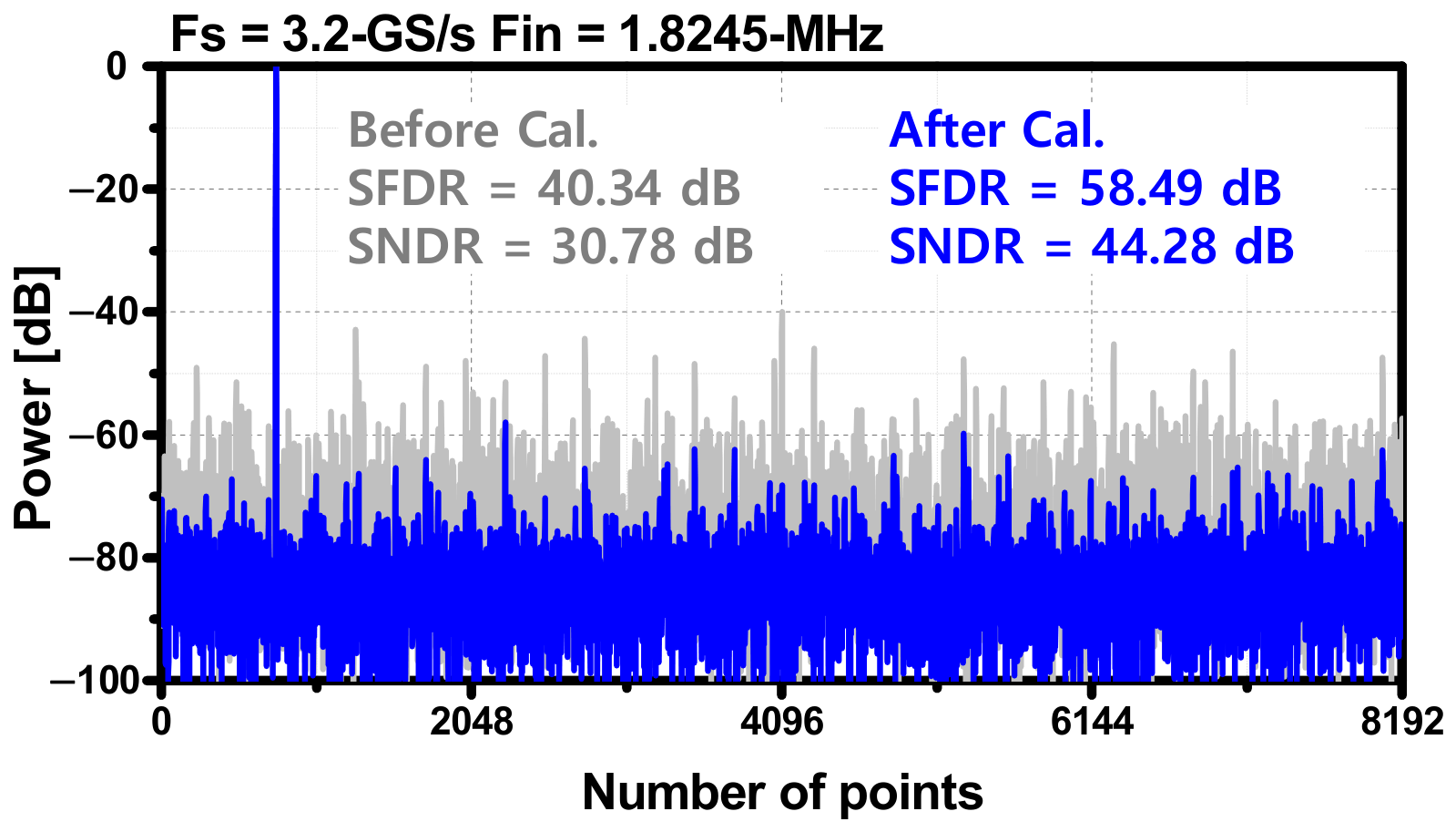
Figure 15 shows the fast Fourier transform (FFT) spectra with and without offset calibration for a 1.8245 MHz input at a 3.2 GS/s conversion rate. With calibration, the spurious-free dynamic range (SFDR) improves from 40.34 dB to 58.49 dB, and the signal-to-noise and distortion ratio (SNDR) improves from 30.78 dB to 44.28 dB.
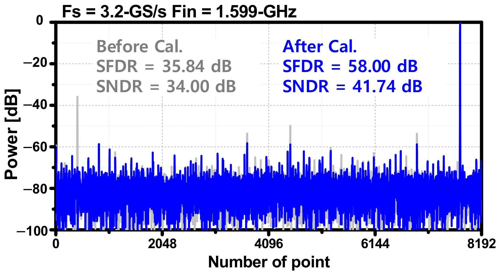
Figure 16 shows the FFT spectra for a Nyquist-rate input before and after timing-skew calibration. Before calibration, the SFDR and SNDR are 35.84 dB and 34.02 dB, respectively. The timing-skew error is estimated to be approximately 1.61 ps based on the worst-case spur [25]. After calibration, these spurs are significantly suppressed, and the SFDR and SNDR improve to 58.03 dB and 41.74 dB, respectively. These results demonstrate that the proposed timing-skew calibration effectively reduces channel-to-channel sampling-time mismatch and enables the ADC to maintain stable conversion performance even for high-frequency input signals close to the Nyquist frequency.
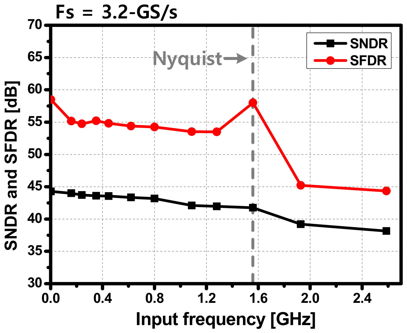
Figure 17 shows the performance as a function of input frequency at a 3.2 GS/s conversion rate. As the input frequency increases from 1.8245 MHz to the Nyquist frequency, the SNDR remains above 41 dB. It is noted that the relatively higher SNDR observed at the lowest input frequency and at the Nyquist frequency is mainly due to differences in the measurement equipment and external filters, which reduce the second-harmonic component and thereby improve the measured performance.
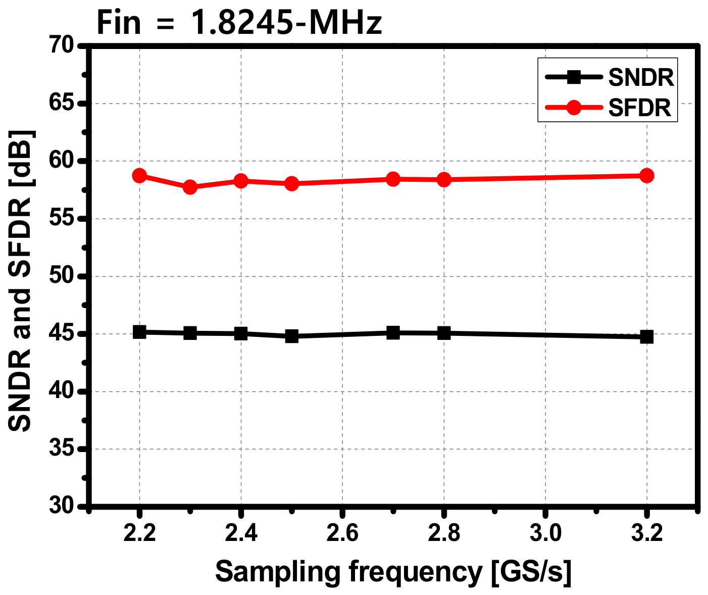
Figure 18 shows the performance for a 1.8245 MHz input as the sampling rate is varied from 2.2 to 3.2 GS/s. In this case, the SNDR remains above 44 dB over the entire sampling-rate range. The ADC core operates from a 1 V supply.
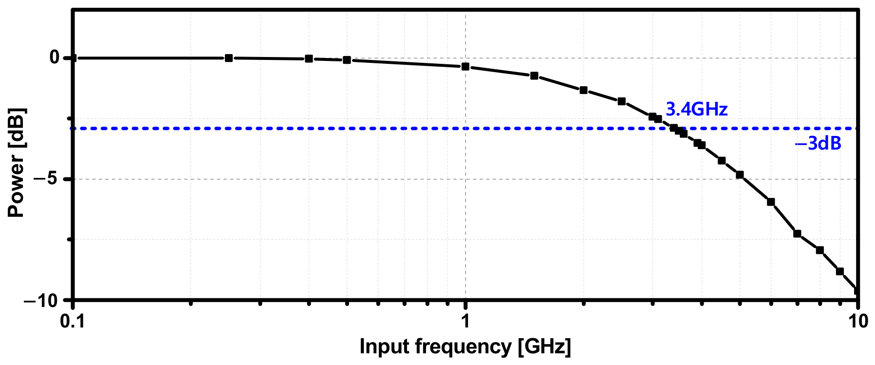
Figure 19 shows the measured input-frequency response of the four-channel TI ADC. The hold capacitance is 64 fF, as determined from the KT/C noise requirement, and approximately 23 fF of additional parasitic capacitance is associated with the input routing to the four TI channels. The measured input response also reflects the effects of the I/O pad capacitance and impedance-matching resistance. The measured −3 dB input bandwidth is approximately 3.4 GHz, which is sufficiently higher than the 1.6-GHz Nyquist frequency at the target sampling rate of 3.2 GS/s.
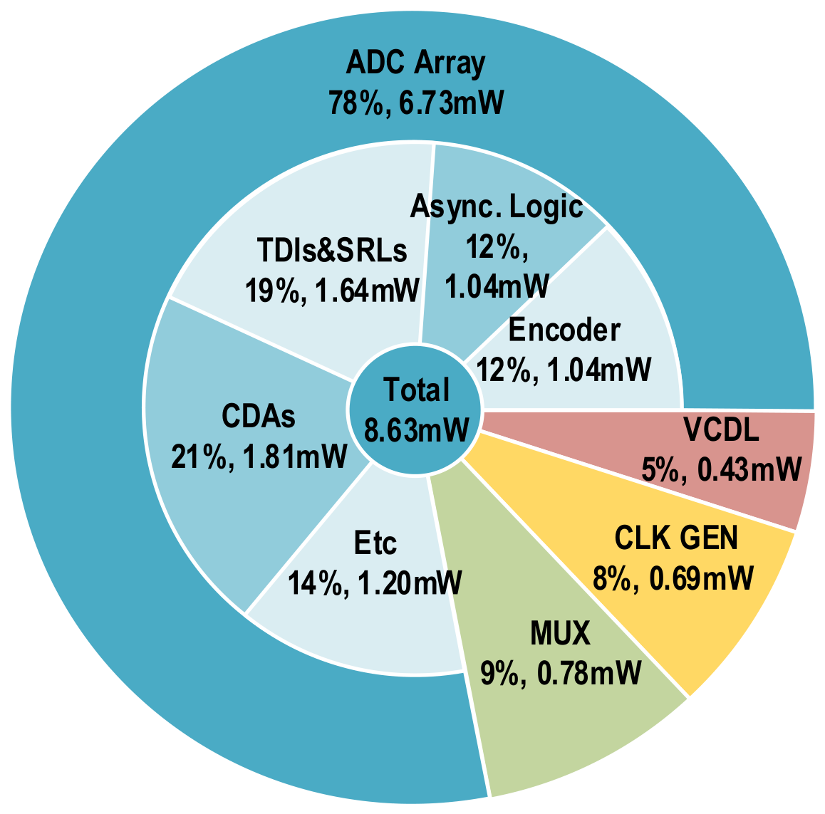
At 3.2 GS/s, the total power consumption is 8.63 mW, and the power breakdown is shown in Figure 20. The ADC array occupies the largest portion, consuming 6.73 mW, which corresponds to 78% of the total power. Within the ADC array, the CDAs consume 1.81 mW, followed by the TDIs and SR latches with 1.64 mW, the asynchronous logic and encoder with 1.04 mW each, and the remaining circuits with 1.20 mW. The VCDL, clock generator, and MUX consume 0.43 mW, 0.69 mW, and 0.78 mW, respectively.
Table 1 compares the proposed ADC with recently reported TI ADCs having 6- to 8-bit resolution and sampling rates ranging from 2 to 3.6 GS/s. These criteria were selected to compare ADCs operating in a similar resolution and sampling-rate range. The proposed ADC achieves 3.2 GS/s operation with an 8-bit resolution using a four-channel TI architecture. Although the number of interleaved channels is relatively small, the proposed ADC maintains high Nyquist performance, achieving an SNDR of 41.74 dB, an SFDR of 58.03 dB, and an effective number of bits (ENOB) of 6.64 bits. Furthermore, the measured Walden figure-of-merit (FoM) is 27 fJ/conv.-step, which is the lowest value among the compared ADCs. This shows that the proposed architecture provides an efficient resolution–speed–power trade-off while maintaining a compact active area.

5. Conclusions

This paper has presented a 28 nm CMOS 8-bit 3.2 GS/s four-channel TI SAR-Flash hybrid ADC employing CDA-based two-step sub-ADCs with LU-SAR and reference-embedded I-Flash operation. By reusing only four CDAs over a 4-bit LU-SAR and 4.5-bit I-Flash conversion and operating them on both clock edges, the sub-ADC achieves full 8-bit resolution with reduced comparator count and input capacitance, improving energy and area efficiency. A four-channel TI architecture with a multi-phase clock generator and VCDL-based phase alignment enables 3.2 GS/s operation while relaxing the per-channel clock frequency and supporting foreground offset calibration under realistic TI loading conditions. The prototype ADC achieves DNL/INL within −0.78/+0.74 LSB and −0.84/+1.03 LSB and delivers SNDR/SFDR of approximately 44.28/58.49 dB at a low-frequency input and 41.74/58.03 dB at a Nyquist-rate input, corresponding to ENOB of about 7.1 and 6.6 bits. Operating from a 1 V supply, the ADC core consumes 8.63 mW at 3.2 GS/s, resulting in a Walden FoM of about 27 fJ/conversion step. These results demonstrate that the proposed CDA-based SAR-Flash hybrid ADC provides a compact and power-efficient solution for multi-GS/s medium-resolution data conversion in high-speed communication systems.

Author Contributions

Conceptualization, D.-R.O., D.-J.C. and D.-Y.K.; methodology, D.-R.O., D.-J.C. and S.-W.O.; investigation, D.-R.O.; resources, D.-R.O., S.-W.O., H.-G.H., Y.-W.Y., W.-S.S., J.-M.K., Y.-S.J. and D.-Y.K.; writing—original draft preparation, D.-R.O., D.-J.C. and D.-Y.K.; writing—review and editing, D.-R.O., D.-J.C. and S.-W.O. All authors have read and agreed to the published version of the manuscript.

Funding

This research was supported by the ANCHOR program through the Jeju ANCHOR center, funded by the Ministry of Education (MOE) and the Jeju Special Self-Governing Province, Republic of Korea (2026-ANCHOR-17-001).

Data Availability Statement

The original contributions presented in this study are included in the article. Further inquiries can be directed to the corresponding author.

Acknowledgments

The chip fabrication and EDA tools were supported by the IC Design Education Center (IDEC), Republic of Korea. The ADC samples were analyzed using a signal analyzer (Keysight Technologies N9010B, NFEC-2026-07-317140) and an analog signal generator (Keysight Technologies E8257D-540, NFEC-2026-07-317139), Center for Research Facilities (CRIEF) at Jeju National University. Additionally, an RF signal generator (RIGOL DSG5204, NFEC-2025-02-303691) was utilized, supported by the Korea Basic Science Institute (National Research Facilities and Equipment Center) grant funded by the Korean government (MSIT) (No. RS-2024-00404783).

Conflicts of Interest

The authors declare no conflicts of interest.

Abbreviations

The following abbreviations are used in this manuscript:
ADCAnalog-to-Digital Converter
TITime-Interleaved
CDAComplementary Dynamic Amplifier
CDACCapacitive Digital-to-Analog Converter
LVDSLow-Voltage Differential Signaling
VCDLVoltage-Controlled Delay Line
LULoop-Unrolled
SARSuccessive Approximation Register
I-FlashInterpolating Flash
BTSBootstrapped Switches
SRLSR-Latch
STPShoot-Through-Prevention
TDITime-Domain Interpolators
DFFD Flip Flop
DNLDifferential Nonlinearity
INLIntegral Nonlinearity
FFTFast Fourier Transform
SFDRSpurious-Free Dynamic Range
SNDRSignal-to-Noise and Distortion Ratio
ENOBEffective Number of Bits
FoMFigure-of-Merit

References

  1. Li, X.; Wang, R.; He, L.; Yoshioka, K. A High-Speed 8-Bit Single-Channel SAR ADC with Tailored Bit Intervals and Split Capacitors. Electronics 2025, 14, 2032. [Google Scholar] [CrossRef] [Scilit]
  2. Lee, E.; Lee, S.; Pyo, C.; Kim, H.; Han, J. A 2-GS/s 6-bit Single-channel Speculative Loop-unrolled SAR ADC with Low-overhead Comparator Offset Calibration in 28-nm CMOS. J. Semicond. Technol. Sci. 2024, 24, 355–364. [Google Scholar] [CrossRef] [Scilit]
  3. Krupnik, Y.; Perelman, Y.; Levin, I.; Sanhedrai, Y.; Eitan, R.; Khairi, A. 112-Gb/s PAM4 ADC-Based SERDES Receiver with Resonant AFE for Long-Reach Channels. IEEE J. Solid-State Circuits 2020, 55, 1077–1085. [Google Scholar] [CrossRef] [Scilit]
  4. Bheemisetti, C.; Pandey, K.; Lotan, I.; Ori, G.; Khairi, A.; Krupnik, Y. A 7-bit 1.75-GS/s 6.9-fJ/conv.-step FoMw Loop-Unrolled Fully Asynchronous SAR ADC in 3-nm CMOS for a 224-Gb/s SerDes Receiver. IEEE J. Solid-State Circuits 2025, 60, 1486–1499. [Google Scholar] [CrossRef] [Scilit]
  5. Kull, L.; Luu, D.; Menolfi, C.; Brändli, M.; Francese, P.A.; Morf, T. A 24–72-GS/s 8-b Time-Interleaved SAR ADC with 2.0–3.3-pJ/Conversion and >30 dB SNDR at Nyquist in 14-nm CMOS FinFET. IEEE J. Solid-State Circuits 2018, 53, 3508–3516. [Google Scholar] [CrossRef] [Scilit]
  6. Jang, S.-Y.; Lee, J.-W.; Choi, Y.-J.; Kim, D.-G.; Kim, G. Recent Advances in Ultrahigh-Speed Wireline Receivers with ADC-DSP-Based Equalizers. IEEE Open J. Solid-State Circuits Soc. 2024, 4, 290–304. [Google Scholar] [CrossRef] [Scilit]
  7. Greshishchev, Y.M.; Aguirre, J.; Besson, M.; Gibbins, R.; Falt, C.; Flemke, P. A 40-GS/s 6-b ADC in 65-nm CMOS. In Proceedings of the IEEE International Solid-State Circuits Conference (ISSCC), San Francisco, CA, USA, 7–11 February 2010; pp. 390–391. [Google Scholar]
  8. Kull, L.; Pliva, J.; Toifl, T.; Schmatz, M.; Francese, P.A.; Menolfi, C. A 110 mW 6-bit 36 GS/s Interleaved SAR ADC for 100 GBE Occupying 0.048 mm2 in 32-nm SOI CMOS. In Proceedings of the IEEE Asian Solid-State Circuits Conference (A-SSCC), Kaohsiung, Taiwan, 10–12 November 2014; pp. 89–92. [Google Scholar]
  9. Oh, D.-R.; Kim, J.-I.; Seo, M.-J.; Kim, J.-G.; Ryu, S.-T. A 6-bit 10-GS/s 63-mW 4× Time-Domain Interpolating Flash ADC in 65-nm CMOS. In Proceedings of the IEEE European Solid-State Circuits Conference (ESSCIRC), Graz, Austria, 14–18 September 2015; pp. 323–326. [Google Scholar]
  10. Xu, B.; Zhou, Y.; Chiu, Y. A 23-mW 24-GS/s 6-bit Voltage-Time Hybrid Time-Interleaved ADC in 28-nm CMOS. IEEE J. Solid-State Circuits 2017, 52, 1091–1100. [Google Scholar] [CrossRef] [Scilit]
  11. Gestsson, H.H.; Thorbergsson, H.; Andersen, K.; Unnthorsson, R. Adjustable ON-TIME Delay TI-ADC via Dual-Slope PWM and Four-Phase Binary Up/Down Counter. Electronics 2026, 15, 1634. [Google Scholar] [CrossRef] [Scilit]
  12. Wang, C.; Yang, Z.; Xing, X.; Duan, Q.; Zheng, X.; Gielen, G. A 10-Bit 400 MS/s Dual-Channel Time-Interleaved SAR ADC Based on Comparator Multiplexing. Electronics 2023, 12, 4062. [Google Scholar] [CrossRef] [Scilit]
  13. Lim, J.-H.; Park, S.-G. A Simple Timing-skew Calibration Using Flip-flops for Time-interleaved ADCs. J. Semicond. Technol. Sci. 2023, 23, 89–97. [Google Scholar] [CrossRef] [Scilit]
  14. Oh, S.-W.; Oh, D.-R. Two-rank Decimation Technique for High-speed Time-interleaved Analog-to-digital Converters. J. Semicond. Technol. Sci. 2025, 25, 284–291. [Google Scholar] [CrossRef] [Scilit]
  15. Chung, Y.-H.; Wu, J.-T. A 16-mW 8-bit 1-GS/s Digital-Subranging ADC in 55-nm CMOS. IEEE Trans. Very Large Scale Integr. (VLSI) Syst. 2015, 23, 557–566. [Google Scholar] [CrossRef] [Scilit]
  16. Yang, X.; Liu, J. A 10-GS/s 6-bit Time-Interleaved Partially Active Flash ADC. IEEE Trans. Circuits Syst. I Regul. Pap. 2014, 61, 2272–2280. [Google Scholar] [CrossRef] [Scilit]
  17. El-Chammas, M.; Murmann, B. A 12-GS/s 81-mW 5-bit Time-Interleaved Flash ADC With Background Timing Skew Calibration. IEEE J. Solid-State Circuits 2011, 46, 838–847. [Google Scholar] [CrossRef] [Scilit]
  18. Kiran, S.; Cai, S.; Zhu, Y.; Hoyos, S.; Palermo, S. Digital Equalization With ADC-Based Receivers: Two Important Roles Played by Digital Signal Processing in Designing Analog-to-Digital-Converter-Based Wireline Communication Receivers. IEEE Microw. Mag. 2019, 20, 62–79. [Google Scholar] [CrossRef] [Scilit]
  19. Frans, Y.; Shin, J.; Zhou, L.; Upadhyaya, P.; Im, J.; Kireev, V. A 56-Gb/s PAM4 Wireline Transceiver Using a 32-Way Time Interleaved SAR ADC in 16-nm FinFET. IEEE J. Solid-State Circuits 2017, 52, 1101–1110. [Google Scholar] [CrossRef] [Scilit]
  20. Sun, K.; Wang, G.; Zhang, Q.; Elahmadi, S.; Gui, P. A 56-GS/s 8-bit Time-Interleaved ADC with ENOB and BW Enhancement Techniques in 28-nm CMOS. IEEE J. Solid-State Circuits 2019, 54, 821–833. [Google Scholar] [CrossRef] [Scilit]
  21. Huang, C.-C.; Wang, C.-Y.; Wu, J.-T. A CMOS 6-bit 16-GS/s Time-Interleaved ADC Using Digital Background Calibration Techniques. IEEE J. Solid-State Circuits 2011, 46, 848–858. [Google Scholar] [CrossRef] [Scilit]
  22. Oh, D.-R.; Moon, K.-J.; Park, Y.-H.; Lee, K.-H.; Park, S.-J.; Lee, S.-N.; Hwang, H.-C.; Shin, H.-C.; Cho, Y.-J.; Choi, M.; et al. An 8-bit 1-GS/s Asynchronous Loop-Unrolled SAR-Flash ADC with Complementary Dynamic Amplifiers in 28-nm CMOS. IEEE J. Solid-State Circuits 2021, 56, 1216–1226. [Google Scholar] [CrossRef] [Scilit]
  23. Oh, D.-R.; Kim, J.-I.; Jo, D.-S.; Kim, W.-C.; Chang, D.-J.; Ryu, S.-T. A 65-nm CMOS 6-bit 2.5-GS/s 7.5-mW 8× Time-Domain Interpolating Flash ADC with Sequential Slope-Matching Offset Calibration. IEEE J. Solid-State Circuits 2019, 54, 288–297. [Google Scholar] [CrossRef] [Scilit]
  24. Moon, K.-J.; Oh, D.-R.; Park, Y.-H.; Lee, K.-H.; Park, S.-J.; Lee, S.-N.; Hwang, H.-C.; Shin, H.-C.; Cho, Y.-J.; Choi, M.; et al. A 12-bit 10-GS/s 16-channel Time-Interleaved ADC With a Digital Processing Timing-Skew Background Calibration in 5-nm FinFET. In Proceedings of the IEEE Symposium on VLSI Technology and Circuits, Honolulu, HI, USA, 13–17 June 2022; pp. 172–173. [Google Scholar]
  25. Razavi, B. Design Considerations for Interleaved ADCs. IEEE J. Solid-State Circuits 2013, 48, 1806–1817. [Google Scholar] [CrossRef] [Scilit]
  26. Wang, D.; Zhu, X.; Guo, X.; Luan, J.; Zhou, L.; Wu, D.; Liu, H.; Wu, J.; Liu, X. A 2.6 GS/s 8-Bit Time-Interleaved SAR ADC in 55 nm CMOS Technology. Electronics 2019, 8, 305. [Google Scholar] [CrossRef] [Scilit]
  27. Li, D.; Qian, M.; Li, D.; Liang, H.; Zhu, Z. A 2.6-GS/s 8-bit Time-Interleaved ADC With Fully Dynamic Current Integrating Sampler. IEEE Solid-State Circuits Lett. 2025, 8, 29–32. [Google Scholar] [CrossRef] [Scilit]
  28. Seong, K.; Han, J.-S.; Shim, Y.; Baek, K.-H. A 2.5 GS/s 7-Bit 5-Way Time-Interleaved SAR ADC With On-Chip Background Offset and Timing-Skew Calibration. IEEE Trans. Circuits Syst. II Express Briefs 2022, 69, 4043–4047. [Google Scholar] [CrossRef] [Scilit]
  29. Kim, C.; Park, S.; Shim, M.; Lee, W.; Choi, Y.; Kim, H. A 6-bit 3.6-GS/s 4-Channel Time-Interleaved ADC with Front-Rank MSB Decision and 2-Then-1.5-bit/Cycle Architecture. IEEE Trans. Circuits Syst. I Regul. Pap. 2026, 73, 4533–4544. [Google Scholar] [CrossRef] [Scilit]
  30. Jiang, W.; Zhu, Y.; Chan, C.-H.; Murmann, B.; Martins, R.P. A 7-bit 2 GS/s Time-Interleaved SAR ADC With Timing Skew Calibration Based on Current Integrating Sampler. IEEE Trans. Circuits Syst. I Regul. Pap. 2021, 68, 557–568. [Google Scholar] [CrossRef] [Scilit]
  31. Wang, J.; Gao, Z.; Cheng, X.; Wang, J.; Li, Z.; Han, J.; Zeng, X. A 1.6 GS/s 42.6-dB SNDR Synthesis Friendly Time-Interleaved SAR ADC Using Metastability Detection and Escape Acceleration Technique. IEEE Trans. Circuits Syst. II Express Briefs 2024, 71, 1859–1863. [Google Scholar] [CrossRef] [Scilit]
  32. Li, D.; Zhao, X.; Shen, Y.; Liu, S.; Zhu, Z. A 7-bit 3.8-GS/s 2-Way Time-Interleaved 4-bit/Cycle SAR ADC 16× Time-Domain Interpolation in 28-nm CMOS. IEEE Trans. Circuits Syst. I Regul. Pap. 2023, 70, 3557–3568. [Google Scholar] [CrossRef] [Scilit]
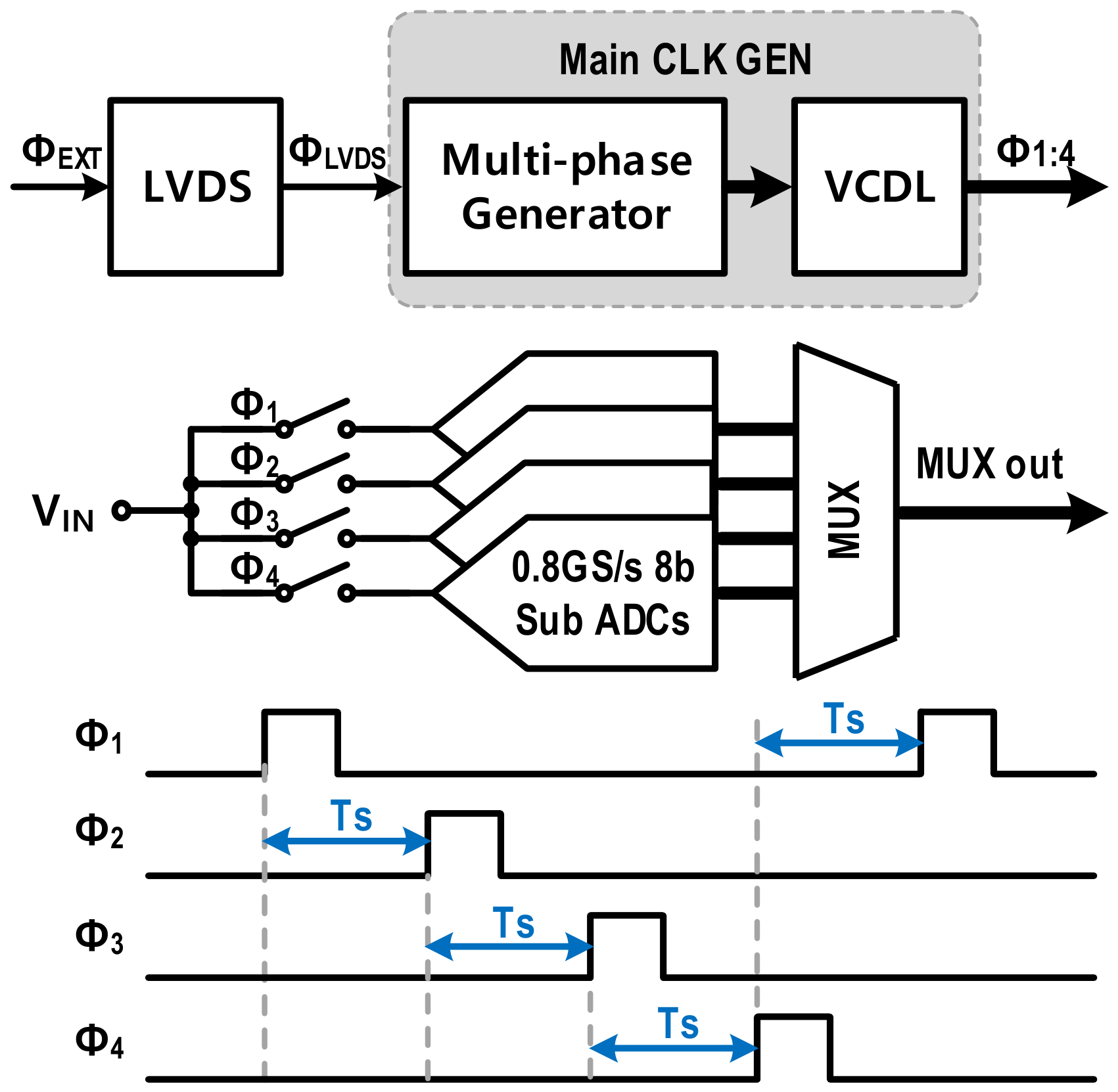
Figure 1. Overall architecture of the proposed four-channel TI ADC.
Electronics 15 04232 g001
Figure 2. Block diagram of the proposed TI sub-ADC.
Electronics 15 04232 g002
Figure 3. (a) CDA circuit diagram, (b) asynchronous clock timing diagram.
Electronics 15 04232 g003
Figure 4. Main clock generator. (a) Multi-phase generation logic. (b) Timing diagram.
Electronics 15 04232 g004
Figure 5. Timing-skew calibration procedure for a four-channel TI ADC [24].
Electronics 15 04232 g005
Figure 6. Behavioral simulation results with Monte Carlo-derived timing-skew distribution. (a) Channel timing skew before and after calibration. (b) SNDR before and after calibration.
Electronics 15 04232 g006
Figure 7. VCDL circuit and timing diagram.
Electronics 15 04232 g007
Figure 8. Foreground offset-calibration sequence.
Electronics 15 04232 g008
Figure 9. Foreground offset-calibration block diagram.
Electronics 15 04232 g009
Figure 10. Simulated ZX points of the CDA<4> under PVT variation.
Electronics 15 04232 g010
Figure 11. Simulated CDA latching time versus time-domain gain.
Electronics 15 04232 g011
Figure 12. Die photograph.
Electronics 15 04232 g012
Figure 13. Measurement setup.
Electronics 15 04232 g013
Figure 14. Measured DNL and INL.
Electronics 15 04232 g014
Figure 15. Measured FFT spectra at 3.2 GS/s. Before and after offset calibration with a 1.8245 MHz.
Electronics 15 04232 g015
Figure 16. Measured FFT spectra at a 3.2 GS/s sampling rate with a 1.599-GHz input.
Electronics 15 04232 g016
Figure 17. Measured SNDR and SFDR versus various input frequencies at 3.2 GS/s.
Electronics 15 04232 g017
Figure 18. Measured SNDR and SFDR versus various conversion rates with a 1.8245 MHz input frequency.
Electronics 15 04232 g018
Figure 19. Measured input bandwidth of the ADC at 3.2 GS/s.
Electronics 15 04232 g019
Figure 20. Power breakdown.
Electronics 15 04232 g020
Table 1. Performance comparison.
This WorkRef. [26]Ref. [27]Ref. [28]Ref. [29]Ref. [30]Ref. [31]Ref [32]
Technology (nm)2855652828282828
ArchitectureTI SAR-FlashTI ADCTI ADCTI ADCTI ADCTI SARTI SARTI ADC
# of channels48854442
Supply (V)11.21.20.911.2/0.911
Resolution (bit)88876787
FS (GS/s)3.22.62.62.53.621.63.8
DNL/INLMAX (LSB)0.78/1.030.93/0.910.75/1.070.45/0.350.67/0.660.98/1.51.34/1.530.55/0.73
SNDR@Nyq. (dB)41.7431.841.294033.936.442.639.9
SFDR@Nyq. (dB)58.0340.350.0152.349.847.852.950.8
ENOB@Nyq. (bit)6.6456.576.35.35.756.786.34
Power (mW)8.636028.887.66.17.623.227.5
Active area (mm2)0.023 20.2200.4000.0300.0190.0080.0190.008 2
Walden FOM 1
(fJ/conv.-step)
27726117.237.241.870.818.324.4
1 Walden FoM = Power/(2ENOB  × Sampling frequency), 2 w/o calibration.
Disclaimer/Publisher’s Note: The statements, opinions and data contained in all publications are solely those of the individual author(s) and contributor(s) and not of MDPI and/or the editor(s). MDPI and/or the editor(s) disclaim responsibility for any injury to people or property resulting from any ideas, methods, instructions or products referred to in the content.