Article

Blocking State-Enabled Induction Heating in Bipolar Transistors

by
Roberto Baca-Arroyo
Department of Electronics, National Polytechnic Institute, School of Mechanical and Electrical Engineering, México City 07738, Mexico
Electronics 2026, 15(17), 4022; https://doi.org/10.3390/electronics15174022
Submission received: 8 August 2026 / Revised: 3 September 2026 / Accepted: 4 September 2026 / Published: 5 September 2026
(This article belongs to the Section Power Electronics)

Abstract

This work presents a solution for induction heating application using a blocking circuit, the significant advantages of which include power conversion using a single switch and adjustable heat conversion in the absence of a driver circuit. Equations governing circuit operation are derived based on empirical concepts used to explain the conduction states. Physics-based analytic models are presented to learn how an induction coil behaves depending on its geometry and ability to heat transfer toward a low-grade ferrous composite used as the target material, and the bipolar transistor depending on its junction temperature upon space-charge-limited conduction by ionized donor and acceptor impurities. Blocking state-dependent current–voltage characteristics define an iterative design strategy. Experimental results taken from a laboratory prototype built with a commercial NPN Silicon Power Transistor from ON Semiconductor (with part number MJE13005G, Scottsdale, AZ, USA) confirm that temperature adjustments in the heated target when the blocking state changes can be managed from an external resistor connected to the bipolar transistor.

1. Introduction

Induction heating (IH) is of great interest from the perspective of innovative circuit design strategies, where IH can be classified as a wireless power transfer (WPT) technology used in many industrial, domestic, and medical applications [1]. It is based on coupling phenomena between an induction coil and a ferromagnetic material like iron and its alloys, which have low resistivity and high permeability, with values from 100 to 500. Nevertheless, it can result in unintended human electromagnetic field (EMF) exposure characterized by shallow penetration at specific absorption rates into closed environments [2]. From a safety perspective, the contribution of EMF emissions is generally smaller and therefore not the dominant EMF exposure source compared to applications in which they are generated by coupling structures; however, with new evidence, there is a trend toward scaling operating frequencies to greater than 300 kHz up to several MHz. Therefore, further challenges in determining optimized engineering solutions for IH applications are expected, for example, in accurate local heating of biological tissues [1,3].
Two different converter strategies for induction heating are taken into account: resonant converters and single-switch converters. In the first strategy, IGBT and MOSFET devices are commonly used. From Table 1, it can be concluded that their driver technology uses complex signal processing to support medium- and higher-power applications; however, in accordance with semiconductor technology, power losses are usually lower under switching regime at frequencies ranging from 20 kHz to 1 MHz. In the second strategy, driver technologies can be focused on analog and digital signal processing or hybrid methods to support low- and medium-power applications and to operate at frequencies lower than 500 kHz, where power losses are negligible in MOSFET, in accordance with their switching times and lower ON-resistance values. However, in commercial BT devices, the power losses must be taken into account.
The main advantage of resonant converters is that the dominant heating principle is based on eddy-current phenomena, in which the induction targets commonly used are non-ferrous metals (aluminum and copper) heated to temperatures > 100   ° C . However, a major disadvantage is that due to the Joule effect, eddy currents are converted to heat energy that does not dissipate easily. Additionally, induction heating can be created if ferromagnetic materials are used and single-switch converters are chosen.
It has been documented that due to their high resistivity and low permeability, linear conductive materials such as aluminum, copper, and other non-ferrous metals are generally unsuitable for low-power IH applications in the absence of ferromagnetic materials [2]. However, other applications, such as in non-invasive treatment devices used for electromagnetic heating in cancer treatment therapy, those used for local heating to target tumors and infections around implants, and those made with low-resistivity metals to minimize damage to healthy tissue while maximizing the therapeutic impact, are now of research interest. It is desirable to design a novel adjustable heating source that allows special ferromagnetic metals to be homogenously heated and placed in the area needing clinic treatment, where the induction depth can be driven through a specific inductor chosen to allow short heating times at temperatures close to 50 °C [4].
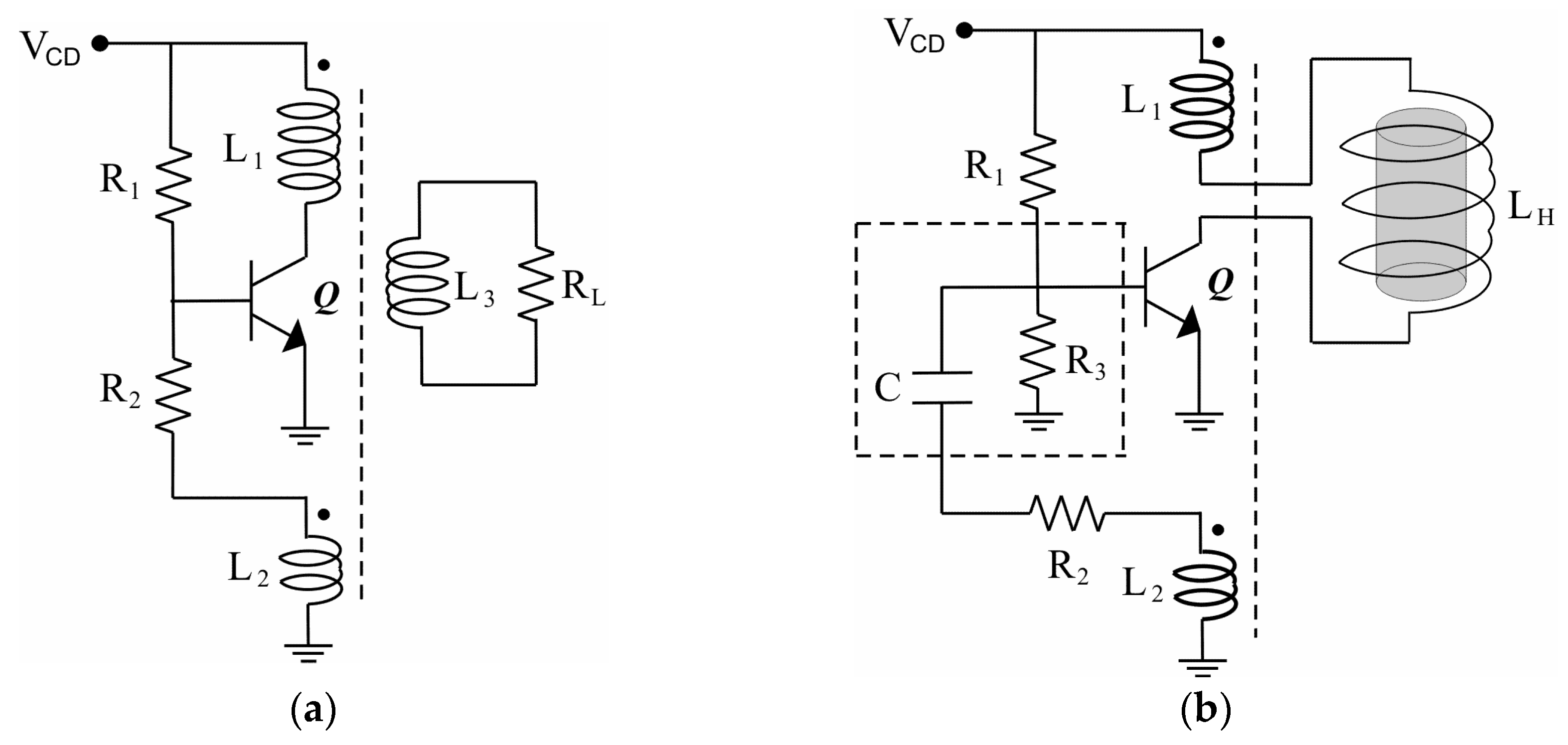
The blocking circuit shown in Figure 1a has been previously applied for power conversion in switching-mode power supplies [5]. It comprises one transformer whose primary winding is connected in series with the collector while its secondary winding is connected in series with a resistor,   R 2 and with the base in the bipolar transistor (BT). A trigger current source passing through the resistor, R 1 , serves as startup forward bias across the base–emitter junction. In order to demonstrate that the blocking state in a bipolar transistor is suitable for power conversion of adjustable heat energy, this work highlights several advantages of the blocking circuit, such as its low power consumption, lack of a driver circuit, and temperature adjustment ability in a single power stage of conversion in comparison with the well-known half-bridge series resonant circuits that provide the most efficient energy conversion by minimizing switching losses.
Such resonant converters comprise a complex control circuit, an input current detection circuit, a resonant current detection circuit, and a gate driver circuit for the switching of metal–oxide–semiconductor field-effect transistors (MOSFETs) or insulated-gate bipolar transistors (IGBT) in multiple-switch high-frequency inverters [3,6]. An induction coil, L H , and a passive circuit comprising a series-connected coupling capacitor, C , and a resistor, R 3 , parallelly connected in the base–emitter junction of the BT enable the proposed blocking circuit shown in Figure 1b for low-power IH applications to emerge as a practical clinic treatment device.
This paper is divided into the following sections: Section 2 describes the operating modes involved in the proposed blocking circuit through transient analysis to validate the equations governing different conduction states. Using physical-based analytical models, Section 3 is divided into three stages to firstly learn how temperature affects induction coils and bipolar transistors; secondly, an iterative analysis focused on curve adjustments is conducted to define the design strategy, and thirdly, predictive capability of modeling results from a physical point of view are verified in a prototype circuit. Section 4 concludes this paper and suggests potential future work.

2. Operation Principle

The basic operation of the proposed blocking circuit can be described via a physics-based investigation of its dynamic behavior, which can be divided into two operating modes, to understand how the blocking state can enable induction heating (IH). Using the dynamic conduction analysis, simplified equations governing circuit operation are deduced. The detailed depiction of each mode is given below.
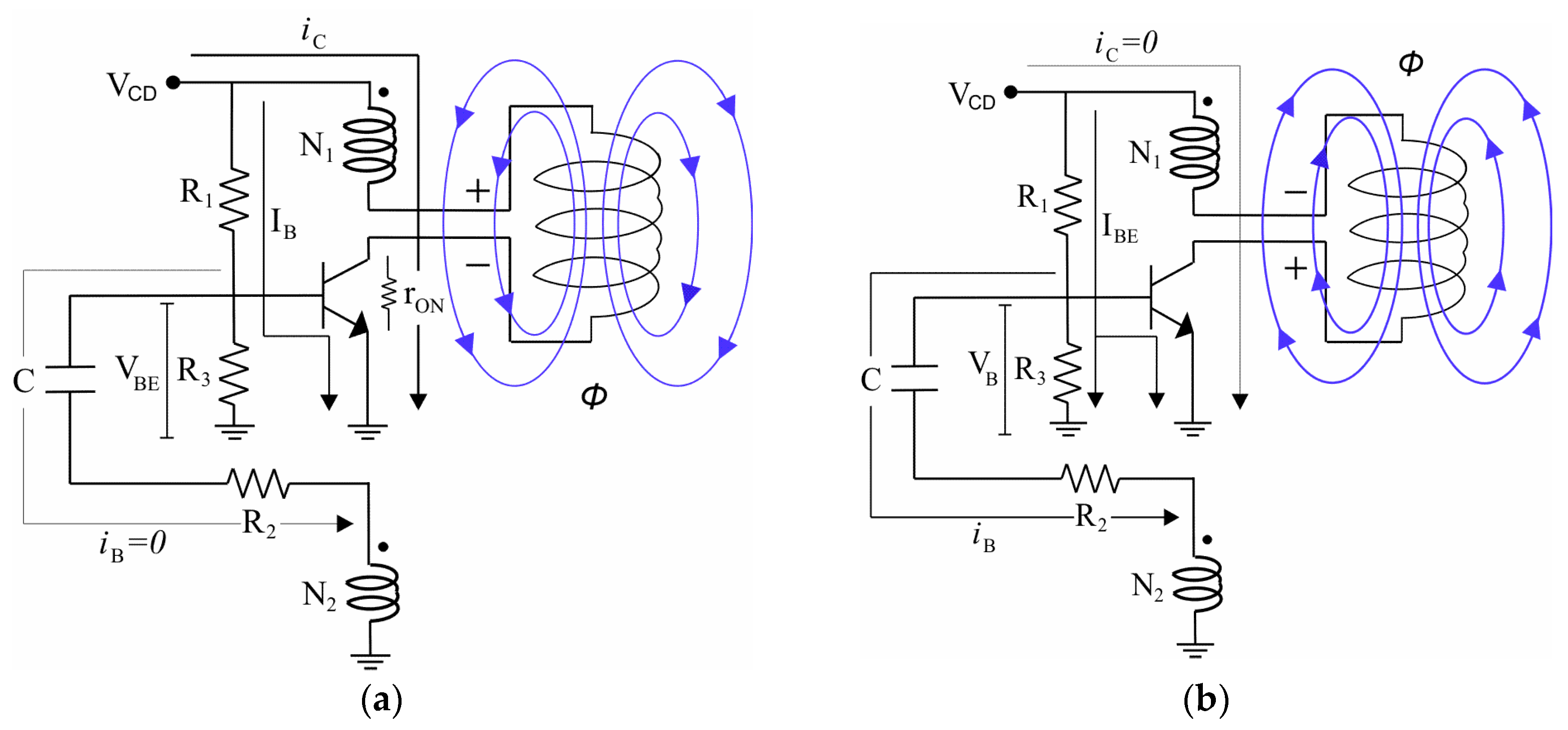
Figure 2a shows the transient current paths and potentials involved during mode 1. The startup operation occurs when the base–emitter junction is biased with a base-to-emitter voltage, V B E , such that the bipolar transistor (BT) becomes quasi-saturated, while the instantaneous collector current, i C , builds up in both the induction coil, L H , and primary inductance, L 1 , in the transformer. The magnetizing energy is stored rapidly, and from L 1 , the primary current is magnetically feedback to the base in direct proportion to the turn ratio ( n = N 1 / N 2 ), with L 2 as secondary inductance. The turn-on time is defined as the time at which the conversion of magnetic energy into heat energy inside the L H is governed by i C upon instantaneous base current i B assumed only by N 1 / N 2 in the transformer. Accordingly, the equations governing the response in mode 1 are
V C D V B E R 1 R 3 + 1 = R 1 I B ,
V C D M   d i B d t = L 1 d i C d t + r O N i C ,
Once i B builds up, a blocking current, I B E , as a trigger current source of sufficient magnitude and width is generated to bring the p-n+ junction diode of the BT at its blocking state with V B as the blocking voltage signal, where at the blocking state, accumulated minority charge carried (electrons) in the base decays exponentially with delay time in absence of a current collector; likewise, bias current becomes very small. The turn-off time is determined when the magnetizing energy stored in both L H and L 1 inductances is dissipated through the collector–emitter junction; then, i B will decrease because the i C magnetically feedback to the base such that the circuit regenerates back into a quasi-saturated state where the BT is back-biased from V C D across the resistor R 1 to recover its stable operating point (mode 1). Figure 2b shows the transient current paths and potentials involved during mode 2. The equation governing the blocking state is
d V B d t + M   d 2 i C d t 2 = L 2 d 2 i B d t 2 R 2 d i B d t C 1 i B ,
As shown in Figure 2, V C D is the voltage used to energize the circuit, V B E is the base-to-emitter ON voltage, r O N is the ON resistance when i C flows through the collector–emitter junction in mode 1, and M = α L 1 L 2 is the mutual inductance between L 1 and L 2 as a function of α , which acts as a coupling coefficient. It is accepted that the circuit operates nonlinearly; thus, magnetic coupling is dependent on a dynamic current gain, β d ~ N E + / N B [7], and ratio i C / i B , which, in turn, change continuously from quasi-saturated states to blocking states. Thus, as the operating states in BT obeys the large-signal transient regime, V B must have sufficient magnitude to ensure a stable turn-off time.

3. Results and Discussion

3.1. Temperature in Induction Coils and Bipolar Transistors

Because the primary purpose of induction heating (IH) is to maximize the heat flux generated on the inner wall of a target material (TM) to be heated, heat-dependent electromagnetic properties must be taken into account when an alternating current (AC) power supply energizes an induction coil, where a magnetic field is formed around it and the TM placed into the magnetic field causes a change in the velocity of the magnetic flux lines. Therefore, the heating depth ( δ H ) is determined by the density of the induced current and concentrated in air gaps to be converted into heat energy, a process dependent on skin depth, defined as δ = π μ 0 σ C f S W 1 , which diminishes when it is flowing closer to the center relative to the inner wall of the induction coil [2]. As the instantaneous AC flowing through the induction coil increases as a function of the operating frequency, the current density around the surface of a TM also intensifies accordingly.
It is well-known that heat transfer through a medium is a three-dimensional phenomenon, where the rate of heat flux through a medium at any point on the surface of any conductive material is perpendicular to that on the surface, as expressed by Fourier’s law of heat conduction, κ T A T , where the temperature gradient, T , is negative because heat diffusion occurs in the positive direction as temperature decreases [8]. Physics analysis to understand how heat distribution operates in a TM dependent on the driving force for heat transfer when the temperature changes can incorporate energy flux from an induction coil at different surface directions if a power equation solved by π 2 r 4 d d B d t describes how the energy flux circulates in air gaps from a circular coil [2,5]. Accordingly, empirical electromagnetic–thermal modeling restricted to simple geometrical features such as flat or nearly curved surfaces can be conducted with sufficient accuracy to learn how the phenomenon of induction heating behaves. An energy balance between heat flux and energy flux when convection and radiation occur simultaneously at the interface between the circular coil and the TM [7] can be expressed as the following time-dependent diffusion equation:
κ T A d T d δ = π 2 r 4 d d B a i r d t ,
Heat transfer can be computed as a one-dimensional phenomenon using Equation (4), with d T = T S T A , d B a i r = B a i r   ×   10 6 , d δ = δ H , d t = f S W 1 = π μ 0 σ C   δ 2 , and δ = 0.05   cm as a reference parameter. Here, A = l H w H is the area of lower curvature in the inner wall of the circular coil, where the heated target adsorbs energy and T S is its resulting surface temperature, with T A = 25   ° C as the initial temperature that corresponds to the ambient temperature, μ 0 = 4 π   ×   10 7   H y m 1 as the permeability of vacuum, σ C = 1   ×   10 7   S m 1 is the electrical conductivity of the copper wires used in circular coils with a single layer of multiple turns, and d = 1.5   ×   10 3   m m 2 is the current density of wires for windings in small switching-mode transformers operating at low power and high frequencies [5].
Due to the junction temperature, T J , inside an NPN power bipolar transistor is dissipated in the form of heat and can be significantly greater than the ambient temperature, semiconductor parameters such as the diffusion coefficient, D n , for the minority charge carriers (electrons) in the base region; the impurity density of an acceptor, N B , in the base region; and its widening, W S C , as space charge toward the collector region can be sensitive to significant increases in temperature [7]. Then, the heat transferred via conduction, radiation, and convection mechanisms must be removed in the NPN power bipolar transistor using an adequate heat sink structure manufactured from aluminum alloy 6063 to absorb heat and limit the rise in their package temperature (case temperature, T C ) caused by thermal conduction and transfer it away to the surrounding atmosphere [9].
Since power dissipation is dependent on several power loss mechanisms, when the transient T J is significantly different from its average value, only switching losses,   P S W = 0.5 V S W I O N f S W ( t R + t F ) and conduction losses,   P D = D r O N I O N 2 are dominant mechanisms under a switching regime [10]. Due to the low-impurity density of donor N C in the collector region, charge accumulation inside the collector region stimulates space-charge-limited conduction (SCLC), which results in an increase in base width, W B , from W B to ( W B + W C ) / 2 in NPN power bipolar transistors, with W C , the collector’s width, being larger than the emitter’s width,   W E [7,11]. In addition, two limitations on power management in modern NPN power bipolar transistors are enabled: thermal runaway and avalanche breakdown. Both events occur at higher temperatures and in turn raise the base and collector currents, with T C increasing to 150 °C or more during conduction and W S C growing considerably.
Due to the average T J under transient operation, the NPN power bipolar transistor can rise with rapid temperature changes, causing fatigue and eventual failure after a finite number of thermal cycles; thus, the V B signal injected in the p-n+ junction diode must have a shorter turn-off time, t O F F , to set a blocking state in the circuit of Figure 2 [5]. Therefore, to evaluate power losses under high-frequency switching, the concept of thermal impedance, defined as Z ( t O N , D ) = r ( t O N ) R θ ( J C ) , is pertinent [10] to analyze how average T J changes in the presence of switching states can be calculated with
T J T A Z t O N , D = P D + P S W ,

3.2. Blocking State Dependence of Design Strategy

A more exact comprehension of the blocking state in Figure 2 can be developed; however, some conditions must be taken into account. From the principle of operation described in Section 2, for the blocking state phenomenon to be nonlinear in nature, V B must be larger than V B E in magnitude, and I B E > I B , where I B E is dependent on the β d I B E 2 = i B i C condition to ensure reliable quasi-saturated and blocking states. Approximated solutions for Equations (2) and (3) using the well-known analytical method to solve the first- and second-order linear differential equations can be determined with the following initial conditions: (a) under the startup condition, V C D = 0 to ensure circuit passivation, while i B = constant to ensure constant bias current in (2). (b) under the cutoff condition, V B = constant to ensure a blocking state, while i C = 0 to ensure M = 0 in the primary to secondary windings of Equation (3). The solution for i C and i B can be written as follows:
i C ( t ) = I C 1 e x p r O N L 1 t ,
i B t = I B e x p R 2 L 2 t c o s 1 L 2 C t ,
To determine the dynamic response of the V B signal, the relationship between current and voltage in the transformer is deduced from Equation (3) as a function of i C and i B currents, and inductances L 1 , L 2 and M are determined as follows:
V B = M   d i C d t L 2 d i B d t ,
A design strategy based on iterative adjustment of curves and using theoretic physical parameters from commercial NPN power bipolar transistors in which their manufacturer’s datasheet is available is proposed first. To achieve linear response and high current gain in the bipolar transistor in Figure 2, the resistor R 1 can be estimated from Ohm’s law (( V C D V B E ) I B 1 ), with β = 100 and V C D chosen from the safe-operating-area (SOA) curve at a forward bias of I C   ~ 1000   m A , while R 2 < R 1 because V B > V B E during the blocking state. According to the ON characteristics declared in datasheets for silicon-based NPN power bipolar transistors available in the market, physical parameters such as maximum I C   ~ 5   A and I B   ~ 0.5   A , as well as r O N   ~ 2   Ω , which is dependent on V B E   ~ 1.2   V and obtained from the SOA curve ( V C D = 40   V ) to operate at I C   ~ 1000   m A , are general purpose values for high-speed applications. Then, theoretic curves for I B E and V B can be searched using reference parameters, such as R 1 < 100   k Ω , R 2 < 10   k Ω , C < 10   n F , and n > 1, to operate the coreless transformer at switching frequencies lower than 500 kHz, in accordance with the n 2 = L 1 / L 2 condition [4,12]. To iteratively adjust β d I B E 2 = i B i C , Equations (6) and (7) are used, where L 1 < 500   μ H and L 2 < 50   μ H are the initial parameters used to obtain an optimal solution when I B E > I B .
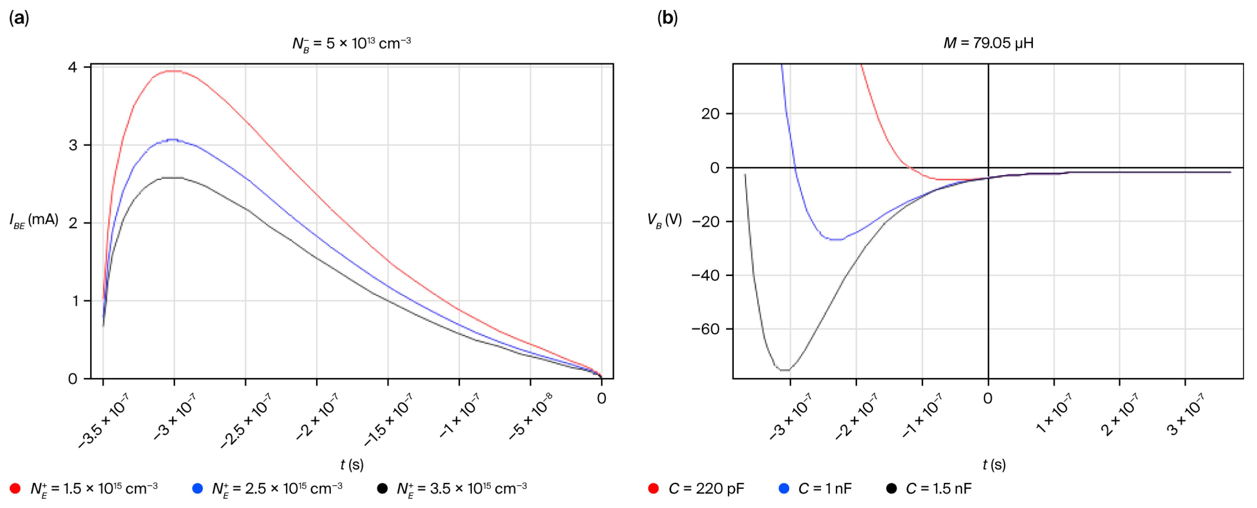
Figure 3a shows how I B E behaves in relation to β d at different values of ionized impurity densities; N E + is in the emitter region, and N B = 5   ×   10 13   c m 3 represents the effective ionized impurity density in the base region [7]. It can be seen that as N E + increases, the magnitude of I B E becomes smaller. Using Equation (8), the variation in the V B signal, shown in Figure 3b indicates that when the coupling capacitor, C , decreases in value and M   ~ 80   μ H with α = 0.5 for high-frequency coreless transformers, the magnitude of V B reduces [13]. It is observed that C 1   n F must be chosen to ensure that V B has an acceptable magnitude in comparison with the maximum base-to-emitter voltage declared on the manufacture’s datasheet.
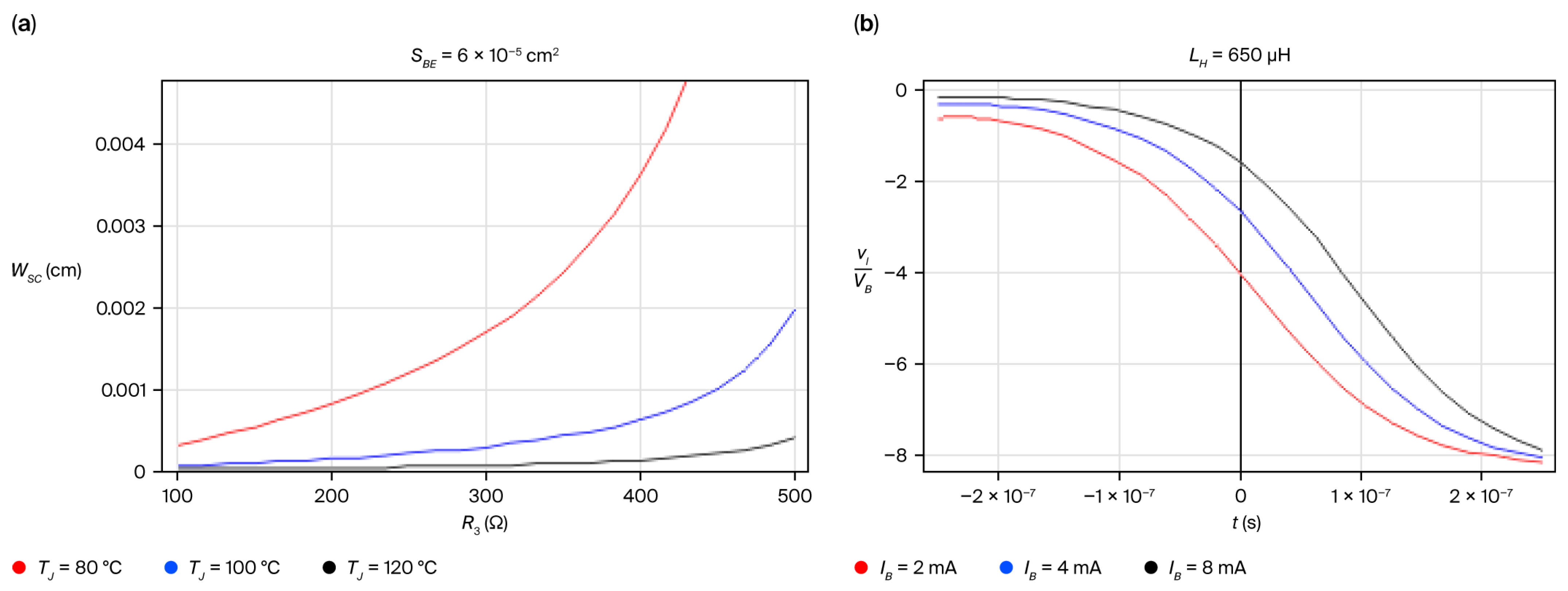
To clarify how the external R 3 parallel-connected in the base–emitter junction is capable of adjusting the heat transfer from the magnetizing energy in the induction coil, it is show that SCLC in the p-n+ junction diode built into the base–emitter junction obeys I B ~ S B E D n n i 2 ( W S C N B ) 1 e q V B E k T 1 as the base current. Thus, Equation (1) is used to solve the theoretic curves shown in Figure 4a. Furthermore, since the injected majority-carrier density inside the base region from the emitter region is extended, space-charge widening, W S C , toward the collector region also increases, which, in turn, causes abrupt changes in conductivity through the collector–emitter junction to decrease and β , where I C = β I B , to descend when the blocking circuit is transiently triggered from the regenerative point to the quasi-saturated operating point as the junction temperature, T J , is raised.
From Figure 4a, it is clear that when R 3 increases, W S C also increases nonlinearly; however, if the T J in the p-n+ junction diode rises to 120   ° C or more, W S C quickly decreases, which means that the NPN power bipolar transistor is prone to damage caused by thermal runaway. In contrast, to cause the bipolar transistor to impart stable energy, T J must be lower than 80   ° C to ensure that W S C can increase gradually as a function of adjustment in R 3 . Curves in Figure 4a were solved by iteratively adjusting Equation (1), with k = 8.62 × 10⁵ eVK1 as the Boltzmann constant; T = TJ + 273.15 in degrees Kelvin, where T J is shown in degrees Celsius; S B E = 6   × 10 5   c m 2 represents the cross-section area for mobile carries across the base–emitter junction; and n i = 1.45   × 10 10   c m 3 is the intrinsic carrier concentration of silicon at room temperature [7].
Because i C is shared between L H and L 1 through the bipolar transistor, as shown in Figure 2, it is important to learn how instantaneous induction voltage, v I = L H d i c d t , and the V B signal are interrelated to properly operate a blocking state with the coreless transformer chosen, as there must be a voltage conversion ratio, v I / V B , that operates as a function of different values of the bias current, I B . Similarly, to ensure magnetizing energy balance between L H and L 1 and to preserve power consumption, it must be taken into account that L H > L 1 is a design condition. It can be observed from Figure 4b that when I B is lower, the energy transferred toward L H change from the blocking state to the quasi-saturated state.

3.3. Experimental Results

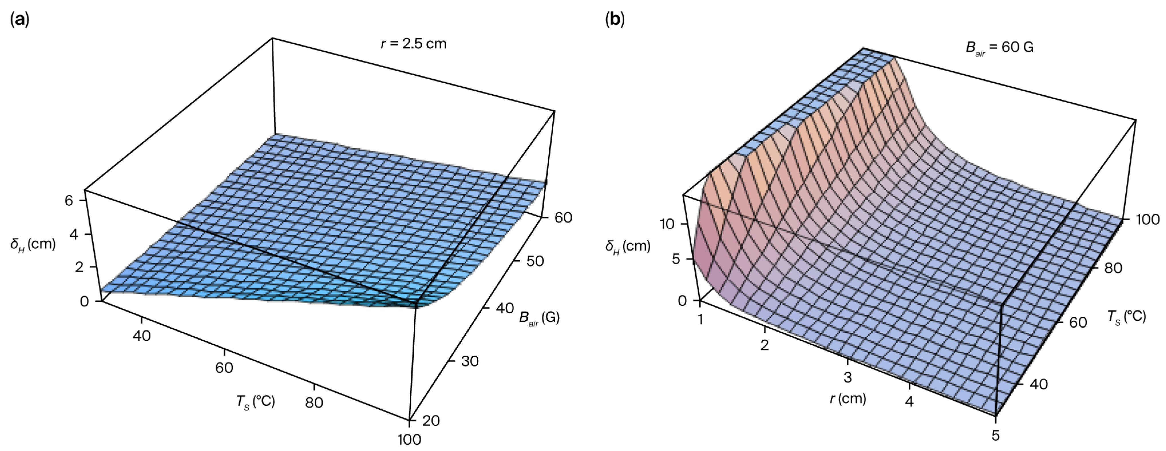
Due to the existence of single-layer coreless circular coils with multiple turns and inductance values lower than 1   m H , induction coils can be manufactured on molds with radii lower than 10 cm; a low-grade ferrous (Fe-FeSn2-Sn) composite that consists of 0.1 wt% carbon–iron sheets coated with a thin layer of tin, commonly used as an internally lacquered food and beverage packaging with low-level toxicity for canned food [10,14,15], which is classified as a nearly linear material with average thermal conductivity, where   κ T = 80   W m 1 K 1 [8], was chosen as the target material (TM); it has a radius of 2 cm, a length of 5 cm, and inner-wall dimensions of length l H = 5   ×   10 2   m and width w H = 2.5   ×   10 2   m , representing the heating region. To determine how heating depth, δ H , behaves, 3D curves describing two scenarios were plotted using Equation (4).
Figure 5a describes how δ H changes when the radius in the induction coil is constant (r = 2.5 cm), while the surface temperature, T S , and B a i r increase from 30 °C to 100 °C and from 20 G to 60 G, respectively. For circular induction coils with radius r ranging from 1 cm to 5 cm and surface temperature, T S , increasing from 30 °C to 100 °C, Figure 5b reveals how the heat distribution occurs when magnetic flux density is constant ( B a i r = 60   G ).
To calculate the temperature ratings in the bipolar transistor when short time pulses of high-voltage flow through the collector–emitter junction and high-frequency currents lower than 1000 mA activate a blocking state, the commercial NPN Silicon Power Transistor (type MJE13005G; ON Semiconductor) was used for predictive analysis. The principle of operation described in Section 2 defines how inductive load is connected to the collector in the bipolar transistor, according to the manufacturers’ datasheet for the MJE13005G device; it specifies that the duty cycle for the V B signal must be D = 0.25 with a rise time t R = 220   n s and a fall time t F = 550   n s . Additionally, the transient thermal impedance factor, r ( t O N ) = 0.2 , is a function of the turn-off time, while junction-case thermal resistance is R O N ( J C ) = 1.67   ° C / W .
To achieve a stable blocking state and a safe thermal cycle, the ratings in junction temperature, T J , were computed using the physical parameters of the MJE13005G device at room temperature (Table 2), which were extracted from the manufacturers’ datasheet and estimated from the literature [7]. Since both space-charge capacitance and the diffusion of charge carries through the base–collector junction are responsible for thermal effects, the switching losses, P S W , in Equation (5) must be dependent on transit-time effects τ t = W S C 2 2 D n ~ f S W 1 , where f S W is the switching frequency [16].
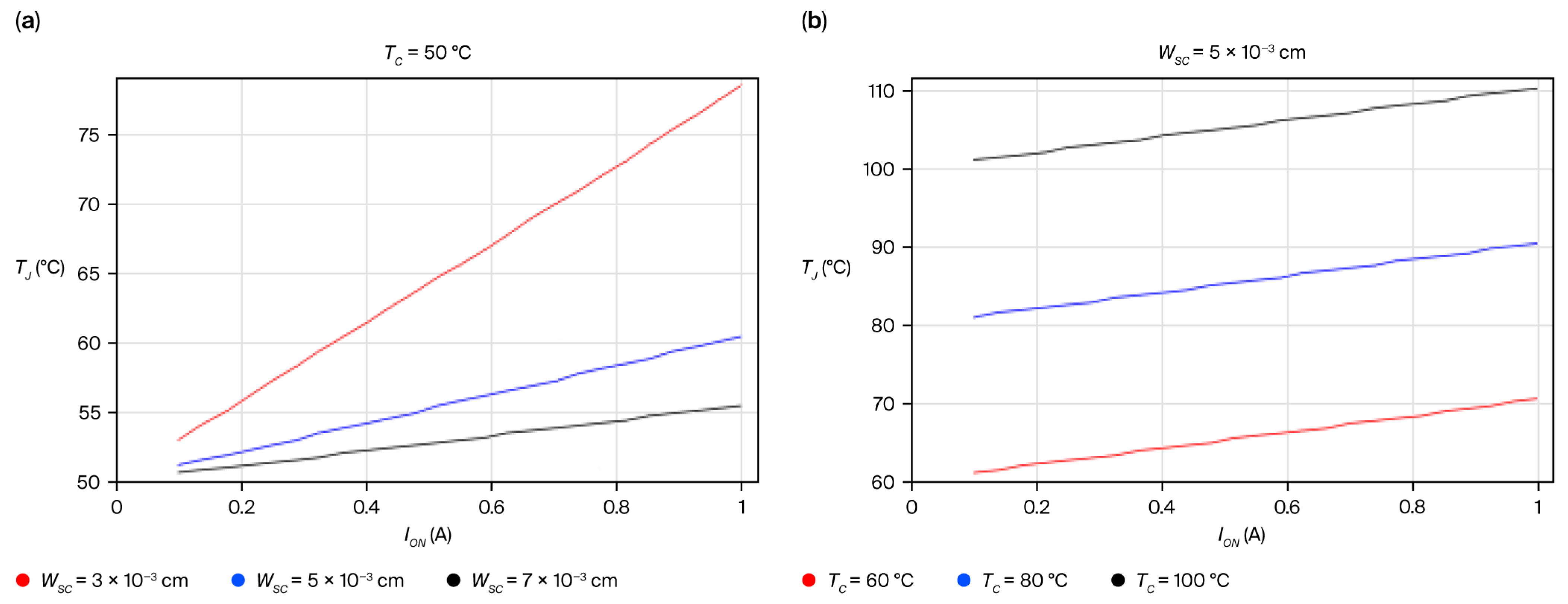
Figure 6 shows how T J changes as a function of the ON current, with I O N ranging from 100 mA to 1000 mA under two conditions: (a) T J is dependent on three different values of space-charge widening, W S C , as shown in Figure 6a, assuming the maximum case temperature T C = 50   ° C in the MJE13005G device with TO-220 package [16]. (b) As shown in Figure 6b, T J changes according to the three examined T C values to generate a quasi-saturated state at lower W S C = 5   ×   10 3   c m , where majority-carrier density in the base region is moved from the emitter region. Therefore, it can be specified that the acceptable I O N to operate the blocking circuit must be lower than 500 mA to trigger the energy threshold to permit a rapid build-up of regeneration in response to reduces T J and shrinks W S C , which means that a medium electron density at the base–collector junction approaches the majority-carrier density in the collector region. According to Figure 3, as N E + grows in the emitter region, the W S C is expected to shrink, which results in a smaller magnitude of the V B signal to ensure reduced minority-carrier injection from the collector region toward the base region in response to the action of the coupling capacitor, C , together with the resistor, R 3 , in the circuit of Figure 2.
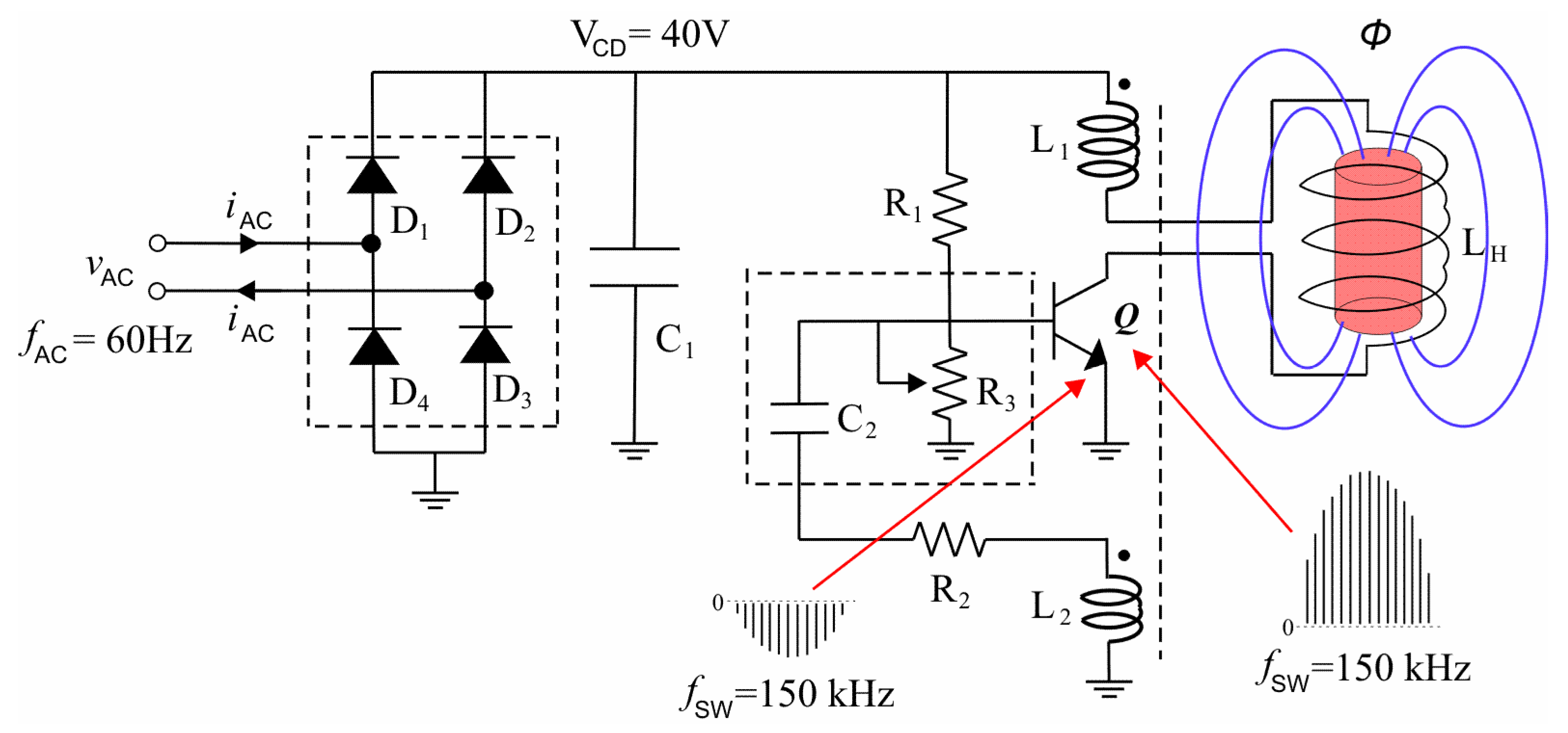
A prototype circuit was built, and measurements were taken in order to validate the earlier physics-based analytical model. To practically implement and verify the proposed blocking circuit built with the commercial NPN Silicon Power Transistor from ON Semiconductor (with part number MJE13005G), a full-bridge rectifier and an input filter capacitor operating at a voltage of V A C = 84.5   V (peak magnitude) from the low-frequency AC power supply were used, as shown in the diagram in Figure 7, to energize it, with average T J lower than 80   ° C when short time pulses at high-frequency in both the base–emitter junction and the collector–emitter junction are switching.
The practical components used in the prototype are listed in Table 3. Both the induction coil and the coreless transformer were designed using a previous method of designing coreless magnetic devices [4,13]. All the waveforms recorded were measured using a digital storage oscilloscope (Tektronix (Beaverton, OR, USA), TDS1012C 100 MHz). The temperature measurement in both the MJE130005G device and the TM to be heated by induction was performed using the precision integrated-circuit temperature sensor (type LM35DZ; Texas Instruments (Kuala Lumpur, Malaysia)) packaged in TO-92 plastic and designed for a full range from −55 °C to 150 °C [17].
In accordance with the T J dependence in Figure 6, heat transfer from the in the TO-220 package of the MJE13005G device toward the surrounding atmosphere has values of T C lower than 80   ° C and T J not exceeding 120   ° C ; a conventional heat sink with fins [5,9], commonly used in power electronics with a surface area of 50 × 30 mm2 and a thickness of 2 mm, where nine fins are equally spaced 5 mm apart with 10 mm of height and a thickness of 1 mm between each one, was chosen as the heat sink structure when the MJE13005G device was mounted on it in absence of silicone grease.
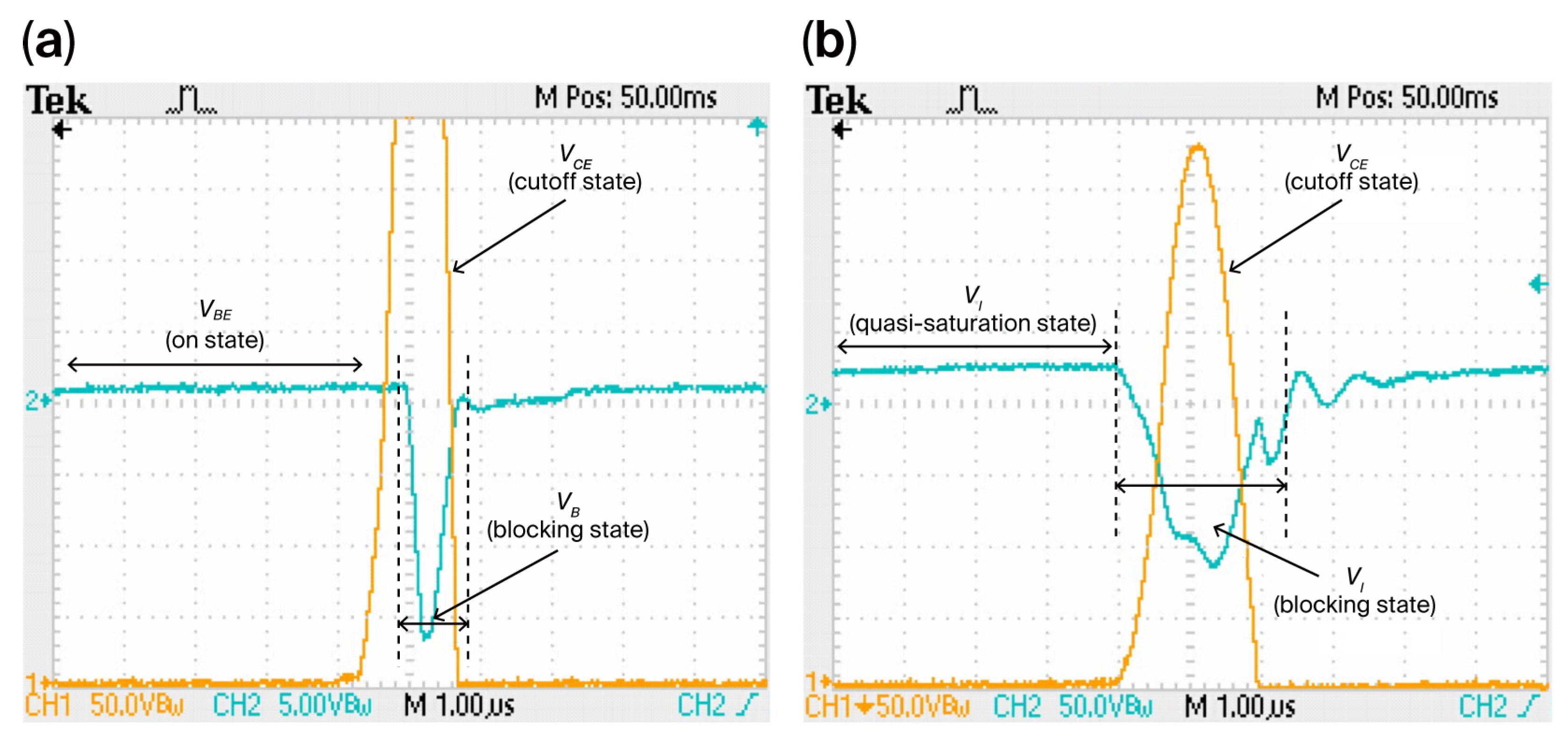
To analyze the dynamic behavior in the blocking circuit, the chosen TM was placed inside of an induction coil to evaluate the heating phenomena, as shown in Figure 7, with typical waveforms from the prototype operating under maximum heating conditions shown in Figure 8. The input V B signal in the base–emitter junction and the output V C E signal at the collector–emitter junction are shown in Figure 8a, which also depicts the operating states: the on-state voltage V B E = 1.2   V in the p-n+ junction diode, the blocking state with V B = 18.2   V (peak magnitude) as the blocking voltage, and V C E = 800   V (peak magnitude) during the cutoff state in the MJE13005G device. Figure 8b reveals that a high-speed transition between the quasi-saturated state with a magnitude of V I = 72   V and a blocking state with a magnitude of V I = 146   V defines an induction voltage, v I = L H d i c d t , corresponding to an oscillating signal responsible for the magnetizing cycle during turn-on time and the demagnetizing cycle during turn-off time. It was observed that such a v I signal resulted in an asymmetrical curve in comparison with the symmetrical sinusoid signals generated in half-bridge series resonant circuits [1]. The v I signal is responsible for the fast change from the quasi-saturated state to the blocking state during the induction heating process.
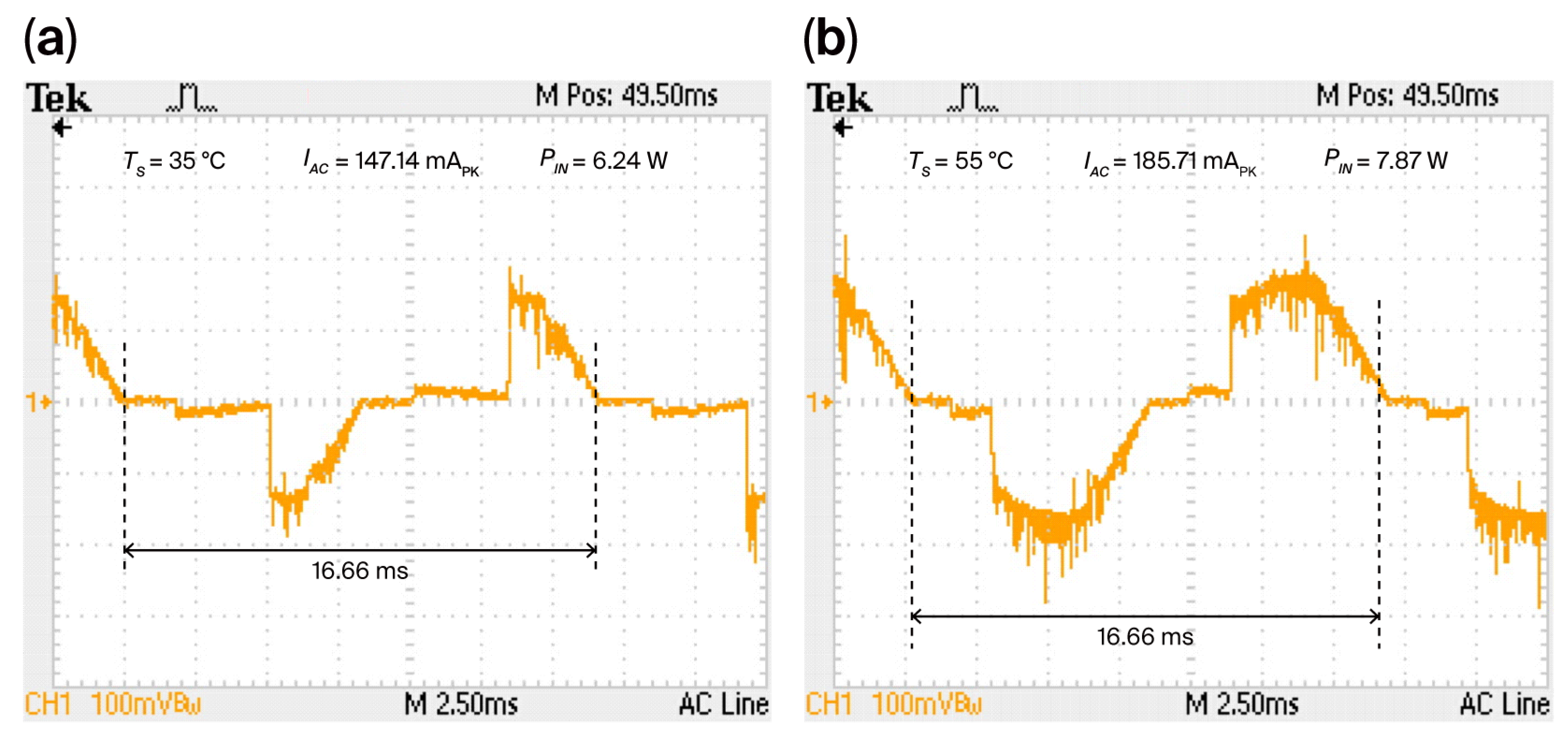
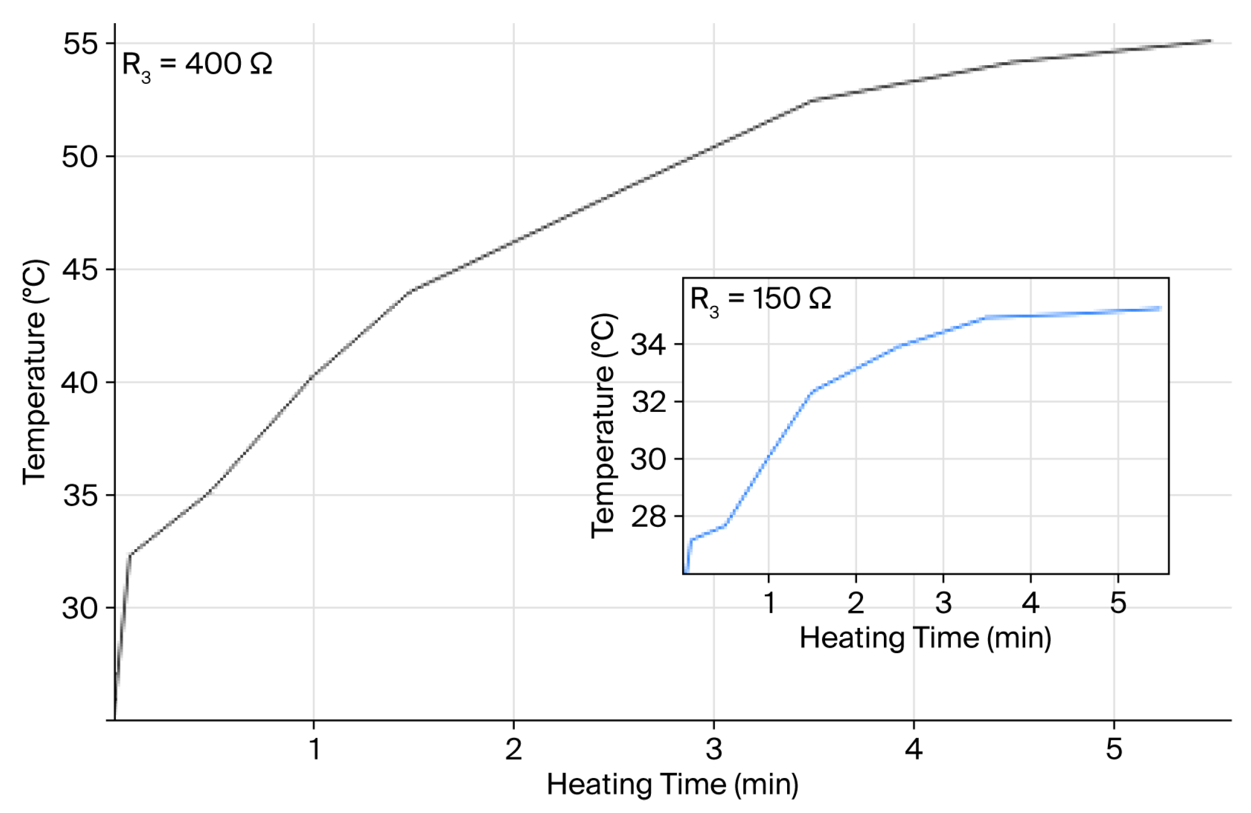
Taking R3 as a parameter, two waveforms of the alternating current (AC) signal were registered. To validate the predictive operating range from Figure 4a, the magnitude of the AC, I A C , was specified when R 3 was fixed at a lower value of 150 Ω, as shown in Figure 9a, and a higher value of 400 Ω, as shown in Figure 9b. When the LM35DZ sensor was placed inside the TM, the maximum T S was also registered during the induction heating process. Temperature evolution was also observed over 5 min, as depicted in Figure 10, where a gradual change in temperature from 25 °C as the initial value to 60 °C as the final value on the inner wall of the TM was done in two scenarios: when R 3 was adjusted to 150   Ω and when R 3 was adjusted to 400   Ω . However, when the LM35DZ sensor was placed on the fins of the heat sink structure, a linear increase was observed in temperature from 60 °C to 70 °C, which means that the MJE13005G device was thermally stabilized.
By applying standard deviation analysis to the curves in Figure 10, fluctuations in temperature can be calculated using σ = 1 N n = 1 N T n T a v g 2 , where N is the total number of values to be evaluated from the curves. When R 3 = 150   Ω and T a v g = 35   ° C are expected, the deviation was σ   ~ 4.2   ° C . However, a deviation of σ   ~ 9.45   ° C is achieved when R 3 = 400   Ω and T a v g = 50   ° C . The temperature–time curves show that instantaneous heat dissipation will occur as a function of the heating time, and the gradual change in temperature observed in Figure 10 confirms that the magnetic hysteresis phenomenon is also responsible for the heating process [4,18].
It can be observed from Figure 8 that the measured switching frequency was 150   k H z , where the time width for the V B signal during the blocking state resulted yielded 0.8   μ s , while that during the quasi-saturated state yielded 4   μ s . In comparison, the theoretic times during the blocking state was ~ 0.35   μ s and during the quasi-saturated state was ~ 1.5   μ s , as shown in Figure 3 with switching frequency of ~ 500   k H z . A dynamic temperature change inside the base region in the MJE13005G device is sensitive to causes practical ON-resistance to be higher than r O N as declared in Table 2 for iterative adjustment of curves, and significant delay time by accumulated minority charge carriers [7]. A time deviation was observed in the switching times among the predicted values and those measured values, which indicates that predictive capability from the iterative adjustment of curves is only useful as initial design guidance, but if practical r O N > 2.5   Ω and delay time ~ 0.1   μ s for MJE13005G device are taken into account in Equations (6) and (8), a closer predictive capability can be succeeded. In agreement with Figure 6, there are errors less than 10 °C for the temperature range from 60 °C to 70 °C, as measured in the heat sink structure, when I O N is lower than 200 mA, which shows that accuracy in the temperature analysis is pertinent as the first design criteria.
Because the amount of stored energy ( 0.5 I A C 2 L ) in both the inductor coil and the primary inductance of the transformer is dependent on the quasi-saturated state at 4   μ s , as shown in Figure 8, 0.5 I A C 2 L significantly grows as a function of the AC power supply at a line frequency of 60 Hz, but it is quickly dissipated in a short time span of 0.35   μ s thanks to the action of the coupling capacitor, C , together with a resistor,   R 3 . Therefore, in accordance with the inductive switching curves from the manufacture’s datasheet for the MJE13005G device, if I C is lower than 10 mA and I B = 0 under OFF characteristics with T C lower than 80   ° C , the voltage margin for V C E during blocking state in time interval of 2   μ s in open circuit can be only 15% more than V S W   ~ 700   V (maximum collector-to-emitter voltage). The safe operating limit for MJE13005G device under repetitive maximum V C E   ~ 800   V pulses can be securely by the discontinuous conduction mode, which occur before to startup operation of the blocking circuit at two time intervals in the I A C signal, as shown in Figure 9, characterized when magnitude of I A C achieves zero while V B < 9   V , and by the heat sink structure chosen to preserve the package temperature ranging from 60 °C to 70 °C, when the V C E signal was modulated by the AC power supply at a line frequency of 60 Hz, as shown in Figure 7. As result, average V C E signal helped to compensate the temperature rise during each 16.6 ms, which explains why the blocking circuit performs securely over 5 min, as shown in Figure 10.
The conversion of heat energy from magnetizing energy can be validated with an overall energy balance analysis, where an average output power, P O U T   ~ 0.5 V I I A C , yielded ~ 5 W in comparison with the input power, P I N   ~ 0.5 V A C I A C , specified in Figure 9. Thus, approximated efficiency decreased from 80% to 60% when the magnitude of I A C increased, which means that power loss variations in the building blocks of the proposed blocking circuit in Figure 7 are significant. Using definitions of P d i o d e = 2 V D I A C (half-bridge rectifier per cycle with V D   ~ 0.75   V ), both P D = D r O N I O N 2 (conduction losses) and P S W = 0.5 V S W I O N f S W ( t R + t F ) (switching losses), with I A C ~ I O N measured from Figure 9; power losses per cycle in the full-bridge rectifier yielded P d i o d e   ~ 0.25   W , while those in the MJE13005G device yielded P D   ~ 0.05   W and P S W   ~ 0.1   W . From Figure 8 and Figure 9, the equivalent average resistor ( R H = V I I A C   ~ 438.54   Ω ) for the induction coil was estimated; then, average power losses were defined as P H = 0.5 I A C 2 R H f S W τ , and the time constant was determined to be τ =   L H R H   ~ 1.35   μ s , yielding P H   ~ 1.5   W , which is comparable to that of the primary inductance in the transformer. Total power losses, P d i o d e +   P D + P S W + P H , were lower than those estimated using P O U T , which specifies that the energy transfer toward the induction coil using the blocking circuit is somewhat limited.
The benefits of the proposed converter based on the blocking state in a bipolar transistor are the absence of a driver and easy adjustment of local temperatures (using only an external variable resistor) in a magnetic heating medium. Thus, the magnetic hysteresis phenomenon, as the dominant heating principle, proves that the prototype analyzed here is a suitable alternative for a medical treatment device where in vivo clinical trials perform heating for less than 10 min [4]. Furthermore, it is possible to diminish the power losses (switching times) at rated conditions with Al-GaN/GaN-based NPN power transistors by enhancing physical parameters, such as the breakdown field and current density, while reducing the specific ON resistance to operate over a wide input and output voltage range [19,20].

4. Conclusions

In this study, physics-based analytical models and operational characteristics were introduced for the conversion of magnetizing energy into heat using the blocking state in a NPN Silicon Power Bipolar Transistor. In spite of using only one power switch for low-power applications, the proposed blocking circuit can preserve the advantages of converting likewise to the conventional half-bridge series resonant circuits; however, due to the change in efficiency, limited voltage margin for heating times higher than 5 min, and the latent increase in power losses, it is recommend using a NPN Silicon Power Bipolar Transistor in the TO-247 package with V S W   ~ 1000   V and I C   ~ 5000   m A for more reliable operation.
The operation principle, theoretic analysis, and experimental evaluation were taken from a laboratory prototype. According to the theoretic analysis, it was shown that the blocking state in a bipolar transistor can be used for the heating of low-grade ferrous composites via magnetic induction. The novel advantages of the proposed circuit over heat energy conversion are as follows: the temperature in the heated target can be adjusted in the absence of an extra driver circuit. Additionally, commercial NPN Silicon Power Transistors available for educational practice can be used, and further research can be conducted using Al-GaN/GaN-based heterojunction bipolar transistors (HBTs).

Funding

This research received no external funding, and the APC was funded by the author.

Data Availability Statement

All of the data are available in the manuscript. Ultimately, the intention of the author is to encourage scholars to explore new empirical research routes using similar methodologies to those documented here.

Acknowledgments

The experiments were made possible thanks to the assistance provided by the technical personnel of the Electronics Laboratory, Instituto Politécnico Nacional-ESIME Zacatenco, México City.

Conflicts of Interest

The author declares no conflicts of interest.

References

  1. Lucia, O.; Maussion, P.; Dede, E.J.; Burdio, J. Induction Heating Technology and Its Applications: Past Developments, Current Technology, and Future Challenges. IEEE Trans. Ind. Electron. 2013, 61, 2509–2520. [Google Scholar] [CrossRef] [Scilit]
  2. Areitioaurtena, M.; Segurajauregi, U.; Akujärvi, V.; Fisk, M.; Iker Urresti, I.; Ukar, E. A semi-analytical coupled simulation approach for induction heating. Adv. Model. Simul. Eng. Sci. 2021, 8, 14. [Google Scholar] [CrossRef] [Scilit]
  3. Hirata, A.; Onishi, T.; Shinohara, N.; De Santis, V.; Diao, Y.; Feliziani, M.; Hikage, T.; Lan, J.; Maradei, F.; Miwa, K.; et al. Electromagnetic Field Exposure Assessment and Mitigation Strategies for Wireless Power Transfer Systems: A Review and Future Perspectives. IEEE J. Wirel. Power Technol. 2026, 1, 0800119. [Google Scholar] [CrossRef] [Scilit]
  4. Zhang, Y.F.; Lu, M. Advances in magnetic induction hyperthermia. Front. Bioeng. Biotechnol. 2024, 12, 1432189. [Google Scholar] [CrossRef] [Scilit] [PubMed]
  5. Chryssis, G. High-Frequency Switching Power Supplies: Theory and Design, 2nd ed.; McGraw-Hill Publishing Company: Columbus, OH, USA, 1989; pp. 41–45, 109–133. [Google Scholar]
  6. Rashid, M.H. Power Electronics: Devices, Circuits, and Applications, 4th ed.; Pearson Education: Courier Westford, MA, USA, 2014; pp. 385–395, 931–941. [Google Scholar]
  7. Sze, M.S.; Ng, K.K. Physics of Semiconductor Devices, 3rd ed.; John Wiley & Sons, Inc.: New York, NY, USA, 2007; pp. 54–56, 62–69, 244–258. [Google Scholar]
  8. Zemansky, M.W. Heat and Thermodynamics, 5th ed.; McGraw-Hill Book Company: Columbus, OH, USA, 1968; pp. 91–103. [Google Scholar]
  9. Habib, N.; Siddiqi, M.U.R.; Tahir, M. Thermal Analysis of Proposed Heat Sink Design under Natural Convection for the Thermal Management of Electronics. Therm. Sci. 2022, 26, 1487–1501. [Google Scholar] [CrossRef] [Scilit]
  10. Andresen, M.; Liserre, M. Impact of active thermal management on power electronics design. Microelectron. Reliab. 2014, 54, 1935–1939. [Google Scholar] [CrossRef] [Scilit]
  11. Baliga, B.J. Modern Power Devices, 2nd ed.; John Wiley & Sons, Inc.: New York, NY, USA, 1992; pp. 344–380. [Google Scholar]
  12. Sedra, A.S.; Smith, K.C. Microelectronics Circuits, 5th ed.; Oxford University Press Inc.: New York, NY, USA, 2004; pp. 946–956. [Google Scholar]
  13. Chen, M.; Araghchini, M.; Afridi, K.-K.; Lang, J.-H.; Sullian, C.-R.; Perreault, D.-J. A Systematic Approach to Modeling Impedances and Current Distribution in Planar Magnetics. IEEE Trans. Power Electron. 2016, 31, 560–580. [Google Scholar] [CrossRef] [Scilit]
  14. Blunden, S.; Wallace, T. Tin in canned food: A review and understanding of occurrence and effect. Food Chem. Toxicol. 2003, 41, 1651–1662. [Google Scholar] [CrossRef] [Scilit] [PubMed]
  15. Haftek, E.; Tan, M.; Barnard, J.A. Microstructure and magnetic properties of ferromagnetic Fe-Sn alloy thin films. Ultramicroscopy 1992, 47, 400–407. [Google Scholar] [CrossRef] [Scilit]
  16. Baca Arroyo, R. Unusual Operation of the Junction Transistor Based on Dynamical Behavior of Impurities. Adv. Condens. Matter Phys. 2018, 2018, 4237686. [Google Scholar] [CrossRef] [Scilit]
  17. Baca-Arroyo, R. Effects of Switching on the 2-DEG Channel in Commercial E-Mode GaN-on-Si HEMT. Micromachines 2025, 16, 1173. [Google Scholar] [CrossRef] [Scilit] [PubMed]
  18. Guo, P.; Huang, W.; Feng, X.; Zhang, Z.; Liu, Y. Hysteresis measurement and generic modeling of magnetostrictive materials under high-frequency excitation and high-intensity bias field. Measurement 2024, 228, 114385. [Google Scholar] [CrossRef] [Scilit]
  19. Joishi, C.; Rahman, S.I.; Rajan, S. Tunnel Junction-enabled AlGaN/GaN Heterojunction Bipolar Transistors with all n-type Contacts. IEEE Trans. Electron Devices 2024, 71, 6460–6464. [Google Scholar] [CrossRef] [Scilit]
  20. Zhang, L.; Wang, X.; Zeng, J.; Jia, L.; Cheng, Z.; Ai, Y.; Liu, Z.; Tan, W.; Zhang, Y. AlGaN/GaN Heterojunction Bipolar Transistors with High Current Gain and Low Specific ON-Resistance. IEEE Trans. Electron Devices 2022, 69, 6333–6336. [Google Scholar] [CrossRef] [Scilit]
Figure 1. (a) Conventional blocking circuit; (b) proposed blocking circuit for IH application.
Electronics 15 04022 g001
Figure 2. Operation of the proposed blocking circuit: (a) turn-on time in mode 1; (b) turn-off time in mode 2.
Electronics 15 04022 g002
Figure 3. Blocking state in a bipolar transistor: (a) blocking current signal dependent on ionized impurity density; (b) blocking voltage signal dependent on the coupling capacitor.
Electronics 15 04022 g003
Figure 4. (a) Action of R 3 as a function of the SCLC dependent on junction temperature; (b) voltage conversion ratio dependent on the base current.
Electronics 15 04022 g004
Figure 5. Distribution of heat energy inside the TM in relation to the surface temperature: (a) the radius of the induction coil is constant, while B a i r is variable; (b) B a i r is constant, while the radius of the induction coil is variable.
Electronics 15 04022 g005
Figure 6. Junction temperature in response to the ON current of the MJE13005G device: (a) change in space-charge widening with T C constant; (b) change in junction temperature in the TO-220 package with W S C constant.
Electronics 15 04022 g006
Figure 7. Schematic of the proposed blocking circuit with extra circuits to average T J in the commercial MJE13005G device for induction heating applications.
Electronics 15 04022 g007
Figure 8. Experimental waveforms from the base–emitter and collector–emitter junctions of the MJE13005G device: (a) V B E in the on state, V B in the blocking state, and V C E in the cutoff state; (b) the V I signal in the induction coil in comparison with the V C E signal in the cutoff state.
Electronics 15 04022 g008
Figure 9. Experimental waveforms of the input current i A C signals: (a) R 3 adjusted to 150 Ω; (b) R 3 adjusted to 400 Ω.
Electronics 15 04022 g009
Figure 10. Temperature–time curves to validate the heating kinetics in the TM when magnetic hysteresis phenomenon is enabled by the blocking circuit.
Electronics 15 04022 g010
Table 1. Comparison of the different configuration parameters applied to induction heating [1,4].
ParameterFull-Bridge Series Resonant ConverterHalf-Bridge Series Resonant ConverterZero-Voltage-Switching ConverterProposed Converter
Semiconductor typeIGBTMOSFETMOSFETBT
Switching times<500 ns<100 ns<100 ns<1 µs
Driver technologyCurrent-phase controlPulse-width modulation (PWM)Modern adaptive controlNonexistence
ApplicationIndustrial systems
(150 to 300 °C)
Industrial and domestic systemsDomestic induction cookers (~200 °C)Clinical treatment (Hyperthermia) (~50 °C)
Heating principleEddy currents and magnetic hysteresisEddy currentsEddy currentsMagnetic hysteresis
Operating frequencyLow (<20 kHz)High (>100 kHz)Medium (<100 kHz)High (<400 kHz)
Power lossesMediumLowNegligibleMedium
Table 2. Physical parameters of the commercial MJE130005G device.
SymbolValueSymbolValue
Dn1.41 cm2/sVBE1.2 V
NB~2 × 1017 cm−3VCE0.5 to 1 V
NC~5 × 1014 cm−3rON2.5 Ω
NE~5 × 1019 cm−3IC4 A
WB~10 µmVSW700 V
WC~50 µmβ = hFE8 to 40
WE~30 µmTJ−65 to 150 °C
Table 3. List of components for the prototype circuit.
SymbolComponent Description
D1 to D4Full-bridge rectifier at 1000 mA
C1Polyester, 470 nF/250 V
R1, and R222 kΩ (1/2 W at 5%), and 820 Ω (1 W at 5%)
R3100 Ω to 500 Ω (variable resistor)
C2ESR, ceramic, 1 nF/50 V,
L1550 µH (N1 = 350 turns), 32 AWG wire, and AE = 0.25 cm2
L250 µH (N2 = 25 turns), 32 AWG wire, and AE = 0.25 cm2
LH650 µH (circular coil with single layer of 100 turns),
30 AWG wire, and r = 2.5 cm
QMJE13005G; ON Semiconductor
Disclaimer/Publisher’s Note: The statements, opinions and data contained in all publications are solely those of the individual author(s) and contributor(s) and not of MDPI and/or the editor(s). MDPI and/or the editor(s) disclaim responsibility for any injury to people or property resulting from any ideas, methods, instructions or products referred to in the content.