
Review

Source-Gated Transistors as BEOL-Compatible Devices for Monolithic 3D Integration: Architectures, Materials, and Spatial Validation


School of Electronic and Electrical Engineering, Hongik University, Seoul 04066, Republic of Korea
*
Author to whom correspondence should be addressed.
Electronics 2026, 15(17), 3824; https://doi.org/10.3390/electronics15173824
Submission received: 22 July 2026 / Revised: 18 August 2026 / Accepted: 22 August 2026 / Published: 26 August 2026
(This article belongs to the Special Issue Edge-Intelligent Sustainable Cyber-Physical Systems)

Abstract

The semiconductor industry faces converging pressures from energy-constrained edge electronics and energy-bottlenecked high-performance computing, motivating heterogeneous monolithic three-dimensional (M3D) integration as a system-level response. M3D imposes a strict back-end-of-line (BEOL) thermal budget on upper-tier devices, restricting the channel materials and contact processes available and degrading conventional thin-film transistor performance. The source-gated transistor (SGT), in which drain saturation is set by gate-modulated injection across an engineered source barrier rather than by drain-side channel pinch-off, provides a device-level response: low saturation voltage, high output impedance, large intrinsic gain, and tolerance to channel-length variation, all achieved with moderate-mobility and nonideal-contact channel materials. This review organizes reported SGTs by source-barrier architecture and channel-material platform, develops a spatial characterization framework that complements electrical measurements for unambiguous identification of source-controlled operation, and surveys applications across standalone edge electronics and BEOL-compatible upper tiers in M3D stacks. Integrating non-volatile memory mechanisms into the source barrier further extends SGTs into a compute-in-memory and neuromorphic upper-tier role in which the voltage-invariant saturation current itself functions as a programmable, read-bias-robust state variable. Together, these considerations position SGTs as a flexible architectural primitive for heterogeneous M3D platforms that address the energy demands of both edge and high-performance computing.

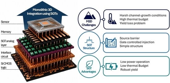
Graphical Abstract

1. Introduction

The semiconductor industry now faces two simultaneous pressures, first of which is the demand for energy-proportional functionality at the network edge: Internet-of-things nodes, wearable and implantable sensors, edge artificial-intelligence accelerators, and distributed control electronics must remain active for long periods under tight energy budgets [1,2,3,4,5]. The second is the demand for energy-efficient throughput in high-performance computing: training and inference workloads at the data-center scale are growing exponentially, while supply-voltage reduction has stalled, leakage currents now dominate a substantial fraction of static chip power, and dark-silicon constraints prevent simultaneous high-frequency operation across all transistors on a die [1,6,7,8,9,10,11,12]. Continued areal scaling alone can no longer reconcile these requirements [6,9,10]. These two pressures are typically treated as distinct engineering problems, yet their architectural responses are converging on the solution.
Heterogeneous M3D integration has emerged as a common response to these challenges. It addresses edge demands by co-locating sensing, amplification, memory, and control in vertically integrated stacks, and it addresses high-performance-computing demands by mitigating the data-movement and memory-bandwidth bottlenecks that limit energy-per-operation in datacenter logic [6,13,14]. Among the available three-dimensional integration approaches, M3D is distinguished by sequential fabrication of upper device tiers on top of a fully processed lower tier [15,16,17], enabling lithographically defined vertical interconnects with pitches well below those achievable by hybrid bonding or microbumping [14,18,19]. Recent demonstrations show that M3D is moving from concept to early prototype [20,21,22], and semiconductor roadmaps now identify heterogeneous M3D as one of the principal pathways “beyond More Moore” [23,24,25].
M3D integration imposes a strict constraint on the transistor fabrication of the upper tiers. Because the BEOL of the lower tier is already complete, subsequent processing must remain within a thermal budget typically near or below 400 °C [13,16,24,26,27]. Conventional single-crystal silicon transistor processes do not satisfy this constraint; upper tiers therefore rely on materials that can be deposited or transferred at low temperature, including amorphous silicon, oxide semiconductors, organic semiconductors, nanowires, and two-dimensional (2D) semiconductors [20,21,28,29,30]. While compatible with BEOL processing, these materials generally exhibit lower carrier mobility, higher trap density, grain-boundary disorder, and less ideal contacts than crystalline silicon [28,29,30,31]. In conventional metal-oxide-semiconductor field-effect transistors (MOSFETs) and standard thin-film transistors (TFTs), where the drain current is dominated by gate-controlled channel conductance and saturation by drain-side pinch-off [32,33,34,35], these material limitations directly degrade transconductance, current saturation, and threshold uniformity.
The source-gated transistor was originally introduced as a low-voltage thin-film device strategy [36], and a substantial body of work has since established its value for display backplanes, flexible analog amplifiers, biosensors, photodetectors, and printed circuit elements. Previous reviews and perspective studies have addressed the electrostatic design principles of contact-controlled transistors [37], unconventional material platforms and applications of SGTs [38], and the broader technological roadmap for Schottky-barrier transistors [39]. The present review is intentionally selective rather than exhaustive and takes a distinct, integration-oriented perspective: we examine how source-barrier architectures, BEOL-compatible material platforms, and spatial validation of source-controlled operation determine the suitability of SGTs as upper-tier devices for M3D integration. The following four observations underline this argument:
  • SGTs accommodate moderate mobility and nonideal contacts of low-temperature, BEOL-compatible channel materials, including amorphous silicon, oxide semiconductors, and two-dimensional materials [40,41].
  • They reach drain saturation at structurally lower voltages than conventional FETs, providing the per-tier power headroom that vertical stacking demands [36].
  • They tolerate channel-length variation, a property especially important for vertically stacked architectures whose overall yield decreases exponentially with the number of tiers [42].
  • They admit multiple source-barrier architectural realizations—Schottky [36,43], tunnel-contact [43,44,45,46,47,48,49], bulk-barrier [50,51,52], and the recently emerging ferroelectric class [53,54,55]—that map onto the heterogeneous functional demands of M3D stacks, from low-power local computation to non-volatile analog-weight elements for neuromorphic acceleration.
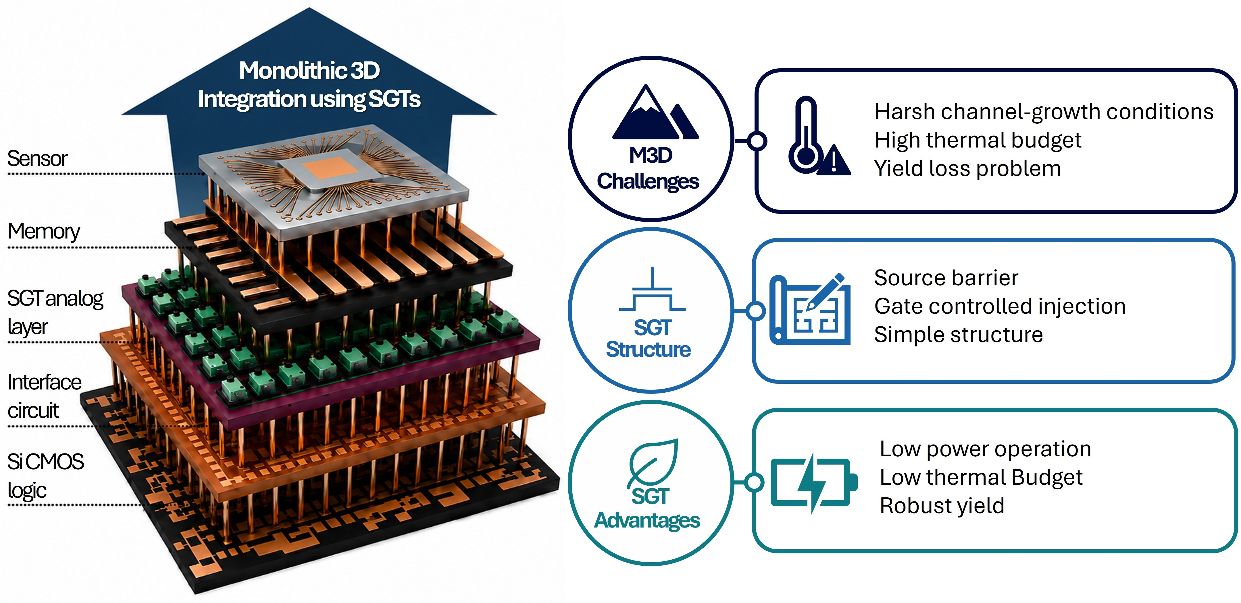
An SGT remains a low-power device at the unit level—it trades peak drive current for early saturation, high output resistance, and material tolerance. At the system level, however, this same trade-off is precisely what makes SGTs viable as upper-tier devices in M3D stacks, and the resulting heterogeneous platform serves both energy-constrained edge nodes and energy-bottlenecked high-performance computers. In the heterogeneous M3D vision developed throughout this review (see Graphic Abstract), high-performance silicon Complementary Metal-Oxide-Semiconductor (CMOS) occupies the front-end-of-line tier, while upper tiers host low-power oxide and 2D SGTs for local computation, sensor readout, and always-on control, as well as ferroelectric SGTs as non-volatile analog-weight elements for compute-in-memory and neuromorphic acceleration [13]. Section 2 summarizes the electrical signatures of SGT operation. Section 3 develops the design space of SGTs, encompassing the physical mechanism, source-barrier architectures, channel-material platforms, and a spatial validation framework for source-controlled operation. Section 4 surveys SGT applications across edge electronics and monolithic 3D integration, with the latter extended to memory-integrated upper tiers for compute-in-memory and neuromorphic acceleration. Section 5 concludes the review.

2. Electrical Signatures of SGT Operation

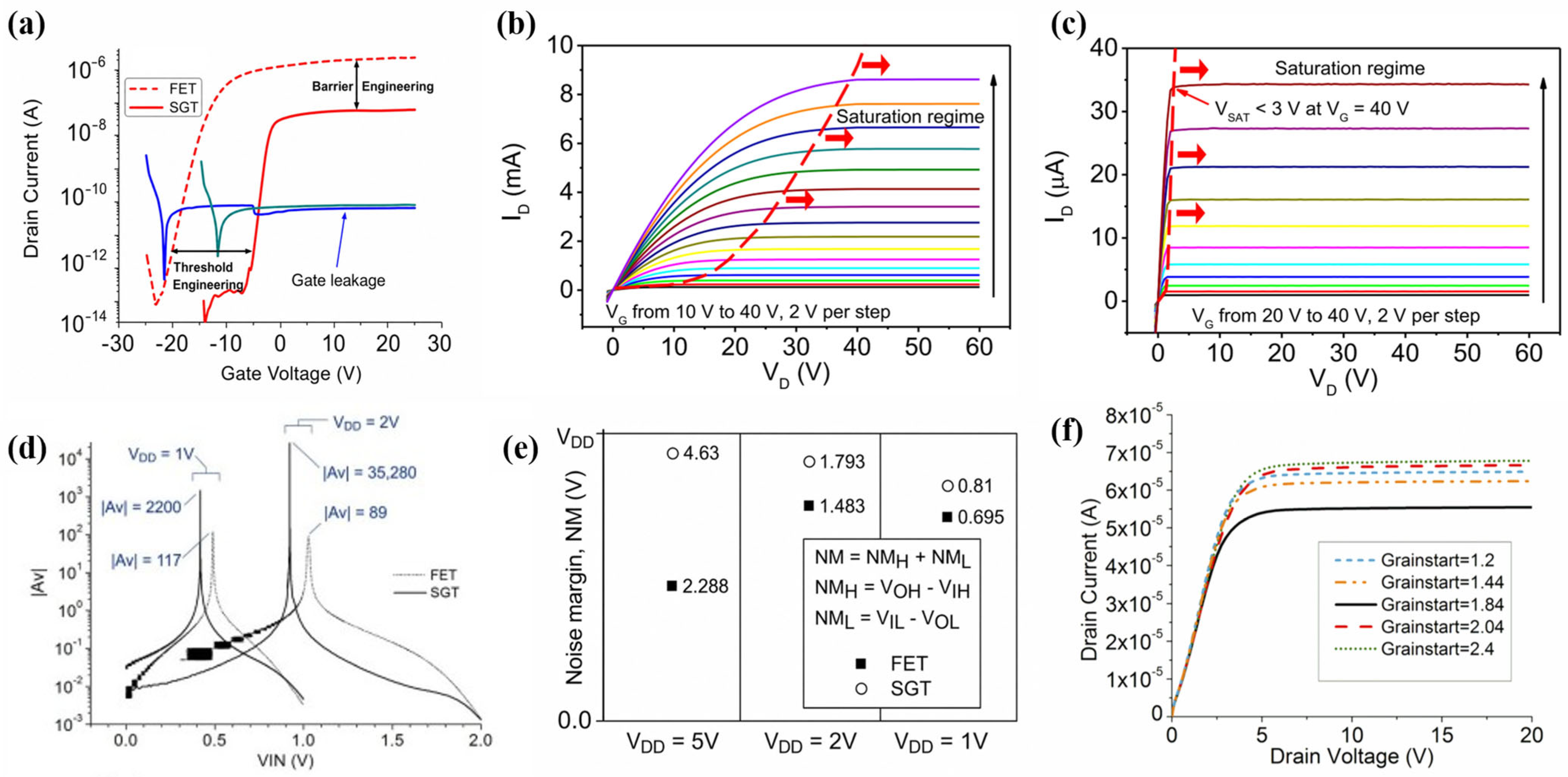
This section catalogs the electrical signatures that distinguish source-gated transistors from conventional thin-film transistors operating on the same channel material set: low drain saturation voltage, high output resistance and intrinsic voltage gain, and scaling behavior compatible with multi-tier yield budgets (Figure 1).

2.1. Strong Current Saturation and Low-Voltage Operation

The most distinctive signature of SGTs is exceptionally early drain-current saturation. SGTs reach saturation at drain voltages as low as under 2 V, whereas conventional FETs fabricated under comparable conditions require at least more than twice this voltage [36]. The gate-bias dependence of the saturation voltage is correspondingly weak, approximately 0.16 V per 1 V of gate-bias change, more than six times smaller than in the FET counterpart, confirming that saturation is set by the source contact rather than by drain-side channel pinch-off [36]. This early, source-controlled saturation persists across a remarkably wide range of source-drain spacings (2–60 μm) in polysilicon SGTs, demonstrating that low-voltage operation is achieved without aggressive lateral scaling and the associated fabrication-cost penalty [59].

2.2. High Output Impedance and Voltage Gain

In addition to low-voltage operation, SGTs exhibit extremely small output conductance ( g d ; i.e., large output impedance) and, consequently, a high intrinsic voltage gain. Maximum voltage gains ( A V ) of approximately 85 were reported in an early experimental work [36], which is about twice that of conventional FETs under similar conditions. Subsequent studies have revealed that increasing the drain voltage from 5 V to 10 V could further boost the voltage gain to values approaching 1000 [43]. Continued advances in device design and materials have led to even more dramatic improvements: self-aligned polysilicon SGTs demonstrated gains on the order of 5000 [60], while oxide-semiconductor SGTs based on Indium Gallium Zinc Oxide (IGZO) achieved experimentally measured intrinsic gains as high as 29,000 [40]. From a circuit-level perspective, this combination of high intrinsic gain and low-voltage operation enables SGTs to drive comparatively large loads while minimizing loading effects in analog amplifier stages [58].

2.3. Scaling, Reliability, and Process Compatibility

SGTs also exhibit favorable scaling behavior, retaining their key characteristics as device dimensions are reduced. Stable operation has been demonstrated and confirmed the scalability across a wide range of material systems, including polysilicon devices with channel length down to ~250 nm [61], IGZO down to ~360 nm [40], and 2D materials as short as 135 nm [62]. More recent studies have shifted the focus from the minimum achievable channel length to the stability of device performance after scaling. TCAD simulations of IGZO-based SGTs revealed that even with the channel length ≈500 nm, the increase in leakage current remains minimal compared to conventional TFTs [42]. Specifically, when sweeping the drain voltage at a fixed gate bias ( V G S = 5 V), the drain current increase ratio in SGTs was only 0.8%, whereas conventional TFTs exhibited a much larger increase of 23.7% under the same scaling conditions. This robustness is particularly significant for vertically stacked architectures, where per-tier yield enters multiplicatively into the overall stack yield; channel-length variation tolerance therefore becomes a system-level prerequisite for multi-tier integration rather than a per-device convenience.
From a manufacturing perspective, SGTs offer a further advantage in that they can be implemented using existing FET fabrication processes with only minor modifications, without the need for additional costly equipment. This high degree of process compatibility, as well as the relaxed dimension scaling, makes SGTs economically attractive [58]. Even in nanostructured implementations employing nanowires or nanosheets, where parasitic FET effects can degrade off-state performance, SGTs have been shown to maintain stable current flow, intrinsic gain, and effective mobility under gate-bias stress and stable current flow under temperature variation [63,64,65].

3. Operating Principles and Design Space of SGTs

This section develops the physical mechanism of source-gated operation, the architectural classes through which the source barrier is implemented, the channel-material platforms across which these architectures have been realized, and the spatial characterization techniques required to verify source-controlled operation experimentally.

3.1. Core Operating Principles

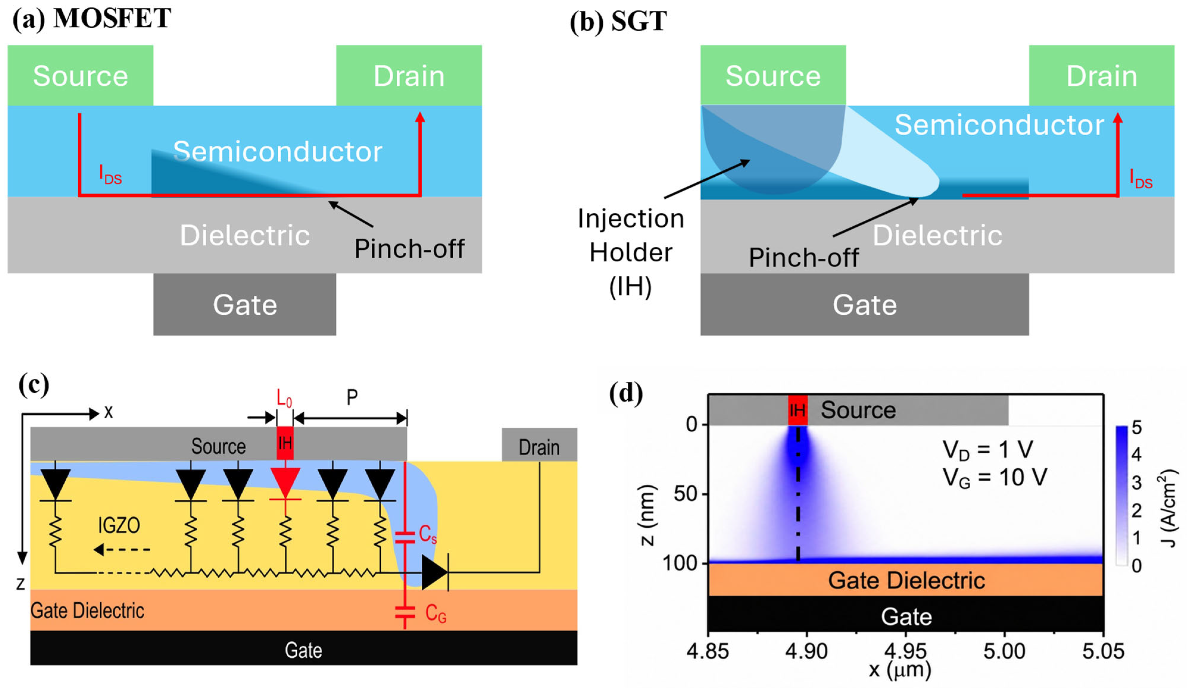
A source-gated transistor is a thin-film transistor architecture in which a carrier-injection barrier is intentionally introduced at the source–channel interface—typically a Schottky barrier formed by a high-work-function source metal or a metal–insulator–semiconductor (MIS) tunnel contact formed by inserting a thin insulating interlayer. Unlike conventional FETs, where the drain current is set primarily by gate-controlled channel conductance and saturation arises from drain-side pinch-off [32,33,34,35], in an SGT, the gate electrode overlaps both the source contact and the underlying reverse-biased Schottky junction, and current saturation is governed by gate-modulated injection across this source barrier rather than by electrostatic pinch-off near the drain (Figure 2a,b) [36,38,48].
During operation, at a given gate bias ( V G S ), the depletion region originating near the drain-side edge of the source expands toward the semiconductor/dielectric interface as the drain bias ( V D S ) increases. Once this depletion region reaches the interface, the channel near the source undergoes pinch-off, leading to current saturation ( I D S ) [38]. Thus, in SGTs, the current is primarily controlled by modulating the electric field across the source barrier using the gate voltage. This mechanism contrasts with that of conventional FETs, where current saturation occurs only when pinch-off develops near the drain end of the channel. In SGTs, however, pinch-off occurs near the source region first, enabling much earlier and stronger current saturation. By applying a gate voltage ( V G S ), electron or hole carriers are accumulated and confined in the semiconductor layer at the interface with the gate dielectric, leading to the formation of a conductive channel [58]. Upon applying a bias between the source and the drain ( V D S ), the accumulated carriers drift from source to drain electrodes, and generate the drain current ( I D ). I D increases with increasing V G S and V D S until reaching saturation when V D S is sufficiently large to pinch off the channel near the drain end [38].
Lee et al. employed Silvaco ATLAS 2D drift–diffusion Technology Computer-Aided Design (TCAD) simulations to reproduce the experimental characteristics of their oxide/organic SGTs, revealing the fundamental operation by visualizing carrier distribution and electrostatic depletion at the source junction. A key finding was the strong dependence of device performance on the source length ( L S ) , while the drain length ( L d ) had negligible impact, confirming the source-gating mechanism. The study further showed that in interdigitated electrodes, the effective contact length is reduced, which was captured by subdividing the geometry into Source-Drain and Drain-Source-Drain components for accurate current reproduction. Through parameter fitting, the authors extracted critical physical parameters governing the contact-limited operation, such as the injection barrier and carrier mobility. These results explained the fundamental origin of early saturation and the low saturation coefficient, highlighting how geometric factors like contact length determine the saturation behavior required for low-voltage operation. Overall, this work illustrates how TCAD can complement experiments by quantifying key contact-controlled parameters to elucidate the operational principles of SGTs and offering design guidelines for low-power, high-gain thin-film electronics [66].
SGT architectures can mitigate short channel effects and enhance current saturation, which is particularly beneficial for impedance matching in high-speed amplifiers and radio frequency (RF) circuits. This advantage is achieved through field-relief, where the source contact partially overlaps the channel region. In conventional FETs, the depletion region typically forms only near the drain contact. In contrast, in SGTs, a depletion region first emerges near the source contact under low drain bias ( V D ), while an additional depletion region appears near the drain contact at higher V D . As a result, SGTs exhibit ideal current saturation and significantly improved immunity to short-channel effects such as channel-length modulation [62].
Furthermore, simulation studies demonstrated that introducing a 1 µm-long field plate separated from the semiconductor by a 20 nm SiO2 dielectric realizable within standard lithographic design rules enhances the saturation characteristics of SGTs without adding fabrication complexity. SGT-based circuits at V D D = 5 V exhibit higher gain and improved noise margins compared to conventional FET circuits. The gain enhancement arises from the lower output conductance ( g d ) in the saturation region, directly attributed to the field relief structure [58]. Although the simulated SGT uses a relaxed dimension of 1 μm-long source field plate within a 4 μm source–drain gap, its extremely low output conductance leads to a much flatter saturation region than that of a conventional FET with the same geometry. This low-voltage saturation is not primarily determined by channel-length scaling, but by source-barrier control and source-side pinch-off. In this sense, the SGT can provide output characteristics and voltage gain that would otherwise require a substantially scaled TFT/FET channel, potentially in the order of tens of nanometers. In conventional TFTs, channel-length scaling is often required to achieve sufficient output saturation within a given operating-voltage window. However, excessive scaling eventually introduces short-channel effects, which increase the output conductance and reduce the output resistance and intrinsic voltage gain. In contrast, SGTs can achieve strong low-voltage saturation even at relatively long channel lengths through source-barrier control and field-plate-assisted drain-field screening. This demonstrates that high gain can be achieved through source-barrier control and field-plate-assisted drain-field screening, without significantly scaling device dimensions or fabrication complexity.
In source-gated transistors, current saturation is ultimately determined by the formation of source-side pinch-off, which arises from the interplay between the source barrier height, channel doping concentration, and channel thickness through their combined effect on the source-side depletion region length. The effective source barrier height ( Φ B ) and the channel doping concentration primarily set the extent of depletion beneath the source contact: a higher Φ B and lower doping concentration increase the depletion width by reducing the available mobile charge that can screen the source junction. As a result, the lateral depletion region extending from the source penetrates deeper into the channel under drain bias, lowering the drain voltage required to reach pinch-off.
Whether this depletion leads to effective current saturation further depends on its relationship with the channel thickness. When the depletion region extends across the full thickness of the channel, carriers are fully depleted beneath the source contact, establishing source-side pinch-off and stable current saturation. In thin-channel devices, this condition is readily satisfied even for moderate barrier heights, enabling early saturation and strong gate control. In contrast, in thicker channels, the depletion region may not fully span the channel thickness, allowing residual conduction paths to persist and weakening source-controlled operation. Consequently, the onset and robustness of pinch-off are governed not by any single parameter, but by the relative magnitude of the depletion region length compared to the channel thickness.
This coupling highlights that SGT operation is fundamentally an electrostatic problem in which barrier height and doping define the depletion length, while channel thickness determines whether that depletion can fully pinch off the channel. Optimal SGT design therefore requires co-optimization of these parameters to ensure that source-side depletion dominates transport, achieving early saturation and low-power operation without relying on aggressive lateral scaling.

3.2. Source Barrier Architectures

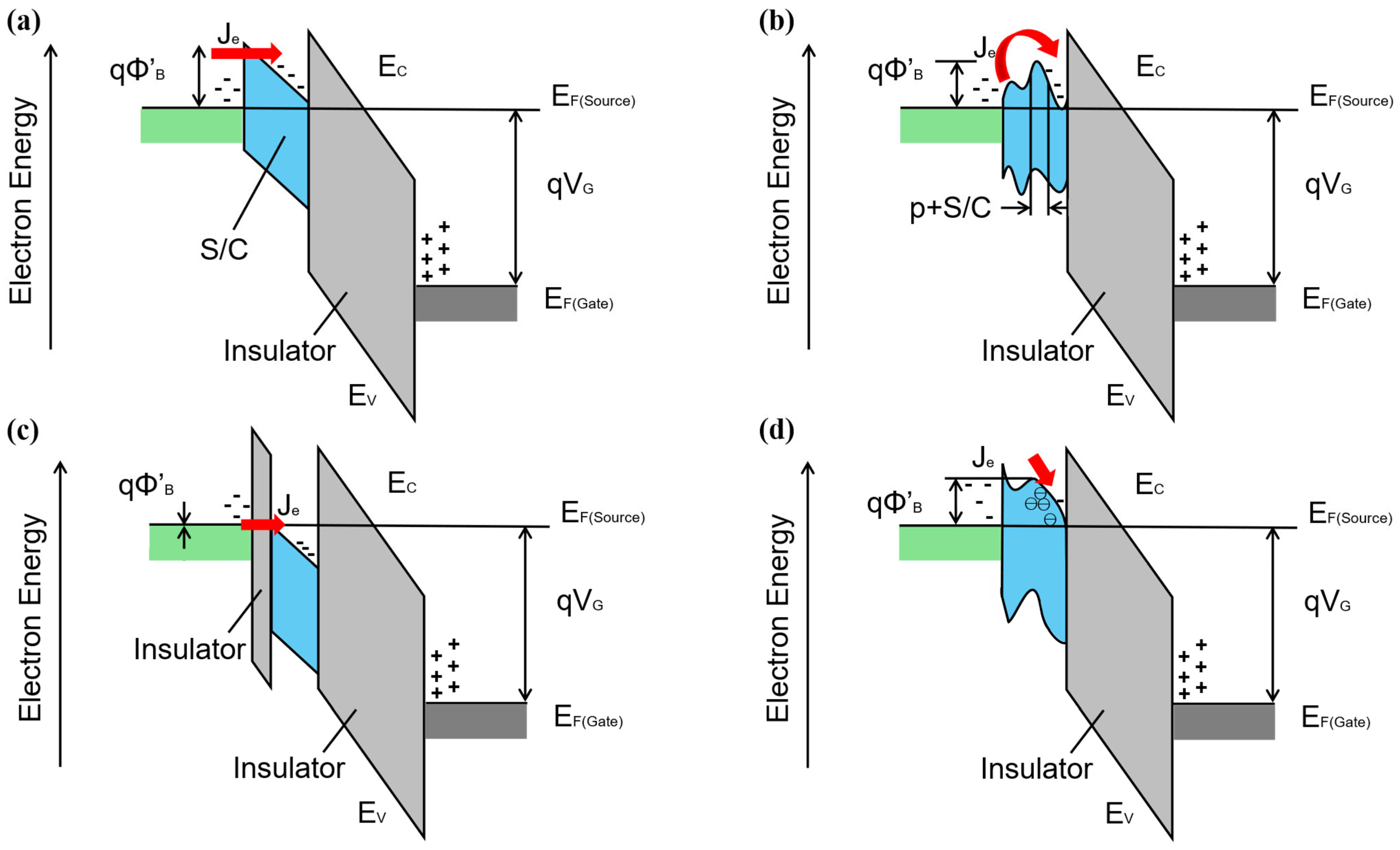
The defining feature of an SGT is the source barrier, which sets the height and extent of the depletion region responsible for source-side pinch-off and, consequently, the device transconductance (gm). As originally demonstrated by Shannon and co-workers, SGTs are controlled by modulating the depletion region beneath a reverse-biased Schottky barrier, which saturates the current injection [36]. Figure 3 illustrates four representative physical mechanisms for realizing source-controlled injection: (a) a Schottky barrier, (b) an intentionally engineered unipolar semiconductor barrier, (c) an MIS tunneling barrier, and (d) a space-charge-limited source relevant to semiconductors with a high density of trap states. The key distinction is that Figure 3b employs a pre-existing unipolar potential barrier within the semiconductor, whose height can be modulated by the gate field, whereas Figure 3d does not rely on such an engineered bulk barrier. Instead, it represents a space-charge-limited source relevant to high-trap-density semiconductors, where injected and trapped carriers establish the space charge that limits current, and the gate controls the associated electric field and space-charge magnitude. In the architecture-based classification adopted in subsequent SGT studies, the first three concepts are categorized as Schottky-barrier SGTs (SBSGTs), Bulk-barrier SGTs (BUSGTs), and Tunnel-contact SGTs (TSGTs), respectively, an additional physical realization of source-controlled injection that is not treated as a separate architecture class in the subsequent discussion [36,67] (Table 1).
Schottky-barrier SGTs. For conventional SBSGTs (Figure 3a), a metal–semiconductor Schottky barrier directly serves as the source injection barrier. The barrier height can be readily engineered through the source-metal work function and semiconductor properties, depending on the metal in contact with the source. Furthermore, the threshold voltage can be effectively tuned through bulk semiconductor doping and gate work function engineering [44,68]. Additionally, it has the advantage of low output conductance ( g d ), as mentioned in the characteristics of the previous SGT, thereby enabling high intrinsic voltage gain even at low operating voltages.
Tunnel-contact SGTs. TSGTs (Figure 3c) introduce a thin insulating layer at the source–semiconductor interface to form a metal–insulator–semiconductor (MIS) injection barrier [36]. Compared to conventional SBSGT, it employs an MIS barrier by inserting a thin insulating layer at the source contact region. Structurally, a nanometer-scale insulating layer, such as 3 nm Al2O3, is inserted directly between the source electrode and the semiconductor, thereby separating the injection barrier from the gate dielectric [45,46,47,67]. These devices have major features of fundamental SGTs, including low voltage saturation and tolerance of geometric structure. Despite utilizing a tunneling mechanism, this device exhibited a stronger-than-expected temperature dependence, indicating that the transport mechanism cannot be described by simple tunneling alone. Subsequently, by applying the same MIS tunnel contact concept to a 2D Transition Metal Dichalcogenide (TMD) channel, TCSGT achieved stronger contact controlled characteristics. This was realized by suppressing Fermi-level pinning (FLP) to enable effective Schottky barrier height (SBH) modulation via the source metal’s work function [48,49,50]. Furthermore, the optimization of the tunneling layer thickness played a crucial role in lowering the saturation voltage by enhancing the gate-field coupling at the source, significantly outperforming conventional SGTs [38,41]. Specifically, the metal and the WS2 channel were physically separated by a tunneling layer, thereby minimizing the penetration of the metal electron wavefunction and the induced gap state (DIGS). Due to these contact-controlled mechanism characteristics, an ultra-low saturation voltage of approximately 0.12 V and a low power operation of 1.2 nW were achieved. Based on this, the developed devices effectively utilize the ‘direct tunneling’ mechanism to maintain stable voltage saturation characteristics even under extreme conditions of 160 K.
Bulk-barrier SGTs. Lastly, BUSGTs (Figure 3b) realize the source injection barrier within the semiconductor rather than at the metal–semiconductor interface. Such barriers can be formed through controlled doping or semiconductor heterostructures [51]. In contrast to the traditional Schottky contact barriers, these barrier designs employ ohmic source contacts as a means of minimizing contact resistance [52,69]. While there may be some differences in the process steps for creating each bulk layer, the overall mechanism offers the advantage of an ‘ohmic contact’, which can effectively lower the interfacial contact resistance. This enables the material to exhibit higher on-current ( I o n ) and larger transconductance characteristics compared to conventional methods [70,71]. Furthermore, this enables an expanded, meaningful ‘dynamic range’ for drain current and low temperature dependence, potentially resulting in a lower temperature coefficient for drain current ( I D ). However, due to stability issues such as excessive positive threshold shift, which also causes reliability problems and a softer I D , s a t curve between output and transfer characteristics, this may somewhat reduce the utilization efficiency of low-power devices. Of course, it presents harder process challenges than existing SGTs, e.g., it requires intentionally creating a hump in the conduction band within the semiconductor layer to insert a bulk layer. Although various process challenges exist, the greatest advantage of this device is that its design parameters are more diverse than other types of SGT. This diversity enhances the potential for versatile applications and performance optimization in actual device fabrications and utilization. Although experimental heterostructure BUSGTs have been demonstrated, the architecture remains considerably less explored than conventional Schottky-barrier SGTs, and further work is required to establish robust material systems, reproducible barrier formation, and scalable fabrication.

3.3. Channel Material Platforms

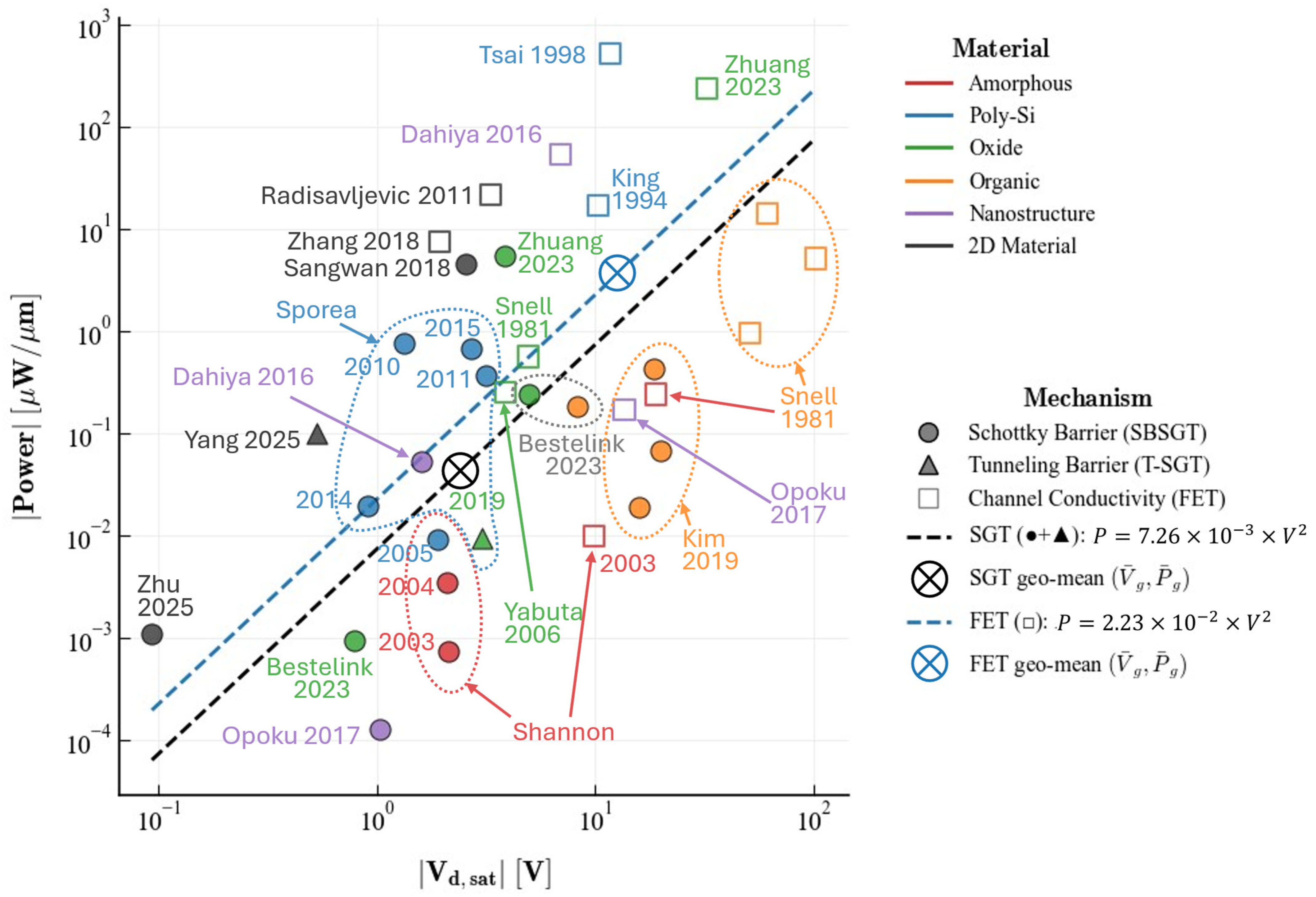
The comparative dataset in Figure 4 was compiled from reported SGT, FET, TFT, and MOSFET characteristics in the literature. Most data points were obtained from references discussed in the main text, while additional sources were included to supplement device categories with insufficient comparison data [72,73,74,75,76]. Values were extracted from the transfer and output characteristics of fabricated devices; when numerical values were not explicitly reported, they were estimated from published curves. Because material properties, device geometries, and operating mechanisms vary widely across the selected devices, some outliers are present in the plot. Nanowire- and nanosheet-based devices were classified separately, as their electrical characteristics can be strongly affected by structural effects rather than by material properties alone. MOSFET reference data were also included for comparison based on reported device characteristics.
SGT operation is not intrinsically restricted to a specific semiconductor material. In principle, source-controlled transport can be realized in any material platform in which the key parameters governing source depletion and carrier injection—such as source-barrier characteristics, depletion width, semiconductor thickness, source geometry, and gate-field coupling—can be appropriately engineered. The material choice therefore determines the accessible design window rather than the fundamental applicability of the SGT concept. SGT naturally differentiates its application spectrum based on channel material selection due to its structural characteristics of source barrier control. The a-Si:H-based approach has primarily been discussed for large area, low cost backplanes based on its low temperature process and TFT line compatibility [82,86], while the poly Si base demonstrates advantages in driving high resolution displays and relatively high speed circuits due to its high mobility, though process temperature constraints are noted [43]. Poly Si requires high process temperatures for crystallization and annealing, limiting their application in flexible and low-cost substrates. In poly Si SGTs, source length selection creates a trade-off between speed and process sensitivity [38,59,78,79,87]. Oxide based materials like IGZO achieve uniformity, transparency, and medium to high mobility, emphasizing their suitability for next generation displays, transparent electronics, and low power circuits. Advantages in stability and leakage suppression during miniaturization have also been reported [40,42]. Beyond IGZO, source-controlled operation has also been demonstrated in other oxide semiconductors such as In2O3, indicating that the SGT concept is applicable across chemically and electronically distinct metal-oxide channels. Organic semiconductor based materials, leveraging solution/low temperature processes and mechanical flexibility, are actively utilized in flexible, wearable, and printable electronics [81,88,89,90,91]. Organic SGTs likewise encompass chemically distinct semiconductor classes, including small-molecule systems such as Ph-BTBT-C10 and Ph-BTNT-C10 and conjugated-polymer channels, demonstrating that source-controlled transport is not restricted to a particular molecular structure or transport framework.
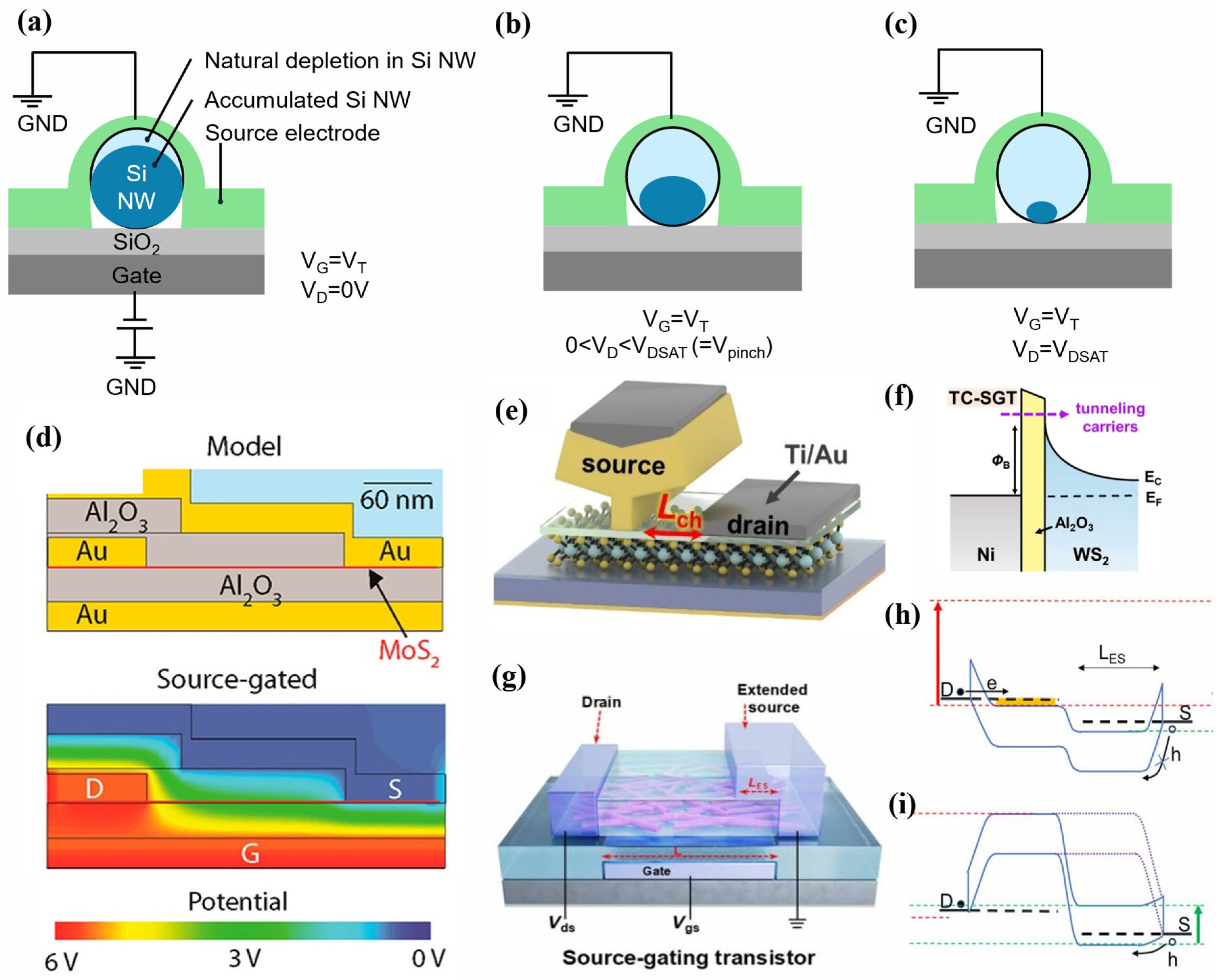
Representative SGT implementations using low-dimensional channel materials are shown in Figure 5. Panels (a–c) illustrate source-controlled depletion and pinch-off in a Si nanowire SGT, panel (d) shows a self-aligned short-channel (SASC) MoS2 transistor, panels (e,f) present a WS2 tunnel-contact SGT, and panels (g–i) illustrate a CNT-SGT and its source-controlled band modulation. While nanostructure e.g., nanowire and nanosheets based (Si, ZnO, etc.) approach, combined with solution/low temperature processes, are steadily being reported for expansion into printable, low power devices, sensors/photodetectors, and flexible electronics [56,84,92]. A separate consideration arises specifically for low-dimensional channels (e.g., TMDs, Carbon Nanotube; CNT). Conventional 2D FETs typically exhibit weak current saturation under standard biasing. Low charge density and contact-dominated transport in low-dimensional channels can complicate the formation of robust conventional drain-side pinch-off [41,62,83,93]. When incorporated into SGT architectures, however, these materials can recover strong current saturation because the saturation onset is governed by the source barrier rather than by drain-side processes [41]. In atomically thin channels, the key challenge is therefore to maintain sufficient electrostatic control over the source barrier despite metal-contact screening and Fermi-level pinning; source-extended gate geometries and self-aligned tunnel contacts have been employed to enhance barrier width and gate tunability, enabling robust saturation in 2D SGTs.
Beyond the thin-film and low-dimensional material platforms discussed above, related source-depletion concepts have also been demonstrated in wide-bandgap III–V devices. For example, a Schottky source extension incorporated into a p-GaN HEMT was shown to induce source-edge pinch-off and limit the saturation current at high drain bias [94]. Although developed primarily for short-circuit protection rather than low-voltage operation, this result illustrates that source-side depletion control can be extended beyond conventional TFT-based SGT material systems.

3.4. Spatial Characterization of SGT Operation

Experimental identification of SGT operation requires explicit separation of source and drain side transport mechanisms, which cannot be fully captured by conventional FET current voltage (I–V) characteristics alone. While standard output and transfer measurements provide initial indications of early current saturation, they offer limited insight into whether saturation originates from source barrier modulation or from drain side channel pinch off. Likewise, commonly used contact analysis techniques, such as transmission line measurements (TLM) for contact resistance extraction or temperature-dependent Schottky barrier height analysis, are primarily designed to quantify static contact properties and are insufficient to accurately identify the bias conditions under which source-side pinch-off occurs in SGTs. These methods generally lack spatial resolution and do not directly probe the gate-controlled evolution of the depletion region at the source, making it difficult to unambiguously distinguish contact-limited operation from conventional channel-limited behavior.
Beyond conventional electrical characterization, spatially resolved measurement techniques provide direct and unambiguous experimental evidence of SGT operation by visualizing source-controlled injection mechanisms. Techniques such as (Operando-) Kelvin probe force microscopy (KPFM), scanning photocurrent microscopy (SPCM), and electron-beam-induced current (EBIC) mapping have been employed to probe the electrostatic potential and carrier collection near the source contact with nanoscale resolution [77,95,96].
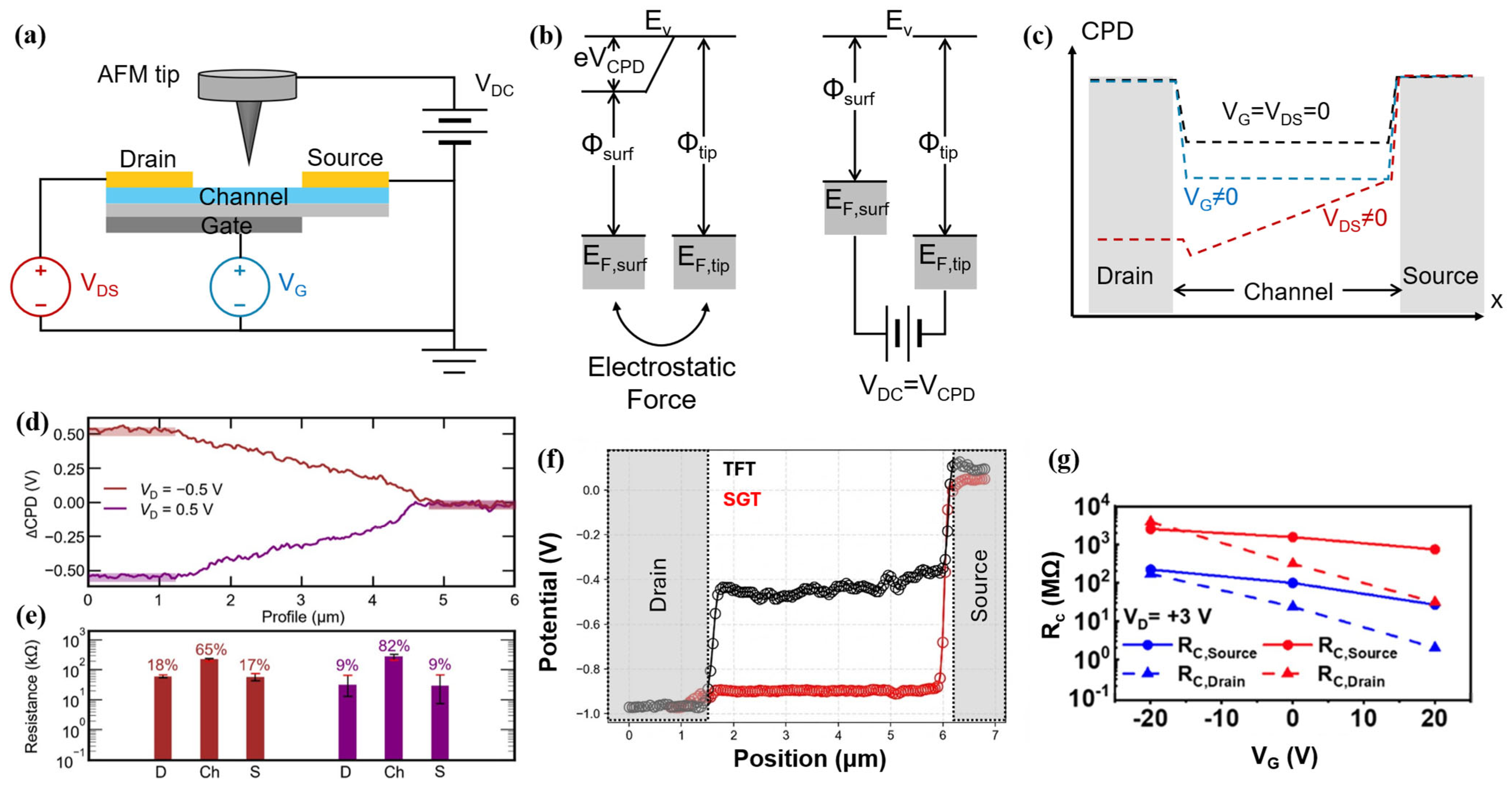
Operando Kelvin Probe Force Microscopy. Operando KPFM measures the local contact potential difference (CPD) between a conductive Atomic Force Microscope (AFM) tip and the device surface while the transistor is biased, thereby mapping the quasi-Fermi level distribution and surface potential under actual operating conditions. By applying a voltage to nullify the electrostatic force between the tip and sample, KPFM directly extracts the spatial variation of surface potential with sub-100 nm resolution. When performed under simultaneous gate and drain bias (“operando” condition), this technique enables direct visualization of the bias-dependent potential drop and depletion evolution near the source junction [97]. Figure 6 summarizes the operando KPFM measurement principle and representative spatial analyses for identifying source-controlled transport. Panels (a–c) illustrate the measurement configuration and CPD-based potential analysis, while panels (d–g) present representative potential-profile and resistance analyses showing source-side voltage localization and source-dominated current control.
These measurements directly reveal the formation of a lateral depletion region extending from the source electrode, whose spatial extent and potential profile are strongly modulated by the gate bias. Representative Operando KPFM studies on solution-processed metal oxide SGTs demonstrate that the dominant potential drop is localized at the source contact rather than near the drain, in clear contrast to conventional thin-film transistors [77]. KPFM potential maps showed that polymer doping of In2O3 channels enhances the source-side potential drop, indicating strengthened gate-controlled modulation of charge injection at the source. Despite a geometrically symmetric device structure, the observed asymmetric potential distribution confirms that current saturation originates from source-side pinch-off governed by the Schottky contact.
In practice, source-controlled operation can therefore be evaluated by comparing KPFM potential profiles across drain biases below and above the apparent saturation voltage. Since reliable interpretation requires an exposed electrode–channel geometry, the work-function difference between the probe and the exposed electrode/channel surface under each gate bias is first measured and used as a baseline reference. The measured CPD is then referenced to this baseline to isolate only the bias-induced voltage drop across the device. Persistent localization of a substantial fraction of the extracted potential drop near the source, together with only limited redistribution across the remaining channel after saturation, supports source-controlled transport, whereas an increasing drain-side potential drop is more consistent with conventional channel pinch-off.
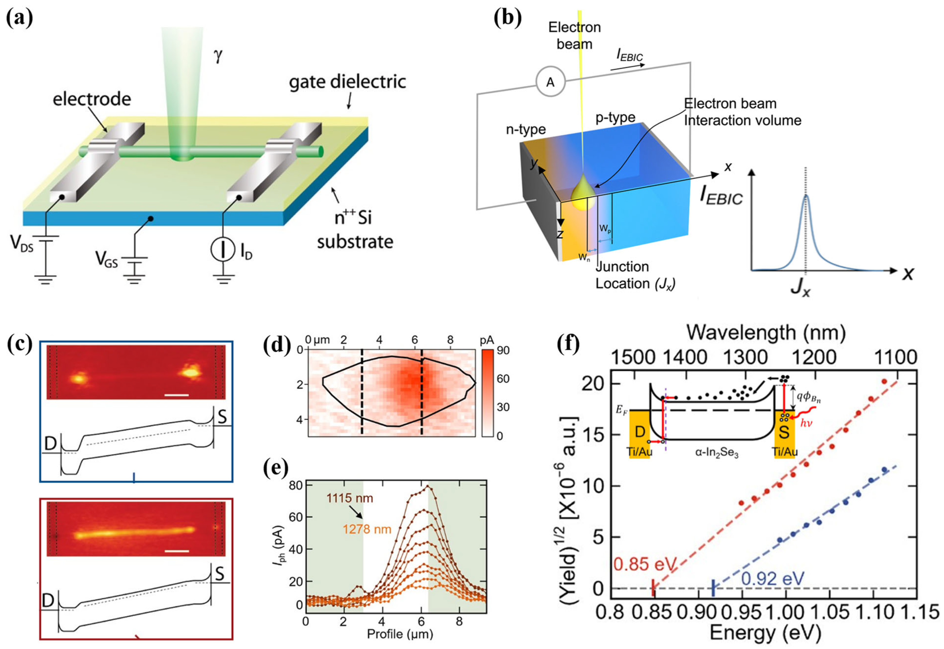
Scanning Photo Current Microscopy. SPCM, in contrast, relies on localized optical excitation to generate electron-hole pairs, whose separation by built-in or bias-induced electric fields produces a measurable photocurrent [95,99]. Because the photocurrent magnitude is proportional to the local electric field and carrier collection efficiency, SPCM provides a direct map of internal electric field distribution. The SPCM measurement principle and representative spatial photocurrent analyses are illustrated in Figure 7a,c–f. In SGTs, a pronounced photocurrent peak is expected at the source-edge region where the reverse-biased Schottky barrier creates a strong depletion field, whereas the drain side—often designed to be quasi-ohmic—should exhibit comparatively weak signals. For practical validation, SPCM maps should be compared as the drain bias is increased through the onset of current saturation. Persistent localization of the dominant photocurrent response near the source edge supports source-barrier-controlled operation, whereas the emergence or migration of a strong response toward the drain side would be more consistent with drain-side channel pinch-off.
Similarly, EBIC employs a focused electron beam within a scanning electron microscope to generate carriers inside the semiconductor, enabling subsurface mapping of electrically active junctions [100,101]. A representative EBIC measurement scheme for spatially identifying electrically active junctions is shown in Figure 7b. The resulting EBIC signal highlights regions with strong space-charge fields, making it particularly suitable for identifying buried source junctions and quantifying depletion width. Although comprehensive EBIC studies on SGTs remain limited, one can reasonably anticipate that EBIC mapping would reveal a pronounced and spatially extended signal at the source junction, directly correlating with the depletion-controlled injection mechanism, while the drain contact would display minimal contrast.
Figure 7. SPCM and EBIC analyses for spatially resolved carrier-transport characterization. (a) SPCM measurement configuration for a nanowire transistor using localized optical excitation. (b) EBIC measurement principle, where electron-beam-induced carrier generation produces a spatially resolved current peak that identifies the electrically active junction. (c) Representative photocurrent maps and corresponding band profiles showing contact-localized photoresponse. (d) Two-dimensional photocurrent map resolving the spatial distribution of carrier separation along the device. (e) Wavelength-dependent photocurrent line profiles illustrating the evolution of the local photoresponse with excitation wavelength. (f) Photoresponse-yield analysis as a function of photon energy, used to extract the effective Schottky-barrier energies from the spectral threshold. Adapted/reproduced with permission from Allen et al. [99], Chu et al. [95], and Zhou et al. [102].
Electronics 15 03824 g007
Overall, spatially resolved measurements provide real-space verification that current saturation in SGTs arises from gate-controlled source barrier modulation rather than drain-side channel pinch-off, thereby complementing electrical transport data and establishing the physical basis of contact-limited operation across diverse material systems. In practice, the spatial validation framework should be applied by correlating the electrical onset of saturation with the bias-dependent location of the dominant potential drop or high-field region. Together, Operando KPFM, SPCM, and EBIC offer complementary insight, where KPFM resolves the electrostatic potential landscape, and SPCM and EBIC visualize electric-field-driven carrier separation at the buried junction, forming a comprehensive framework for experimentally validating source-controlled transport in SGT architectures.

4. Applications

The four observations laid out in the introduction, i.e., material accommodation, low VD,sat, channel-length variation tolerance, and architectural diversity, translate into two distinct application directions: (i) standalone edge electronic devices that exploit SGTs’2 intrinsic low-power and high-gain operation, and (ii) upper-tier devices in monolithic 3D integrated systems that exploit SGTs’ BEOL compatibility and multi-class architectural realizations. The former has been comprehensively reviewed elsewhere [38,58] and is summarized here only briefly; the latter is developed below as the central application thesis of this review.
It is notable that the technological maturity of these application directions differs substantially. Edge-electronic applications represent the most experimentally established use of SGTs, with demonstrations at the device and small-circuit levels. However, these implementations remain predominantly laboratory-scale rather than commercially deployed technologies. In contrast, SGT-based M3D upper tiers remain at a pre-integration stage. BEOL-compatible SGTs and relevant M3D material/process platforms have been demonstrated separately, but their integration into a functional multi-tier system has not yet been demonstrated. Memory-integrated SGTs for CIM and neuromorphic functions are currently at an early device-level proof-of-concept stage. The principal remaining barriers include large-area source-barrier uniformity and long-term reliability for edge devices; compact-model and design-infrastructure maturity, thermal management, and multi-tier process integration for M3D applications; and retention, endurance, multilevel-state uniformity, and array-level validation for memory-integrated SGTs, as discussed further in Section 5.

4.1. Edge Electronics

The electrical signatures of SGTs, namely low VD,sat, high output resistance and intrinsic voltage gain, and channel-length-variation tolerance, translate directly into a set of advantages at the edge of distributed electronic systems: low supply voltage, low static power, robust noise margins under fan-out, mechanical robustness on flexible substrates, and dark-current suppression in optical applications.
Heterogeneous-channel complementary logic. The first complementary SGT inverter built from heterogeneous channel materials—IGZO for the n-channel and the organic semiconductor for the p-channel—achieved a noise margin reaching 94% of the theoretical maximum [80], demonstrating that SGT logic maintains clearly discernible output levels under large fan-out even when the n- and p-channel materials are mismatched. The same principle of co-integrating mismatched channel materials within a single SGT framework generalizes directly to the heterogeneous-tier M3D vision in the following sections. The reliability and uniformity advantages previously noted additionally support SGTs in display driver circuits including Active-Matrix Organic Light-Emitting Diode (AMOLED) backplanes, where high output impedance and device-to-device uniformity are critical.
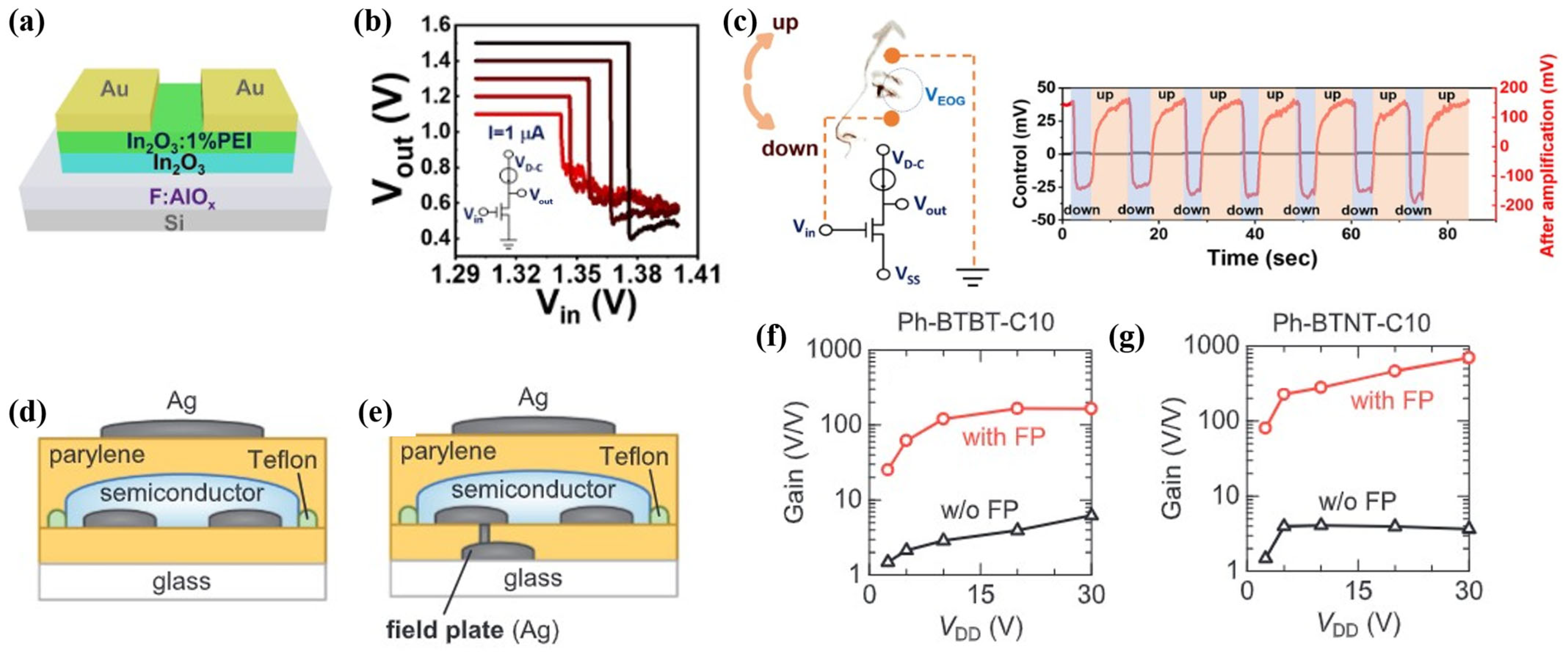
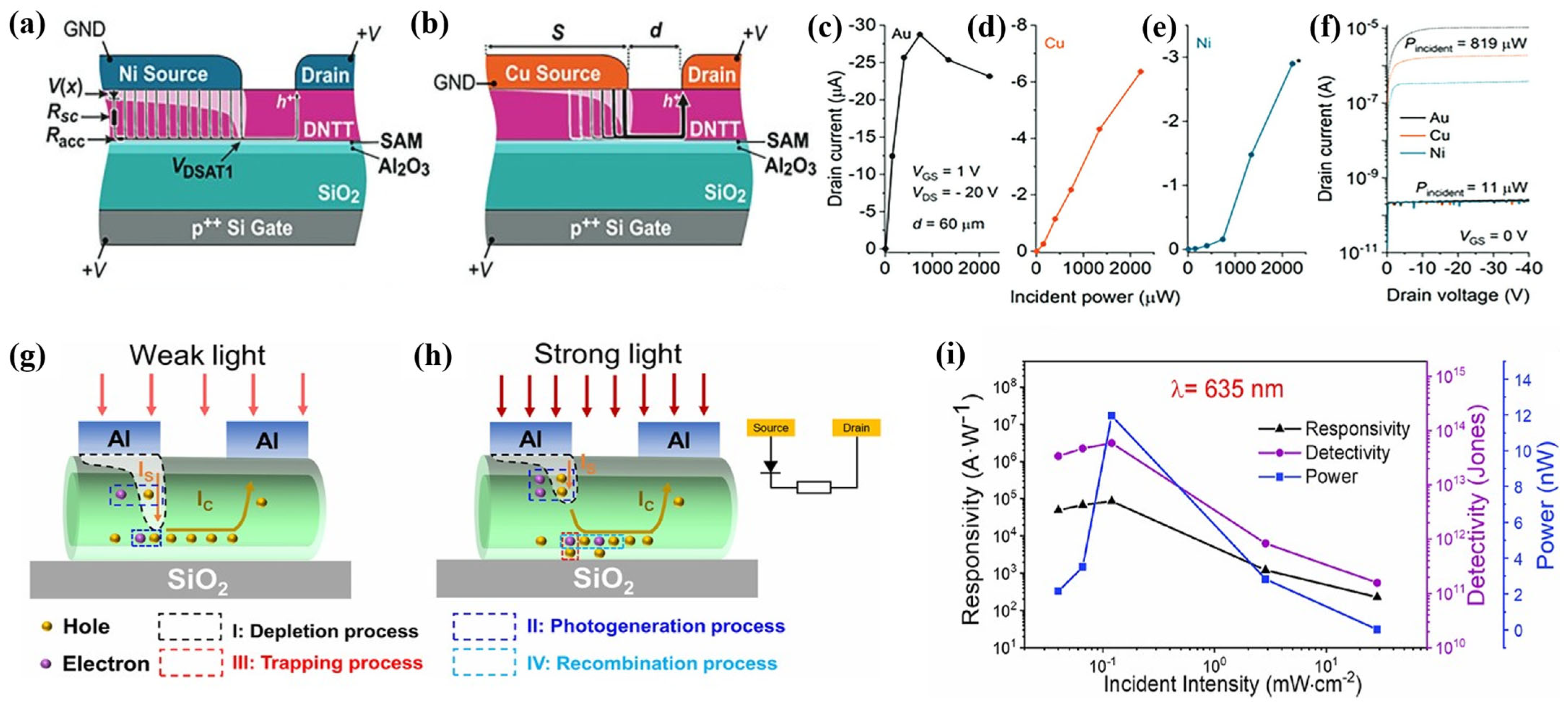
Ultralow-power amplifiers and analog front-ends. Across polysilicon and organic-semiconductor platforms, SGTs have been shown to deliver substantial improvements in gain, noise margin, power-delay product, and circuit robustness over conventional TFT-based circuits, motivating their use in biomedical sensors, civil-infrastructure monitoring, remote sensing, artificial skin, wearable computing, and lightweight space electronics [58,103]. Three demonstrations span the relevant power range. Schottky-barrier organic SGTs operated in source-gated mode have reached fully inkjet-printed amplifiers with voltage gain of 260 v/v at sub-1 nW power consumption, with signal-to-noise ratio (SNR) > 60 dB sufficient for human electrooculogram (EOG) acquisition and virtual/augmented reality human–machine interfacing [104]. Field-plate organic SGTs subsequently extended single-stage gain beyond 700 v/v on printed substrates, indicating that structural optimization alone can lift organic-semiconductor amplifiers to the precision-medical signal-processing range [105]. At still lower power, a two-transistor common-source amplifier based on Schottky-barrier SGTs delivered voltage gain exceeding 220 with output power below 150 pW, suitable for ultralow-power analog front-ends in implantable sensor interfaces [106]. Representative field-plate-assisted SGT amplifier architectures and their voltage-gain characteristics are shown in Figure 8d–g.
Flexible substrates and bio-signal monitoring. The signatures of SGT operation persist on flexible substrates. F:AlOX-gated solution-processed metal-oxide SGTs fabricated on polyimide retained 76.3% of initial ID,SAT and 94.5% of VD,SAT after ten bending cycles, supporting wearable and flexible electronics where mechanical durability is essential [77]. The same platform was used to amplify ~1.0 mV electrooculogram signals to over 300 mV using inverters with intrinsic gain exceeding 5000 [77], providing a direct path from device-level signatures to wearable medical sensing and human–computer interfacing. Figure 8a–c further illustrates a low-voltage F:AlOX SGT and its application to electrooculogram (EOG) signal amplification, demonstrating the potential of SGTs for low-power bio-signal monitoring.
Photodetectors and optoelectronic readout. The reverse-biased Schottky barrier in SGT architectures depletes the channel of carriers and suppresses dark current, a property essential for photodetectors operating at low drive voltages [107]. A representative GeS-nanowire SGT photodetector saturates at VD,sat = 0.61 V, consumes only 7.06 pW, and achieves detectivity of 5.87 × 10¹³ Jones together with a bidirectional photoresponse—positive photoconductivity switching to negative photoconductivity depending on incident-light intensity [108]. The device structure, low-voltage output characteristics, and light-intensity-dependent bidirectional photoresponse of this GeS-nanowire SGT photodetector are summarized in Figure 9. The combination of low drive voltage and high optical performance in a single device encapsulates the optoelectronic case for SGTs.

4.2. Monolithic 3D Integration

Motivation and constraints of M3D integration. Another promising application for SGTs is for upper tiers in M3D integrated circuits [14]. M3D integration is an emerging device concept where multiple layers of active devices are sequentially fabricated and vertically stacked on a single wafer, enabling three-dimensional system integration without relying on wafer bonding [17,109]. As transistor scaling and planar integration approach their physical limits, 3D integration has emerged as a promising strategy to extend system-level performance and functionality. Beyond simply multiplying areal transistor density, 3D integration offers greater freedom in transistor placement, enabling system-level optimization by vertically co-locating functionally-related devices and therefore reducing interconnect length, parasitic capacitance, and energy consumption [14,15,18,19,20,21]. Moreover, different tiers can be implemented using device materials tailored to specific functions, such as single-crystal silicon for high-performance logic and alternative semiconductors for memory, sensing, or control, allowing efficient partitioning of system functionality along the vertical dimension [6]. Most practical integration to date relies on chiplet-level stacking, in which dies fabricated on separate single-crystal silicon substrates are vertically interconnected using solder balls, micro-bumps, or hybrid copper bonds. While effective for heterogeneous integration, this packaging-based approach is fundamentally limited by relatively large vertical interconnect pitches (~μm) and alignment errors inherent to packaging processes. Simulation studies suggest that vertical via pitches on the order of ~10 nms are required to fully exploit the potential of 3D integration in terms of interconnect scaling and energy efficiency. Consequently, lithography-defined approaches that enable nanometer-scale vertical interconnects with precise alignment are gaining increasing attention as a pathway toward highly optimized three-dimensional integrated systems.
A key requirement for realizing M3D integration is the formation of active device layers above the BEOL interconnects of a fully fabricated lower-tier circuit. Because the thermal budget of commercial CMOS BEOL processing is typically limited to approximately 400 °C, the choice of channel materials and fabrication processes for upper device tiers is severely constrained. Consequently, M3D implementations predominantly rely on semiconductor materials that can be deposited or processed at low temperatures, such as amorphous silicon, oxide semiconductors, and 2D materials. While alternative schemes based on transferring single-crystal silicon layers have been explored, BEOL-compatible device layers generally exhibit lower carrier mobility and reduced charge density compared to bulk silicon.
SGTs as a complementary upper-tier device strategy. Rather than treating these material limitations as drawbacks, the aforementioned four signatures of source-gated operation address them directly: source-barrier electrostatics absorb the moderate mobility and nonideal contacts of low-temperature deposited channels; the low VD,sat provides the per-tier power headroom that vertical stacking demands; channel-length-variation tolerance addresses the multi-tier yield problem in which per-tier yield enters multiplicatively into overall stack yield; and the architectural diversity of source-barrier classes allows the upper-tier device family to be matched to distinct functional demands within a single fabrication framework. SGTs therefore convert M3D material constraint into a complementary device strategy in which high-performance single-crystal silicon transistors in the first tier are paired with low-power SGTs in the upper tiers, each optimized for its role. The heterogeneous M3D vision developed throughout this review (Figure 1) deploys this complementary strategy at the tier level. The first (front-end-of-line) tier hosts high-performance silicon CMOS for logic, cache, and high-frequency I/O. Upper tiers host two distinct SGT-based roles within the sub-400 °C thermal budget. A low-power upper tier built from oxide- or 2D-channel SGTs supports local logic, sensor read-out, analog front-ends, and always-on control—illustrated by sub-2 V solution-processed In2O3 SGTs with intrinsic gain > 5000 [77], 0.12 V TC-SGTs on WS2 channels at 0.12 nW power [41], and recent flexible monolithic 3D complementary circuits printed from 2D-semiconductor inks [22], all of which sit within the BEOL constraint set.
Power delivery and regulation. The same saturation physics that defines SGT operation also addresses a system-level power delivery constraint that vertical stacking amplifies. As tiers multiply, supply current must traverse increasingly resistive vertical interconnect networks, so that IR drop, supply noise, and tier-to-tier voltage non-uniformity become first-order design limits rather than secondary parasitics [14,18]. Conventional FET-based upper-tier circuits, whose drain currents retain appreciable VDS sensitivity even in nominal saturation, translate these supply fluctuations directly into logic-level and bias-point errors. An SGT, by contrast, behaves as a gate-programmed current source whose output is nearly invariant to drain bias above VD,sat; circuits built from such elements inherently reject supply ripple, relaxing the decoupling-capacitance and power-grid overhead that each additional tier would otherwise demand. The low absolute value of VD,sat compounds this advantage by lowering the per-tier supply rail itself, reducing both the conversion ratio required of on-chip voltage regulators and the resistive losses in the delivery network. The same property extends to the opposite end of the power spectrum: energy-harvesting-powered edge nodes operate from intrinsically unregulated and fluctuating supplies [5], and SGT-based front-ends and current references [58,103] retain calibrated operating points under such conditions without dedicated regulation stages. SGTs are therefore relevant to the power system at two levels simultaneously—as loads that tolerate imperfect power delivery within an M3D stack, and as circuit elements that simplify power management in energy-constrained edge systems.
Memory-integrated tiers for compute-in-memory and neuromorphic acceleration. Beyond logic and sensor read-out, the same heterogeneous-tier strategy extends to a third upper-tier role dedicated to compute-in-memory (CIM) and neuromorphic acceleration. Integrating a non-volatile memory mechanism into the source-injection barrier of an SGT converts its already voltage-invariant saturation current into a directly programmable state variable. Conventional memristors and memtransistors encode their state in linear-regime resistance or channel conductance, rendering their effective weights sensitive to read-bias variation, channel nonlinearity, and IR drops along the dense vertical interconnects of stacked architectures. A memory-integrated SGT instead defines an upper bound on the output current that, once saturation is reached, depends only weakly on drain bias, so the encoded state remains robust against read-bias and supply-voltage fluctuations within the stack. The source-barrier modulation is itself agnostic to the underlying memory physics: ferroelectric polarization in van der Waals or HfO2-based ferroelectric layers [53,54], charge trapping at engineered interfaces, and vacancy migration in resistive-switching oxides each provide distinct routes to non-volatilely tune source-side injection. The most concrete realization to date couples α-In2Se3 ferroelectric contacts with a monolayer MoS2 channel and achieves multi-level saturation-current programming with output impedance of approximately 8 GΩ at sub-1 V drain bias [55], and the spatial validation framework of Section 3.4 is well suited to verify that analogous mechanisms in alternative memory chemistries operate through source-barrier modulation rather than channel-side effects. Together with the FEOL silicon CMOS tier and the low-power oxide and 2D SGT tier, this memory-integrated SGT tier completes a three-tier heterogeneous M3D vision in which each tier is matched to a distinct functional role within a single BEOL-compatible fabrication framework.
On-device learning and the communication-energy budget. The system-level case for this three-tier vision is sharpened by the energy structure of edge intelligence itself. For distributed edge-AI nodes, wireless data transmission—not computation—frequently dominates the energy budget, which motivates processing raw sensor data locally and communicating only compact inference results or model updates [2]. Emerging training paradigms such as federated learning institutionalize this trade-off: model parameters are updated on-device and only weight increments are exchanged, shifting the workload decisively toward local, energy-constrained computation. The memory-integrated SGT tier described above is matched to precisely this workload. Non-volatile, multi-level programming of the saturation current provides analog weight storage and update capability within the BEOL stack [55], while the read-bias robustness of a saturated output current protects stored weights against the supply fluctuations inherent to battery- or harvester-powered operation—a failure mode that linear-regime resistive weights cannot avoid [110]. At the same time, the low-power SGT tier supplies the always-on analog front-ends that gate the communication radio itself: sub-nW SGT amplifiers [104,106] can continuously monitor sensor channels and wake the power-hungry transceiver only on relevant events, compressing the duty cycle of the dominant energy consumer. Within a single BEOL-compatible stack, SGT tiers thus support the full edge-intelligence loop—sensing, local learning, and communication gating—under the energy constraints identified at the outset of this review.

5. Challenges and Outlook

The preceding sections have argued that source-gated operation converts the material constraints of BEOL-compatible upper tiers into a coherent device strategy. A balanced assessment, however, requires confronting the limitations that currently separate SGTs from deployment in manufacturable M3D platforms. This section identifies four such challenges, namely drive current and dynamic performance, statistical uniformity of the source barrier, the absence of compact-model and design-automation infrastructure, and thermal management in vertically stacked tiers, and outlines the research directions through which each may be resolved.
Drive current and dynamic performance. The defining trade-off of the SGT is that early, source-controlled saturation is purchased with reduced on-current and transconductance relative to a conventional TFT on the same channel [38,58]. The dynamic consequences are twofold. First, the saturation current itself is barrier-limited, so large-signal slew rates and fan-out drive strength are lower than channel-conductance-limited devices can provide. Second, functional source-gating requires the source contact to overlap the gate, and this overlap contributes a parasitic capacitance that, together with the reduced transconductance, lowers the cutoff frequency [111]. Early analyses of a-Si:H SGTs placed the barrier-limited cutoff frequency ( f T ) in the low-megahertz range, becoming transit-time-limited near 20 MHz as the barrier is lowered or the gate field increased—adequate margin over the equivalent TFT for large-area analog tasks, but far from the gigahertz regime of the silicon tier below [38,58]. These bounds are not immutable: self-aligned geometries minimize the overlap beyond the depletion-defining region [60], tunnel-contact engineering raises injection efficiency while preserving saturation quality [41,67], and bulk-barrier architectures recover ohmic-level on-currents at the cost of process complexity [52]. The appropriate design target, however, is honesty about the role: in the heterogeneous M3D vision of this review, SGT tiers are not intended to compete with the FEOL silicon tier on speed, but to occupy the always-on, analog, and memory functions in which their low V D , s a t and high output impedance dominate the figure of merit. Quantitative f T and power-delay benchmarking of SGTs against conventional BEOL TFTs under identical thermal-budget constraints remains an open and important task.
Statistical uniformity of the source barrier. SGT operation concentrates device behavior into a single interface, and thermionic injection depends exponentially on the effective barrier height; barrier non-uniformities of only tens of meV therefore translate into substantial spreads in saturation current. The available evidence is encouraging but limited in scale. Contact-barrier engineering has been shown to improve current uniformity across polysilicon device populations precisely because barrier-limited injection masks the grain-boundary variability that dominates channel-limited devices [59], statistical studies of tunneling contacts on CVD MoS2 quantify the achievable barrier-height dispersion [44], and nanoscale contact engineering has improved thermal and bias-stress stability in IGZO SGTs [61]. Yet these data sets comprise tens of devices; the multiplicative yield arithmetic of multi-tier stacks demands barrier-height distributions characterized at wafer scale, on BEOL-deposited films, with the same statistical rigor that the display industry applies to threshold-voltage uniformity. The spatial characterization framework developed in this review offers a route to this goal: operando KPFM and SPCM mapping can localize the physical origin of device-to-device dispersion to specific interface regions, converting uniformity from an empirical yield number into a diagnosable materials problem.
Compact models and design-automation infrastructure. No device enters a system-level technology without a compact model, and here the SGT lags furthest behind. M3D physical-design flows—tier partitioning, placement, power-delivery, and thermal co-optimization—are built on SPICE-level device abstractions [15,18,19], and the unusual electrostatics of source-side pinch-off are not captured by standard TFT models. First steps exist: an empirical DC compact model fitted to TCAD data [112], and, recently, a physical DC compact model for Schottky-barrier SGTs incorporating thermionic and thermionic-field emission with variable barrier height [113]. What is still missing is the full hierarchy that circuit designers require—capacitance and transient models validated against measured dynamic response, statistical corner models reflecting barrier-height dispersion, temperature scaling, and ultimately process-design-kit integration for BEOL SGT tiers. Because this infrastructure gap, rather than any device-physics obstacle, is arguably the principal barrier to SGT adoption in M3D design exploration, the authors regard compact-model development as the highest-leverage near-term investment for the field.
Thermal management in stacked tiers. M3D stacks exhibit distinctive thermal behavior: the thin device layers and inter-layer dielectrics suppress lateral heat spreading, producing strong vertical tier-to-tier thermal coupling, while upper tiers sit farthest from the heat sink and accumulate heat generated below [114,115]. For SGTs, this environment cuts in both directions. On the one hand, the low per-device power of SGT tiers minimizes their own contribution to the stack’s thermal load, and self-heating studies in polysilicon SGTs show that power dissipation is concentrated at the source edge and remains modest under typical analog bias [78]. On the other hand, Schottky-barrier injection is exponentially temperature-dependent [87], so vertical thermal gradients and transient hot spots originating in the silicon tier can modulate upper-tier saturation currents—a coupling mechanism absent in conventional channel-limited devices. The architectural classification of Section 3 thereby acquires a thermal dimension: tunnel-contact SGTs, whose current control is dominated by field-driven rather than purely thermionic injection, exhibit markedly weaker temperature dependence [41,66], and bulk-barrier designs offer potentially low temperature coefficients [52], making barrier-class selection a legitimate thermal-design variable for tier assignment. Co-simulation of SGT temperature coefficients within established M3D thermal models is a natural next step that, to our knowledge, has not been reported.
Outlook. Table 2 positions SGTs against the principal M3D upper-tier device alternatives. None of the four challenges identified above is fundamental; each is an engineering and infrastructure deficit of a field that has, until recently, been developed for large-area electronics rather than integration. The convergence documented in this review—BEOL-compatible channels reaching maturity, spatial characterization techniques capable of certifying source-controlled operation, the first compact models, and memory-integrated barriers extending the device into compute-in-memory roles—suggests that the components for SGT-based upper tiers now exist separately. Their combination into a demonstrated multi-tier prototype is the decisive experiment the field should now pursue.

6. Conclusions

Source-gated transistors enable low-power operation by controlling current through source-barrier electrostatics rather than channel transport, resulting in low saturation voltage, high output resistance, and stable behavior without aggressive device scaling. By organizing reported SGT implementations according to barrier architecture and channel material platform, this review shows that a wide range of experimental demonstrations can be consistently interpreted within a source-controlled operation framework, while highlighting trade-offs in current drive, threshold control, temperature dependence, and process compatibility. We further note that reliable identification of SGT operation often requires spatially resolved characterization techniques, as conventional current–voltage analysis and contact-resistance extraction alone are insufficient to uniquely distinguish source-side pinch-off from channel-limited behavior. In the context of BEOL-compatible monolithic 3D integration, the tolerance of SGTs to limited channel mobility and charge density makes them suitable for upper-tier, low-power circuits that complement first-tier high-performance silicon CMOS for local computation, sensor read-out, and always-on control. Beyond these passive upper-tier roles, integrating non-volatile memory mechanisms such as ferroelectric polarization, charge trapping, or vacancy-mediated resistive switching into the source barrier suggests a further path toward compute-in-memory and neuromorphic acceleration tiers, in which the voltage-invariant saturation current itself serves as a programmable, read-bias-robust state variable. Together, these considerations position SGTs as a flexible architectural primitive for heterogeneous M3D platforms that simultaneously address the energy constraints of edge electronics and high-performance computing identified at the outset of this review.

Author Contributions

Conceptualization, S.W. and J.-S.K.; investigation, S.W. and H.K.; writing—original draft preparation, S.W. and J.-S.K.; writing—review and editing, S.W., H.K., S.L., S.-C.L. and J.-S.K. All authors have read and agreed to the published version of the manuscript.

Funding

This work was supported by 2026 Hongik University Research Fund.

Data Availability Statement

The literature survey data supporting this review are available from the corresponding author upon reasonable request.

Acknowledgments

This work was supported by Korea Institute for Advancement of Technology (KIAT) grant (P0028167) funded by the Korea Government (Ministry of Education).

Conflicts of Interest

The authors declare no conflicts of interest.

References

  1. De Vries, A. The Growing Energy Footprint of Artificial Intelligence. Joule 2023, 7, 2191–2194. [Google Scholar] [CrossRef] [Scilit]
  2. Mao, Y.; Yu, X.; Huang, K.; Angela Zhang, Y.-J.; Zhang, J. Green Edge AI: A Contemporary Survey. Proc. IEEE 2024, 112, 880–911. [Google Scholar] [CrossRef] [Scilit]
  3. Blaauw, D.; Sylvester, D.; Dutta, P.; Lee, Y.; Lee, I.; Bang, S.; Kim, Y.; Kim, G.; Pannuto, P.; Kuo, Y.-S.; et al. IoT Design Space Challenges: Circuits and Systems. In Proceedings of the 2014 Symposium on VLSI Technology (VLSI-Technology): Digest of Technical Papers, Honolulu, HI, USA, 9–13 June 2014; IEEE: Piscataway, NJ, USA, 2014; pp. 1–2. [Google Scholar]
  4. Song, Y.; Min, J.; Gao, W. Wearable and Implantable Electronics: Moving toward Precision Therapy. ACS Nano 2019, 13, 12280–12286. [Google Scholar] [CrossRef] [Scilit]
  5. Kang, M.; Yeo, W.-H. Advances in Energy Harvesting Technologies for Wearable Devices. Micromachines 2024, 15, 884. [Google Scholar] [CrossRef] [Scilit]
  6. Salahuddin, S.; Ni, K.; Datta, S. The Era of Hyper-Scaling in Electronics. Nat. Electron. 2018, 1, 442–450. [Google Scholar] [CrossRef] [Scilit]
  7. Esmaeilzadeh, H.; Blem, E.; St. Amant, R.; Sankaralingam, K.; Burger, D. Dark Silicon and the End of Multicore Scaling. In Proceedings of the 38th Annual International Symposium on Computer Architecture, San Jose, CA, USA, 4 June 2011; ACM: New York, NY, USA, 2011; pp. 365–376. [Google Scholar]
  8. Markov, I.L. Limits on Fundamental Limits to Computation. Nature 2014, 512, 147–154. [Google Scholar] [CrossRef] [Scilit]
  9. Shalf, J. The Future of Computing beyond Moore’s Law. Philos. Trans. R. Soc. Math. Phys. Eng. Sci. 2020, 378, 20190061. [Google Scholar] [CrossRef] [Scilit]
  10. Hennessy, J.L.; Patterson, D.A. A New Golden Age for Computer Architecture. Commun. ACM 2019, 62, 48–60. [Google Scholar] [CrossRef] [Scilit]
  11. Horowitz, M.; Alon, E.; Patil, D.; Naffziger, S.; Kumar, R.; Bernstein, K. Scaling, Power, and the Future of CMOS. In Proceedings of the IEEE InternationalElectron Devices Meeting, 2005. IEDM Technical Digest; IEEE: Tempe, AZ, USA, 2005; pp. 9–15. [Google Scholar]
  12. Datta, S.; Chakraborty, W.; Radosavljevic, M. Toward Attojoule Switching Energy in Logic Transistors. Science 2022, 378, 733–740. [Google Scholar] [CrossRef] [Scilit]
  13. Shulaker, M.M.; Hills, G.; Park, R.S.; Howe, R.T.; Saraswat, K.; Wong, H.-S.P.; Mitra, S. Three-Dimensional Integration of Nanotechnologies for Computing and Data Storage on a Single Chip. Nature 2017, 547, 74–78. [Google Scholar] [CrossRef] [Scilit] [PubMed]
  14. Kim, J.-S.; Kim, J.; Yang, D.-J.; Shim, J.; Hu, L.; Lee, C.; Kim, J.; Kim, S.W. Addressing Interconnect Challenges for Enhanced Computing Performance. Science 2024, 386, eadk6189. [Google Scholar] [CrossRef] [Scilit]
  15. Zhu, L.; Lim, S.K. INVITED: Design Automation Needs for Monolithic 3D ICs: Accomplishments and Gaps. In Proceedings of the 2023 60th ACM/IEEE Design Automation Conference (DAC), San Francisco, CA, USA, 9 July 2023; IEEE: Piscataway, NJ, USA, 2023; pp. 1–4. [Google Scholar]
  16. Batude, P.; Vinet, M.; Pouydebasque, A.; Le Royer, C.; Previtali, B.; Tabone, C.; Hartmann, J.-M.; Sanchez, L.; Baud, L.; Carron, V.; et al. Advances in 3D CMOS Sequential Integration. In Proceedings of the 2009 IEEE International Electron Devices Meeting (IEDM), Baltimore, MD, USA, 7–9 December 2009; IEEE: Piscataway, NJ, USA, 2009; pp. 1–4. [Google Scholar]
  17. Kagawa, Y.; Fujii, N.; Aoyagi, K.; Kobayashi, Y.; Nishi, S.; Todaka, N.; Takeshita, S.; Taura, J.; Takahashi, H.; Nishimura, Y.; et al. Novel Stacked CMOS Image Sensor with Advanced Cu2Cu Hybrid Bonding. In Proceedings of the 2016 IEEE International Electron Devices Meeting (IEDM), San Francisco, CA, USA, 3–7 December 2016; pp. 8.4.1–8.4.4. [Google Scholar]
  18. Pentapati, S.; Lim, S.-K. Heterogeneous Monolithic 3-D IC Designs: Challenges, EDA Solutions, and Power, Performance, Cost Tradeoffs. IEEE Trans. Very Large Scale Integr. VLSI Syst. 2024, 32, 413–421. [Google Scholar] [CrossRef] [Scilit]
  19. Kim, J.; Zhu, L.; Torun, H.M.; Swaminathan, M.; Lim, S.K. A PPA Study for Heterogeneous 3-D IC Options: Monolithic, Hybrid Bonding, and Microbumping. IEEE Trans. Very Large Scale Integr. VLSI Syst. 2024, 32, 401–412. [Google Scholar] [CrossRef] [Scilit]
  20. Kim, K.S.; Seo, S.; Kwon, J.; Lee, D.; Kim, C.; Ryu, J.-E.; Kim, J.; Suh, J.M.; Jung, H.-G.; Jo, Y.; et al. Growth-Based Monolithic 3D Integration of Single-Crystal 2D Semiconductors. Nature 2024, 636, 615–621. [Google Scholar] [CrossRef] [Scilit]
  21. Lu, K.; Shim, J.; Kim, K.S.; Kim, S.W.; Kim, J. 2D Materials Can Unlock Single-Crystal-Based Monolithic 3D Integration. Nat. Electron. 2024, 7, 416–418. [Google Scholar] [CrossRef] [Scilit]
  22. Zou, T.; Heo, S.; Reo, Y.; Ryu, G.-S.; Lee, J.; Kim, M.; Kim, S.; Byeon, G.; Park, J.-S.; Xu, W.; et al. Flexible Monolithic 3D Complementary Circuits Based on 2D Semiconductor Inks. Nat. Commun. 2025, 16, 11347. [Google Scholar] [CrossRef] [Scilit]
  23. Imec in 2025: An Overview|Imec. Available online: https://www.imec-int.com/en/articles/imec-2025-overview (accessed on 9 May 2026).
  24. Cao, W.; Bu, H.; Vinet, M.; Cao, M.; Takagi, S.; Hwang, S.; Ghani, T.; Banerjee, K. The Future Transistors. Nature 2023, 620, 501–515. [Google Scholar] [CrossRef] [Scilit]
  25. Lemme, M.C.; Akinwande, D.; Huyghebaert, C.; Stampfer, C. 2D Materials for Future Heterogeneous Electronics. Nat. Commun. 2022, 13, 1392. [Google Scholar] [CrossRef] [Scilit]
  26. Zhao, P.; Lim, Y.D.; Li, H.Y.; Luca, G.; Tan, C.S. Advanced 3D Integration Technologies in Various Quantum Computing Devices. IEEE Open J. Nanotechnol. 2021, 2, 101–110. [Google Scholar] [CrossRef] [Scilit]
  27. Wang, X.; Liu, C.; Wei, Y.; Feng, S.; Sun, D.; Cheng, H. Three-Dimensional Transistors and Integration Based on Low-Dimensional Materials for the Post-Moore’s Law Era. Mater. Today 2023, 63, 170–187. [Google Scholar] [CrossRef] [Scilit]
  28. Vandalon, V.; Kessels, W.M.M. What Is Limiting Low-Temperature Atomic Layer Deposition of Al2O3? A Vibrational Sum-Frequency Generation Study. Appl. Phys. Lett. 2016, 108, 011607. [Google Scholar] [CrossRef] [Scilit]
  29. Park, J.W.; Kang, B.H.; Kim, H.J. A Review of Low-Temperature Solution-Processed Metal Oxide Thin-Film Transistors for Flexible Electronics. Adv. Funct. Mater. 2020, 30, 1904632. [Google Scholar] [CrossRef] [Scilit]
  30. Lill, T.; Fischer, A.; Berry, I.; Shen, M. Low Temperature Semiconductor Device Processing. ECS Meet. Abstr. 2022, MA2022-02, 866. [Google Scholar] [CrossRef] [Scilit]
  31. Petti, L.; Münzenrieder, N.; Vogt, C.; Faber, H.; Büthe, L.; Cantarella, G.; Bottacchi, F.; Anthopoulos, T.D.; Tröster, G. Metal Oxide Semiconductor Thin-Film Transistors for Flexible Electronics. Appl. Phys. Rev. 2016, 3, 021303. [Google Scholar] [CrossRef] [Scilit]
  32. Troutman, R.R. VLSI Limitations from Drain-Induced Barrier Lowering. IEEE Trans. Electron Devices 1979, 26, 461–469. [Google Scholar] [CrossRef] [Scilit]
  33. Chamberlain, S.G.; Ramanan, S. Drain-Induced Barrier-Lowering Analysis in VSLI MOSFET Devices Using Two-Dimensional Numerical Simulations. IEEE Trans. Electron Devices 1986, 33, 1745–1753. [Google Scholar] [CrossRef] [Scilit]
  34. Ihantola, H.K.J.; Moll, J.L. Design Theory of a Surface Field-Effect Transistor. Solid-State Electron. 1964, 7, 423–430. [Google Scholar] [CrossRef] [Scilit]
  35. Shichman, H.; Hodges, D.A. Modeling and Simulation of Insulated-Gate Field-Effect Transistor Switching Circuits. IEEE J. Solid-State Circuits 1968, 3, 285–289. [Google Scholar] [CrossRef] [Scilit]
  36. Shannon, J.M.; Gerstner, E.G. Source-Gated Thin-Film Transistors. IEEE Electron Device Lett. 2003, 24, 405–407. [Google Scholar] [CrossRef] [Scilit]
  37. Bestelink, E.; Zschieschang, U.; M, I.B.R.; Klauk, H.; Sporea, R.A. The Secret Ingredient for Exceptional Contact-Controlled Transistors. Adv. Electron. Mater. 2022, 8, 2101101. [Google Scholar] [CrossRef] [Scilit]
  38. Wang, G.; Zhuang, X.; Huang, W.; Yu, J.; Zhang, H.; Facchetti, A.; Marks, T.J. New Opportunities for High-Performance Source-Gated Transistors Using Unconventional Materials. Adv. Sci. 2021, 8, 2101473. [Google Scholar] [CrossRef] [Scilit]
  39. Bestelink, E.; Galderisi, G.; Golec, P.; Han, Y.; Iniguez, B.; Kloes, A.; Knoch, J.; Matsui, H.; Mikolajick, T.; Niang, K.M.; et al. Roadmap for Schottky Barrier Transistors. Nano Futur. 2024, 8, 042001. [Google Scholar] [CrossRef] [Scilit]
  40. Zhang, J.; Wilson, J.; Auton, G.; Wang, Y.; Xu, M.; Xin, Q.; Song, A. Extremely High-Gain Source-Gated Transistors. Proc. Natl. Acad. Sci. USA 2019, 116, 4843–4848. [Google Scholar] [CrossRef] [Scilit]
  41. Yang, S.; Lee, D.; Kim, J. Ultralow Saturation Voltage in WS2 Source-Gated Transistors with Self-Aligned and Fermi-Level-Depinned Contacts. ACS Appl. Electron. Mater. 2025, 7, 6072–6078. [Google Scholar] [CrossRef] [Scilit]
  42. Wang, Z.; Luo, L.; Wang, Y.; Zhang, J.; Song, A. Comparative Study of Short-Channel Effects Between Source-Gated Transistors and Standard Thin-Film Transistors. IEEE Trans. Electron Devices 2022, 69, 561–566. [Google Scholar] [CrossRef] [Scilit]
  43. Shannon, J.M.; Balon, F. Source-Gated Thin-Film Transistors. Solid-State Electron. 2008, 52, 449–454. [Google Scholar] [CrossRef] [Scilit]
  44. Valletta, A.; Mariucci, L.; Rapisarda, M.; Fortunato, G. Principle of Operation and Modeling of Source-Gated Transistors. J. Appl. Phys. 2013, 114, 064501. [Google Scholar] [CrossRef] [Scilit]
  45. Lee, S.; Tang, A.; Aloni, S.; Philip Wong, H.-S. Statistical Study on the Schottky Barrier Reduction of Tunneling Contacts to CVD Synthesized MoS2. Nano Lett. 2016, 16, 276–281. [Google Scholar] [CrossRef] [Scilit]
  46. Wang, J.; Yao, Q.; Huang, C.; Zou, X.; Liao, L.; Chen, S.; Fan, Z.; Zhang, K.; Wu, W.; Xiao, X.; et al. High Mobility MoS2 Transistor with Low Schottky Barrier Contact by Using Atomic Thick h-BN as a Tunneling Layer. Adv. Mater. 2016, 28, 8302–8308. [Google Scholar] [CrossRef] [Scilit]
  47. Zheng, S.; Lu, H.; Liu, H.; Liu, D.; Robertson, J. Insertion of an Ultrathin Al2 O3 Interfacial Layer for Schottky Barrier Height Reduction in WS2 Field-Effect Transistors. Nanoscale 2019, 11, 4811–4821. [Google Scholar] [CrossRef] [Scilit]
  48. Connelly, D.; Faulkner, C.; Clifton, P.A.; Grupp, D.E. Fermi-Level Depinning for Low-Barrier Schottky Source/Drain Transistors. Appl. Phys. Lett. 2006, 88, 012105. [Google Scholar] [CrossRef] [Scilit]
  49. Murali, K.; Dandu, M.; Watanabe, K.; Taniguchi, T.; Majumdar, K. Accurate Extraction of Schottky Barrier Height and Universality of Fermi Level De-Pinning of van Der Waals Contacts. Adv. Funct. Mater. 2021, 31, 2010513. [Google Scholar] [CrossRef] [Scilit]
  50. Liu, X.; Choi, M.S.; Hwang, E.; Yoo, W.J.; Sun, J. Fermi Level Pinning Dependent 2D Semiconductor Devices: Challenges and Prospects. Adv. Mater. 2022, 34, 2108425. [Google Scholar] [CrossRef] [Scilit]
  51. Shannon, J.M. A Majority-Carrier Camel Diode. Appl. Phys. Lett. 1979, 35, 63–65. [Google Scholar] [CrossRef] [Scilit]
  52. Sporea, R.A.; Wright, W.; Shannon, J.M.; Silva, S.R.P. Bulk Barrier Source-Gated Transistors with Improved Drain Current Dynamic Range and Temperature Coefficient. ECS Trans. 2015, 67, 91–96. [Google Scholar] [CrossRef] [Scilit]
  53. Ding, W.; Zhu, J.; Wang, Z.; Gao, Y.; Xiao, D.; Gu, Y.; Zhang, Z.; Zhu, W. Prediction of Intrinsic Two-Dimensional Ferroelectrics in In2Se3 and Other III2-VI3 van Der Waals Materials. Nat. Commun. 2017, 8, 14956. [Google Scholar] [CrossRef] [Scilit] [PubMed]
  54. Wu, Y.; Zhang, T.; Guo, D.; Li, B.; Pei, K.; You, W.; Du, Y.; Xing, W.; Lai, Y.; Ji, W.; et al. Stacking Selected Polarization Switching and Phase Transition in vdW Ferroelectric α-In2Se3 Junction Devices. Nat. Commun. 2024, 15, 10481. [Google Scholar] [CrossRef] [Scilit]
  55. Kim, J.-S.; Chu, T.-C.; Zhu, Z.; Lauhon, L.J. Multi-Level Saturation Current Encoding in Two-Dimensional Ferroelectric Source-Gated Transistors. Adv. Funct. Mater. 2026, e77877. [Google Scholar] [CrossRef]
  56. Dahiya, A.S.; Opoku, C.; Sporea, R.A.; Sarvankumar, B.; Poulin-Vittrant, G.; Cayrel, F.; Camara, N.; Alquier, D. Single-Crystalline ZnO Sheet Source-Gated Transistors. Sci. Rep. 2016, 6, 19232. [Google Scholar] [CrossRef] [Scilit]
  57. Sporea, R.A.; Wheeler, L.J.; Stolojan, V.; Silva, S.R.P. Towards Manufacturing High Uniformity Polysilicon Circuits through TFT Contact Barrier Engineering. Sci. Rep. 2018, 8, 17558. [Google Scholar] [CrossRef] [Scilit]
  58. Sporea, R.A.; Trainor, M.J.; Young, N.D.; Shannon, J.M.; Silva, S.R.P. Source-Gated Transistors for Order-of-Magnitude Performance Improvements in Thin-Film Digital Circuits. Sci. Rep. 2014, 4, 4295. [Google Scholar] [CrossRef] [Scilit]
  59. Shannon, J.M.; Dovinos, D.; Balon, F.; Glasse, C.; Brotherton, S.D. Source-Gated Transistors in Poly-Silicon. IEEE Electron Device Lett. 2005, 26, 734–736. [Google Scholar] [CrossRef] [Scilit]
  60. Sporea, R.A.; Trainor, M.J.; Young, N.D.; Shannon, J.M.; Silva, S.R.P. Intrinsic Gain in Self-Aligned Polysilicon Source-Gated Transistors. IEEE Trans. Electron Devices 2010, 57, 2434–2439. [Google Scholar] [CrossRef] [Scilit]
  61. Shannon, J.M.; Balon, F. High-Performance Thin-Film Transistors in Disordered and Poor-Quality Semiconductors. IEEE Trans. Electron Devices 2007, 54, 354–358. [Google Scholar] [CrossRef] [Scilit]
  62. Sangwan, V.K.; Beck, M.E.; Henning, A.; Luo, J.; Bergeron, H.; Kang, J.; Balla, I.; Inbar, H.; Lauhon, L.J.; Hersam, M.C. Self-Aligned van Der Waals Heterojunction Diodes and Transistors. Nano Lett. 2018, 18, 1421–1427. [Google Scholar] [CrossRef] [Scilit]
  63. Shannon, J.M.; Sporea, R.A.; Georgakopoulos, S.; Shkunov, M.; Silva, S.R.P. Low-Field Behavior of Source-Gated Transistors. IEEE Trans. Electron Devices 2013, 60, 2444–2449. [Google Scholar] [CrossRef] [Scilit]
  64. Dahiya, A.S.; Sporea, R.A.; Poulin-Vittrant, G.; Alquier, D. Stability Evaluation of ZnO Nanosheet Based Source-Gated Transistors. Sci. Rep. 2019, 9, 2979. [Google Scholar] [CrossRef] [Scilit]
  65. Alfarisyi, S.; Golec, P.; Bestelink, E.; Niang, K.M.; Flewitt, A.J.; Silva, S.R.P.; Sporea, R.A. Evidence of Improved Thermal Stability via Nanoscale Contact Engineering in IGZO Source-Gated Thin-Film Transistors. IEEE Trans. Electron Devices 2023, 70, 3582–3589. [Google Scholar] [CrossRef] [Scilit]
  66. Lee, H.; Kim, Y.E.; Bae, J.; Jung, S.; Sporea, R.A.; Kim, C.-H. High-Performance Organic Source-Gated Transistors Enabled by the Indium-Tin Oxide–Diketopyrrolopyrrole Polymer Interface. ACS Appl. Mater. Interfaces 2023, 15, 10918–10925. [Google Scholar] [CrossRef] [Scilit]
  67. Sporea, R.A.; Niang, K.M.; Flewitt, A.J.; Silva, S.R.P. Novel Tunnel-Contact-Controlled IGZO Thin-Film Transistors with High Tolerance to Geometrical Variability. Adv. Mater. 2019, 31, 1902551. [Google Scholar] [CrossRef] [Scilit]
  68. Ma, A.M.; Gupta, M.; Afshar, A.; Shoute, G.; Tsui, Y.Y.; Cadien, K.C.; Barlage, D.W. Schottky Barrier Source-Gated ZnO Thin Film Transistors by Low Temperature Atomic Layer Deposition. Appl. Phys. Lett. 2013, 103, 253503. [Google Scholar] [CrossRef] [Scilit]
  69. Sporea, R.A.; Jayawardena, K.D.G.I.; Constantinou, M.; Ritchie, M.; Brewin, A.; Wright, W.; Silva, S.R.P. Heterostructure Source-Gated Transistors: Challenges in Design and Fabrication. ECS Trans. 2016, 75, 61–66. [Google Scholar] [CrossRef] [Scilit]
  70. Shannon, J.M. Control of Schottky Barrier Height Using Highly Doped Surface Layers. Solid-State Electron. 1976, 19, 537–543. [Google Scholar] [CrossRef] [Scilit]
  71. Gerstner, E.G.; Cheong, T.W.D.; Shannon, J.M. Formation of Bulk Unipolar Diodes in Hydrogenated Amorphous Silicon by Ion Implantation. IEEE Electron Device Lett. 2001, 22, 536–538. [Google Scholar] [CrossRef] [Scilit]
  72. Snell, A.J.; Mackenzie, K.D.; Spear, W.E.; LeComber, P.G.; Hughes, A.J. Application of Amorphous Silicon Field Effect Transistors in Addressable Liquid Crystal Display Panels. Appl. Phys. A 1981, 24, 357–362. [Google Scholar] [CrossRef] [Scilit]
  73. King, T.-J.; Saraswat, K.C. Polycrystalline Silicon-Germanium Thin-Film Transistors. IEEE Trans. Electron Devices 1994, 41, 1581–1591. [Google Scholar] [CrossRef] [Scilit]
  74. Tsai, J.-Y.; Shi, Y.; Prasad, S.; Yeh, S.W.-C.; Rakkhit, R. Slight Gate Oxide Thickness Increase in PMOS Devices with BF2 Implanted Polysilicon Gate. IEEE Electron Device Lett. 1998, 19, 348–350. [Google Scholar] [CrossRef]
  75. Yabuta, H.; Sano, M.; Abe, K.; Aiba, T.; Den, T.; Kumomi, H.; Nomura, K.; Kamiya, T.; Hosono, H. High-Mobility Thin-Film Transistor with Amorphous InGaZnO4 Channel Fabricated by Room Temperature Rf-Magnetron Sputtering. Appl. Phys. Lett. 2006, 89, 112123. [Google Scholar] [CrossRef] [Scilit]
  76. Zhang, H.; Li, C.; Wang, J.; Hu, W.; Zhang, D.W.; Zhou, P. Complementary Logic with Voltage Zero-Loss and Nano-Watt Power via Configurable MoS2/WSe2 Gate. Adv. Funct. Mater. 2018, 28, 1805171. [Google Scholar] [CrossRef] [Scilit]
  77. Zhuang, X.; Kim, J.-S.; Huang, W.; Chen, Y.; Wang, G.; Chen, J.; Yao, Y.; Wang, Z.; Liu, F.; Yu, J.; et al. High-Performance and Low-Power Source-Gated Transistors Enabled by a Solution-Processed Metal Oxide Homojunction. Proc. Natl. Acad. Sci. USA 2023, 120, e2216672120. [Google Scholar] [CrossRef] [Scilit]
  78. Sporea, R.A.; Burridge, T.; Silva, S.R.P. Self-Heating Effects In Polysilicon Source Gated Transistors. Sci. Rep. 2015, 5, 14058. [Google Scholar] [CrossRef] [Scilit]
  79. Sporea, R.A.; Trainor, M.J.; Young, N.D.; Guo, X.; Shannon, J.M.; Silva, S.R.P. Performance Trade-Offs in Polysilicon Source-Gated Transistors. Solid-State Electron. 2011, 65–66, 246–249. [Google Scholar] [CrossRef] [Scilit]
  80. Bestelink, E.; Sihapitak, P.; Zschieschang, U.; Askew, L.; Shannon, J.M.; Bermundo, J.P.; Uraoka, Y.; Klauk, H.; Sporea, R.A. High Gain Complementary Inverters Based on Comparably-Sized IGZO and DNTT Source-Gated Transistors. J. Mater. Chem. C 2023, 11, 11688–11696. [Google Scholar] [CrossRef] [Scilit]
  81. Kim, Y.; Lee, E.K.; Oh, J.H. Flexible Low-Power Operative Organic Source-Gated Transistors. Adv. Funct. Mater. 2019, 29, 1900650. [Google Scholar] [CrossRef] [Scilit]
  82. Shannon, J.M.; Gerstner, E.G. Source-Gated Transistors in Hydrogenated Amorphous Silicon. Solid-State Electron. 2004, 48, 1155–1161. [Google Scholar] [CrossRef] [Scilit]
  83. Zhu, X.; Xi, M.; Wang, J.; Zhang, P.; Li, Y.; Luo, X.; Bai, L.; Chen, X.; Peng, L.; Cao, Y.; et al. High-Performance Ternary Logic Circuits and Neural Networks Based on Carbon Nanotube Source-Gating Transistors. Sci. Adv. 2025, 11, eadt1909. [Google Scholar] [CrossRef] [Scilit]
  84. Opoku, C.; Sporea, R.A.; Stolojan, V.; Silva, S.R.P.; Shkunov, M. Source-Gated Transistors Based on Solution Processed Silicon Nanowires for Low Power Applications. Adv. Electron. Mater. 2017, 3, 1600256. [Google Scholar] [CrossRef] [Scilit]
  85. Radisavljevic, B.; Radenovic, A.; Brivio, J.; Giacometti, V.; Kis, A. Single-Layer MoS2 Transistors. Nat. Nanotechnol. 2011, 6, 147–150. [Google Scholar] [CrossRef] [Scilit]
  86. Balon, F.; Shannon, J.M. Analysis of Schottky Barrier Source-Gated Transistors in a-Si:H. Solid-State Electron. 2006, 50, 378–383. [Google Scholar] [CrossRef] [Scilit]
  87. Sporea, R.A.; Trainor, M.; Young, N.; Shannon, J.M.; Silva, S.R.P. Temperature Effects in Complementary Inverters Made With Polysilicon Source-Gated Transistors. IEEE Trans. Electron Devices 2015, 62, 1498–1503. [Google Scholar] [CrossRef] [Scilit]
  88. Guo, X.; Balon, F.; Hatton, R.A.; Shannon, J.M. High Performance Transistors in Low Mobility Organic Semiconductors for Analog and High-Frequency Applications. In Proceedings of the 2008 Flexible Electronics and Displays Conference and Exhibition; IEEE: Phoenix, AZ, USA, 21–24 January 2008; pp. 1–5. [Google Scholar]
  89. Guo, X.; Shannon, J.M. Current-Mode Logic in Organic Semiconductor Based on Source-Gated Transistors. IEEE Electron Device Lett. 2009, 30, 365–367. [Google Scholar] [CrossRef] [Scilit]
  90. Hemmi, Y.; Ikeda, Y.; Sporea, R.A.; Takeda, Y.; Tokito, S.; Matsui, H. N-Type Printed Organic Source-Gated Transistors with High Intrinsic Gain. Nanomater. 2022, 12, 4441. [Google Scholar] [CrossRef] [Scilit]
  91. Georgakopoulos, S.; Sporea, R.; Shkunov, M. Polymer Source-Gated Transistors with Low Saturation Voltage. J. Mater. Chem. C 2022, 10, 1282–1288. [Google Scholar] [CrossRef] [Scilit]
  92. Opoku, C.; Dahiya, A.S.; Poulin-Vittrant, G.; Camara, N.; Alquier, D. Source-gating Effect in Hydrothermally Grown ZnO Nanowire Transistors. Phys. Status Solidi A 2016, 213, 2438–2445. [Google Scholar] [CrossRef] [Scilit]
  93. Joo, J.; Kang, J.; Lee, C.-H.; Lee, G.-H. Advances and Challenges in 2D Semiconductor Devices for Monolithic 3D Integration. 2D Mater. 2025, 12, 043003. [Google Scholar] [CrossRef] [Scilit]
  94. Yu, J.; Wei, J.; Wang, M.; Yang, J.; Wu, Y.; Cui, J.; Li, T.; Wang, J.; Shen, B. 650-V E-Mode p-GaN Gate HEMT With Schottky Source Extension Towards Enhanced Short-Circuit Reliability. IEEE Electron Device Lett. 2023, 44, 1700–1703. [Google Scholar] [CrossRef] [Scilit]
  95. Chu, T.-C.; Choi, H.; Mead, C.E.; Hu, X.; Liu, K.J.; Hersam, M.C.; Lauhon, L.J. Resistive Switching in α-In2Se3 Lateral Field-Effect Transistors. ACS Nano 2025, 19, 15100–15108. [Google Scholar] [CrossRef] [Scilit]
  96. Wang, H.; Huang, H.; Zha, J.; Xia, Y.; Yang, P.; Zeng, Y.; Liu, Y.; Cao, R.; Wang, B.; Wang, W.; et al. Asymmetrically Contacted Tellurium Short-Wave Infrared Photodetector with Low Dark Current and High Sensitivity at Room Temperature. Adv. Opt. Mater. 2023, 11, 2301508. [Google Scholar] [CrossRef] [Scilit]
  97. Zhu, Z.; Kim, J.-S.; Moody, M.J.; Lauhon, L.J. Edge and Interface Resistances Create Distinct Trade-Offs When Optimizing the Microstructure of Printed van Der Waals Thin-Film Transistors. ACS Nano 2023, 17, 575–586. [Google Scholar] [CrossRef] [Scilit]
  98. Xiao, R.; Hou, Y.; Fu, Y.; Peng, X.; Wang, Q.; Gonzalez, E.; Jin, S.; Yu, D. Photocurrent Mapping in Single-Crystal Methylammonium Lead Iodide Perovskite Nanostructures. Nano Lett. 2016, 16, 7710–7717. [Google Scholar] [CrossRef] [Scilit]
  99. Allen, J.E.; Hemesath, E.R.; Lauhon, L.J. Scanning Photocurrent Microscopy Analysis of Si Nanowire Field-Effect Transistors Fabricated by Surface Etching of the Channel. Nano Lett. 2009, 9, 1903–1908. [Google Scholar] [CrossRef] [Scilit]
  100. Ioannou, D.E.; Dimitriadis, C.A. A SEM-EBIC Minority-Carrier Diffusion-Length Measurement Technique. IEEE Trans. Electron Devices 1982, 29, 445–450. [Google Scholar] [CrossRef] [Scilit]
  101. Zutter, B.T.; Kim, H.; Hubbard, W.A.; Ren, D.; Mecklenburg, M.; Huffaker, D.; Regan, B.C. Mapping Charge Recombination and the Effect of Point-Defect Insertion in GaAs Nanowire Heterojunctions. Phys. Rev. Appl. 2021, 10, 44030. [Google Scholar] [CrossRef] [Scilit]
  102. Zhou, R.; Yu, M.; Tweddle, D.; Hamer, P.; Chen, D.; Hallam, B.; Ciesla, A.; Altermatt, P.P.; Wilshaw, P.R.; Bonilla, R.S. Understanding and Optimizing EBIC Pn-Junction Characterization from Modeling Insights. J. Appl. Phys. 2020, 127, 024502. [Google Scholar] [CrossRef] [Scilit]
  103. Bestelink, E.; Niang, K.M.; Bairaktaris, G.; Maiolo, L.; Maita, F.; Ali, K.; Flewitt, A.J.; Silva, S.R.P.; Sporea, R.A. Compact Source-Gated Transistor Analog Circuits for Ubiquitous Sensors. IEEE Sens. J. 2020, 20, 14903–14913. [Google Scholar] [CrossRef] [Scilit]
  104. Jiang, C.; Choi, H.W.; Cheng, X.; Ma, H.; Hasko, D.; Nathan, A. Printed Subthreshold Organic Transistors Operating at High Gain and Ultralow Power. Science 2019, 363, 719–723. [Google Scholar] [CrossRef] [Scilit]
  105. Hemmi, Y.; Ikeda, Y.; Sporea, R.A.; Inoue, S.; Hasegawa, T.; Matsui, H. Printed 700 V/V Gain Amplifiers Based on Organic Source-Gated Transistors with Field Plates. Adv. Electron. Mater. 2023, 9, 2201263. [Google Scholar] [CrossRef] [Scilit]
  106. Lee, S.; Nathan, A. Subthreshold Schottky-Barrier Thin-Film Transistors with Ultralow Power and High Intrinsic Gain. Sci. Am. Assoc. Adv. Sci. 2016, 354, 302–304. [Google Scholar] [CrossRef] [Scilit]
  107. Bestelink, E.; Zschieschang, U.; Askew, L.; Klauk, H.; Sporea, R.A. Organic Source-Gated Phototransistors with > 104 Photo-To-Dark Current Ratio in the Visible Range at Zero Gate-Source Bias. Adv. Opt. Mater. 2024, 12, 2301931. [Google Scholar] [CrossRef] [Scilit]
  108. Wang, M.; Zhuang, X.; Liu, F.; Chen, Y.; Sa, Z.; Yin, Y.; Lv, Z.; Wei, H.; Song, K.; Cao, B.; et al. New Approach to Low-Power-Consumption, High-Performance Photodetectors Enabled by Nanowire Source-Gated Transistors. Nano Lett. 2022, 22, 9707–9713. [Google Scholar] [CrossRef] [Scilit]
  109. Agarwal, R.; Cheng, P.; Shah, P.; Wilkerson, B.; Swaminathan, R.; Wuu, J.; Mandalapu, C. 3D Packaging for Heterogeneous Integration. In Proceedings of the 2022 IEEE 72nd Electronic Components and Technology Conference (ECTC), San Diego, CA, USA, 31 May–3 June 2022; pp. 1103–1107. [Google Scholar]
  110. Sebastian, A.; Le Gallo, M.; Khaddam-Aljameh, R.; Eleftheriou, E. Memory Devices and Applications for In-Memory Computing. Nat. Nanotechnol. 2020, 15, 529–544. [Google Scholar] [CrossRef] [Scilit] [PubMed]
  111. Shannon, J.M.; Balon, F. Frequency Response of Source-Gated Transistors. IEEE Trans. Electron Devices 2009, 56, 2354–2356. [Google Scholar] [CrossRef] [Scilit]
  112. Golec, P.; Sporea, R.A.; Bestelink, E.; Iñiguez, B. Empirical DC Compact Model for Source-Gated Transistors Using TCAD Simulation Data. In Proceedings of the 2023 IEEE Latin American Electron Devices Conference (LAEDC), Puebla, Mexico, 29 June–1 July 2023; pp. 1–4. [Google Scholar]
  113. Golec, P.; Bestelink, E.; Sporea, R.A.; Iñiguez, B. Physical Compact Model for Source-Gated Transistors for DC Application. IEEE Trans. Electron Devices 2025, 72, 952–958. [Google Scholar] [CrossRef] [Scilit]
  114. Samal, S.K.; Panth, S.; Samadi, K.; Saeidi, M.; Du, Y.; Lim, S.K. Adaptive Regression-Based Thermal Modeling and Optimization for Monolithic 3-D ICs. IEEE Trans. Comput.-Aided Des. Integr. Circuits Syst. 2016, 35, 1707–1720. [Google Scholar] [CrossRef] [Scilit]
  115. Shukla, P.; Coskun, A.K.; Pavlidis, V.F.; Salman, E. An Overview of Thermal Challenges and Opportunities for Monolithic 3D ICs. In Proceedings of the 2019 Great Lakes Symposium on VLSI, Tysons Corner, VA, USA, 9–11 May 2019; Association for Computing Machinery: New York, NY, USA, 2019; pp. 439–444. [Google Scholar]
Figure 1. Key electrical characteristics and advantages of source-gated transistors (SGTs) compared with conventional FETs/TFTs. (a) Representative transfer characteristics illustrating independent threshold-voltage and source-barrier engineering in an SGT, together with the gate-leakage level. (b) Output characteristics of a conventional FET at progressively increasing gate voltages, showing the gradual onset of current saturation with increasing drain voltage. (c) Output characteristics of an SGT at progressively increasing gate voltages, showing pronounced low-voltage current saturation over a wide drain-bias range. (d) Voltage-gain characteristics of FET- and SGT-based inverters at different supply voltages, demonstrating substantially enhanced inverter gain for the SGT. (e) Comparison of DC noise margins for FET- and SGT-based inverters at different supply voltages. (f) Simulated SGT output characteristics for different grain-boundary positions, as identified by the Grainstart values in the figure, demonstrating reduced sensitivity of the saturation behavior to grain-boundary variations. Adapted/reproduced with permission from Dahiya et al. [56], Zhang et al. [40], and Sporea et al. [57,58].
Electronics 15 03824 g001
Figure 2. Comparison of the current-saturation mechanisms in a conventional MOSFET and a SGT, together with a detailed physical model of SGT operation. (a) Conventional MOSFET in the saturation regime, where increasing drain bias produces channel pinch-off near the drain edge and the associated drain-side potential drop. (b) SGT in the saturation regime, where the reverse-biased source barrier forms an injection-holder (IH) region and source-side depletion, causing pinch-off near the source and limiting carrier injection into the channel. (c) Physical model and equivalent-circuit representation of an SGT, illustrating the IH region beneath the source and the distributed current-injection paths together with source and gate capacitances. (d) Simulated current-density distribution, showing localized carrier injection near the source edge/injection-holder region followed by lateral transport toward the drain. Adapted/reproduced with permission from Wang et al. [38] and Zhang et al. [40].
Electronics 15 03824 g002
Figure 3. Representative physical realizations of source barriers in SGTs. (a) Schottky barrier, where carrier injection is controlled by the metal–semiconductor barrier qΦB, whose effective injection characteristics are modulated by the gate field. (b) Unipolar semiconductor barrier, where a potential barrier is formed within the semiconductor itself and controls majority-carrier injection from the source; the gate field modulates the effective height and shape of this internal barrier. (c) Metal–insulator–semiconductor (MIS) barrier, where a thin insulating layer inserted between the source and semiconductor forms the injection barrier and enables tunneling-mediated carrier injection. The second insulator located between the semiconductor and gate is the conventional gate dielectric and does not constitute an additional source barrier. (d) Space-charge-limited source, relevant to high-trap-density semiconductors, where injected and trapped carriers form space charge that limits current injection. The gate modulates the associated electric field and space charge. Unlike the engineered semiconductor barrier in (b), the current-limiting barrier in (d) arises dynamically from carrier-induced space charge. Adapted/reproduced with permission from Shannon and Balon [43].
Electronics 15 03824 g003
Figure 4. Comparative analysis of SGTs and conventional FETs across different material systems and device mechanisms, plotted in terms of drain saturation voltage and width-normalized power consumption. Data were compiled from reported transfer and output characteristics in the literature. Dashed lines indicate the fitted trends for SGT and FET datasets, and cross symbols mark the corresponding geometric-mean values. Numbers near the data points indicate the corresponding reference numbers cited in the manuscript. The author–year labels shown adjacent to the data points identify the corresponding literature sources included in the reference list of this manuscript [36,41,56,58,59,60,62,67,72,73,74,75,76,77,78,79,80,81,82,83,84,85].
Electronics 15 03824 g004
Figure 5. Representative device structures and operating principles of SGTs based on low-dimensional channel materials. (ac) Si nanowire SGT showing the evolution of the accumulated channel region and source-side depletion from zero drain bias to the saturation condition, where source pinch-off limits carrier injection. (d) Device structure and simulated electrostatic-potential distribution of a SASC MoS2 transistor. (e,f) WS2-based tunnel-contact SGT and corresponding energy-band diagram, illustrating carrier tunneling through the thin Al2O3 source barrier. (gi) CNT-SGT structure with an extended source and corresponding energy-band modulation under opposite drain-bias polarities (VDS), illustrating source-controlled carrier injection in comparison with a conventional CNT transistor. Adapted/reproduced with permission from reference Opoku et al. [84], Sangwan et al. [62], Yang et al. [41], and Zhu et al. [83].
Electronics 15 03824 g005
Figure 6. Operando Kelvin probe force microscopy (KPFM) analysis of local potential and carrier-transport behavior in transistor devices. (a) Operando KPFM measurement configuration under applied source–drain and gate biases. (b) Energy-band representation of the CPD between the conductive AFM tip and device surface and its electrostatic-force nulling condition. (c) Schematic CPD profiles across the drain, channel, and source regions under different gate- and drain-bias conditions. (d) Measured CPD line profiles under opposite drain-bias polarities, revealing the spatial distribution of the potential drop along the device. (e) Extracted resistance contributions from the drain contact, channel, and source contact. (f) Comparison of channel potential profiles for TFT and SGT devices, showing pronounced source-side potential localization in the SGT. (g) Gate-voltage dependence of the extracted source and drain contact resistances, further supporting source-dominated current control. Adapted/reproduced with permission from Zhuang et al. [77], Xia et al. [98], and Chu et al. [95].
Electronics 15 03824 g006
Figure 8. Representative SGT applications in low-voltage amplification and bio-signal monitoring. (a) Device structure of the low-voltage F:AlOx SGT. (b) Voltage-transfer characteristics of the SGT amplifier under different bias conditions. (c) Circuit configuration and measured electrooculogram (EOG) signals during repeated vertical eye movements, showing amplification of the recorded bio-signal. Schematics of SGT High-Gain Amplifier (d) without field plate and (e) with field plate for enhanced drain-field screening. Voltage gain as a function of supply voltage VDD for (f) Ph-BTBT-C10 and (g) Ph-BTNT-C10 amplifiers with PFBT-treated electrodes, comparing devices with and without the field plate. Adapted/reproduced with permission from Zhuang et al. [77] and Hemmi et al. [105].
Electronics 15 03824 g008
Figure 9. Representative SGT photodetectors and their optoelectronic characteristics. (a,b) Device schematics of SGT phototransistors with Ni and Cu source contacts, illustrating source-side depletion and low-voltage saturation. (ce) Drain-current response as a function of incident optical power for devices with Au, Cu, and Ni contacts, respectively. (f) Output characteristics under different illumination intensities at VGS = 0, demonstrating low-bias photodetection behavior for different source metals. (g,h) Schematic operating mechanisms of a nanowire SGT photodetector under weak and strong illumination, illustrating the competition among depletion, photogeneration, trapping, and recombination processes. (i) Responsivity, detectivity, and power consumption as functions of incident-light intensity at 635 nm. Adapted/reproduced with permission from Bestelink et al. [107] and Wang et al. [108].
Electronics 15 03824 g009
Table 1. Comparison of SGT characteristics with various barrier structures. The table below was compiled based on the references listed below. The table from the study was cited [67], and the T-SGT or TC-SGT mechanism has been updated to include recent developments [41] based on the latest papers on tunneling.
ParameterSchottky-Barrier SGT (SB-SGT)Tunnel-Barrier SGT (T-SGT)Bulk-Barrier SGT
(Bu-SGT)
Barrier realized bySource-contact
Schottky junction
Thin insulating layer
at source contact
Doping or heterostructure inside semiconductor
Effective barrier height LowHigh
(with FLP suppression)
High
Control over barrierModerate
(work function)
High
(tunnel layer thickness
+ FLP suppression)
Moderate
Off-currentLowLowLow
On-currentLowModerate to High
(Relative to scaling)
High
TransconductanceLowModerateHigh
Output conductanceVery low
(with field relief)
Low (with field relief)
to Ultralow
Potentially low
(with field relief)
Temperature coefficient of drain currentModerateLowPotentially low
Threshold tuningBulk semiconductor doping, gate work functionBulk semiconductor doping, gate work function, FLP suppression, tunneling layer thicknessDoped layer parameters,
Gate work function
Principal design
parameters
t i ,   t s ,   ε i ,   ε s ,   S ,   Φ B 0 t i ,   t s ,   t t , ε i ,   ε s ,   S ,   Φ B 0 ,   L c h t i ,   t s ,   t t , ε i ,   ε s ,   S ,   Φ B 0 ,   L c h
Table 2. Comparison of oxide TFTs, 2D FETs, transferred Si devices, and source-gated transistors in terms of fabrication compatibility, electrical performance, power consumption, and Electronic Design Automation (EDA)/compact-model maturity.
CriteriaOxide TFT2D FETTransferred SiSGT (Oxide/2D)
BEOL compatibility (≤400 °C)Compatible [29]Compatible [20]Marginal [16]Compatible [77]
Channel-length
variation sensitivity
High [42]High [25,93]Moderate [24]Low [42]
Saturation VoltageModerate-high [40,42]Weak saturation [41,62,83,85]Low-moderate [24]Low (~0.12 V) [41]
Output resistance/intrinsic gainModerate [40]Low [41,62,83]High [24]High [40,62]
Drive current/speedHigh [29]Moderate/
Contact-dependent [25,93]
High [24]Low/barrier-limited [38,58,111]
Power consumptionLow static/
Moderate dynamic [29]
Potentially low/
Technology-dependent [20,25]
Performance-
dependent [24]
Low
(Sub-nW demonstrated) [41,104,106]
EDA/compact-model maturityMature [29]Emerging [25,93]Mature [15,18,19]Early stage [112,113]
Disclaimer/Publisher’s Note: The statements, opinions and data contained in all publications are solely those of the individual author(s) and contributor(s) and not of MDPI and/or the editor(s). MDPI and/or the editor(s) disclaim responsibility for any injury to people or property resulting from any ideas, methods, instructions or products referred to in the content.