4.1. LTD Design Verification
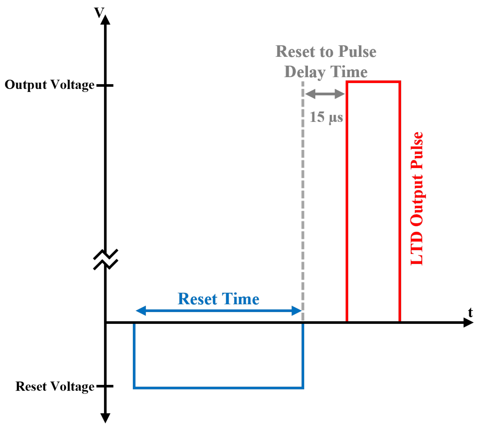
The 10-stage LTD was operated with charging voltages ranging from 100 V to kV and with the reset voltage set to 20 V. Output voltage diagnostics were collected using an in-house built voltage probe for voltages below 8 kV and a Northstar PVM-4 (North Star High Voltage, Bainbridge Island, WA, USA) for higher voltages. Current diagnostics were collected via a Pearson Model 2879 (Pearson Electronics, Palo Alto, CA, USA). All waveforms were recorded on a RIGOL DS7024 (RIGOL Technologies, Suzhou, China) with 2 GSa/s. Reset timing and initial triggers were generated with a Berkeley Nucleonics Corporation Model 575 trigger generator (Berkeley Nucleonics Corp., San Rafael, CA, USA). The reset pulse was applied, followed by a 15 μs delay before the main discharge trigger. All experiments were performed at room temperature. Core heating resulting from magnetic losses was not observed to be significant during testing, which is attributed to the low duty-cycle operating conditions employed.
Using magnetic core saturation to control pulse width causes the switch to conduct a very high current once the stage impedance collapses.
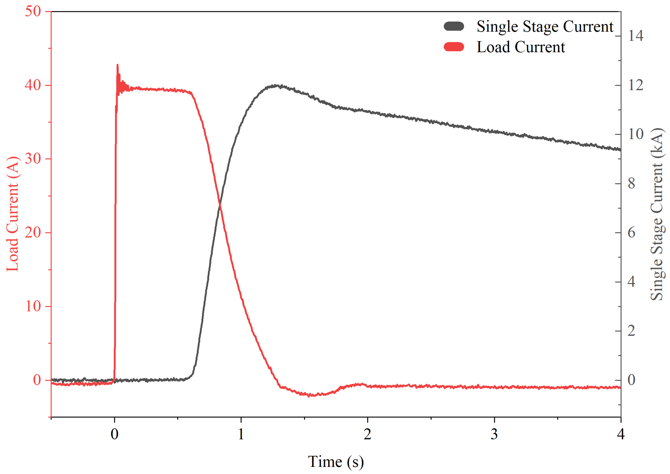
Figure 6 shows a representative waveform acquired during testing, showing both the output current and the current through the switches. As the core saturates and the stage impedance collapses, the current through the switch spikes rapidly, in this experiment peaking at 12 kA, while this peak current does not exceed the switch’s absolute maximum rating, the spike duration results in an
value higher than the switch’s rated limit. This current spike is the primary reason MOSFET switches are turned off before saturation occurs, as current at this level would destroy most other semiconductor switches utilized in LTD designs.
4.2. High Current Operation
One of the defining points of using thyristors is the ability to withstand high currents, enabling the ability for the LTD to drive lower impedance loads. To demonstrate the high-current capabilities of the thyristor-switched LTD, the system was operated without the current-limiting resistors by reducing the stage capacitance to an effective capacitance of
μF. This reduced capacitance allowed the thyristors to operate below the
threshold without requiring series resistance.
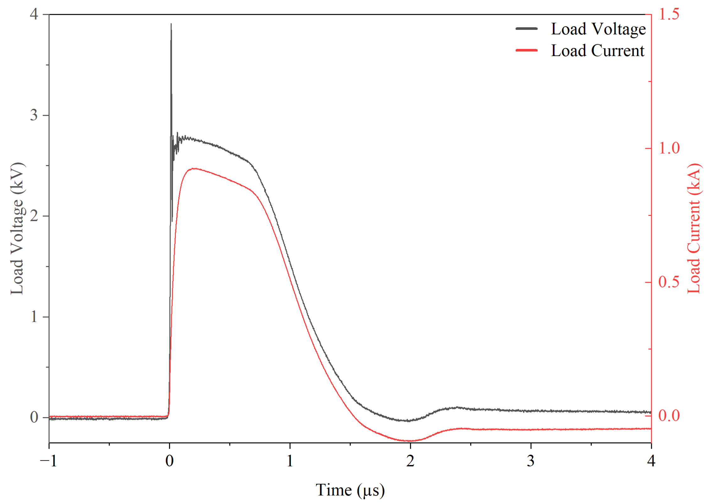
Figure 7 shows the output voltage and current waveforms for a 3-stage configuration driving a 3
load at 1 kV charging voltage. The device delivers a peak current of approximately 925 A to the load, corresponding to a peak power of
MW. This current level exceeds the per-stage current ratings typical of MOSFET-based LTD designs of comparable stage count [
11].
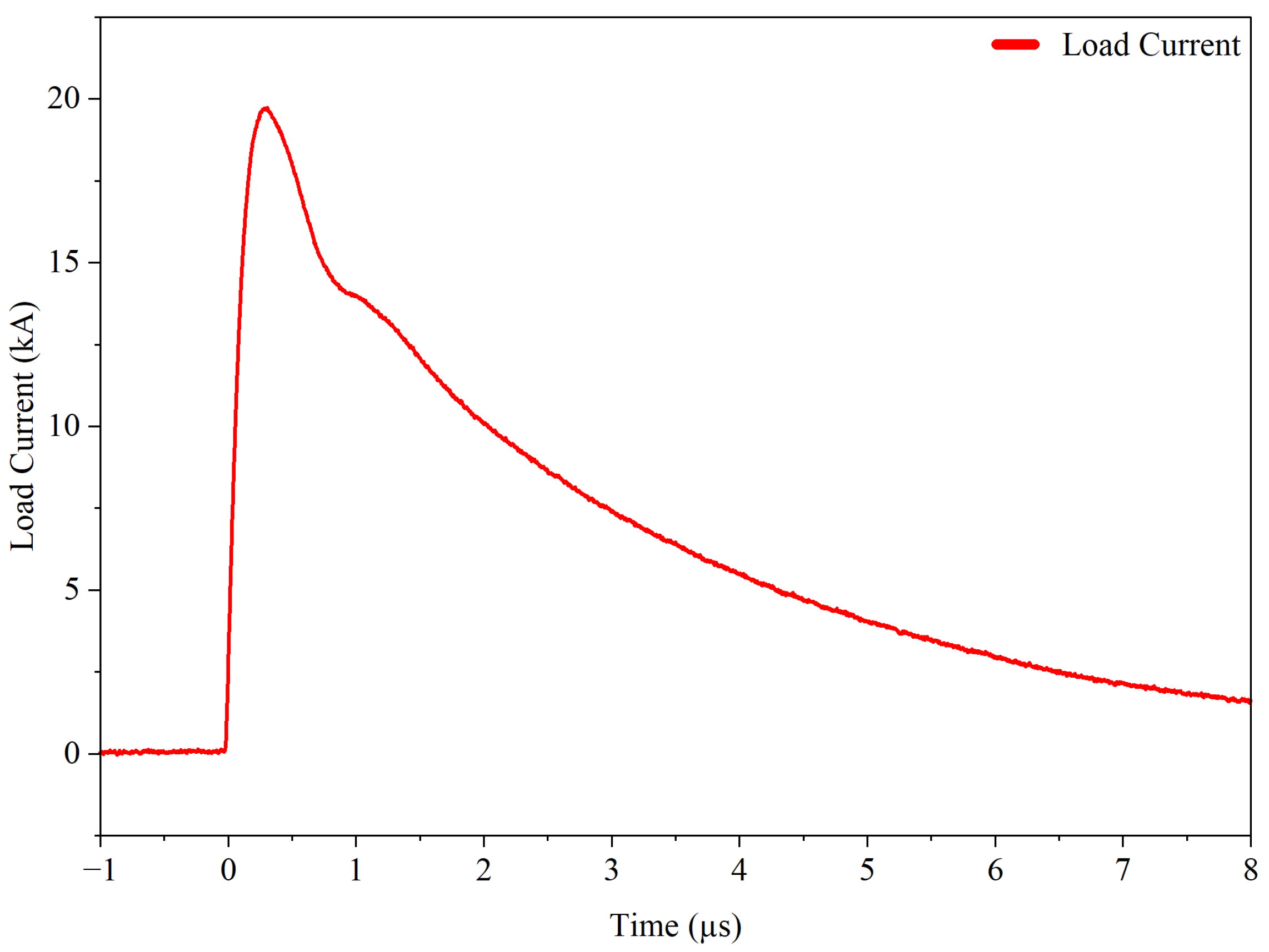
Further testing utilized a shorted load, roughly 23 nH, to demonstrate the peak current capability of the three-stage lower capacitance configuration.
Figure 8 shows the resulting output current waveform at
kV charging voltage. Under these conditions, the device delivered a peak current of approximately
kA. This corresponds to each switch experiencing a surge current of
kA. This per-switch current at the time applied is below the
threshold and resulted in no visible degradation to the switches when operated at this level.
With the full effective stage capacitance of 692 nF, the stored energy per stage reaches
J at
kV charging, producing post-saturation currents that greatly exceed the switch
rating, as shown in
Figure 6. In simulation, the inclusion of
reduces the peak saturation current from 12 kA to
kA, bringing the deposited
below the device rating. This is at the cost of the majority of the post-saturation energy dropping across the resistors rather than the switches and slightly lowering the amplitude of the output pulse. Reducing the stage capacitance to the values shown in
Figure 7 and
Figure 8 allows for the saturation current to remain within the
rating without the use of any series resistance. One should note, however, that a reduced capacitance will cause a considerable droop in the output voltage waveform at longer pulse durations for low-impedance loads. Alternatively, more switches could be paralleled per stage, which would allow further reduction of the series resistance. Ultimately, the design involves a trade-off between capacitance, switch count, circuit complexity, and desired pulse performance.
4.3. LTD Thyristor Pulse Width Modulation
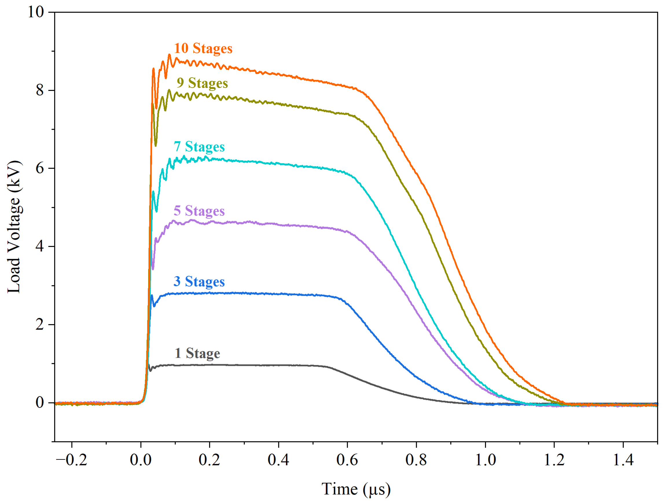
Figure 9 demonstrates the linear voltage addition as multiple stages are added to the device at 1 kV charging voltage. During this operation, a 500 μs reset pulse width was applied to the cores. Within this figure, waveforms are shown for various stage numbers, indicating that the LTD works as intended. The 10-stage output achieves approximately 8.9 kV peak voltage with a rise time of 15 ns. The current design of the board utilizes on-board resistors to limit peak current, extending the lifetime of the switches. These resistors introduce losses, resulting in a lower than expected voltage at the load.
By shifting the total reset time applied to each core at a constant charging voltage, the relationship between pulse width and reset time can be shown.
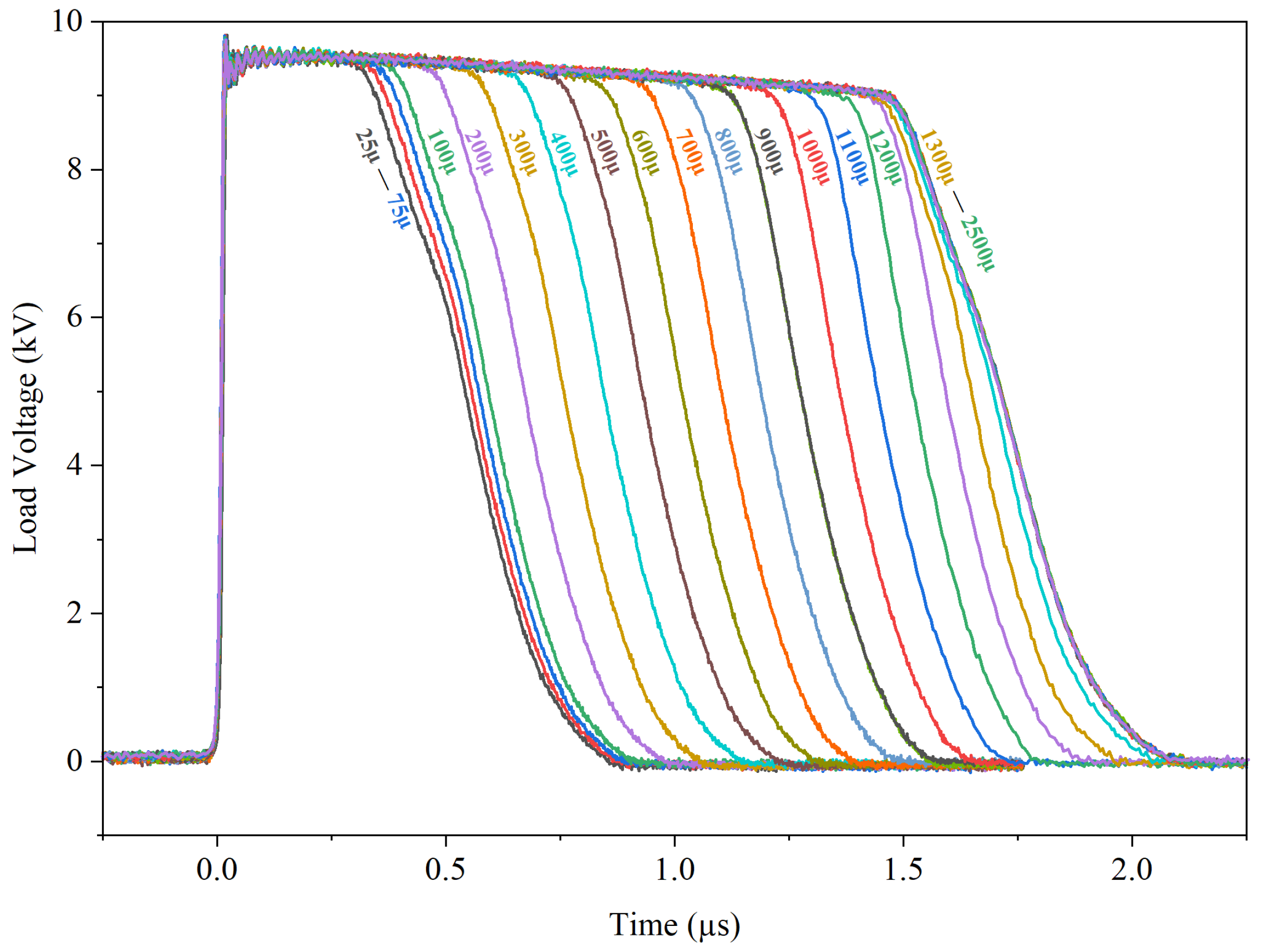
Figure 10 shows this relationship, with listed reset times next to each respective output signal. These were acquired using 10 stages, 1 kV charging voltage, and a 15 μs reset time to trigger pulse delay.
The shortest pulse width achieved is 538 ns at a reset time of 25 μs. The longest pulse width nears
μs, achieved with a reset time greater than
ms. This approaches our theoretical maximum of
μs calculated using Equation (
2). The slight discrepancy can be mainly attributed to unmodeled parasitics and the fact that the full voltage does not appear across the core. The pulse width, recorded as a function of applied reset time and analyzed in
Section 4.4, exhibits two regions that are expected. The first region is the linear region, existing from
s to
ms. In this region an increase in applied reset time results in an equally linear increase in the output pulse width. In the saturation/non-linear region longer pulses result in no increased pulse width. This relationship is expected and matches the behavior of magnetization in magnetic cores and Equation (
2).
Across the full reset-time sweep shown in
Figure 10, the peak output amplitude remained stable at approximately
kV with a standard deviation of
V across all reset settings. This indicates that the reset state of the magnetic cores controls the pulse duration without significantly affecting the delivered voltage amplitude.
As discussed in
Section 2, the minimum pulse length depends not only on the saturation point but also on the reset-to-trigger delay. As the inter-pulse spacing decreases, the core has less time to relax back to the remanent point. As such the linear portion of this region continues until reset times smaller than 25 μs, and will continue in linear fashion until
. Pulses shorter than
require that the core is biased to a point between
and
. This requires a reset pulse of inverted amplitude compared to the reset pulses utilized to drive the core to below
normally.
While experimental verification of sub-500 ns operation was not performed, the achievable range can be estimated from Equation (
2). In principle, as
approaches
, the available flux swing
approaches zero, and the pulse width is bounded only by the output rise time. Using the parameters of
Figure 10 fit (
= 975 V,
=
cm
2), biasing the core to
T would yield a predicted width of 289 ns, and biasing to 1 T would yield 140 ns. In practice, three main factors establish a floor much greater than the LTD rise time of 15 ns. The first is the quality of the pulse; as
decreases, the saturated portion of the falling edge occupies a larger fraction of the total pulse. This will degrade the flat top before a true square pulse is formed. The second limitation is timing precision. There is a finite delay between the reset pulse and the LTD output pulse. To implement this technique effectively, that delay must be both short and highly repeatable to ensure that the core does not relax back toward
before the main pulse arrives. The final requirement is an inverted-polarity reset drive, while the unipolar reset boards used in this work cannot bias the core beyond
in the required direction; extension of the tunable pulse-duration range into the 100–500 ns regime is readily achievable through the use of a bipolar reset supply combined with tighter trigger-timing control.
4.4. Pulse Width Fitting
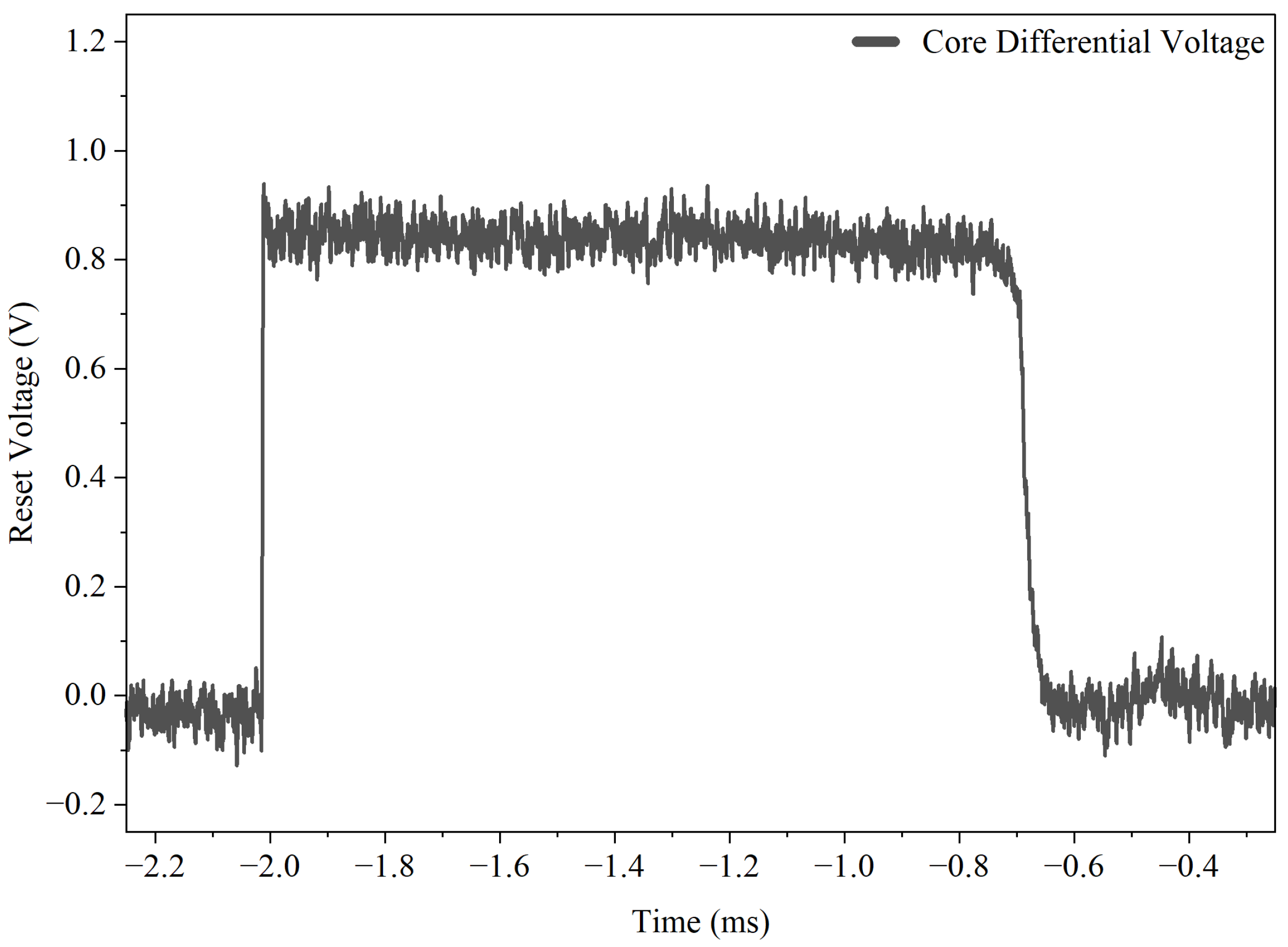
Matching the magnetic core’s response to the relationship between output pulse width and reset time requires consideration of several factors. During testing, it was found that a reset pulse of
V was physically applied to the core. The reduction from the 20 V capacitor charge voltage to the measured
V is a consequence of the board’s output impedance. The current-limiting resistor,
, is the dominant impedance on the discharge path with a value of 4
. With the added 1
switch resistance, the unsaturated core presents a relatively low impedance at the timescale of interest. As a result, most of the source voltage is dropped across
and the switch, leaving approximately
V across the winding. This divider behavior is stable over the entire reset duration, as indicated by the flat top present in
Figure 11, so the volt-second product delivered to the core remains linear with
and Equation (
3) remains valid. The energy cost of the reset process can be found to be 104 mJ, with the core needing
mJ to reach
. The resistance of
was set such that the core current would be 4 A; lowering this resistance would apply a higher voltage to the core and increase the speed at which the core reset would take place. For a voltage of
V, it was found that if a reset pulse was applied for longer than
ms, the core would reach
, as shown in
Figure 11. Within this figure, saturation can be seen to occur at approximately
μs. As a result, any increase in reset pulse width beyond
ms would result in no increase in overall pulse width.
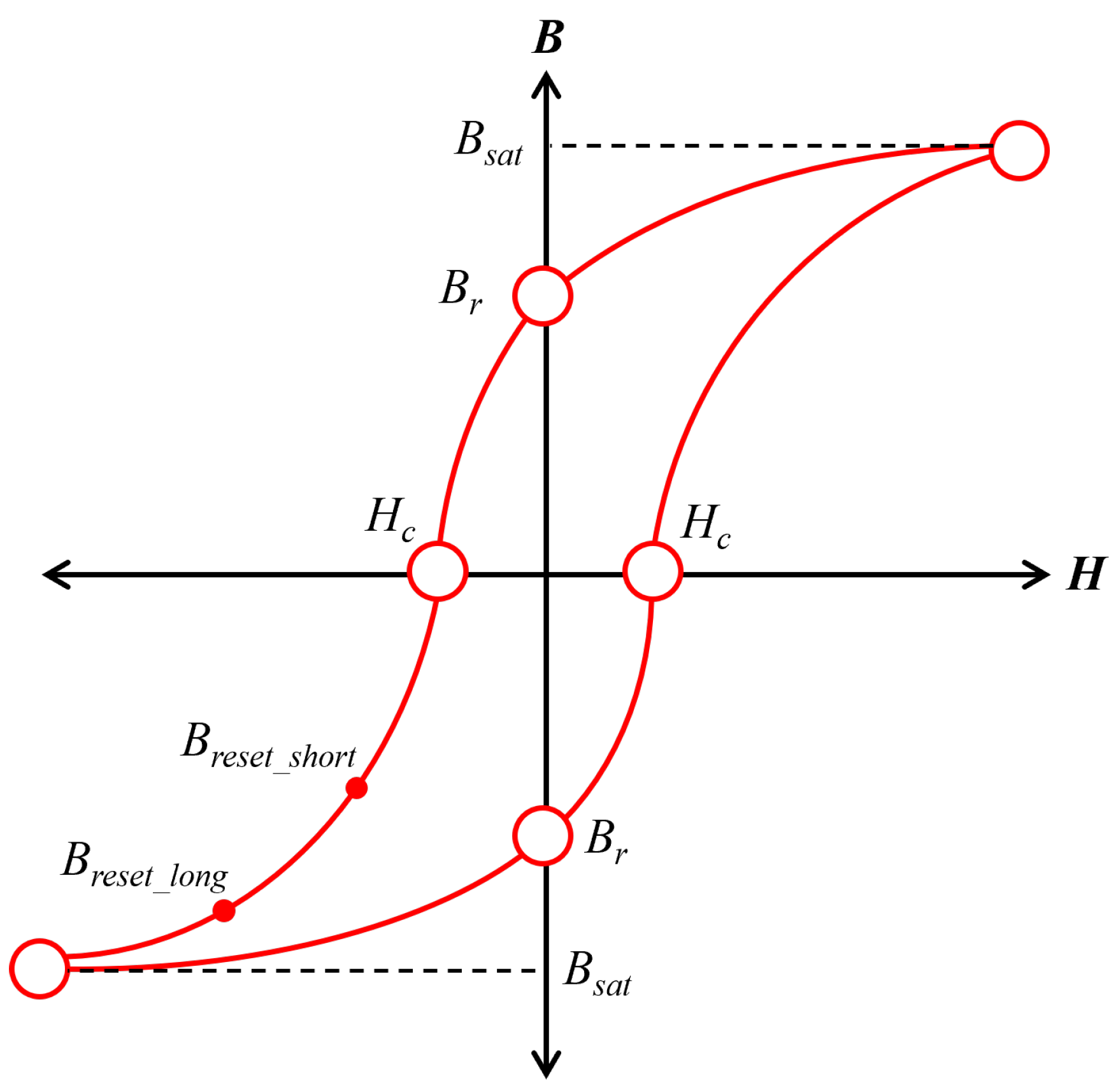
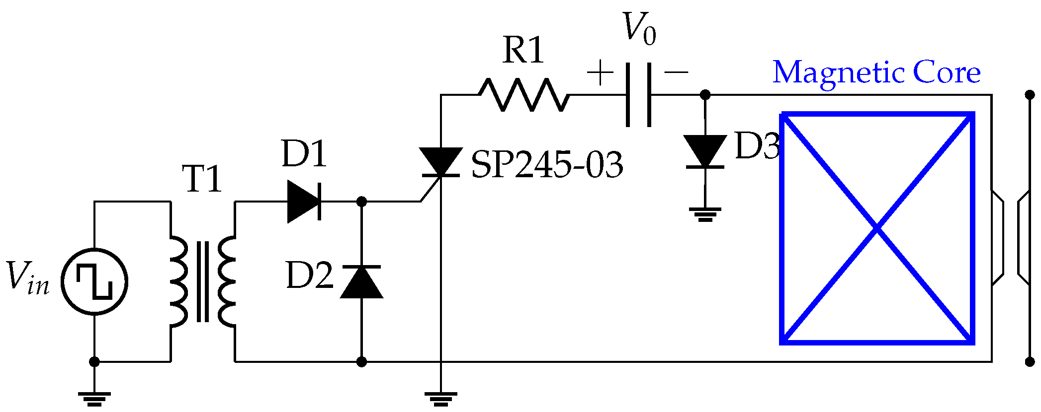
During testing and analysis of experimental results, it was found that the remanent flux density did not match the expected levels from the manufacturer datasheet. After saturation, the collapsing field induces a negative voltage transient that forward-biases the diode, shunting the remaining capacitor energy while providing a small reverse current that resets the core’s operating point to below the remanent flux density. As a result, the post-pulse operating point becomes:
where
is
T according to the manufacturer datasheet for the magnetic material [
14]. The value of
can be determined by integrating the reverse voltage experienced by the core.
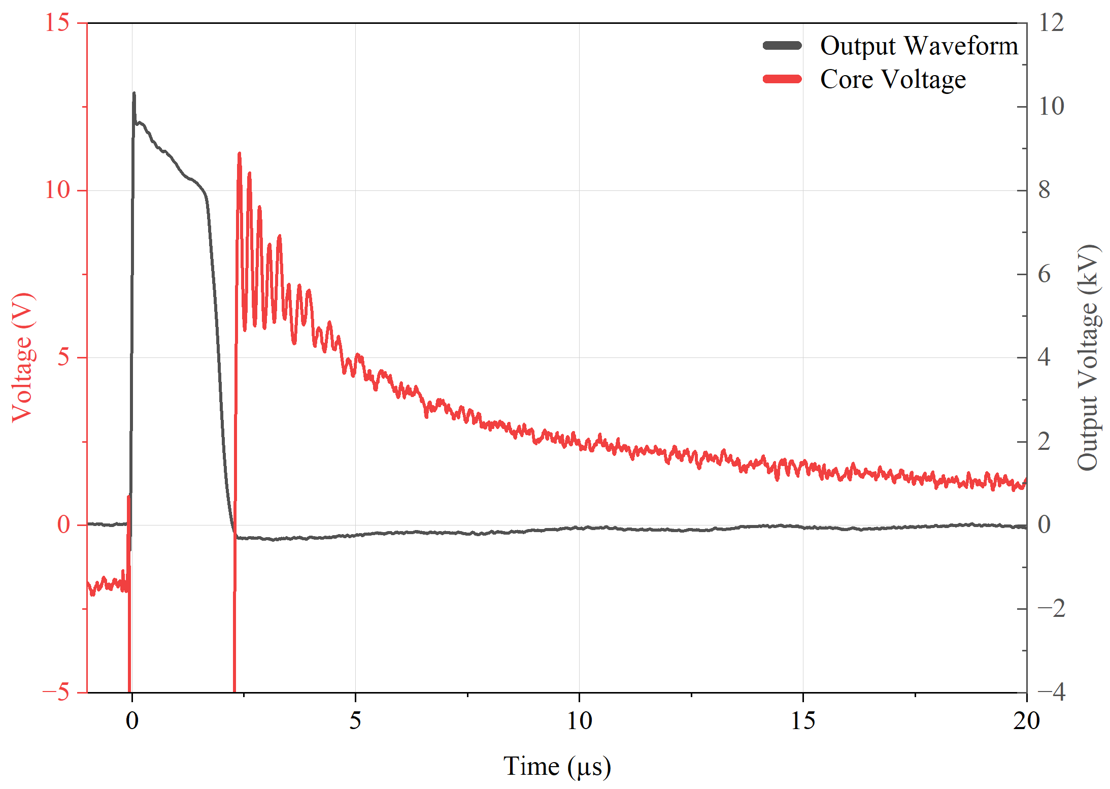
Figure 12 displays both the output pulse and the voltage across the magnetic core. As the output voltage collapses, the core experiences a voltage transient, resulting in a shift in the core’s operating point. For the 10
load case, integration of the post-pulse voltage reversal across the core yields a reverse flux density change of 0.113 T, resulting in an effective pulse operating point of
T using Equation (
5). When operating with the 50
load, the higher load impedance results in a greater fraction of the supply voltage appearing across the core during the voltage reversal, producing a correspondingly greater reverse flux swing. Direct measurement of the 50
reversal transient was not performed in this configuration. However, fitting Equation (
2) to the experimentally measured pulse widths shown in
Figure 13 yielded an effective post-pulse operating point of
T, corresponding to a reverse flux change of 0.17 T. This value is consistent with the expected increase in reverse swing and shows good agreement with the experimental pulse width data across the full linear region. The deviation of the post-pulse operating point is consistent with the permeability behavior observed during excitation reversals in magnetic cores. Wan et al. demonstrates this effect through a Preisach-based hysteresis model of LTD, in which the core’s permeability decreases sharply when the excitation direction reverses, causing the flux to follow a first-order reversal curve rather than the main B-H loop [
15]. This behavior results in the post-transient operating point differing from the specified datasheet values. Additionally, recent work by Kelp et al. on modeling pulsed magnetic core behavior has shown that traditional circuit models fail to capture the magnetization-rate-dependent response of nanocrystalline cores under pulsed operation, further supporting the need for empirical parameter extraction in situations such as these [
16].
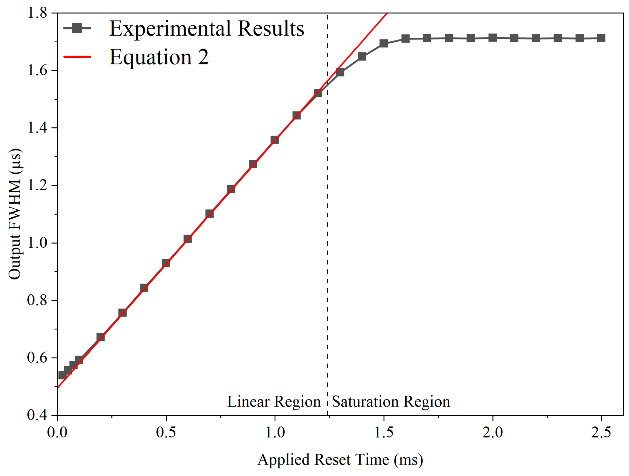
Figure 13 plots the measured pulse widths from
Figure 10 and compares them against the theoretical predictions from Equation (
2). Two distinct regions are evident in this graph: a linear region before saturation occurs on the reset and a region post-saturation. The linear section allows for direct increases in reset duration to result in an equal increase in pulse width, determined by Equation (
2). This region shows good matching with results from Equation (
2). Beyond this point the LTD reaches its maximum possible pulse length due to reaching the maximum flux swing found in Equation (
4). Shorter pulses are also possible but require biasing the core in the opposite direction prior to the output pulse, but that was unexplored in this work.
Although the pulse-width sweep of
Figure 10 was acquired with the 50
load, the voltage scaling predicted by Equation (
2) can be validated against the 10
data of
Figure 9, where approximately 900 V appear, across each core. For the 500 μs reset applied during the experiment, Equation (
3) yields
T. Together with the measured operating point of
T, this corresponds to a flux swing of
T, equivalent to a volt-second capacity of 858 V · μs. Integrating the measured ten-stage output waveform from turn-on to saturation results in 723 V · μs per stage, corresponding to a flux swing of
T. The discrepancy is largely attributable to the pronounced voltage droop observed with the 10
load. Unlike the nearly flat-topped pulses obtained with the 50
load, the 10
waveform does not maintain a constant voltage throughout the pulse, making the measured FWHM of 852 ns a conservative estimate of the actual saturation-limited pulse duration.




 ,
,