3.1. Simulation Analysis
To verify the operating characteristics of the high-voltage power supply for the electron curtain accelerator, a simulation model of the high-voltage charging power supply system was established using PSIM and MATLAB/Simulink. The simulation parameters were configured as follows: three-phase input voltage of 380 V, switching frequency of 15 kHz, resonant inductance of 52.8 μH, resonant capacitance of 0.3 μF, and resonant frequency of 40 kHz. These parameters satisfy the soft-switching condition, i.e., fs ≤ 0.5fr. The transformer turns ratio is 1:192, the load capacitance is 0.1 μF, and the simulation duration is 500 ms.
The number of switching cycles (m) at the end of charging can be obtained by substituting the above parameters into Equation (1):
With
m = 1536, substituting into Equation (2) gives the maximum resonant current:
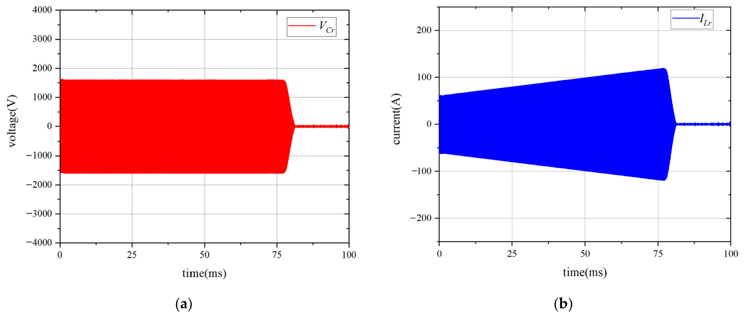
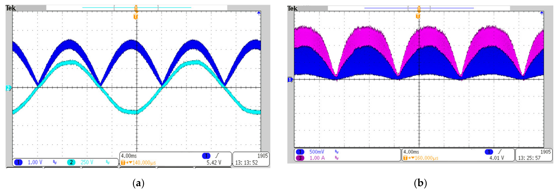
The voltage envelope waveform across the resonant capacitor is shown in
Figure 12a and is consistent with the theoretical calculations. The resonant current envelope waveform is shown in
Figure 12b, with a peak value of approximately 118.75 A, which is close to the theoretical value.
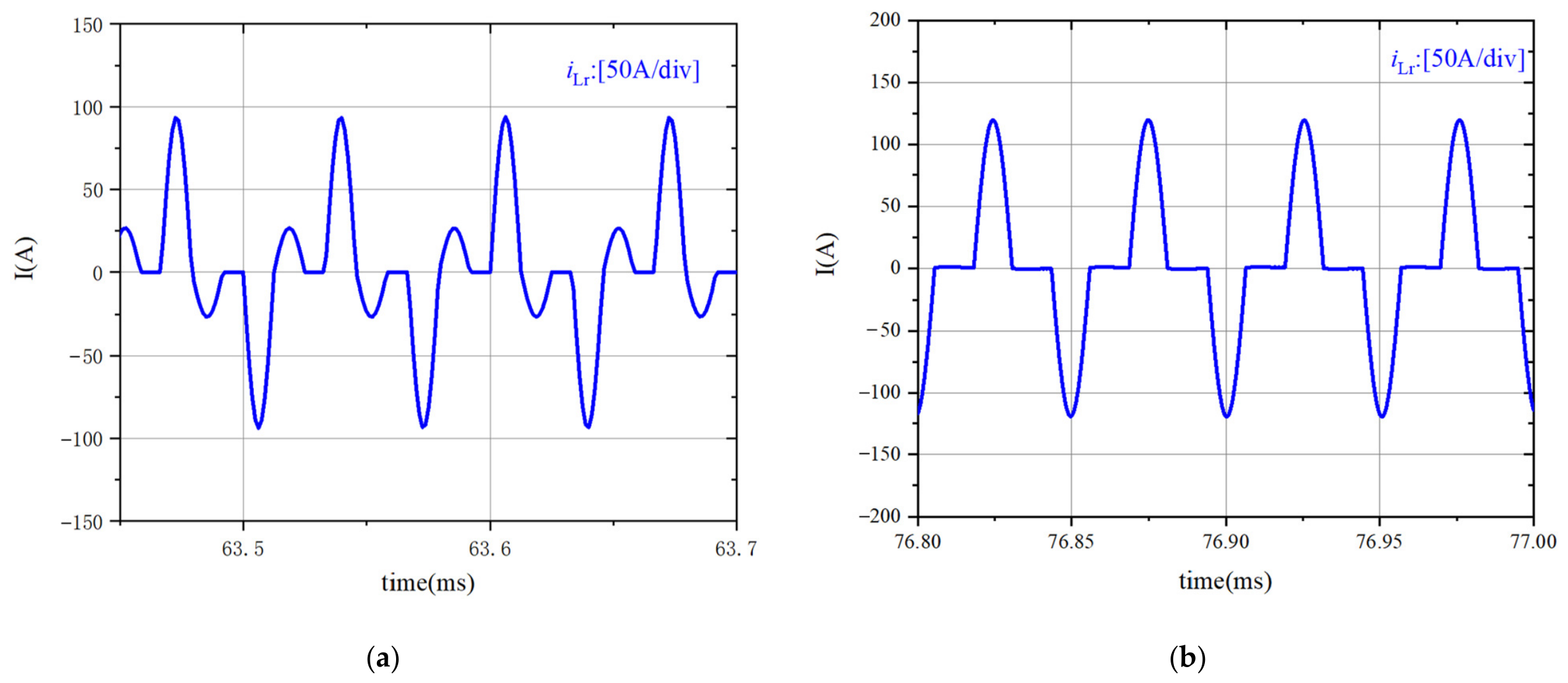
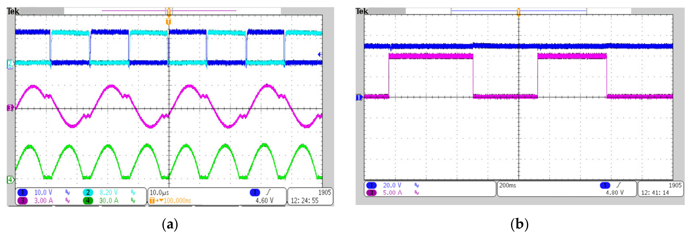
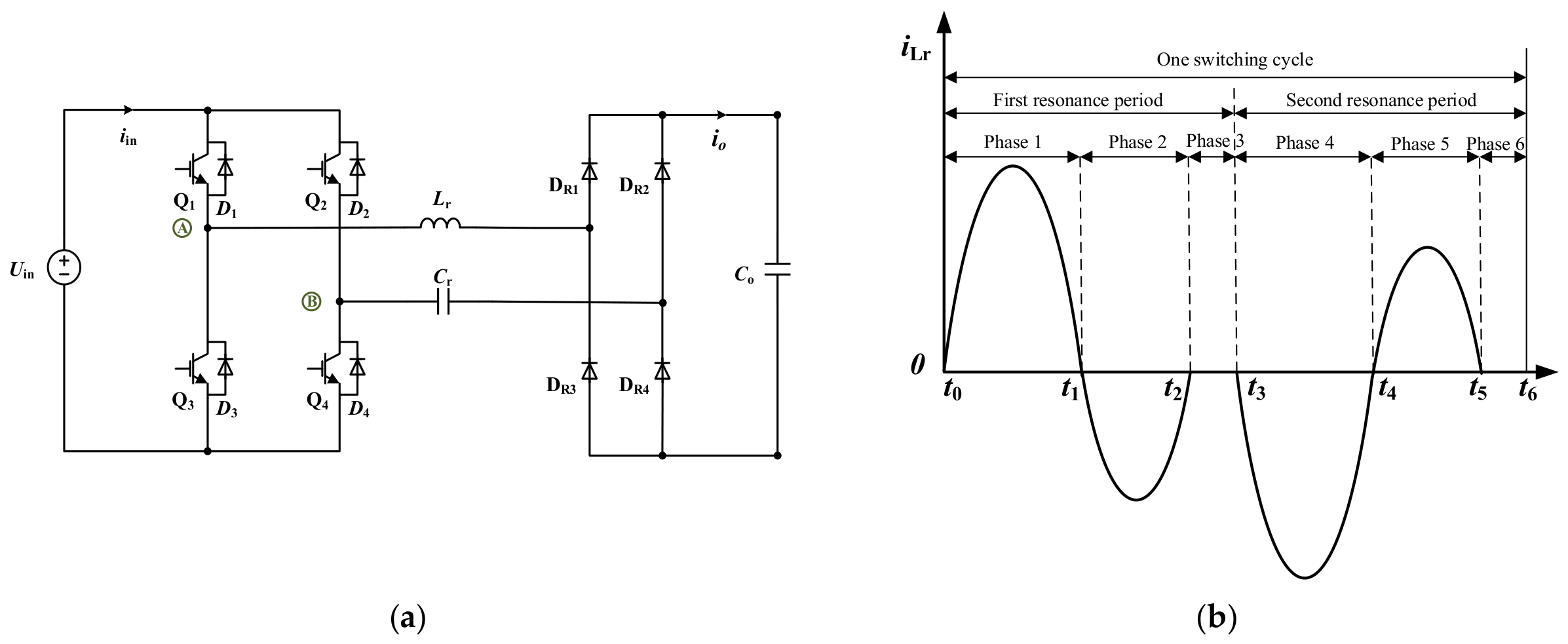
Upon magnifying and examining the resonant current waveform, the charging process revealed two sequential phases: a linear phase followed by a nonlinear phase. Initially, as shown in
Figure 13a, the system is in the linear charging stage, during which the peak resonant current increases linearly while the average value remains constant. In this stage, the current is discontinuous, and the inverter bridge operates in soft-switching mode. As the peak current is reached, the charging process transitions smoothly into the nonlinear stage, as shown in
Figure 13b, where the resonant current gradually decays and the current through the freewheeling diodes drops to zero.
The load voltage waveform is shown in
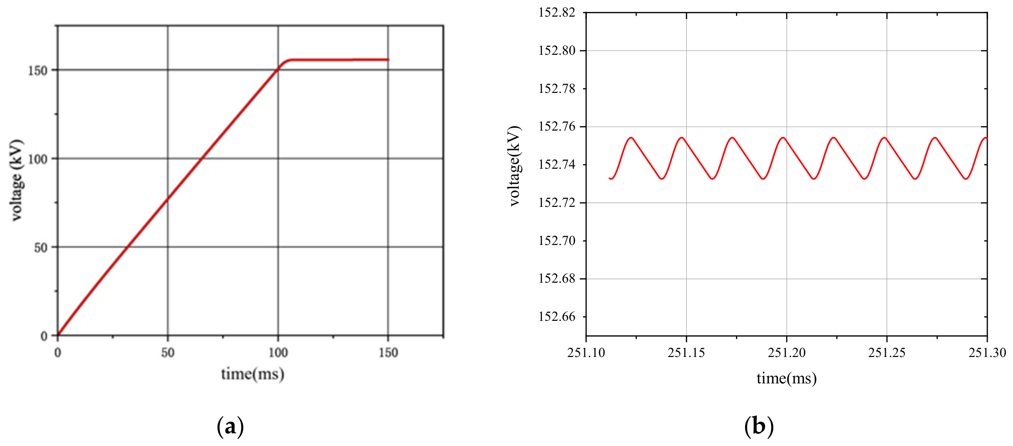
Figure 14a. As shown in the figure, the charging voltage increases linearly, while the charging current remains essentially constant. At a switching frequency of 15 kHz, the charging time is approximately 102.4 ms, and the output voltage stabilizes at around 155.7 kV. As shown in
Figure 14b, under rated load conditions, the output voltage ripple is approximately 24 V, with a ripple rate of about 0.01%, meeting the design specifications.
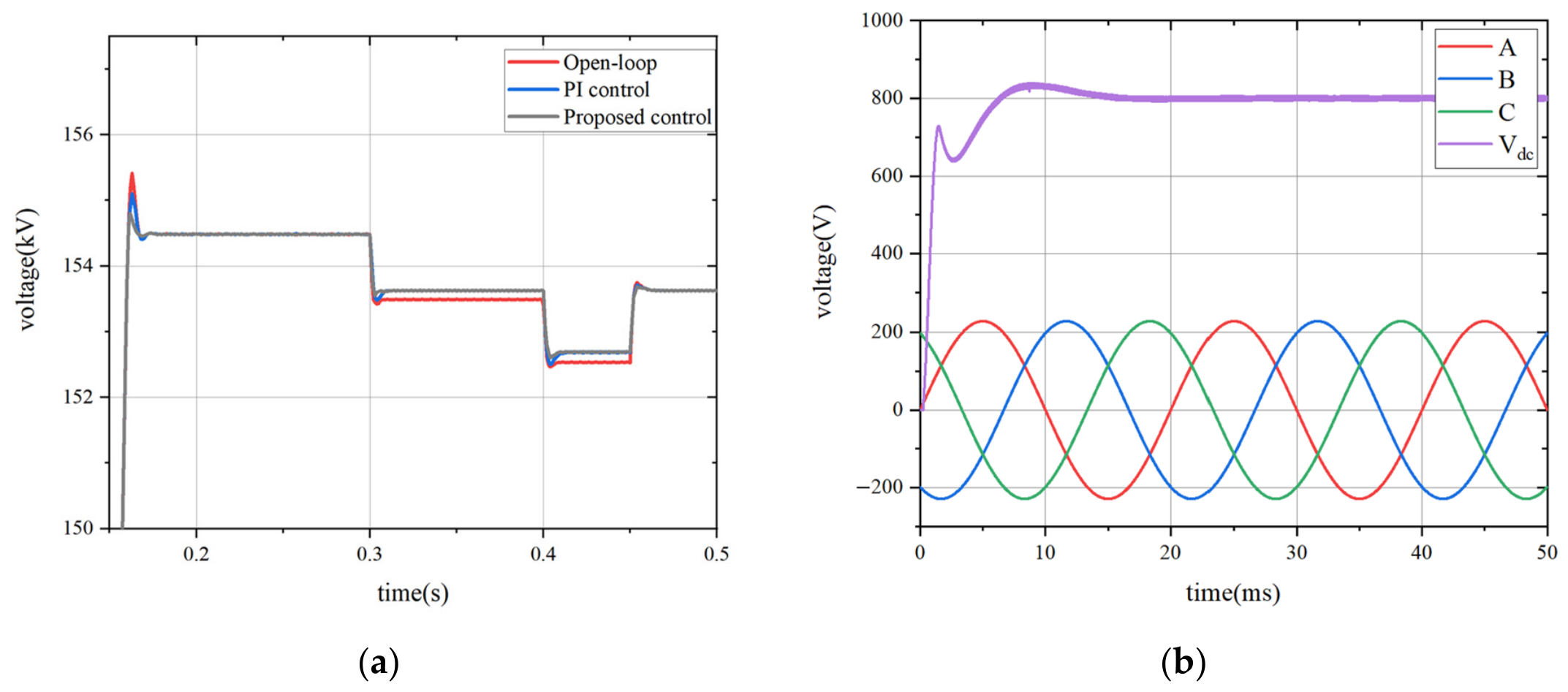
The PFC control system designed in this paper comprises three components: dual-loop voltage and current control, an adaptive lookup table-based digital phase-locked loop, and grid voltage feedforward compensation. Each component has been optimized to address the shortcomings of conventional control schemes. To verify the dynamic performance of the control system designed in this paper, a simulation platform was established to compare three control schemes: open-loop control, conventional single-voltage-loop PI control, and the complete PFC control system described herein. The simulation was set up to simulate a light-load startup with sudden load changes; the load variation conditions are shown in
Figure 15a. During the system startup phase, the voltage overshoot in the open-loop state was approximately 0.9 kV; under conventional PI control, the overshoot was suppressed to 0.6 kV, while under the control scheme proposed in this paper, the overshoot was only 0.3 kV, and the voltage quickly stabilized near the rated value. At 0.3 s, a sudden load increase disturbance was applied, switching the load from light load to rated load. At this point, the voltage drop under open-loop control reaches 1.3 kV, and due to the lack of closed-loop regulation capability, the voltage cannot recover to its original steady-state value; under conventional PI control, the voltage drop is 1.1 kV, and it returns to the steady-state approximately 80 ms later. The voltage drop under the control method described in this paper was the smallest, at only 1.0 kV, and the recovery speed was the fastest, returning to the steady-state value in approximately 50 ms, with a relative load regulation rate of about 0.65%. At t = 0.4 s, the load was further increased to an overloaded state; the voltage under open-loop control dropped significantly further, and the steady-state voltage remained persistently low. Conventional PI control exhibited a voltage drop of 0.7 kV with a slower recovery rate; the control method described in this paper resulted in a voltage drop of only 0.6 kV and reached a new steady state in approximately 40 ms, maintaining good regulation capability even under overload conditions and avoiding severe voltage fluctuations. This demonstrates that the control system designed in this paper possesses excellent voltage stability and disturbance rejection capability under load disturbances, meeting the system’s dynamic design requirements.
Assume that the grid voltage fluctuates within ±10%. Observe whether the SPWM rectified output voltage stays near 800 V.
Figure 15b shows that when the grid voltage drops by 10%, the output DC voltage briefly overshoots, then quickly stabilizes at about 800 V. The closed-loop feedback remains effective, with relative line regulation of about 0.01%, meeting the requirements.
Building on the simulation of the main circuit’s electrical characteristics, this paper further conducted three-dimensional electrostatic field simulations of the transformer and simulations of the high-voltage system. It quantitatively verified the core performance of the system at a rated voltage of 150 kV, providing comprehensive theoretical support for the engineering feasibility of the design scheme.
First, an electrostatic field analysis of the transformer was performed using COMSOL Multiphysics 6.2 software to verify its insulation performance under 150 kV operating conditions.
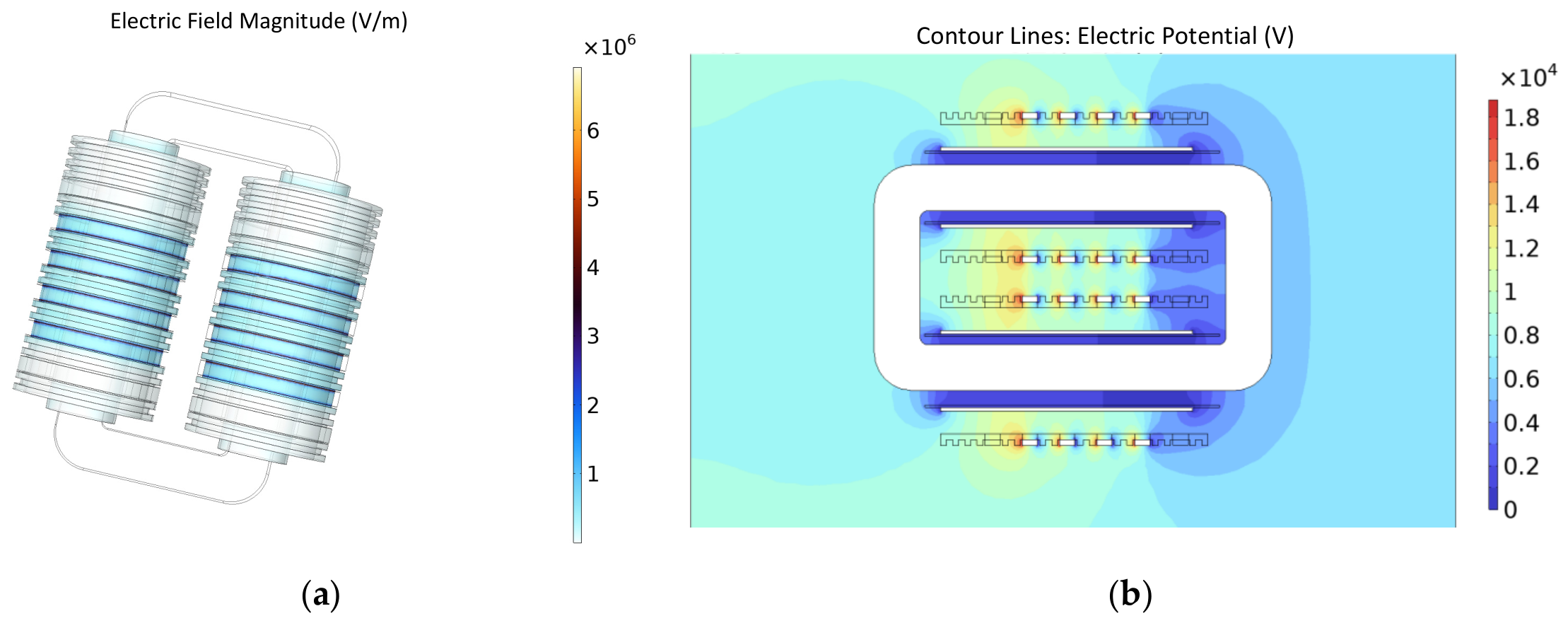
Figure 16a,b respectively shows the overall electric field cloud map and the electric potential contour map of the transformer under 150 kV operating conditions.
Simulation results indicate that the maximum electric field strength is approximately 9.87 kV/mm, primarily concentrated at the edges of the windings and in areas with high local curvature. Since the system employs an oil-immersed insulation structure with a breakdown field strength exceeding 15 kV/mm, the current maximum field strength remains below the dielectric strength limit of the insulation medium. The results demonstrate that the designed structure is feasible for high-voltage insulation.
The parasitic parameters between the transformer windings were extracted using the Maxwell capacitance matrix, as shown in
Table 6.
In this context, C11 and C22 represent the parasitic capacitance of each winding to ground, while C12 and C21 represent the mutual parasitic capacitance between windings, reflecting the electric field coupling between the series-connected secondary windings.
Lower mutual capacitance helps reduce dynamic voltage coupling between high-voltage windings, thereby improving the voltage balancing performance of series windings and reducing the risk of local voltage overshoot. Meanwhile, an accurate assessment of parasitic capacitance to ground provides a direct basis for high-voltage insulation design and winding arrangement optimization, effectively controlling parasitic current paths and reducing the risk of leakage current and partial discharge.
In addition, the magnetic coupling characteristics of the transformer were analyzed using the COMSOL magnetic field module. The simulation results indicate that the proposed multi-winding structure exhibits good magnetic coupling behavior with limited leakage flux distribution.
Under high-voltage pulse operating conditions, no significant voltage oscillation or local overvoltage phenomenon was observed in the simulation results, indicating that the influence of transformer leakage inductance is effectively suppressed within the designed operating range.
At the same time, typical operating conditions were simulated using PSIM software to extract the output voltages of the eight secondary rectifier units and calculate the voltage unevenness coefficient.
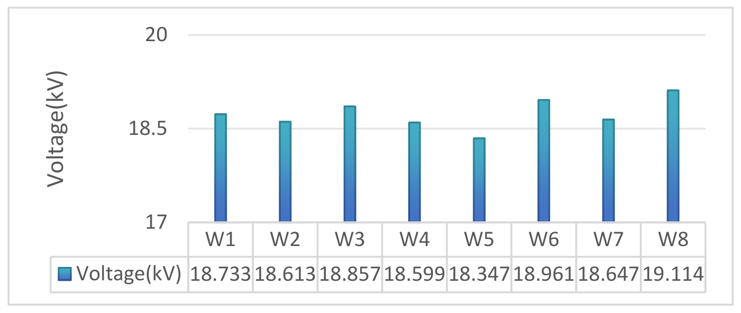
The voltages of the eight windings are shown in
Figure 17.
The results show that the voltages across the windings stabilized between 18.3 and 19.1 kV, the unevenness coefficient decreased to 1.02, and the deviation was kept within 3%, meeting the design requirements. This indicates that the proposed structure possesses good high-voltage equalization capabilities and can effectively reduce the risk of local winding overvoltage.
3.2. High-Voltage Power Supply Testing
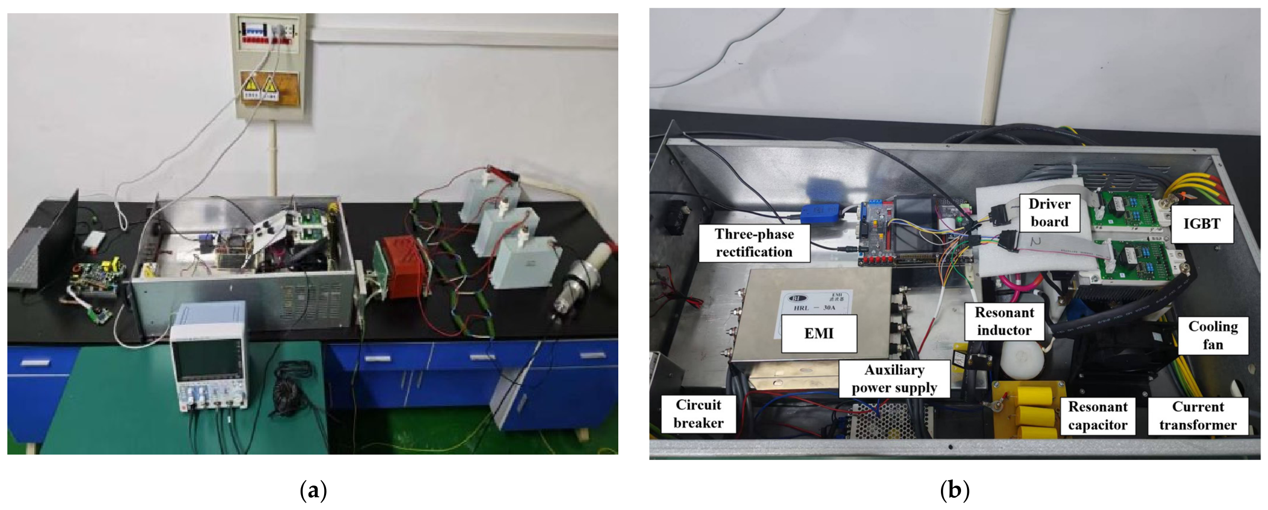
A low-voltage proof-of-concept experimental platform was established to test the operational performance of the power supply prototype, as shown in
Figure 18a,b. This platform uses high-frequency transformers already available in the laboratory for testing. The experiment verified resonance charging behavior, soft-switching operation, and the closed-loop control algorithm. The dedicated 150 kV high-voltage transformer designed in this paper was not included in the experiment due to manufacturing and assembly lead times.
The key component parameters of the experimental platform are summarized in
Table 7. The system consists of an AC input EMI filtering stage, a high-power switching stage based on IGBTs, an LC resonant energy conversion stage, a step-up transformer, a high-voltage rectifier load, and a digital control unit implemented by an FPGA.
To ensure safe and reliable operation, thermal protection is applied to major heat-generating components. The load and measurement systems are configured to emulate practical high-voltage operating conditions and ensure accurate waveform acquisition.
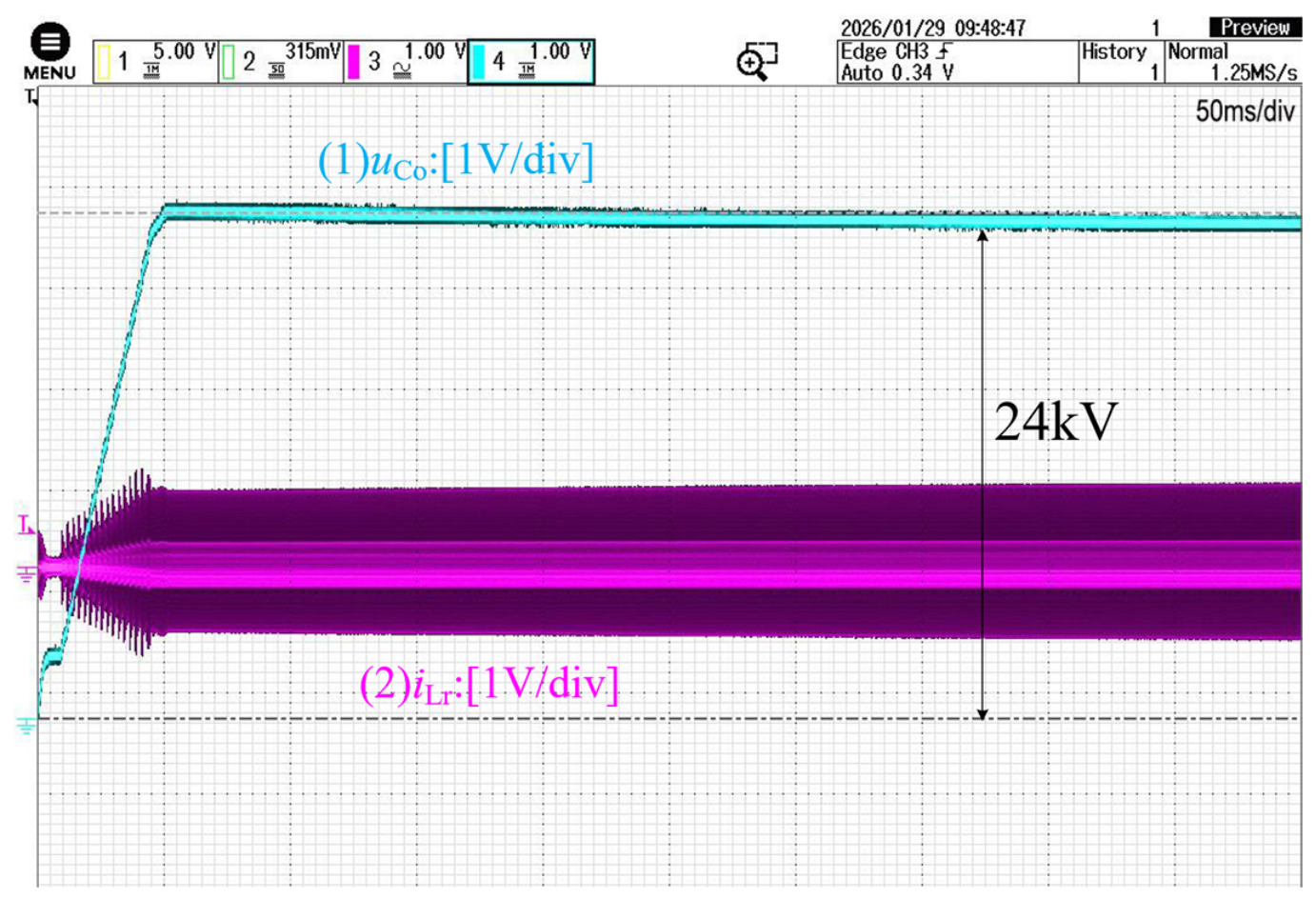
With the DC input voltage set to 800 V and the switching frequency to 15 kHz, a no-load charging test was conducted. The results are shown in
Figure 19. The platform achieved a maximum output voltage of 24 kV, with a charging time of approximately 50 ms. The slope of the load voltage rise was stable, indicating that the charging current was approximately constant; thus, this can be considered constant-current charging.
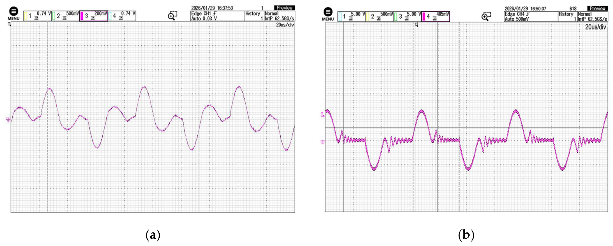
Load tests were conducted using a 60 kΩ load to observe the resonant current waveform.
Figure 20a below shows the waveform during the early stage of resonant charging, while
Figure 20b shows the waveform during the late stage of resonant charging. During the early charging stage, the current exhibits discontinuities, and the inverter bridge operates in soft-switching mode. Due to the transformer’s distributed capacitance, the current waveform shows slight oscillations compared to the simulation, but the resonant period generally matches the switching period. As charging nears completion and the output voltage gradually increases, the amplitude of the resonant current decreases. The inverter bridge continues to operate in soft-switching mode without hard-switching transients; minor high-frequency oscillations caused by parasitic parameters on the load side do not affect system stability. Test results show a peak resonant current of approximately 40 A and a load current of approximately 0.4 A, corresponding to an output power of approximately 9.6 kW. The calculated power supply efficiency is 96%, meeting the design specifications.
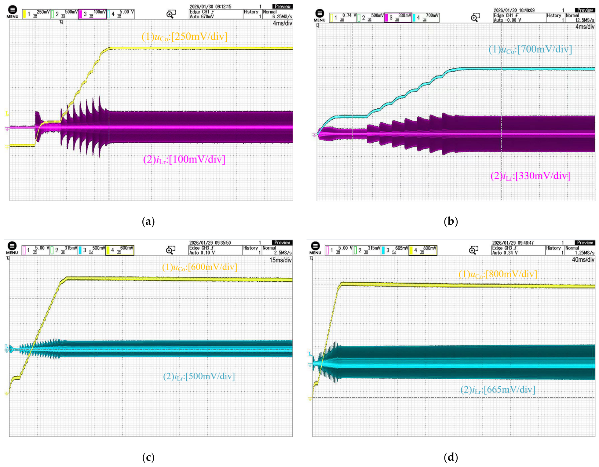
Closed-loop voltage regulation tests were conducted on the prototype. Charging voltage waveforms at 5 kV, 10 kV, 15 kV, and 20 kV are shown in
Figure 21a–d. The load voltage rises smoothly. The charging current remains stable. The charging time is nearly proportional to the set voltage. The closed-loop system continuously monitors output voltage and adjusts the switching frequency to maintain the set value. This validates the effectiveness of the feedback loop.
Table 8 shows the slope of the voltage rise at different charging voltages.
As shown in the table, under operating conditions with different target voltages, the system’s voltage rise rate remains stable at approximately 625 V/ms, with relative fluctuations strictly limited to within ±1.5%. This indicates that the digital closed-loop control system is capable of precisely maintaining a constant average charging current during the initial phase across different charging targets. Toward the end of the charging process, as the voltage approaches the setpoint, the current naturally enters a nonlinear decay phase due to the physical characteristics of the topology; however, the constant-current performance during the core charging interval is fully supported by cross-condition validation.
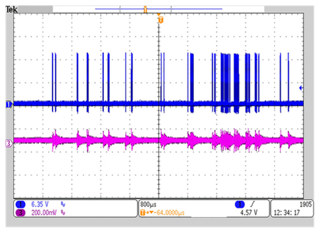
Figure 22 shows the waveform diagram of the output ripple and the hysteresis control flag. Specifically, the output ripple is approximately 25 V, while the burst control flag fluctuates around the set trigger voltage of 24 kV. As a result, voltage accuracy is maintained at around 0.1%. The hysteresis control circuit thereby stabilizes fluctuations near the set voltage, helping maintain a steady output and enabling the system to meet the accuracy requirements of high-voltage charging power supplies.