Article

A Self-Powered, Fast-Response High-Voltage Safety Discharge Topology Based on Cascaded Depletion-Mode NMOS for Compact Pulse Generators

1
School of Mechanical and Electrical Engineering, North University of China, Taiyuan 030051, China
2
School of Mechatronical Engineering, Beijing Institute of Technology, Beijing 100081, China
3
Yangtze Delta Region Academy in Jiaxing, Beijing Institute of Technology, Jiaxing 314019, China
*
Author to whom correspondence should be addressed.
Electronics 2026, 15(11), 2346; https://doi.org/10.3390/electronics15112346
Submission received: 22 April 2026 / Revised: 22 May 2026 / Accepted: 26 May 2026 / Published: 28 May 2026
(This article belongs to the Section Power Electronics)

Abstract

High-voltage short pulse generators play a critical role in medical and industrial applications. However, the presence of residual stored energy can pose significant electrical safety hazards. To mitigate these hazards, the implementation of rapid discharge mechanisms is imperative. To address the limitations of slow passive bleeders and auxiliary-dependent active circuits, and the issue of excessive size for compact pulse generators, this study proposes a self-powered, fast-response discharge topology utilizing cascaded depletion-mode NMOS transistors. The method utilizes the inherent normally-on characteristic of depletion-mode devices to ensure fail-safe activation during power loss, employing a self-biased feedback loop to regulate a constant discharge current. The theoretical models were validated through simulations and a hardware prototype testing a 1200 V/220 nF capacitor. The experimental results demonstrate the capability to successfully discharge 1200 V to a safe level within a span of one second. Additionally, the discharge time can be programmed within the range from 72 milliseconds to 1.02 s by adjusting the current-limiting resistor. In summary, the proposed topology offers a reliable, compact, and adjustable solution for high-voltage safety, addressing the limitations of conventional discharge technologies in terms of volume and speed.

1. Introduction

The short pulse generator has the capacity to convert long-term low-power input into short-term high-power output, characterized by high voltage, high current, and fast rise time. It is capable of generating single shot or periodic high-voltage pulses [1,2,3,4].
Short pulse generators have found diverse applications across various high-impact fields. In the medical domain, these generators are widely used in electroporation, a technique that involves the application of short electric pulses to enhance the permeability of cell membranes, facilitating drug delivery and gene therapy [5,6]. Furthermore, short-pulse generators have been demonstrated to play a crucial role in the generation of plasma, where they facilitate the creation of high-energy plasma states that are necessary for a variety of applications in material processing and surface modification [2,7]. The high-voltage, rapid-pulse characteristics of these generators facilitate more efficient plasma formation, thereby enhancing the performance of industrial systems [8]. In the industrial sector, they are integral to ignition systems, where their ability to generate precise, high-energy pulses ensures reliable combustion [4]. In the domain of defense, short pulse generators play a pivotal role in the development of sophisticated weapon systems, encompassing electromagnetic weapons and directed-energy devices. These generators facilitate the generation of high-powered electromagnetic pulses with the potential to disable electronic systems or modify the functionality of enemy devices [9,10]. Driven by the growing demand for compact and integrated systems across these diverse applications, miniaturizing high-voltage pulse generators has become a key area of research [11,12,13]. Traditionally, these generators relied on bulky gas-based switches and large-scale capacitor banks, which limited their use in environments with space constraints. Recent research has primarily focused on overcoming these limitations through a multi-pronged strategy. One significant trend is the shift from conventional spark gaps to robust, all-solid-state switching architectures that leverage the superior performance of devices such as SiC, MOSFET and IGBT [11,14,15,16]. These solid-state switches offer exceptional reliability, precise jitter control, and crucially, the potential for monolithic integration. Concurrently, innovations in passive component technology are being actively pursued. This includes developing compact, high-energy-density dielectric materials for pulse forming networks, such as advanced polymer films and ferroelectric capacitors [17,18], and adopting sophisticated topologies, like Blumlein lines, which are implemented on printed circuit boards or in planar integrated formats [19]. Additionally, three-dimensional packaging and heterogeneous integration techniques enable unprecedented miniaturization by co-locating power semiconductors, passive elements, and control circuitry within a single module [16]. These advances collectively shrink the physical footprint and enhance the pulse fidelity and operational stability of high-voltage, short-pulse generators [20], unlocking new possibilities for next-generation applications.
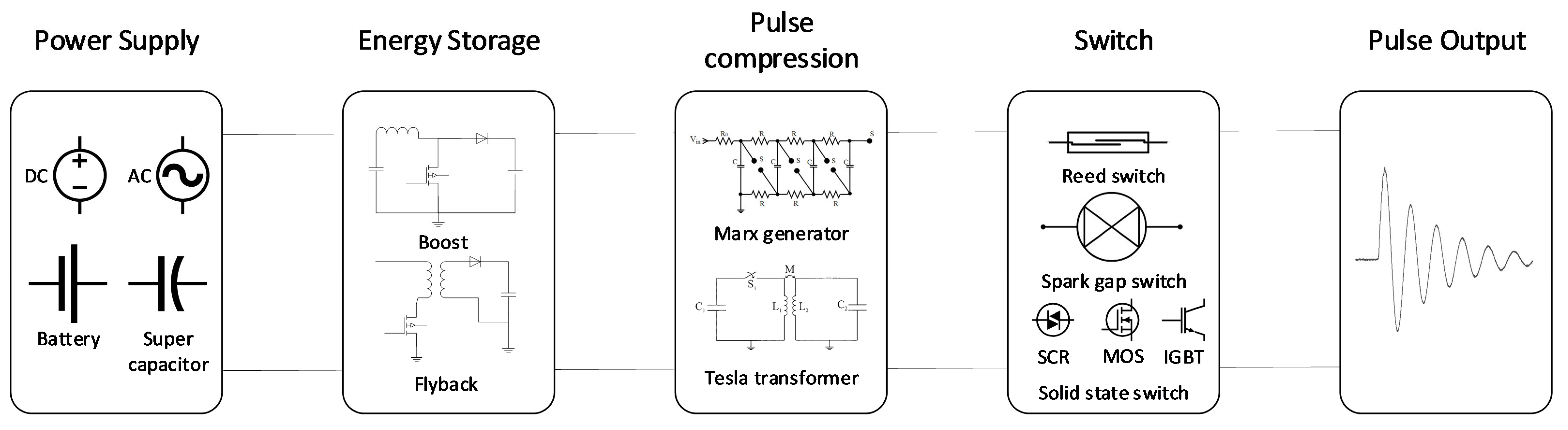
As illustrated in Figure 1, the architecture of a short pulse generator generally utilizes a cascaded topology consisting of four distinct operational stages: power supply, energy storage, pulse compression, and switching control [21,22]. The initial energy is derived from the power supply module, which can employ standard AC/DC power sources, high-capacity batteries, or supercapacitors [23,24]. Furthermore, in advanced integrated systems, the initial energy can also be acquired through emerging wireless power transfer technologies [25]. This energy is subsequently conditioned during the energy storage phase, where intermediate storage capacitors are charged to the initial voltage level via high-voltage converter topologies such as boost or flyback circuits [21]. The core high-voltage generation process takes place during the pulse compression stage. This stage employs voltage-doubling and shaping networks, such as Marx generators [26,27] or Tesla transformers [28], to achieve the necessary peak voltage and pulse steepness. The final pulse output is governed by the switching stage. The integration of electromechanical reed switches, high-voltage spark gap switches, or solid-state semiconductor devices (e.g., thyristors, MOSFETs, and IGBTs) in this stage is contingent upon the frequency and power requirements, thereby ensuring precise commutation [29,30].
A critical challenge in the development of compact and miniaturized pulse generators is the adaptation of low-voltage power inputs within a highly restricted volume while still achieving the required high-power pulse outputs. This discrepancy in power levels underscores the necessity for an efficient energy storage system that can accumulate energy from the source and release it instantaneously [31,32]. Among the various technologies available, capacitors remain the classic and quintessential choice for energy storage due to their fast discharge rates, high reliability, and scalability. However, the high-voltage transients inherent in their operation pose significant electrical safety hazards. In contrast to operational risks, which can be mitigated through external insulation or physical isolation, the dangers stemming from residual stored energy persist even after power disconnection, rendering passive barrier measures ineffective. In order to ensure the safety of personnel, contemporary designs must rigorously adhere to pertinent safety standards. For instance, IEC 62368-1 categorizes such energy storage systems as Category 3 hazards [33], stipulating that residual voltage must decay to safe levels (typically below 60 V DC) within two seconds following the disconnection of power. Meeting these stringent time constraints within the confined spaces of modern compact systems imposes extreme demands on power density [34,35].
The necessity for rapid and reliable discharge of high-voltage buses or energy storage capacitors extends far beyond compact pulse generators, playing a critical role in a wide spectrum of applications, including electric vehicles (EVs), renewable energy inverters, medical equipment, and high-power industrial drives [36,37]. To mitigate the safety hazards associated with these phenomena, various discharge mechanisms have been developed and deployed. In essence, these strategies can be classified into two primary categories: passive and active discharge mechanisms. While passive methods, such as the implementation of bleeding resistors, offer structural simplicity, they inherently exhibit continuous power loss and slow, uncontrollable discharge rates. Conversely, active mechanisms offer faster and highly controllable discharge capabilities, though often at the expense of increased system complexity and the need for auxiliary power. A thorough comparison of these conventional topologies, emphasizing their operational characteristics, power leakage, and inherent limitations, is presented in Table 1.
As demonstrated in Table 1, passive mechanisms are inherently constrained in their capabilities. They exhibit a deficiency in dynamic controllability, incapable of facilitating expeditious discharge, and exhibit adverse interference with standard system operation through continuous power dissipation. Consequently, contemporary research has undergone a shift in focus, with a notable emphasis on active discharge solutions. A synopsis of the extant literature pertaining to these active discharge mechanisms is provided in Table 2.
As demonstrated by the data presented in Table 2, the majority of existing active discharge topologies are designed with large-scale applications, such as electric vehicles (EVs) or heavy motor drives, in mind. These conventional methods generally address substantial energy storage capacitances and necessitate the use of voluminous components. Moreover, they mandate the continuous transmission of auxiliary control signals during the discharge phase. However, a significant discrepancy emerges when these solutions are applied to compact high-voltage pulse generators. These systems are distinguished by their high operational voltages and low target capacitances, which are further compounded by their limited spatial dimensions. The cumbersome physical footprint and auxiliary power dependency of current methods render them impractical for these highly integrated environments. Consequently, there is an imperative need for a novel discharge architecture that utilizes small surface-mount components and single-layer PCB to execute rapid, safe discharge autonomously, thereby eliminating the reliance on external auxiliary inputs.
In order to address these imperatives, the present paper proposes a novel self-powered, fast-response discharge topology that leverages cascaded depletion-mode NMOS transistors. The proposed circuit is designed to function reliably even in the event of a complete system power failure. This objective is accomplished by capitalizing on the inherent normally-on characteristic of depletion-mode NMOS devices, thereby eliminating the requirement for external auxiliary power supplies. The topology incorporates a cascaded configuration to withstand high-voltage transients while maintaining a compact footprint suitable for miniaturized pulse generators. Furthermore, a control mechanism has been integrated to facilitate a constant-current discharge profile. This approach effectively addresses the trade-off between the rapid discharge requirements and the stringent volume constraints of contemporary compact pulsed-power systems.
The rest of this paper is systematically organized as follows. Section 2 outlines the design and theoretical operational principles of the proposed discharge circuit topology. Section 3 details the simulation analysis conducted to evaluate parameter sensitivity and statistical reliability. Section 4 presents experimental verification through hardware prototype testing, focusing on discharge performance, long-term repeatability, and thermal stability. Finally, the discussion and concluding remarks are presented in Section 5 and Section 6, respectively.

2. Circuit Topology Design

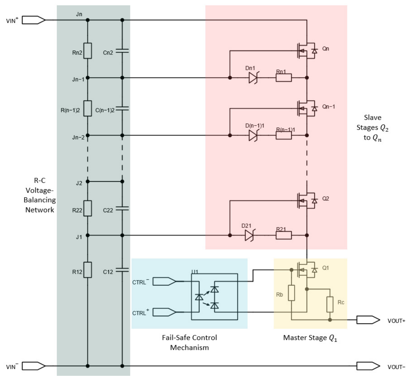
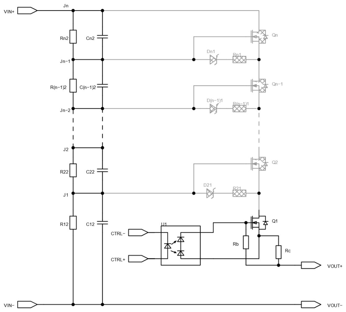
As illustrated in Figure 2, the proposed topology utilizes a cascaded configuration of depletion-mode NMOS transistors to achieve high-voltage handling capabilities. The circuit under consideration is principally constituted by a voltage-balancing network, a cascaded MOSFET switch array, and an isolated gate drive circuit.
The input source is applied across terminals V I N + and V I N . A passive static voltage-balancing network, consisting of N series-connected resistors R 12 to R n 2 and parallel capacitors C 12 to C n 2 , is placed in parallel with the main power stage. This network functions by dividing the high input voltage into equal steps at nodes J 1 through J n . This ensures uniform voltage distribution across the switch stack in the off-state.
The primary current path is established through an N -stage series string of MOSFETs, denoted as Q 1 through Q n . The current flows sequentially from the drain of the top-side transistor Q n , cascading down through intermediate stages, and finally through the bottom-side transistor Q 1 . The control mechanism is divided into two distinct parts:
  • The Master Stage Q 1 : The bottom-most transistor Q 1 fuctions as the master control switch. The gate is driven by an optocoupler U 1 , which provides the necessary galvanic isolation for the control signals C T R L + and C T R L . A pull-down resistor R b is connected between the gate and source of Q 1 to ensure a reliable off-state in the absence of a control signal. The source of Q 1 is connected to the output terminal V O U T + via a current-limiting resistor R c .
  • The Slave Stages Q 2 to Q n : The upper transistors fuction in a self-biased cascade follower configuration. The gate of each upper-stage MOSFET Q k (where k   >   1 ) is referenced to the voltage divider node J k 1 of the previous stage. For instance, the gate of Q 2 is connected to node J 1 , and the gate of Q n is connected to node J n 1 .
In order to safeguard the gate dielectrics of the upper-stage MOSFETs, a clamping network comprising a Zener diode (e.g., D 21 to D n 1 ) and a series resistor (e.g., R 21 to R n 1 ) is connected between the gate and source of each respective transistor. These Zener diodes D k 1 serve to clamp the gate-source voltage V G S within safe operating limits during switching transients. The reverse breakdown voltage of the Zener diodes is selected to be significantly lower than the static voltage drop across the corresponding balancing resistors R k 1 . This ensures that the Zener diodes effectively protect the MOSFETs without interfering with the static voltage distribution determined by the resistive network.

2.1. Depletion-Mode NMOS Characteristics and Self-Biasing Principle

The selection of depletion-mode NMOS transistors as the core switching elements is fundamentally motivated by their inherent normally-on characteristic. In contrast to enhancement-mode devices, which require an external gate bias to establish a conductive channel, a depletion-mode NMOS maintains the on-state at zero or part negative gate-source bias. This property renders it an optimal selection for fail-safe discharge mechanisms, wherein switches are required to default to the conducting state automatically upon loss of the control signal.
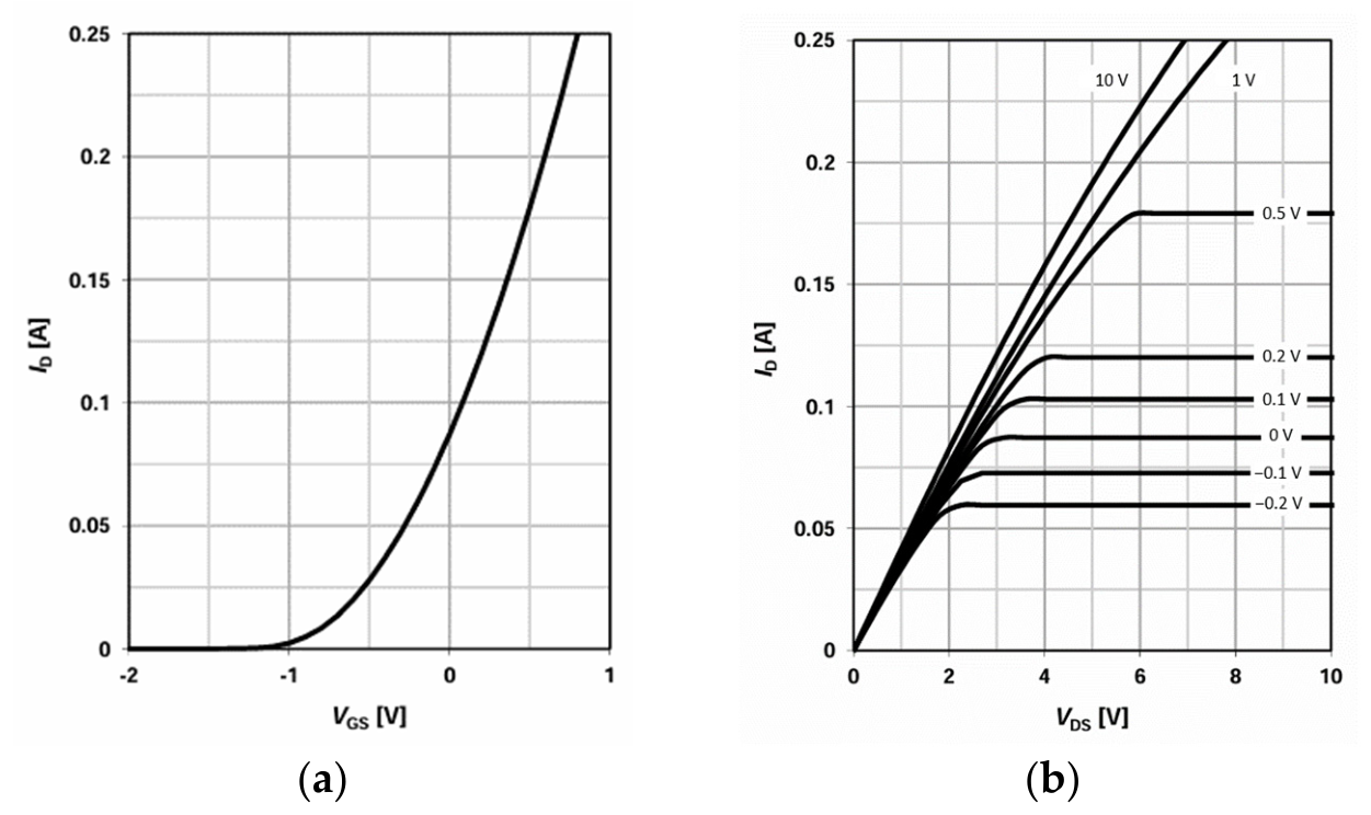
The electrical behavior of the depletion-mode N-channel MOSFET is characterized by its transfer and output characteristics, as illustrated in Figure 3. The transfer characteristic, denoted by I D versus V G S , demonstrates a decline in the drain current I D as the gate-source voltage V G S becomes more negative, ultimately reaching a state of zero when the gate-source voltage V G S attains the pinch-off voltage V G S o f f . The output characteristic, denoted by I D versus V D S , demonstrates that for a constant V G S , I D remains relatively constant once the drain-source voltage V D S exceeds the saturation voltage. This behavior is characterized by a distinct constant-current response [42].
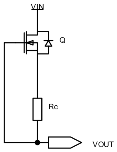
Utilizing this saturation behavior, a straightforward yet remarkably efficacious constant current source can be engineered, as demonstrated in Figure 4. This configuration employs a self-biasing mechanism, wherein a source resistor, designated as R C , is connected in series with the source terminal. The gate is referenced to the bottom of R C [43].
In this configuration, the voltage drop across R C provides a negative bias to the gate relative to the source, expressed as:
V G S = I D × R C
Assuming the depletion-mode MOSFET operates in the saturation region, the drain current is governed by the square-law equation:
I D = I D S S 1 V G S V G S o f f 2
The substitution of Equation (1) into Equation (2) results in the derivation of the relationship between the target constant current I s e t and the required resistance R C . In the event that a desired current I s e t is established, with the stipulation that I s e t is less than the designated threshold, referred to as I D S S , the requisite resistance value can be determined through:
R C = V G S o f f I s e t 1 I s e t I D S S
This negative feedback mechanism ensures that any increase in I D leads to a more negative V G S ; consequently, the current rise is counteracted, thereby stabilizing the output current against variations in the supply voltage, provided the device remains in saturation.
This self-biasing principle constitutes the core mechanism of the proposed topology. The master switch Q 1 , in conjunction with the current-limiting resistor R C , constitutes a self-biased constant-current sink. In the discharge mode, the normally-on characteristic of Q 1 ensures automatic activation without the need for an external drive. The source degeneration provided by R C stabilizes the discharge current against bus voltage decay.
The intrinsic characteristics of depletion-mode MOSFETs render them highly suitable for fail-safe discharge applications. However, the direct employment of a single device to discharge high-voltage energy storage components imposes extreme demands on its breakdown voltage B V D S S . Monolithic ultra-high-voltage depletion-mode devices necessitate cumbersome physical packaging to guarantee sufficient creepage distances, a practice that profoundly contravenes the imperative for miniaturization. Additionally, a significant discrepancy in parameters has been identified. These specialized devices are typically designed to manage substantial on-state currents. However, safety discharge circuits typically operate within the milliampere to low-ampere range. This discrepancy can lead to increased costs and wasted current-handling capacity. Consequently, the distribution of high-voltage stress across multiple smaller, commercially available low-voltage devices through the cascaded configuration previously described is imperative for achieving a compact, cost-effective design.

2.2. Operational Principle and Theoretical Analysis of Mode Control

The proposed topology is controlled via the differential terminals C T R L + and C T R L , which drive the isolation optocoupler U 1 . To ensure system safety, the control logic is designed with a normally-on characteristic that utilizes the inherent properties of depletion-mode MOSFETs. The operation consists of two primary states, which are determined by the input voltage level:
  • Discharge Mode ( V C T R L = 0 /Logic Low)
The discharge mode signifies the fail-safe state of the proposed topology, which is automatically engaged in the event of a power failure, emergency shutdown, or loss of the control signal (i.e., V C T R L = 0 ). As illustrated in Figure 5, the sequence of operations is initiated by the deactivation of the optocoupler U 1 .
In the absence of a drive current on the input side of U 1 , its output phototransistor enters a cutoff state, resulting in a high-impedance output. Consequently, the gate of the master switch Q 1 is pulled to its source potential via the resistor R b , establishing a gate-source voltage of approximately zero ( V G S 0 ). Due to the depletion-mode characteristic of the NMOS devices, Q 1 is normally on at zero bias. Therefore, Q 1 instantaneously enters the conduction region, thereby establishing a current path from its drain to the ground (or negative rail) through the current-limiting resistor R c .
The activation of Q 1 instigates a cascaded turn-on process for the upper stages Q 2 to Q n through a domino effect:
  • As Q 1 conducts, it pulls down the source potential of the subsequent stage, Q 2 ;
  • The gate of Q 2 , however, remains referenced to the voltage divider node J 1 . This node is maintained by the parallel capacitor C 12 and resistor R 12 ;
  • This potential difference generates a positive effective gate-source voltage for Q 2 , driving it into conduction;
  • This mechanism propagates sequentially up the stack until the topmost transistor Q n is activated.
Subsequent to the attainment of complete conductivity throughout the string, the energy stored in the high-voltage capacitors or the input source V I N is discharged through the MOSFET chain. This configuration leverages the inherent saturation characteristics of depletion-mode MOSFETs. In the event that V G S is maintained at a value approximating zero or negative voltage, Q 1 functions within its saturation region, thereby operating as a constant current sink. This operation is subject to limitations imposed by two factors: the saturation drain current I D S S and the source degeneration effect of R c .
During this process, the Zener diode networks D 21 to D n 1 positioned between the gate and source of each upper-stage MOSFET serve a dual purpose: they clamp the V G S to prevent gate oxide breakdown during the transient voltage redistribution and ensure that the transistors operate within their safe operating area (SOA) during the high-voltage discharge.
As the discharge current I d i s flows through R c , it elevates the source potential V S of Q 1 . Given the grounded nature of the gate, the effective gate-source voltage, denoted by V G S , assumes a negative value:
V G S = V G V S = 0 I d i s R c = I d i s R c
For a depletion-mode MOSFET operating in the saturation region ( V D S > V G S V G S o f f ), the drain current is governed by the Shockley equation:
I D = I D S S 1 V G S V G S o f f 2
where I D S S is the saturation drain current at zero bias, and V G S o f f is the pinch-off voltage (a negative value for depletion-mode NMOS) [44]. Substituting Equation (4) into Equation (5) yields the governing equation for the discharge current:
I d i s = I D S S 1 I d i s R c V G S o f f 2 = I D S S 1 + I d i s R c V G S o f f 2
This relationship indicates that I d i s is self-stabilized to a value less than I D S S . The resistor R c functions as a programming element. By selecting an appropriate resistance value, the discharge current can be precisely defined.
The total high voltage V I N t is distributed across the cascaded stages. Assuming a balanced resistive network R 12 = = R n 2 , the potential at the k -th node J k is linear:
V J k = V I N t k n
Therefore, the drain-source voltage for each stage is clamped to V D S V I N t / n , ensuring uniform stress distribution.
The discharge time T d i s is defined as the duration required to deplete the energy storage capacitance C s t o r e from a initial high voltage V i n i t to a safe threshold V s a f e . This discharge time derived from the constant-current discharge integration:
T d i s = V s a f e V i n i t C s t o r e I d i s d V = C s t o r e V i n i t V s a f e I d i s
This linear decay characteristic is in contrast to the exponential decay of passive RC bleeders. The proposed circuit utilizes the self-biased topology Q 1 and R c to maintain a high and constant discharge rate even as the bus voltage drops. This approach significantly reduces the time-to-safe interval compared to traditional methods.
A critical reliability metric for fail-safe systems is the deterministic consistency of the discharge time T d i s across varying manufacturing tolerances and environmental conditions. Commercial depletion-mode MOSFETs inherently exhibit significant discrete dispersion in both their zero-bias saturation current I D S S and pinch-off voltage V G S o f f . Additionally, the thermoelectric properties of I D S S are found to be significantly temperature-dependent, owing to the diminished carrier mobility that occurs at elevated junction temperatures. A formal sensitivity analysis is imperative to quantitatively evaluate the robustness of the proposed constant-current regulation against such device dispersion.
By implicitly differentiating Equation (6) with respect to V G S o f f , the absolute sensitivity of the discharge current to the pinch-off voltage is derived as:
I d i s V G S o f f = 2 I d i s R c I D S S I d i s V G S o f f V G S o f f 2 R c I D S S I d i s
Similarly, differentiating Equation (6) with respect to the saturation current I D S S yields:
I d i s I D S S = I d i s V G S o f f I D S S V G S o f f 2 R c I D S S I d i s
In order to comprehend the impact of these current variations on the system-level safety threshold, the chain rule is employed to analyze Equation (8). The paramount engineering concern pertains to the relative sensitivity coefficient S x T d i s , which quantifies the percentage change in the total discharge time T d i s , resulting from a change in the intrinsic parameter x . The relative sensitivity coefficients for V G S o f f and I D S S are respectively expressed as:
S V G S o f f T d i s = T d i s V G S o f f V G S o f f T d i s = 2 R c I D S S I d i s V G S o f f 2 R c I D S S I d i s
S I D S S T d i s = T d i s I D S S I D S S T d i s = V G S o f f V G S o f f 2 R c I D S S I d i s
In the context of depletion-mode NMOS devices, the pinch-off voltage is defined as negative, indicating that the threshold voltage V G S o f f is less than zero. Consequently, the denominator in both relative sensitivity equations is the sum of two negative terms. An analysis of these bounds reveals a mathematically characteristic of the proposed topology. Specifically, the magnitudes of both relative sensitivity coefficients are constrained to be less than unity.
S V G S o f f T d i s < 1 and S I D S S T d i s < 1
This mathematical boundary demonstrates that the self-biasing source degeneration resistor R c effectively functions as an attenuation factor. Consequently, even if standard commercial MOSFETs demonstrate considerable batch-to-batch variation in V G S o f f or I D S S , the resulting fractional variance in the safety discharge time T d i s will invariably be disproportionately smaller.
Moreover, this attenuation inherently safeguards the system against thermal drift. During the high-voltage transient, the MOSFETs dissipate energy, causing an increase in junction temperature and, consequently, a decrease in I D S S . According to the sensitivity function, the thermal reduction causes a slight, attenuated elongation of T d i s . This dynamic reduction in peak power dissipation prevents thermal runaway, thereby ensuring the system’s reliable compliance with safety standards under extreme, non-ideal conditions.
Operating in the linear saturation region inherently subjects the discharge circuit to simultaneous high-voltage stress. In order to comprehensively assess the thermal reliability and ensure that the devices operate strictly within their Safe Operating Area, it is essential to evaluate the instantaneous power dissipation.
During the constant-current discharge phase, the bus voltage v t decays linearly from the initial voltage V i n i t . The total instantaneous power dissipated by the entire topology at any given time is expressed as:
P d i s t = v t I d i s = V i n i t I d i s C s t o r e t I d i s
The total thermal energy is distributed by the passive current-limiting resistor R c and the active cascaded MOSFET string. Given the strict regulation of the discharge current, the instantaneous power dissipated by the source resistor remains constant throughout the active window.
P R c = I d i s 2 R c
Therefore, under the assumption that the static and dynamic voltage-balancing network effectively equalizes the voltage stress across the N cascaded stages, the instantaneous power dissipation imposed on each individual depletion-mode MOSFET P Q t is calculated by subtracting the resistor’s fixed dissipation from the total power and dividing by the number of stages.
P Q t = v t I d i s I d i s 2 R c N = V i n i t I d i s C s t o r e t I d i s I d i s 2 R c N
This mathematical formulation underscores a pivotal thermal benefit inherent to the proposed topology. The peak power dissipation per MOSFET occurs precisely at the initiation of the discharge ( t   =   0 ), when the bus voltage is at its absolute maximum. The peak thermal stress per stage is defined as:
P Q _ p e a k = V i n i t I d i s I d i s 2 R c N
It has been demonstrated that by deliberately shifting a portion of the initial thermal burden onto the passive power resistor, denoted by the subtractive term I d i s 2 R c , the peak instantaneous power dissipation upon the semiconductor junctions is inherently reduced. This distributed thermal mechanism is designed to ensure that the transient thermal impedance of the MOSFETs is not exceeded. As a result, the cascaded string can safely navigate the high-stress linear region without violating the boundary conditions of the devices’ SOA limits.
In order to undertake a fundamental evaluation of the thermal stability of the proposed safety discharge topology, it is necessary to conduct a quantitative analysis of the temperature-dependent characteristics of the depletion-mode MOSFET. The thermal drift of the steady-state discharge current I d i s is governed by the competing physical mechanisms of carrier mobility, denoted by μ T , and the pinch-off voltage V G S o f f T .
The carrier mobility demonstrates a negative temperature coefficient due to enhanced acoustic phonon scattering at elevated temperatures, which can be mathematically modeled as:
μ T = μ T 0 T T 0 α
where T 0 is the reference room temperature and α is a material-specific mobility degradation constant. In contrast, the pinch-off voltage exhibits a positive temperature coefficient, which is attributable to the intrinsic carrier concentration shift. This can be approximated by:
V G S o f f T = V G S o f f T 0 + κ T T 0
where κ represents the temperature coefficient of the threshold voltage. It is a well-established convention in this field that this coefficient is typically positive, which indicates that the negative V G S o f f moves closer to zero.
By integrating these thermal dependencies into the classical square-law saturation model for the self-biased configuration (where V G S = I d i s R c ), the temperature-dependent discharge current is expressed as:
I d i s T = 1 2 μ T C o x W L I d i s T R c V G S o f f T 2
The differentiation of this implicit equation with respect to temperature T unveils the system’s dynamic thermal equilibrium. In the proposed topology, the self-biasing resistor R c enforces operation at a relatively high current density. In this strong-inversion saturation regime, the mobility degradation term μ /   T strictly dominates the threshold voltage shift V G S o f f / T . Consequently, the derivative I d i s / T < 0 , ensuring that the overall discharge current intrinsically exhibits a negative temperature coefficient behavior. Instantaneous power dissipation has been shown to elevate the junction temperature during a high-voltage discharge event. This, in turn, has been demonstrated to result in a deterministic, self-limiting reduction in the current I d i s . This quantitative framework demonstrates that the cascaded architecture inherently suppresses thermal runaway, thereby ensuring operations remain strictly within the dynamic SOA without the intervention of external active cooling mechanisms.
  • Blocking Mode ( V C T R L = 3.3 V / Logic   High )
The system transitions to Blocking Mode when the external control signal transitions to a logic high state (e.g., 3.3 V). This effectively isolates the input source from the load. As depicted in Figure 6, this transition is initiated by the activation of the optocoupler U 1 .
Upon reception of the high-level control signal, the internal LED of U 1 is energized. The output stage of U 1 , configured to drive the depletion-mode device, generates a specific bias voltage V b i a s across the gate-source terminals of the master switch Q 1 . In contrast to conventional enhancement-mode drivers, the polarity of this bias is configured to reduce the gate potential below the source potential.
Quantitatively, the gate-source voltage V G S 1 of Q 1 is constrained to:
V G S 1 = V b i a s
In order to ensure the reliable cutoff of the depletion-mode MOSFET, it is necessary that the magnitude of this generated bias exceed the absolute value of the device’s threshold voltage V G S o f f , which is negative for depletion NMOS. The cutoff condition is satisfied when:
V G S 1 < V G S o f f < 0 V b i a s > V G S o f f
In this condition, the conductive channel of Q 1 is fully depleted, forcing the transistor into the cutoff region ( I D 0 ).
The deactivation of the bottom-stage MOSFET Q 1 instigates a synchronous turn-off sequence for the upper stages Q 2 to Q n through a self-biasing mechanism.
  • Once Q 1 turns off, the current path to the ground undergoes an interruption.
  • Consequently, the source potential V S 2 of the second-stage MOSFET Q 2 (which is connected to the drain of Q 1 ) begins to rise due to the leakage current from the high-voltage side.
  • The gate of Q 2 is clamped to a fixed potential V J 1 by the resistive divider network R 12 .
  • Conversely, an increase in V S 2 results in a decrease in the gate-source voltage of Q 2 . This relationship can be expressed as V G S 2 = V J 1 V S 2 . It is evident that when the value of V S 2 increases to a sufficient extent, resulting in a decrease in V G S 2 to below the threshold value, Q 2 will transition into the cutoff region.
This mechanism propagates upward through the stack. In the steady Blocking Mode, the drain-source voltage V D S of each MOSFET is effectively determined by the static voltage-balancing network:
V D S _ k V J k V J k 1 = V I N N
where V I N is the total DC link voltage and N is the number of stages.
In this mode, the main power loop exhibits high impedance. The sole power consumption is attributable to the static leakage current that permeates the voltage-balancing resistors R k 2 and the control side of U 1 . This configuration guarantees that the high-voltage switch can withstand the full bus voltage indefinitely while concurrently maintaining a safe, low-power standby state.
In order to comprehensively address the system’s energy profile and ensure a thorough evaluation of total losses, it is imperative to assess the static power dissipation when the circuit is operating in the standby blocking mode. In this state, the cascaded MOSFETs are driven into the cutoff region, thereby presenting a high impedance to the DC link. However, a persistent leakage path has been identified, primarily through the static voltage-balancing network.
The total standby leakage current I l e a k drawn from the high-voltage bus V i n i t is the sum of two components: the current flowing through the resistive divider string I s t r i n g and the equivalent off-state leakage current of the MOSFET stack I D S S _ l e a k . Because the design dictates that I s t r i n g 10 I D S S _ l e a k to guarantee uniform static voltage division and mitigate device dispersion, the total leakage current can be conservatively approximated by the resistive network alone:
I l e a k I s t r i n g = V i n i t k = 1 N R k 2 = V i n i t N R k 2
Consequently, the steady-state static power loss   P l e a k , which dissipates continuously by the topology during the high-voltage blocking phase, is calculated as follows:

P l e a k = V i n i t I l e a k V i n i t 2 N R k 2

2.3. Design Considerations

The reliability and performance of the proposed high-voltage discharge topology are contingent upon the precise selection of core components. The design rationale for the depletion-mode MOSFETs, voltage-balancing network, isolation interface, and current-limiting elements is detailed below.

2.3.1. Depletion-Mode MOSFETs

The selection of the power transistors is governed by three primary constraints: breakdown voltage B V D S S , saturation drain current I D S S , and the safe operating area.
  • Voltage Rating: Reliability is contingent upon the breakdown voltage of each stage exceeding the theoretical distributed voltage V I N / n by a safety margin of at least 20%. Consequently, the device is selected in such a manner that B V D S S > 1.2 V I N m a x / n . The utilization of identical devices for both the master stage, designated as Q 1 , and the slave stages, ranging from Q 2 to Q n , is implemented to ensure uniform thermal and electrical characteristics.
  • Linear Mode Capability: It is imperative that the MOSFETs possess a robust DC SOA, given that the circuit operates in the saturation region during the discharge phase and functions as a constant current source. Devices that have been optimized for linear applications or those with a low thermal resistance junction-to-case R θ J C are preferred to prevent thermal runaway caused by simultaneous high voltage and current stress.
  • Threshold Voltage: The pinch-off voltage must be sufficiently negative (typically ranging from −1.0 to −3.5 volts) to provide a clear distinction between the conducting state and the blocking state. This must be achieved while remaining within the drive capability of the optocoupler circuit.

2.3.2. Voltage-Balancing Network

The passive balancing network plays a critical role in mitigating the effects of parameter mismatch among the cascaded devices [45].
  • Static Balancing Resistors R k 2
These resistors ensure uniform voltage division in the steady-state Blocking Mode. The resistance value is determined by a trade-off between leakage loss and balancing efficacy. It is imperative that the current flowing through the resistor string, denoted here as I s t r i n g , is at least 5 to 10 times larger than the maximum drain-source leakage current I D S S _ l e a k of the MOSFETs at elevated temperatures.
R k 2 V I N / n 10 I D S S l e a k
  • Dynamic Balancing Capacitors C k 2
During the transient switching phases (i.e., discharge to blocking or vice versa), parasitic capacitances C o s s can induce substantial voltage imbalances. The parallel capacitors, denoted by C k 2 , are selected to dominate these parasitics. A prevailing principle in the field suggests that the balancing capacitance should be considerably larger than the device’s output capacitance.
C k 2 > 10 C o s s m a x
This ensures that the voltage distribution during transients is governed by the external capacitors rather than the nonlinear intrinsic capacitances of the MOSFETs.

2.3.3. Control Interface and Isolation

The control stage bridges the low-voltage logic and the high-voltage power loop.
  • Photovoltaic-Output Optocoupler U 1
Conventional gate drive optocouplers necessitate an external secondary power rail; however, U 1 is selected as a photovoltaic-output optocoupler. The device’s internal configuration consists of a highly efficient Gallium Aluminum Arsenide (GaAlAs) infrared LED optically coupled to a series-connected photodiode array [46]. Upon activation, the photodiode array functions as an isolated voltage source, generating an open-circuit voltage V O C that exceeds 7 V. This voltage magnitude provides a robust safety margin for driving the gate-source voltage V G S of the depletion-mode MOSFET well below its negative cutoff threshold V G S o f f , which is typically −1.5 V to −3.5 V. This ensures a reliable blocking mode. The device also offers superior galvanic isolation, effectively decoupling the control logic from high-voltage transients.
  • Gate-Source Impedance Matching Resistor R b
The selection of R b is strictly constrained by the output characteristics of the photovoltaic coupler. Given the inherent limitations of the photodiode array’s drive capability, typically ranging from microamps, it is essential to ensure sufficient load impedance to prevent voltage collapse. A resistor in the mega-ohm class is selected for R b (e.g., 1 or 5 MΩ). This high resistance reduces the leakage current drawn from U 1 , enabling the gate voltage to reach the required cutoff level (>7 V) during the Blocking Mode. Conversely, when the control signal is removed, the photovoltaic output ceases. In this configuration, R b serves as the discharge path for the gate-source capacitance C g s . This ensures that the gate-source voltage V G S relaxes to zero potential, thereby enabling the passive activation of the depletion-mode MOSFET Q 1 .

2.3.4. Current-Limiting Resistor

The resistor R c fulfills two distinct functions: current programming and thermal management. As elucidated in Section 3.1, R c establishes the negative feedback that stabilizes the discharge current I d i s . The value of the discharge is determined by the target discharge time T d i s and the desired current   I d i s as illustrated in Equation (8). During the discharge event, the resistor dissipates a portion of the stored energy. It is imperative that the power resistor possesses a high pulse-load capability. Non-inductive wirewound or thick-film power resistors are preferred to minimize parasitic inductance, which could induce oscillation during the fast turn-on transient.

3. Simulation Analysis

3.1. Simulation Setup and Nominal Performance

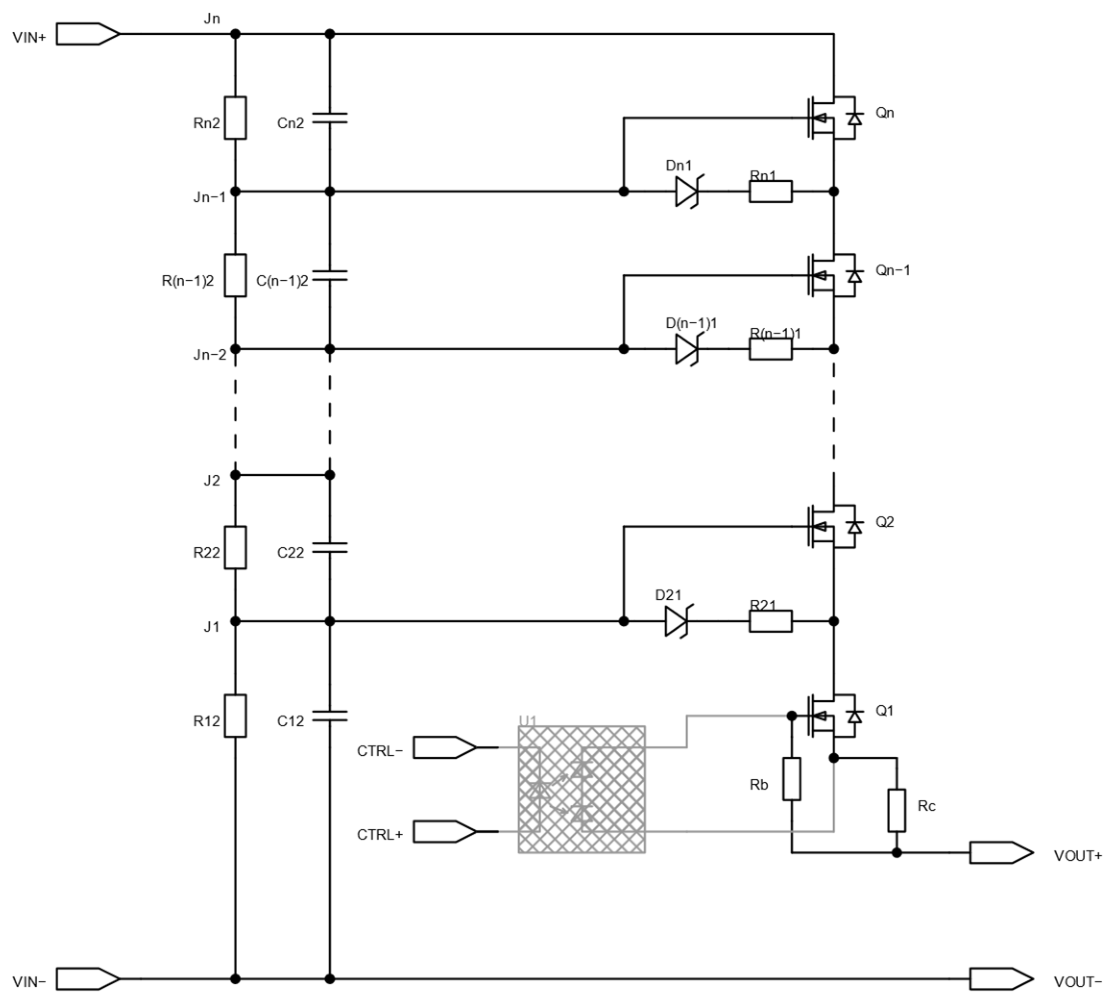
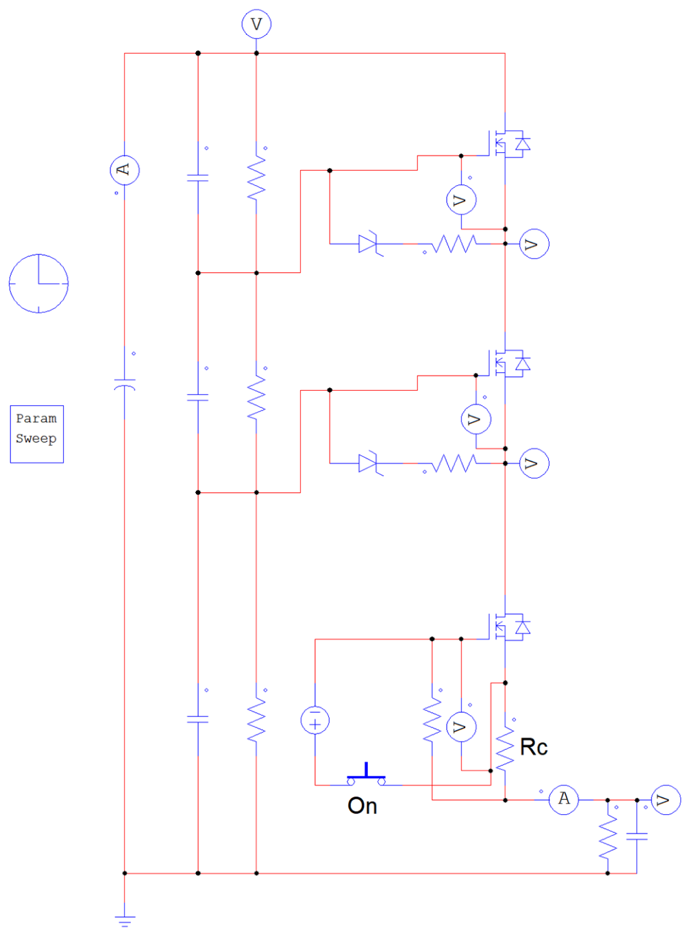
A detailed simulation study was conducted to validate the theoretical analysis presented in Section 2 and to comprehensively evaluate the dynamic performance of the proposed circuit. The implementation of the simulation model was executed within the PSIM 2025.0 software environment. The comprehensive simulation schematic of the proposed high-voltage safety discharge topology is illustrated in Figure 7.
The configuration of the simulation setup is designed to replicate critical operating conditions, including the static high-voltage blocking state and the transient constant-current discharge phase. To ensure the fidelity of the results, the Infineon BSP135 was selected as the specific depletion-mode MOSFET model. The selection of this device was predicated on its high breakdown voltage B V D S S and its compact SOT-223 package, in conjunction with its demonstrated reliability in established high-voltage applications. Consequently, the simulation parameters are closely aligned with the characteristics of practical hardware implementation. The key system specifications and component parameters employed in the simulation are enumerated in Table 3.
In addition, to accurately simulate the transient and static behaviors of the selected depletion-mode MOSFET, the device model was meticulously configured based on its datasheet characteristics. The configuration parameters for the BSP135 model employed in the simulation are enumerated in Table 4.
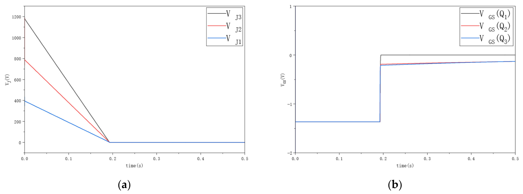
The dynamic response of the proposed topology during the safety discharge phase is evaluated by initiating a control signal transition ( V C T R L set to logic low). The ensuing discussion will focus on the simulation results corresponding to an initial bus voltage of 1200 V and a load capacitance of 220 nF. These results are presented in Figure 8.
As illustrated in Figure 8a, the transient voltage waveforms at the inter-stage nodes V J 1 to V J 3 are presented. The node voltages undergo a synchronous decrease, thereby ensuring the maintenance of equal spacing throughout the discharge process. This finding serves to substantiate the efficacy of the balancing network in mitigating overvoltage stress on a per-MOSFET stage basis. The discharge curves manifest a unidirectional linear slope, contrasting with the exponential decay characteristic of passive resistor bleeders. This linearity indicates that the discharge current remains constant, effectively independent of the decreasing bus voltage.
As illustrated in Figure 8b, the gate-source voltage V G S dynamics of the cascaded MOSFETs Q 1 to Q 3 are revealed, unveiling the mechanism of the self-biased constant current operation. During the 0 to 0.2 s time interval, the circuit operates in constant-current mode, with each transistor’s gate-source voltage V G S maintaining a stable negative plateau. This negative bias is generated by the voltage drop across the source resistor R c , which clamps the device in saturation to regulate the discharge current. The discharge process is complete after 0.2 s. When the stored energy is depleted, the discharge current ceases, and the negative feedback voltage across R c disappears. Consequently, the voltage across the primary switch Q 1 reverts to zero. A negligible amount of residual negative bias persists across some MOSFETs due to charge retention effects in the output capacitance. However, this potential remains significantly above the cutoff threshold V G S o f f , thereby ensuring the device remains in the on state for subsequent cycles.
The system successfully discharges the 220 nF capacitor bank from 1200 V to a safe voltage level (near 0 V) in approximately 0.2 s when the current-limiting resistor R c is set to 1 kΩ. This outcome underscores the circuit’s capacity to facilitate expeditious and foreseeable safety discharging.

3.2. Programmability and Mode Transition

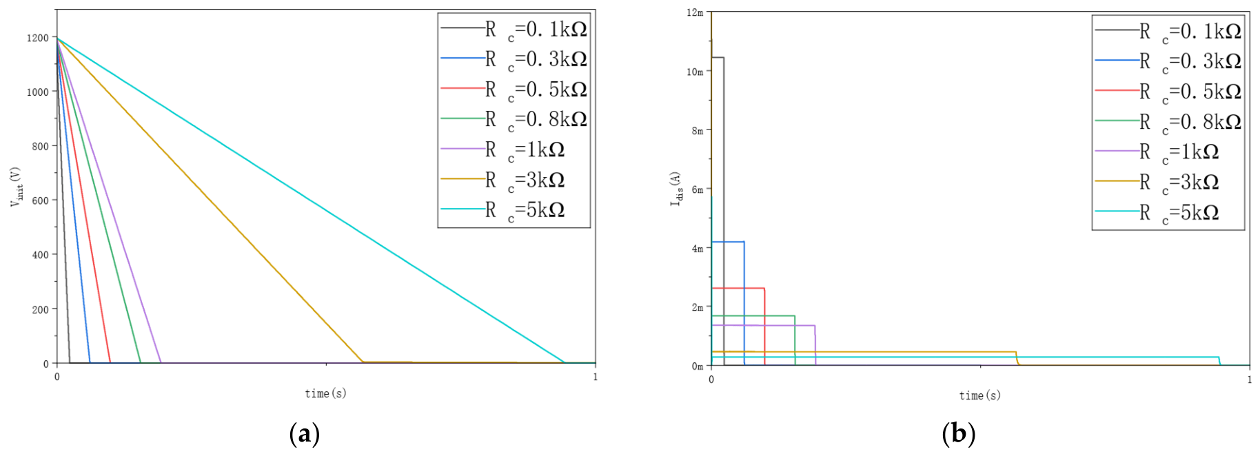
A parametric sweep analysis was conducted on the current-limiting resistor R c to verify the programmability of the discharge current and its impact on the safety discharge time. The resistance value was systematically increased from 0.1 kΩ to 5 kΩ. The simulation results are outlined in Figure 9.
As illustrated in Figure 9a, the bus voltage decay profiles vary with different R c values. It was observed that the discharge curves maintain a strict linear decay characteristic across the entire range of resistances. This finding indicates that the topology maintains robust constant-current operation, irrespective of the specific current setpoint. The discharge duration demonstrates a direct correlation with the resistance value. As the resistance R c increases, the slope of the discharge curve becomes shallower, leading to a prolonged discharge time. This finding indicates that the safety time window can be meticulously customized by selecting the appropriate R c value to align with specific system requirements.
As illustrated in Figure 9b, the corresponding discharge current I d i s waveforms are depicted. The simulation results unequivocally demonstrate that the magnitude of the constant discharge current is inversely modulated by R c . The waveforms manifest as stable, unvarying plateaus, suggesting that the negative feedback mechanism (source degeneration) effectively compensates for the fluctuating drain-source voltage during the discharge process. The relationship between the steady-state current amplitude and R c aligns with the theoretical model derived in Equation (8). For instance, an increase in R c from 0.1 kΩ to 5 kΩ results in a proportional reduction in the discharge current, thereby validating R c as an effective programming element for the discharge rate.
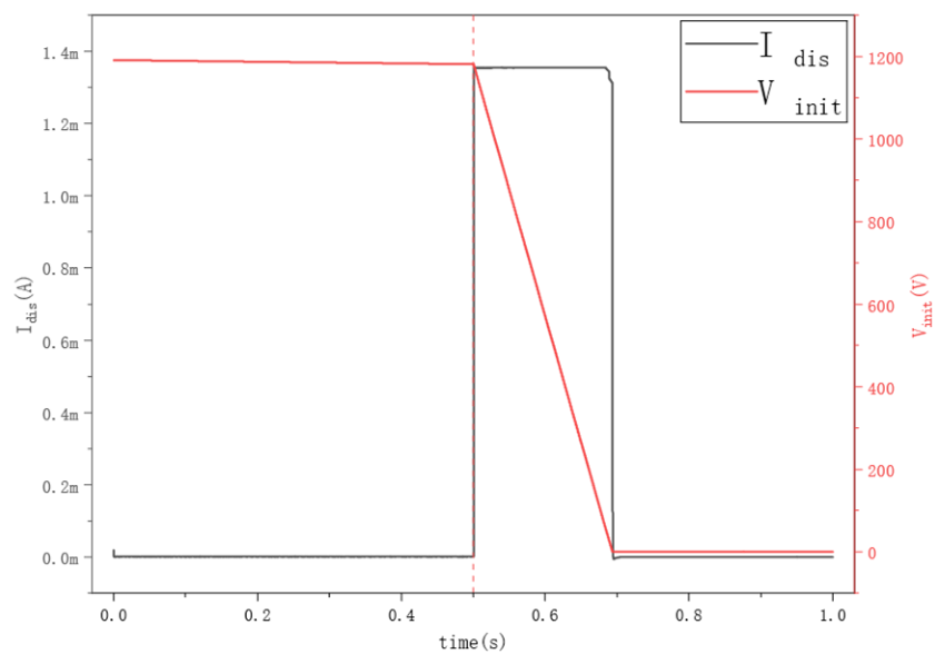
In order to validate the mode transition capability and the system’s rapid response to an emergency shutdown command, a transient simulation of the switching sequence was performed. The control signal V C T R L transitioned from a Logic High state, also referred to as Blocking Mode, to a Logic Low state, otherwise termed Discharge Mode, at a precise time instant t   =   0.5   s . The resulting dynamic waveforms of the bus voltage V i n i t and the discharge current I d i s are plotted in Figure 10.
Prior to the specified time frame, the circuit functions in a state of Blocking Mode, during which the discharge current is effectively negligible, and the high voltage remains constant. At the moment of signal removal, the system exhibits an immediate response. The discharge current I d i s exhibits a pronounced increase, reaching its steady-state value with minimal delay. This rapid activation process serves to confirm the fast intrinsic switching speed of the depletion-mode MOSFETs. Subsequent to the activation, the bus voltage undergoes a linear decay, decreasing from an initial 1200 V to a safe voltage level (near 0 V) over a duration of approximately 0.2 s. Throughout the specified discharge window, the value of I d i s ranges from 0.5 to 0.7 s, exhibiting consistent stability, with no discernible oscillatory tendencies or overshoot.
The simulation results unequivocally demonstrate the circuit’s ability to seamlessly transition from the standby blocking state to the active safety discharge state. The absence of current spikes during the transition, in conjunction with the linearity of the voltage drop, serves to further validate the design of the self-biased control loop.

3.3. Sensitivity Analysis of Intrinsic Parameters

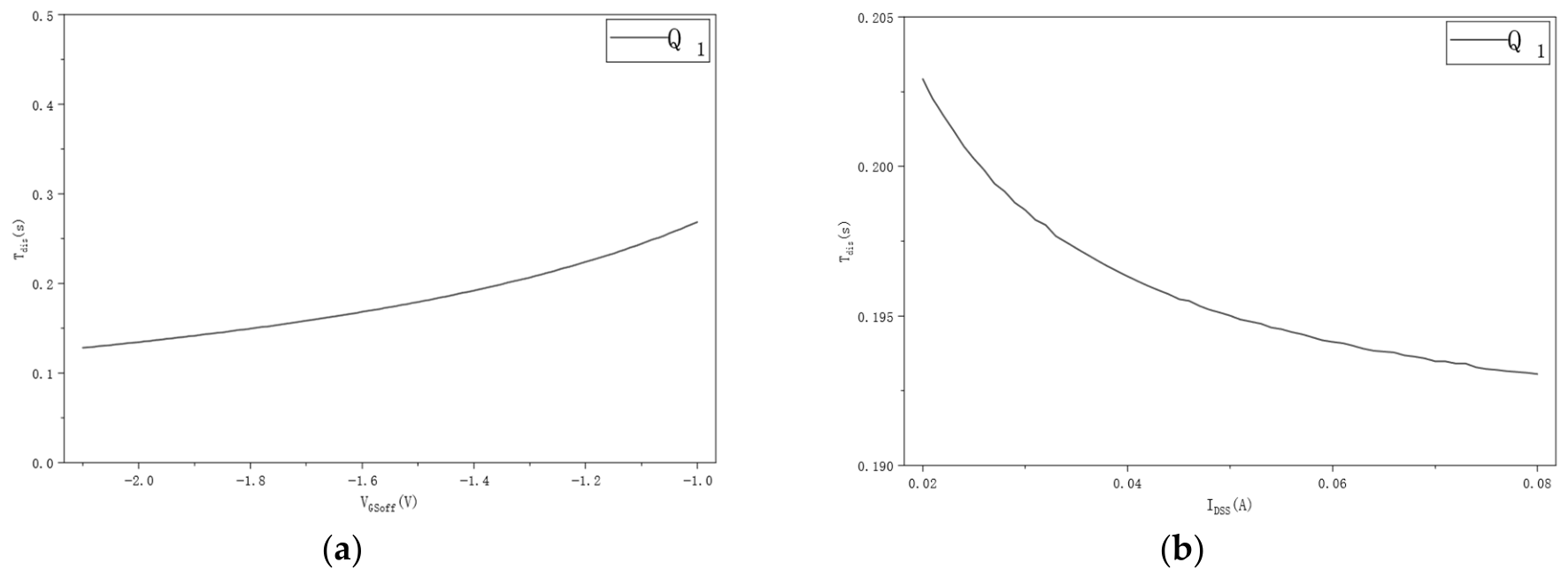
In order to validate the theoretical sensitivity model derived in Section 2.2 and assess the system’s robustness against semiconductor manufacturing tolerances, a parametric sweep analysis was conducted. The master depletion-mode MOSFET Q 1 was subjected to variations in its core intrinsic parameters, namely the pinch-off voltage V G S o f f and the zero-bias saturation current I D S S . The current-limiting resistor was maintained at 1 kΩ and the bus voltage at 1200 V. The corresponding variations in the total discharge time T d i s are illustrated in Figure 11.
As illustrated in Figure 11a, V G S o f f was swept from 2.1   V   to   1.0   V to simulate extreme gate threshold dispersion. While the absolute discharge time T d i s displays a nonlinear increase as V G S o f f becomes less negative, the proportional variation strictly adheres to the mathematical boundaries established by the theoretical model. It has been demonstrated that the self-biasing feedback acts as an attenuation factor, thereby constraining the fractional change in T d i s . This finding provides empirical validation that the magnitude of the relative sensitivity coefficient is strictly less than unity ( S V G S o f f T d i s < 1 ).
As illustrated in Figure 11b, the stabilizing effect of the source degeneration mechanism is most evident when I D S S is swept across a range from 0.02   A to 0.08   A , simulating severe batch-to-batch dispersion and high-temperature thermal drift. According to the analytical model derived in Equation (12), the theoretical relative sensitivity coefficient S I D S S T d i s at the nominal operating point is approximately −0.06.
The simulation results precisely mirror this theoretical quantitative prediction. As illustrated in Figure 11b, a decrease in I D S S from 0.02   A to 0.08   A leads to a conspicuously narrow variation in the discharge time, increasing it from approximately 0.193 s to 0.203 s—a minor deviation of approximately 5%. This quantitative alignment between the theoretical sensitivity function and the empirical parametric sweep conclusively proves that the proposed topology inherently desensitizes the discharge process against intrinsic parameter fluctuations. Consequently, the safety timing remains deterministic and reliable under extreme device degradation or severe thermal drift.
In order to unequivocally establish the fail-safe reliability of the proposed topology, a rigorous Worst-Case Circuit Analysis (WCCA) is mathematically formulated. The objective is to derive the absolute maximum discharge time T d i s m a x under the most severe combination of parametric tolerances and environmental drifts.
The fundamental discharge time is determined by the energy storage capacitance C s t o r e , the initial bus voltage V i n i t , the safe-touch voltage threshold V s a f e , and the regulated discharge current I d i s . The extreme boundary condition that maximizes the discharge time is characterized by the capacitive load and initial voltage being at their upper tolerance limits, while the discharge current is at its absolute minimum. This is mathematically defined as:
T d i s m a x = C s t o r e 1 + δ C V i n i t 1 + δ V V s a f e I d i s m i n
where δ C and δ V represent the maximum positive fractional tolerances of the bus capacitor and the charging voltage, respectively.
In order to calculate I d i s m i n , it is necessary to apply the boundary conditions to the intrinsic parameters according to Equation (11). These are the maximum source degradation resistance R c m a x = R c 1 + δ R , the minimum zero-bias saturation current I D S S m i n (accounting for mobility degradation at high temperatures), and the minimum cutoff voltage V G S o f f m i n (which determines the earliest channel cutoff).
I d i s m i n = I D S S m i n 1 + I d i s m i n R c m a x V G S o f f m i n 2
The performance limits of the system are derived by substituting the extreme boundary parameters established in Table 5 into the derived explicit analytical model. In accordance with nominal conditions and typical component values, the baseline discharge time of the proposed topology is calculated to be 0.215 s. However, when all component tolerances, high-temperature mobility degradation, and pinch-off voltage variations are simultaneously skewed to their most adverse extremes, the comprehensive Worst-Case Circuit Analysis mathematically proves that the maximum discharge time, T d i s m a x , extends to 0.434 s.

3.4. Statistical Reliability via Monte Carlo Analysis

While the WCCA establishes the absolute deterministic boundaries, a Monte Carlo analysis provides the probabilistic yield and statistical distribution of the discharge performance under complex non-idealities. In order to develop this analysis mathematically in full, the component parameters are modeled as continuous random variables following the probability density functions defined in Table 3.
The specified Gaussian tolerances are mapped to a ± 3 σ sigma confidence interval, ensuring a 99.73% statistical coverage. Furthermore, in order to address the impact of printed circuit board (PCB) layout variations, a bus inductance L b u s is modeled with a uniform distribution and injected into the high-voltage loop.
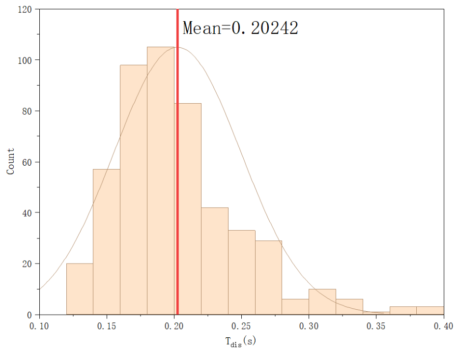
It is asserted that, in accordance with the statistical framework, a multi-variable Monte Carlo simulation is to be executed, encompassing 500 iterations. As illustrated in Figure 12, the resultant discharge times adhere to a well-defined normal distribution. The statistical mean μ t d i s of the discharge time is 0.203 s, with a standard deviation σ t d i s of 0.047 s. The detailed statistical histogram reveals that the probability of the discharge time exceeding the 2.0 s safety limit is mathematically negligible.
Furthermore, transient waveform monitoring during the 500 iterations confirmed that the random injection of L did not induce catastrophic high-frequency ringing or undamped oscillations. The localized gate-source clamping networks D k 1 and series damping resistors R k 1 effectively absorbed the transient L d i / d t spikes, ensuring the cascaded MOSFETs remained strictly within their dynamic Safe Operating Area (SOA).

4. Experimental Verification

4.1. Experimental Setup and Prototype Implementation

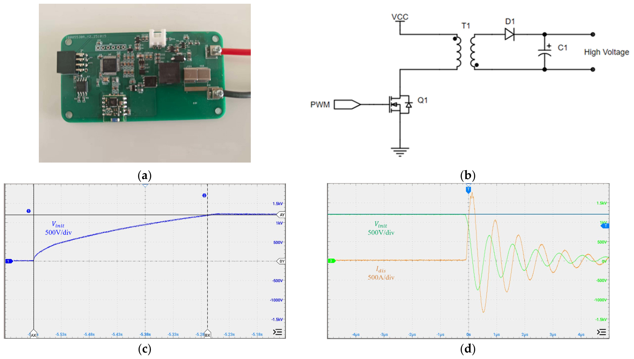
In order to experimentally validate the performance and reliability of the proposed safety discharge topology, a compact high-voltage short pulse generator was developed to serve as the application testbed, as shown in Figure 13. This system generates the requisite high-voltage bus potential, thereby establishing the operational environment for the discharge circuit.
As illustrated in Figure 13a, the fabricated hardware assembly comprises multiple components. This system integrates low-voltage control logic with a high-voltage boost stage within a minimized PCB footprint. The core high-voltage generation section employs a flyback converter topology, as illustrated in the simplified schematic shown in Figure 13b. The application of a PWM signal to the primary-side switch Q1 results in an augmentation of the low-voltage input through transformer T1, which is subsequently rectified by diode D1. This process facilitates the charging of the energy storage capacitor C1; all relevant components are surface-mount devices to achieve a compact design. Figure 13c offers experimental validation of the dynamic boost characteristics of this stage. The charging curve demonstrates that the bus voltage successfully attains the target high-voltage level of 1200 V within a charging time of 0.3 s. Upon completion of the charging cycle, the system can be programmed to generate the high-intensity short pulse. The short-circuit discharge waveform is illustrated in Figure 13d. The resulting output exhibits a rapid voltage collapse accompanied by a peak discharge current of approximately 1500 A (with typical ringing, a characteristic of underdamped RLC pulse discharge). This test platform effectively provides the extreme electrical stresses necessary to verify the robustness and fast response characteristics of the integrated safety discharge circuit.
Subsequent to the simulation analysis, a hardware prototype of the proposed safety discharge topology was fabricated in order to verify its practical performance. The selection of critical components, including the depletion-mode MOSFETs, the voltage-balancing network, and the photovoltaic driver, adheres to the design specifications listed in Table 3.
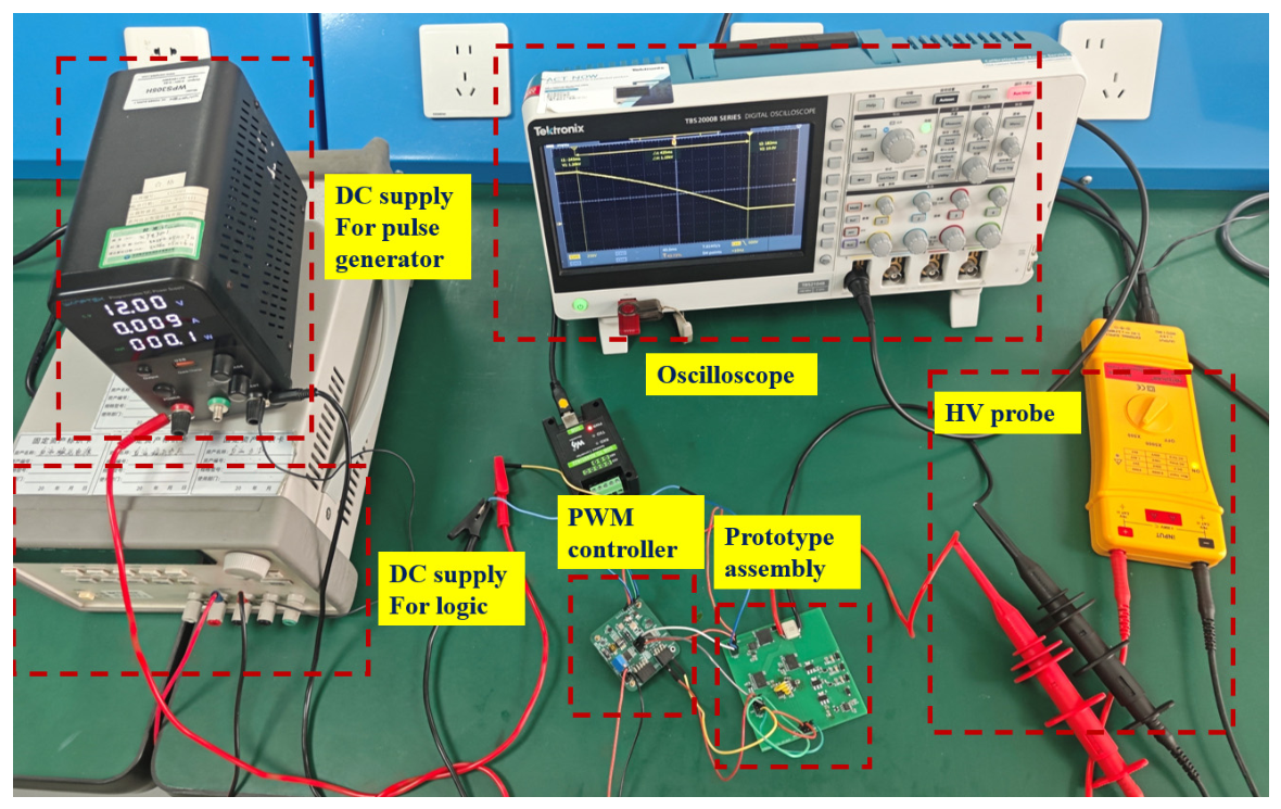
The experimental test bench is illustrated in Figure 14. The configuration of the setup is designed to assess the circuit’s performance under actual high-voltage conditions.
  • Prototype Assembly: The discharge circuit is implemented on a custom printed circuit board (PCB) and integrated with the compact pulse generator described in Section 4.1.
  • The process of signal synchronization is defined as follows: A dedicated pulse-width modulation (PWM) controller orchestrates the system timing. The system generates control signals to manage the charging phase (via the pulse generator’s flyback circuit) and the discharging phase (via the proposed topology’s optocoupler interface), ensuring a transition between blocking and discharge modes.
  • Data Acquisition: The transient voltage response across the energy storage capacitor is monitored using a digital oscilloscope (Tektronix TBS2104B from Tektronix, Beaverton, OR, USA) equipped with a 500:1 high-voltage passive probe (PINTEON PT-5240 from Guangzhou PINTEON, China).
  • Power Source: The regulated DC power supplies (Agilent E3632A from Agilent Technologies, Santa Clara, CA, USA and WANPTEK WPS305H from Shenzhen Guce Electronic Technology, Shenzhen, China) provide the low-voltage input for the pulse generator’s boost stage and the logic controller separately.

4.2. Comparative Discharge Performance and Programmability

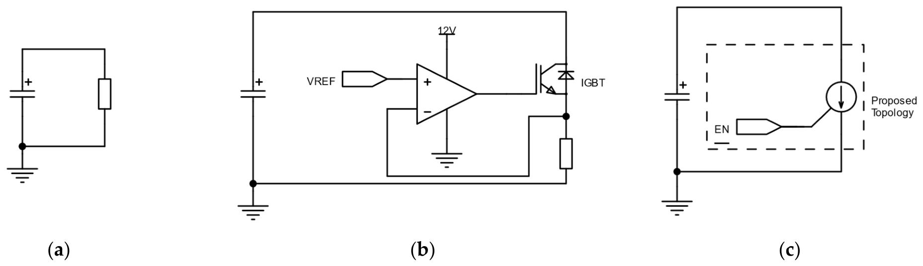
To comprehensively evaluate the effectiveness of the proposed architecture, an experimental comparative analysis was conducted. As illustrated in Figure 15, based on the analysis of the discharge mechanism, we designed three distinct discharge configurations for the testbed and compared them under identical high-voltage load conditions:
  • Passive Resistor: This approach is considered a standard passive discharging method. In order to guarantee that the velocity and efficacy of the high-voltage charging process would not be adversely affected by excessive continuous leakage current, the passive bleeder resistance was selected to match the resistance value of the static voltage-balancing network utilized in the proposed topology, specifically 100 MΩ.
  • Active IGBT Bleeder: This active configuration utilizes a 1600 V power IGBT as the primary discharging device, coupled with an operational amplifier that functions as the constant-current control unit. In order to ensure an evaluation of performance under equivalent conditions, the input of the operational amplifier was calibrated so that the IGBT’s discharge current matched the discharge rate of the proposed circuit. This configuration is contingent upon a continuous 12 V auxiliary power supply to function optimally.
  • Proposed Topology: The self-biased cascaded architecture developed in this study. In order to validate the constant-current discharge capability and the programmability of the proposed topology, a series of discharge tests were conducted by varying the current-limiting resistor R c . The selection of resistance values was made to encompass a broad spectrum of discharge currents, ranging from 4.7 kΩ to 220 Ω.
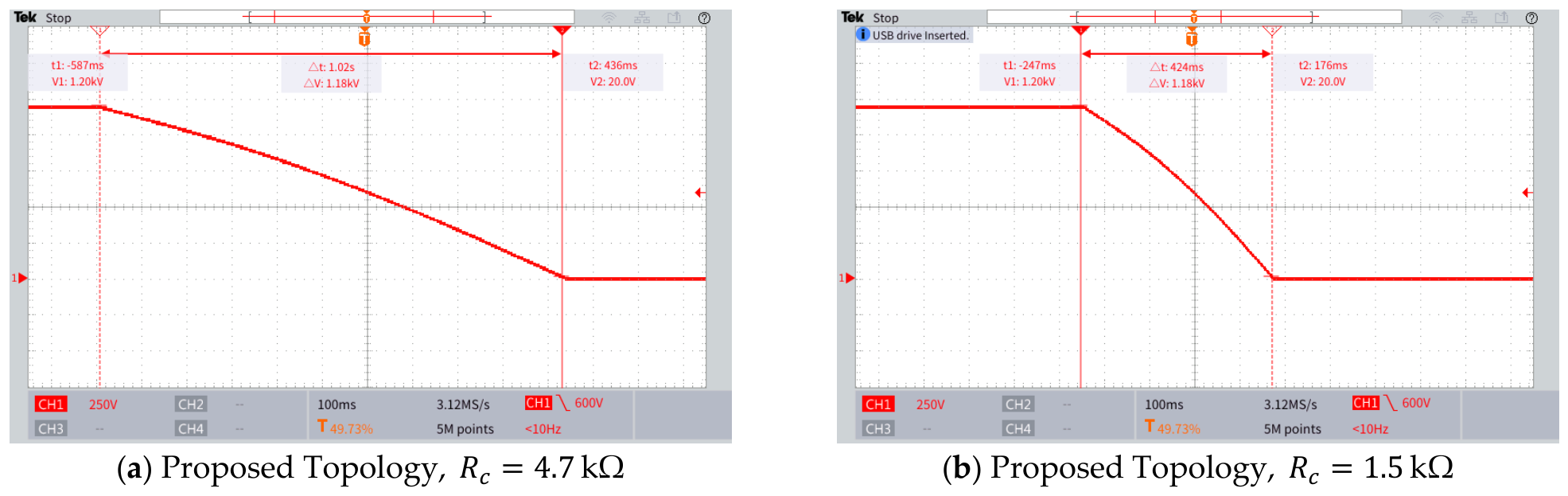
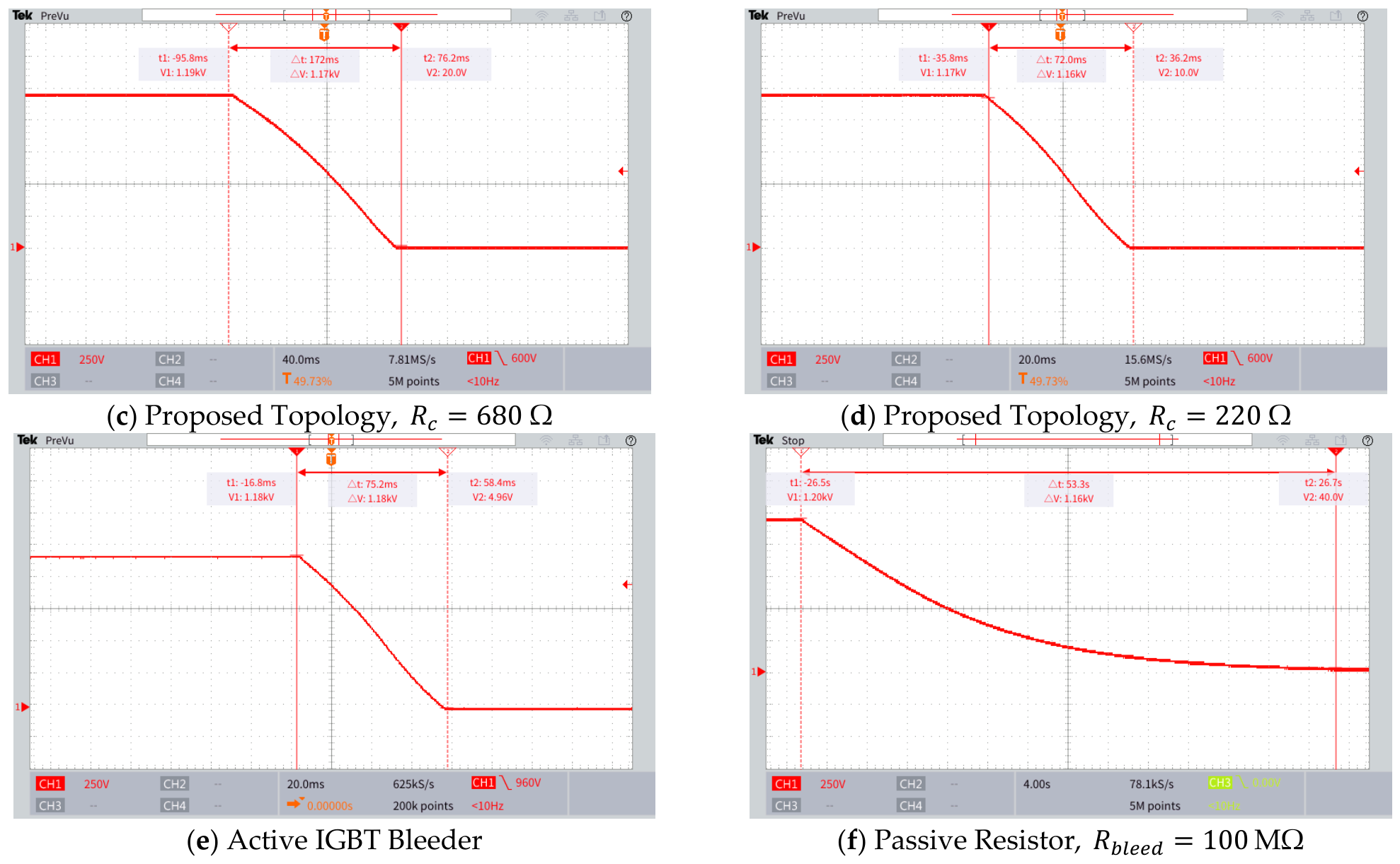
The comparative oscilloscope waveforms of the bus voltage decay profiles are presented in Figure 16, providing an experimental validation of the discharge methods. As illustrated in Figure 16a–d, the proposed topology demonstrates a linear voltage decline across all tested configurations. This linearity serves to confirm the constant-current discharge capability that is inherent to the cascaded depletion-mode NMOS architecture. In addition, the subfigures illustrate the programmability of the proposed circuit. By adjusting the source limiting resistor R c , from 4.7 kΩ down to 220 Ω, the discharge time can be flexibly tuned from 1.02 s to 72.0 ms.
In order to underscore the merits of the proposed topology, a comparative analysis was conducted against both traditional active and passive bleeder circuits. While the active IGBT bleeder (Figure 16e) also achieves a linear, constant-current discharge with a comparable speed of 75.2 milliseconds, its flaw lies in its power dependency. In the context of a total power loss scenario, the active IGBT bleeder is rendered non-functional. In contrast, the proposed topology employs a 3.3 V control signal to ensure the maintenance of the blocking state during standard operation. In the event of power loss, the depletion-mode devices inherently revert to their normally-on state, executing the safety discharge entirely without external power. Finally, the traditional passive bleeder (Figure 16f) is characterized by a pronounced exponential long-tail decay, dictated by the RC time constant. Utilizing a 100 MΩ resistor necessitates a duration of 53.3 s to attain a safe voltage limit.
In order to provide a quantitative assessment, the voltage drop Δ V and the discharge time T d i s were extracted from the oscilloscope cursors in Figure 16. The experimental average discharge current I d i s was subsequently determined through the application of Equation (8). The measured data and calculated currents, which summarize the superior speed and power-loss resilience of the proposed topology, are presented in Table 6.
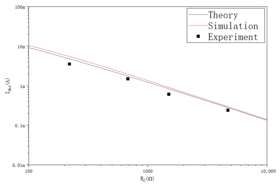
In order to validate the proposed constant-current discharge mechanism, a comparative analysis was performed among theoretical models, simulations, and hardware measurements. As illustrated in Figure 17, the discharge current I d i s is presented as a function of the programming resistor R c . The downward trajectory observed in both the theoretical derivation (Equation (6)) and the simulation results confirms the fundamental inverse relationship between the programming resistance and the regulated current when the depletion-mode MOSFETs operate in the saturation region.
An analysis of the experimental data (black squares) reveals trend consistency with the ideal models. However, a slight but systemic downward deviation is observable, where the experimental discharge currents are marginally lower than the theoretical predictions. This negative offset can be attributed to several practical physical factors inherent in the hardware assembly:
  • Parasitic Series Resistance: The theoretical model posits an ideal R c . In the fabricated prototype, the equivalent series resistance of the high-voltage capacitor, the PCB trace impedance, and the contact resistances of the wiring introduce an additive parasitic term. This increased effective source resistance inevitably strengthens the negative feedback loop of the MOSFET, further restricting the steady-state discharge current and pulling the experimental data points downward.
  • Device Parameter Spread: The discrete BSP135 MOSFETs employed in the prototype inherently manifest manufacturing tolerances in critical parameters, such as the zero-gate-voltage drain current and pinch-off voltage, which may deviate slightly from the standardized SPICE model parameters.
  • Capacitor Tolerance Propagation: As the experimental average current is calculated indirectly from the measured discharge time, the tolerance in the physical high-voltage capacitor will mathematically propagate as a lower calculated current.

4.3. Repeatability Testing and Statistics

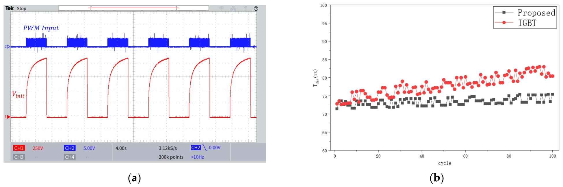
To evaluate the statistical consistency and repeatability of the physical hardware’s endurance, an automated cyclical test was performed. The PWM controller alternated continuously between the high-voltage charging phase and the active discharging phase for 100 cycles. The tests were conducted using the R c = 220 Ω configuration to enable quick discharging.
Figure 18a shows a portion of the continuous oscilloscope recording from this automated test. It demonstrates reliable mode transitions without triggering ringing or system failure. To establish a performance benchmark, a 100-cycle endurance test was conducted on the proposed cascaded topology and the IGBT-based active bleeder.
The discharge time T d i s for each cycle was recorded and plotted in Figure 18b. The extracted data reveals two behavioral trends.
  • Proposed topology: The discharge time was uniform across 100 iterations. The physical hardware yielded a mean of 73.36 ms and a standard deviation of 0.98 ms.
  • IGBT bleeder: The active IGBT circuit demonstrated pronounced upward thermal drift. Over 100 cycles, the discharge time increased from approximately 73 ms to over 82 ms.

4.4. Robustness Against Parameter Dispersion

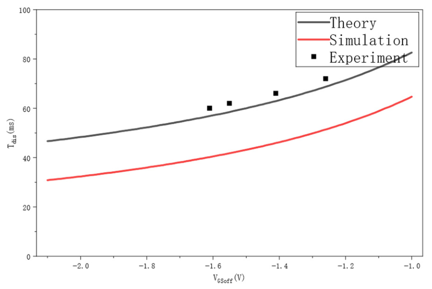
A component replacement experiment was conducted to validate the theoretical sensitivity models and prove the circuit’s robustness against manufacturing dispersion. Standard commercial depletion-mode MOSFETs exhibit variation in their pinch-off voltage V G S o f f from batch to batch. To evaluate the impact of this variation, MOSFET samples with different V G S o f f values were systematically installed in the Q 1 position of the prototype.
The discharge time T d i s was recorded for each sample and plotted alongside the theoretical prediction and the parametric sweep simulation results. As shown in Figure 19, the experimental measurements align somewhat with the theoretical curve. The discharge time T d i s varied from 60.0 ms to 72.0 ms as the V G S o f f fluctuated from −1.61 V to −1.26 V.
Notably, there is a systematic deviation between the simulation curve and the physical/theoretical data. This discrepancy can be attributed to the difference between the software model of the BSP135 device and its actual physical components. The software model’s idealized transconductance and default saturation characteristics differ from those of the real-world hardware, resulting in a faster simulated discharge rate. However, the nonlinear trend across all three curves verifies the core self-biasing mechanism.

4.5. Thermal Stability Testing

A thermal chamber test was conducted to evaluate the thermal stability and validate the theoretical temperature-dependent characteristics of the proposed topology. The prototype was placed in a temperature testing chamber and the temperature was systematically increased from 25 °C to 80 °C. The discharge time T d i s was measured at each temperature checkpoint. The experimental results are summarized in Table 7.
As the ambient temperature increased to 80 °C, the discharge current I d i s decreased from 3.54 mA to 2.85 mA. This led to a proportional extension of the discharge time T d i s . This empirical data aligns with the dynamic thermal equilibrium. In the strong-inversion saturation regime, which is maintained by the self-biasing resistor R c , the reduction in carrier mobility μ T due to enhanced acoustic phonon scattering strictly dominates the threshold voltage shift. Consequently, the overall discharge current intrinsically exhibits a negative temperature coefficient. This characteristic serves as a self-limiting safety mechanism that reduces dynamic power dissipation at elevated temperatures.
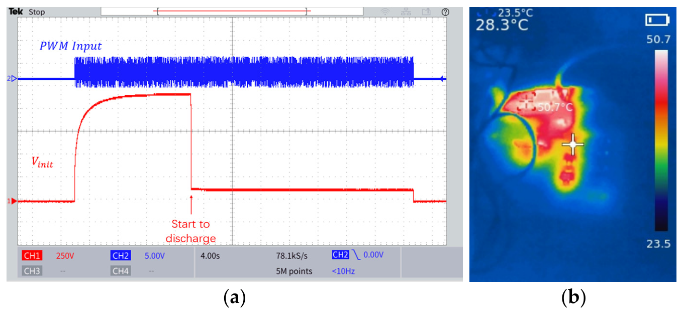
In addition to the ambient temperature sweep, an extreme operational fault condition was evaluated in which both the high-voltage charging module and the safety discharge circuit were engaged simultaneously. As illustrated in Figure 20a, the proposed topology effectively overpowers the charging circuit, ensuring the bus voltage is safely clamped at a stable intermediate level, rather than inducing a thermal breakdown. The cascaded MOSFETs effectively function within the linear region, continuously dissipating the incoming power until the PWM signal is terminated.
Furthermore, an infrared thermal imager was used to evaluate the steady-state thermal distribution during this high-dissipation equilibrium. Figure 20b shows that the maximum PCB surface temperature was 50.7 °C when operated at an ambient temperature of 23.5 °C. These results confirm that the prototype can safely navigate the high-stress region without violating the devices’ Safe Operating Area (SOA) limits.

5. Discussion

The experimental outcomes presented in this study corroborate the working hypothesis that a self-biased, cascaded depletion-mode MOSFET topology can effectively function as a reliable high-voltage safety discharge mechanism. The physical robustness of the theoretical models has been validated through a systematic evaluation of the prototype. This evaluation included nominal operation, cycle endurance testing, parameter replacement, and ambient temperature sweeps.
In order to quantitatively assess the advantages of the proposed architecture, an experimental benchmarking analysis was performed against two standard solutions: an active enhancement-mode bleeder (utilizing a 1600 V IGBT and operational amplifier) and a passive resistive bleeder. A synopsis of the comparative performance is presented in Table 8.
As indicated in Table 8, passive bleeders are distinguished by their exponential decay tails and consequent protracted safety hazards, which contravene the imperative for rapid-discharge safety measures. While the passive method is characterized by its fail-safe nature, its discharge speed density is significantly low. In contrast, the IGBT active bleeder aligns with the linear decay and velocity of the proposed topology. However, it introduces vulnerabilities, such as its dependence on an auxiliary supply, rendering it ineffective in scenarios of power loss.
The proposed self-biased topology has been demonstrated to effectively address these trade-offs. It is imperative to note that the constant discharge current is governed by the source feedback resistor R c . This behavior is consistent with the Shockley equation for depletion-mode devices operating in the saturation region, as evidenced by the linearity of the experimental voltage–time profiles. The elimination of auxiliary power supplies and external gate drivers results in a minimized physical footprint. This, in turn, yields an approximate high discharge speed density of 1344 V/s/cm3.
Additionally, the programmability of the discharge rate, as demonstrated by the parametric variation of R c , offers a distinct advantage over fixed-resistance solutions. This capability enables engineers to optimize the balance between discharge speed and thermal dissipation, tailored to the specific energy storage constraints of the system under design. Of particular significance is the transition from the blocking mode to the discharge mode, which is initiated by the removal of the logic control signal. This transition serves to validate the fail-safe functionality of the design. This activation protocol is designed to ensure that the system automatically transitions to a safe state in the event of a power loss or control failure.
The proposed circuit provides an effective methodology by utilizing a cascaded configuration. This configuration enables the use of depletion-mode MOSFETs with breakdown voltages significantly lower than the total bus voltage as primary discharge devices. This architectural approach circumvents the necessity of employing bulky, large-packaged ultra-high-voltage switching devices, thereby substantially reducing the physical volume and cost of the safety discharge circuit. Consequently, the topology is well-suited for integration into compact, miniaturized pulse generators.
The demonstration of the versatility of the approach under consideration is facilitated by Table 9, which provides the theoretical design parameters for the implementation of the proposed discharge circuit with various pulse generators as reported in the extant literature. However, it is imperative to acknowledge that the specific control logic and targeted discharge speed must be meticulously tailored and adjusted according to the precise design objectives and energy constraints inherent to the individual pulse generator system.
While the current study validates the self-biased discharge mechanism, future research endeavors will focus on the following directions to further expand the topology’s capabilities:
  • Application of SiC Devices: Investigating the implementation of the proposed topology using Silicon Carbide (SiC) depletion-mode devices. This will enable the circuit to accommodate higher bus voltages, scaling into the tens of kilovolts regime, by leveraging the superior high-voltage and thermal characteristics of wide-bandgap materials.
  • Verification of Higher-Stage Scaling: The construction and experimental validation of circuits with a considerably higher number of cascaded stages is imperative. This is critical to further verify the scalability of the voltage-balancing network and the robustness of the topology under ultra-high-voltage string configurations.
  • System-Level Integration and Comprehensive Testing: Developing an integrated design within a miniaturized pulse generator system. This will be coupled with more comprehensive environmental testing and extended long-term reliability testing to thoroughly assess the operational endurance of the topology in real-world field conditions.
  • Component-Level Integration: Pursuing the integrated design of the repeated components within each cascaded stage. By combining the MOSFETs and the balancing passive networks, the physical volume and total component count can be further minimized, maximizing the discharge speed density for ultra-compact applications.

6. Conclusions

In this study, a novel fail-safe high-voltage safety discharge topology utilizing cascaded depletion-mode NMOS transistors was proposed, theoretically analyzed, and experimentally validated. The system’s design incorporates a self-biased architecture in conjunction with a photovoltaic-output optocoupler, ensuring an automatic, constant-current discharge in the event of a loss of control signals or system power. This configuration fulfills the requirements for fail-safe operation, bypassing the need for an auxiliary power supply.
A series of experimental evaluations were conducted on a 1200 V, 220 nF short pulse generator testbed. The proposed topology consistently achieved a linear voltage decay, successfully discharging the high-voltage load to safe levels in as little as 60.0 ms. The adjustment of the current-limiting resistor R c enables programming of the discharge current and the resultant discharge time. Additionally, the cascaded design effectively distributed high-voltage stress across small-scale packaging devices, thereby eliminating the necessity for bulky ultra-high-voltage switches. This configuration yielded a compact physical footprint (31 × 48 × 10 mm3)—a substantial enhancement over passive bleeders, which exhibited exponential decay and required 53.3 s to discharge the same load.
The proposed circuit demonstrated robust statistical consistency, parameter desensitization, and thermal stability. During a continuous endurance test, the prototype demonstrated a high degree of repeatability in its discharge time, with a mean of 73.36 milliseconds and a minimal standard deviation of 0.98 milliseconds. Thermal chamber evaluations from 25 °C to 80 °C empirically validated that the self-biasing mechanism intrinsically provides a negative temperature coefficient, safely limiting dynamic power dissipation at elevated temperatures. In scenarios involving concurrent charging and discharging, the prototype demonstrated its capacity to safely clamp the bus voltage, with the maximum surface temperature reaching a stabilized level of 50.7 °C.
This self-biased cascaded topology was demonstrated to provide a reliable, compact, and cost-effective solution for rapid energy depletion in high-voltage applications. By surmounting the constraints imposed by passive bleeders and conventional active switches, it shows potential for integration into miniaturized pulse generators. Subsequent research endeavors will investigate the scaling of the architecture to tens of kilovolts through the utilization of SiC depletion-mode devices and the advancement of its component-level integration for ultra-compact systems.

Author Contributions

Conceptualization, Q.L. and X.C.; methodology, Q.L.; software, X.C.; validation, Q.L., X.C. and Y.W.; formal analysis, Y.N.; investigation, Q.L. and H.Z.; resources, H.Z.; data curation, X.C.; writing—original draft preparation, Q.L.; writing—review and editing, Y.N. and X.C.; visualization, Q.L. and H.Z.; supervision, H.Z.; project administration, X.C. and Y.N.; funding acquisition, Q.L. and H.Z. All authors have read and agreed to the published version of the manuscript.

Funding

This research received no external funding.

Data Availability Statement

The raw data supporting the conclusions of this article will be made available by the authors on request.

Conflicts of Interest

The authors declare no conflicts of interest.

Abbreviations

The following abbreviations are used in this manuscript:
NMOSN-type Metal-Oxide-Semiconductor
ACAlternating Current
DCDirect Current
MOSFETMetal-Oxide-Semiconductor Field-Effect Transistor
IGBTInsulated Gate Bipolar Transistor
SiCSilicon Carbide
IECInternational Electrotechnical Commission
ISOInternational Organization for Standardization
EVElectric Vehicle
BJTBipolar Junction Transistor
RCResistor-Capacitor
SMPSSwitched-Mode Power Supply
SOASafe Operating Area
LEDLight Emitting Diode
GaAlAsGallium Aluminum Arsenide
PSIMPower Simulation
PCBPrinted Circuit Board
PWMPulse Width Modulation
HVHigh-Voltage
LDOLow-Dropout Regulator
GaNGallium Nitride

References

  1. Mankowski, J.; Kristiansen, M. A Review of Short Pulse Generator Technology. IEEE Trans. Plasma Sci. 2000, 28, 102–108. [Google Scholar] [CrossRef]
  2. Farajzadeh, A.; Khalaj Monfared, K.; Abbas Shayegani Akmal, A.; Bagheri, A. A High-Voltage Flat-Top Pulse Generator with Sub-Nanosecond Rise Time Based on Avalanche Transistors. IEEE J. Emerg. Sel. Top. Power Electron. 2025, 13, 4882–4892. [Google Scholar] [CrossRef]
  3. Chen, S.; Cheng, X.; Wang, S.; Wang, Y.; Liang, J. 3-MHz High-Voltage Pulse Generator with Novel Multilevel LC Resonant Network for Adjustable Pulsewidth. IEEE Trans. Power Electron. 2025, 40, 1012–1022. [Google Scholar] [CrossRef]
  4. Korotkov, S.V.; Aristov, Y.V.; Zhmodikov, A.L. A High Voltage Diode-Transistor Generator of Nanosecond High Voltage Pulses. Instrum. Exp. Tech. 2020, 63, 53–57. [Google Scholar] [CrossRef]
  5. Mauricio Vélez Salazar, F.; Patiño Arcila, I.D. In-Silico Research on the Effects of Variable Voltage Pulse Protocols on the Cell Survival and Permeabilization Fractions in Electroporated Cancerous Tissues. Microchem. J. 2024, 203, 110736. [Google Scholar] [CrossRef]
  6. Pirc, E.; Miklavčič, D.; Uršič, K.; Serša, G.; Reberšek, M. High-Frequency and High-Voltage Asymmetric Bipolar Pulse Generator for Electroporation Based Technologies and Therapies. Electronics 2021, 10, 1203. [Google Scholar] [CrossRef]
  7. Cui, X.; Shen, J.; Zhou, Y.; Zhu, X.; Zhou, R.; Zhou, R.; Fang, Z.; Cullen, P.J. Nanosecond Pulse-Driven Atmospheric-Pressure Plasmas for Polymer Surface Modifications: Wettability Performance, Insulation Evaluation and Mechanisms. Appl. Surf. Sci. 2022, 597, 153640. [Google Scholar] [CrossRef]
  8. Herashchenko, S.S.; Makhlai, V.A.; Garkusha, I.E.; Petrov, Y.V.; Aksenov, N.N.; Kulik, N.V.; Yelisyeyev, D.V.; Shevchuk, P.B.; Volkova, Y.E.; Merenkova, T.M.; et al. Features of Modifications in the Re-Solidified Surfaces of Advanced Materials Due to High-Power Plasma Pulses. Probl. At. Sci. Technol. 2023, 15–20. [Google Scholar] [CrossRef]
  9. Ariztia, L.; Ibrahimi, N.; Zhabin, A.; de Ferron, A.S.; Rivaletto, M.; Martinod, E.; Bertrand, V.; Novac, B.; Pécastaing, L. A High-Power Electromagnetic Source for Disabling Improvised Explosive Devices. High Volt. 2024, 9, 403–409. [Google Scholar] [CrossRef]
  10. Karcz, K.; Mierczyk, Z.; Kalinowski, A. Directed Energy Weapons: Dissecting Effects and Potential Use. In Proceedings of the 2024 International Radar Symposium (IRS), Wroclaw, Poland, 2–4 July 2024; pp. 183–187. [Google Scholar]
  11. Achour, Y.; Starzyński, J.; Jakubiuk, K. New Architecture of Solid-State High-Voltage Pulse Generators. Energies 2022, 15, 4823. [Google Scholar] [CrossRef]
  12. Achour, Y.; Starzynski, J.; Kasprzycka, W.; Trafny, E. Compact Low-cost High-voltage Pulse Generator for Biological Applications. Int. J. Circuit Theory Appl. 2019, 47, 1948–1962. [Google Scholar] [CrossRef]
  13. Kasri, N.F.; Piah, M.A.M.; Adzis, Z. Compact High-Voltage Pulse Generator for Pulsed Electric Field Applications: Lab-Scale Development. J. Electr. Comput. Eng. 2020, 2020, 6525483. [Google Scholar] [CrossRef]
  14. Wang, L.; Zhang, Z.; Liu, Q.; Zhang, T. A Solid-State Pulse Generator Based on Multilayer Ceramic Capacitors and Insulated Gate Bipolar Transistors. Rev. Sci. Instrum. 2020, 91, 054703. [Google Scholar] [CrossRef]
  15. Gonzalez, J.O.; Wu, R.; Jahdi, S.; Alatise, O. Performance and Reliability Review of 650 V and 900 V Silicon and SiC Devices: MOSFETs, Cascode JFETs and IGBTs. IEEE Trans. Ind. Electron. 2020, 67, 7375–7385. [Google Scholar] [CrossRef]
  16. Baliga, B.J. Silicon Carbide Power Devices: Progress and Future Outlook. IEEE J. Emerg. Sel. Top. Power Electron. 2023, 11, 2400–2411. [Google Scholar] [CrossRef]
  17. Palneedi, H.; Peddigari, M.; Hwang, G.-T.; Jeong, D.-Y.; Ryu, J. High-Performance Dielectric Ceramic Films for Energy Storage Capacitors: Progress and Outlook. Adv. Funct. Mater. 2018, 28, 1803665. [Google Scholar] [CrossRef]
  18. Fan, B.; Zhou, M.; Zhang, C.; He, D.; Bai, J. Polymer-Based Materials for Achieving High Energy Density Film Capacitors. Prog. Polym. Sci. 2019, 97, 101143. [Google Scholar] [CrossRef]
  19. Pan, Z.; Cheng, X.; Chen, R.; Zhang, H.; Li, R.; Zhang, R.; Qian, B. A Repetitive High Voltage Pulse Generator Based on a Novel Racetrack Blumlein Type Pulse Forming Line. Rev. Sci. Instrum. 2025, 96, 104705. [Google Scholar] [CrossRef]
  20. Ma, J.; Yao, C.; Yu, L.; Li, C.; Liu, C.; Zhao, L.; Dong, S. Compact Nanosecond Pulse Generator Based on Distributed Inductive Energy Storage of Twisted Pair Wire. IEEE Trans. Power Electron. 2025, 40, 1111–1122. [Google Scholar] [CrossRef]
  21. Achour, Y.; Starzynski, J.; Łasica, A. Compact Nanosecond Pulse Generator Based on IGBT and Spark Gap Cooperation. Bull. Pol. Acad. Sci. Tech. Sci. 2020, 68, 377–388. [Google Scholar] [CrossRef]
  22. Ranjan, A.; Abhishek, A.; Kumar, N.; Verma, B.K. Review of Nanosecond Pulse Generator with High-Power Switching Devices. IEEE Trans. Electron Devices 2024, 71, 5165–5176. [Google Scholar] [CrossRef]
  23. Pachowicz, K. High-Voltage Power Supply for High Repetitive Rate Marx Generator with Quasi-Resonant Zero-Current Switching Transistor Control Algorithm. Energies 2022, 15, 6902. [Google Scholar] [CrossRef]
  24. Raju, S.; Kularatna, N.; Wilson, M. Supercapacitor Based Adjustable High Power Pulse Generator for Medical Research Applications. In Proceedings of the IECON 2023-49th Annual Conference of the IEEE Industrial Electronics Society, Singapore, 16–19 October 2023; pp. 1–6. [Google Scholar]
  25. Zhu, G.; Dong, J.; Grazian, F.; Bauer, P. A Hybrid Modulation Scheme for Efficiency Optimization and Ripple Reduction in Secondary-Side Controlled Wireless Power Transfer Systems. IEEE Trans. Transp. Electrif. 2025, 11, 6840–6853. [Google Scholar] [CrossRef]
  26. Wang, Y.; Bian, Q.; Li, Z.; Jiang, S. Research of High-Voltage Pulse Generator Based on Marx Circuit and Pulse Transformer. IEEE Trans. Plasma Sci. 2025, 53, 1250–1257. [Google Scholar] [CrossRef]
  27. Jin, S.; Han, W.; Zhang, X.; Zhang, R.; Zhu, L.; Deng, Q.; Xu, S.; Yang, Y. Improved Marx Pulse Generator with Auxiliary Trigger Topology (2022). IEEE Trans. Power Electron. 2023, 38, 5716–5725. [Google Scholar] [CrossRef]
  28. Zhao, Y.; Xie, W.; Jiang, J.; Chen, L.; Feng, S.; Wang, M.; Wang, Z. Replacement of Marx Generator by Tesla Transformer for Pulsed Power System Reliability Improvement. IEEE Trans. Plasma Sci. 2019, 47, 574–580. [Google Scholar] [CrossRef]
  29. Piwowarski, K. Comparison of photoconductive semiconductor switch parameters with selected switch devices in power systems. Opto-Electron. Rev. 2020, 28, 74–81. [Google Scholar] [CrossRef]
  30. Zhang, G.; Cao, R.; Li, P. Comparison of Magnetic Field Characteristics Produced by Three-Electrode Spark Gap Switch and Thyristor Switch in Power Pulsed Systems. IEEE Trans. Plasma Sci. 2019, 47, 5172–5179. [Google Scholar] [CrossRef]
  31. Zhuge, Y.; Liang, J.; Fu, M.; Long, T.; Wang, H. Comprehensive Overview of Power Electronics Intensive Solutions for High-Voltage Pulse Generators. IEEE Open J. Power Electron. 2024, 5, 1–20. [Google Scholar] [CrossRef]
  32. Vats, P.; Singh, B. Development of a Miniature Compulsator for High-Current Pulsed Power Systems. IEEE Trans. Plasma Sci. 2025, 53, 3850–3857. [Google Scholar] [CrossRef]
  33. Lele, S.; Kuykendal, M. A Hazard-Based Approach to Product Safety Assessment. In Proceedings of the 2019 IEEE Symposium on Product Compliance Engineering (SPCE Austin), Austin, TX, USA, 11–12 November 2019; pp. 1–4. [Google Scholar]
  34. Roziskulov, S.S.; Vinnychenko, D.V.; Suprunovska, N.I. Interdependent Transient Processes in Circles of Bipolar Discharge Pulse Current Generator with R-L-C Load and Limited Positive Voltage Feedback. Tech. Electrodyn. 2025, 3–10. [Google Scholar] [CrossRef]
  35. Caskey, L.; Cohen, I.J.; Lamberson, A.; Walker, J.; Elliott, C.; Rader, M. Pulsed Discharge Testing of High Voltage Energy Storage Devices. In Proceedings of the 2023 IEEE Pulsed Power Conference (PPC), San Antonio, TX, USA, 25–29 June 2023; pp. 1–3. [Google Scholar]
  36. Gong, C.; Hu, Y.; Gao, J.; Wu, Z.; Liu, J.; Wen, H.; Wang, Z. Winding-Based DC-Bus Capacitor Discharge Technique Selection Principles Based on Parametric Analysis for EV-PMSM Drives in Post-Crash Conditions. IEEE Trans. Power Electron. 2021, 36, 3551–3562. [Google Scholar] [CrossRef]
  37. Gong, C.; Liu, J.; Han, Y.; Hu, Y.; Yu, H.; Zeng, R. Safety of Electric Vehicles in Crash Conditions: A Review of Hazards to Occupants, Regulatory Activities, and Technical Support. IEEE Trans. Transp. Electrif. 2022, 8, 3870–3883. [Google Scholar] [CrossRef]
  38. Gong, C.; Hu, Y.; Chen, G.; Wen, H.; Wang, Z.; Ni, K. A DC-Bus Capacitor Discharge Strategy for PMSM Drive System with Large Inertia and Small System Safe Current in EVs. IEEE Trans. Ind. Inform. 2019, 15, 4709–4718. [Google Scholar] [CrossRef]
  39. Zhang, X.; Yang, J. DC-Bus Capacitor Discharge Method Based on Bleeder and Windings for Electric Vehicles in Emergency. IEEE Access 2024, 12, 61949–61958. [Google Scholar] [CrossRef]
  40. Wu, Z.; Su, X.; Zhu, Y.; Xiao, M. DC Link Capacitor Active Discharge by IGBT Weak Short Circuit. SAE Int. J. Adv. Curr. Pract. Mobil. 2019, 01, 1177–1187. [Google Scholar] [CrossRef]
  41. Sezer, M.M.; Norwood, D.; Geiger, J.; Hava, A.M.; Akin, B. An Active Discharge Scheme for DC-Bus Capacitors in EV Powertrain. IEEE Trans. Power Electron. 2025, 40, 16512–16524. [Google Scholar] [CrossRef]
  42. Liu, A.-C.; Hsieh, C.-H.; Langpoklakpam, C.; Singh, K.J.; Lee, W.-C.; Hsiao, Y.-K.; Horng, R.-H.; Kuo, H.-C.; Tu, C.-C. State-of-the-Art β-Ga2O3 Field-Effect Transistors for Power Electronics. ACS Omega 2022, 7, 36070–36091. [Google Scholar] [CrossRef]
  43. Chen, B. Depletion-Mode MOSFET: The Forgotten FET; Supertex Inc.: Sunnyvale, CS, USA, 2015; Available online: https://www.microchip.com/en-us/application-notes/and66 (accessed on 15 May 2026).
  44. Jia, X.; Wang, Y.; Yang, J.; Liu, Y.; Hao, Y.; Han, G. A Compact Model of DC I–V Characteristics for Depleted Ga2O3 MOSFETs. Microelectron. J. 2023, 140, 105920. [Google Scholar] [CrossRef]
  45. Mehrotra, U.; Hopkins, D.C. Methodologies of Cascading to Realize High-Voltage Cascaded Super Cascode Power Switch. IEEE J. Emerg. Sel. Top. Power Electron. 2023, 11, 5853–5862. [Google Scholar] [CrossRef]
  46. Madhusoodhanan, S.; Sabbar, A.; Tran, H.; Lai, P.; Gonzalez, D.; Mantooth, A.; Yu, S.-Q.; Chen, Z. High-Temperature Analysis of Optical Coupling Using AlGaAs/GaAs LEDs for High-Density Integrated Power Modules. Sci. Rep. 2022, 12, 3168. [Google Scholar] [CrossRef] [PubMed]
  47. Rao, X.; Chen, X.; Zhou, J.; Zhang, B.; Alfadhl, Y. Design of a High Voltage Pulse Generator with Large Width Adjusting Range for Tumor Treatment. Electronics 2020, 9, 1053. [Google Scholar] [CrossRef]
  48. Cao, X.; Song, G.; Chen, Y.; Chen, H. Research on Solid-State Linear Transformer Driver Power Source Driving Atmospheric Pressure Plasma Jet Treatment of Epoxy Resin. Energies 2024, 17, 4749. [Google Scholar] [CrossRef]
Figure 1. Composition of the Short Pulse Generator [1,11].
Electronics 15 02346 g001
Figure 2. Schematic diagram of the proposed high-voltage switch topology based on cascaded depletion-mode NMOS transistors with an R-C voltage-balancing network and optical isolation control mechanism.
Electronics 15 02346 g002
Figure 3. Typical transfer (a) and output (b) characteristics of a N-channel depletion-mode MOSFET.
Electronics 15 02346 g003
Figure 4. Schematic of a simple constant current source based on the depletion-mode N-channel MOSFET.
Electronics 15 02346 g004
Figure 5. Equivalent circuit configuration during the Discharge Mode ( V C T R L = 0 ), illustrating the passive turn-on mechanism of the depletion-mode MOSFET stack.
Electronics 15 02346 g005
Figure 6. Equivalent circuit configuration during the Blocking Mode ( V C T R L = High ), showing the active cutoff of Q 1 via optocoupler biasing and the subsequent high-impedance state of the cascaded stack.
Electronics 15 02346 g006
Figure 7. Simulation model of the proposed cascaded high-voltage discharge circuit implemented in PSIM 2025.0 software.
Electronics 15 02346 g007
Figure 8. Simulated transient waveforms during the discharge process ( V i n i t = 1200 V , C l o a d = 220 nF , R c = 1 k Ω ). (a) Voltage decay trajectories of the balancing nodes, showing linear and uniform discharge characteristics. (b) Gate-source voltage V G S variations in the cascaded MOSFETs, illustrating the self-biased constant-current regulation region and the return to the zero-bias conducting state.
Electronics 15 02346 g008
Figure 9. Parametric simulation results showing the programmability of the discharge characteristics by varying R c . (a) Voltage decay profiles, illustrating the adjustable discharge time while maintaining linearity. (b) Discharge current waveforms, demonstrating the precise regulation of the current magnitude via R c .
Electronics 15 02346 g009
Figure 10. Transient response simulation of the mode switching process. The control signal transitions from High to Low at t = 0.5 s . The plot illustrates the immediate activation of the discharge current I d i s (left axis) and the subsequent linear decay of the bus voltage V i n i t (right axis), completing the safety discharge within 0.2 s.
Electronics 15 02346 g010
Figure 11. Parametric sweep simulation results validating the dynamic attenuation of parameter dispersion on the total discharge time T d i s . (a) The effect of varying the pinch-off voltage V G S o f f from 2.1   V   to   1.0   V . (b) The effect of varying the saturation current I D S S from 0.02   A to 0.08   A , highlighting the severely restricted y-axis scale, which empirically proves the negligible impact of I D S S dispersion ( S I D S S T d i s 0.06 ).
Electronics 15 02346 g011
Figure 12. Statistical histogram of the discharge time T d i s obtained from N   =   500 Monte Carlo simulation iterations. The calculated mean discharge time is tightly regulated at 0.203 s.
Electronics 15 02346 g012
Figure 13. Overview of the compact short pulse generator used as the experimental testbed. (a) Photograph of the fabricated hardware assembly. (b) Simplified schematic of the high-voltage boost stage. (c) Measured voltage charging curve (boost characteristic). (d) Captured waveform of the high-voltage pulse output.
Electronics 15 02346 g013
Figure 14. Photograph of the experimental test bench. The setup includes the fabricated prototype connected to the high-voltage load, a regulated DC power supply, a PWM controller for signal synchronization, and a digital oscilloscope with a high-voltage probe for real-time waveform monitoring.
Electronics 15 02346 g014
Figure 15. Three distinct discharge configurations evaluated in the comparative analysis: (a) Passive resistor bleeder; (b) Active IGBT bleeder; (c) Proposed self-biased cascaded topology.
Electronics 15 02346 g015
Figure 16. Oscilloscope waveforms demonstrating the comparative bus voltage decay profiles. The cursors indicate the voltage drop Δ V and the discharge time T d i s .
Electronics 15 02346 g016aElectronics 15 02346 g016b
Figure 17. Comparative analysis of the discharge current I d i s as a function of the current-limiting resistor R c . The plot compares the values calculated from theoretical derivation, simulation results and experimental measurements. To highlight the details, a logarithmic coordinate system was implemented.
Electronics 15 02346 g017
Figure 18. Experimental evaluation of operational repeatability and statistical consistency over 100 charge–discharge cycles. (a) Oscilloscope waveforms capturing the automated continuous cycling of the PWM charging input and the corresponding high-voltage bus discharge V i n i t . (b) Scatter plot comparing the total discharge time T d i s of the proposed topology versus a conventional IGBT active bleeder across 100 cycles.
Electronics 15 02346 g018
Figure 19. Comparative analysis of the total discharge time T d i s under varying pinch-off voltages V G S o f f . The plot overlays the theoretical derivation, the software simulation parametric sweep, and the discrete experimental data points.
Electronics 15 02346 g019
Figure 20. Experimental evaluation of the proposed topology regarding dynamic SOA and thermal stability. (a) Oscilloscope waveforms under an extreme simultaneous charge–discharge fault condition, demonstrating stable voltage clamping. (b) Infrared thermal imaging of the prototype during the continuous fault steady-state, with a maximum recorded temperature of 50.7 °C (ambient 23.5 °C).
Electronics 15 02346 g020
Table 1. Comparison of Passive and Active Discharge Mechanisms for High-Voltage Systems [37].
CategoryDischarge TopologyTopology DescriptionAdditional ComponentsPower Leakage During Blocking ProcessAuxiliary Power
Required During Discharge Process
Limitation
PassiveBleeding ResistorA Resistor in ParallelYesHigh (Continuous V 2 / R b l e e d )NoUncontrollable and Slow
ActiveMotor Winding BleedingMotor Winding Resistance via PWM-Controlled SwitchesNoZeroYesOnly for motors
Current-Limiting BleedingCurrent-Limiting CircuitYesLeak Current of SwitchYesHigh Requirements for Switches
Active Bleeding ResistorPower Switch and Bleeding ResistorYesLeak Current of SwitchYesBulky Resistor
HybridCombinations of the Above Topologies////
Table 2. Summary of Existing Active Discharge Mechanisms in the Literature.
Ref.Discharge TopologyKey ComponentsInitial Voltage V i n i t Energy Storage Capacitance C s t o r e Discharge Time T d i s Circuit SizeAux Input While DischargingApplication
[38]Motor Winding /310 V560 μF3.0 s/d- and q-axis current controlPMSM in EVs
[39]Active Bleeding Resistor + Motor Winding HybridBleeding Resistor Module310 V420 μF1.25 s0.5 kg/60 cm3d- and q-axis current controlPMSM in EVs
[40]Current-Limiting BleedingIGBT Module400 V1000 μF1.2 sNot MentionedPWM signalDC Link Capacitor
[41]Current-Limiting BleedingSiC Switch (TO-247 or Module)1000 V600 μF1 sCompactVariable Gate-Source VoltageEV Powertrain
ProposedCurrent-Limiting BleedingDepletion-Mode NMOS (SOT-223)1200 V220 nF<1 sSingle-Layer PCB with SMT ComponentsNoCompact Pulse Generators
Table 3. Main parameters of the simulation topology.
CategoryParameterSymbolValue
System SpecificationsCapacitance Initial Voltage V i n i t 1200 V
Energy Storage Capacitance C s t o r e 220 nF
Number of Stages N 3
Power Stage (MOSFETs)Depletion-Mode NMOS Q 1 Q n BSP135 (Model)
Balancing NetworkStatic Balancing Resistor R k 2 100 MΩ
Dynamic Balancing Capacitor C k 2 4.7 nF
Control and ProtectionCurrent-Limiting Resistor R c 1 kΩ/Variable
Gate Pull-down Resistor R b 2 MΩ
Gate Protection Zener D k 1 7.5 V
Series Gate Resistor R k 1 880 kΩ
Optocoupler Bias Voltage V b i a s 7 V
Table 4. Detailed simulation parameters for the BSP135 depletion-mode MOSFET.
ParameterValue
Drain-Source Breakdown Voltage B V D S S 600 V
On-State Resistance R d s o n 30 Ω
Threshold Voltage V G S o f f −1.4 V
Transconductance g f s 0.16 S
Capacitance C g s 94.6 pF
Capacitance C g d 3.4 pF
Capacitance C d s 5.1 pF
Diode Forward Voltage V S D 0.78 V
Table 5. Parameter Boundaries and Statistical Distributions for WCCA and Monte Carlo Analysis.
ParameterSymbolNominal ValueWCCA Boundary (for T d i s m a x )Monte Carlo Distribution
Capacitance Initial Voltage V i n i t 1200 V + 5 % Gaussian ( + 5 % , 3 σ )
Energy Storage Capacitance C s t o r e 220 nF + 20 % Gaussian ( 20 % , 3 σ )
Threshold Voltage V G S o f f −1.4 V−1.0 VUniform (−2.1 V to −1.0 V)
Saturation Current I D S S 80 mA20 mAUniform (20 mA to 100 mA)
Static Balancing Resistor R k 2 100 MΩN/AGaussian ( + 5 % , 3 σ )
Dynamic Balancing Capacitor C k 2 4.7 nFN/AGaussian ( + 20 % , 3 σ )
Current-Limiting Resistor R c 1 kΩ + 5 % Gaussian ( + 5 % , 3 σ )
Bus Inductance L b u s 0N/AUniform (20 nH to 100 nH)
Table 6. Summary of experimental discharge data and calculated current.
Discharge MethodAuxiliary Power Input During Blocking ProcessAuxiliary Power Input During Discharge ProcessLimiting ResistorMeasured Voltage Drop Δ V Measured Discharge Time T d i s Calculated Discharge Current I d i s
Proposed Topology3.3 V0 R c = 4.7 k Ω 1.18 kV1.02 s0.24 mA
Proposed Topology3.3 V0 R c = 1.5 k Ω 1.18 kV424 ms0.61 mA
Proposed Topology3.3 V0 R c = 680   Ω 1.17 kV172 ms1.50 mA
Proposed Topology3.3 V0 R c = 220   Ω 1.16 kV72.0 ms3.54 mA
Active IGBT Bleeder012 V/1.18 kV75.2 ms3.45 mA
Active IGBT Bleeder00/Cannot Function
Passive Resistor00 R b l e e d = 100 M Ω 1.16 kV53.3 s4.95 μA (average)
Table 7. Experimental Discharge Characteristics Under Varying Ambient Temperatures.
Ambient TemperatureMeasured Voltage Drop Δ V Measured Discharge Time T d i s Calculated Discharge Current I d i s
25 °C1.16 kV72.0 ms3.54 mA
40 °C1.17 kV76.2 ms3.38 mA
60 °C1.17 kV82.8 ms3.11 mA
80 °C1.18 kV91.0 ms2.85 mA
Table 8. Experimental Benchmarking and Discharge Speed Density Comparison.
Discharge MethodDischarge ProfileMinimum Discharge Time MeasuredAux Power RequiredPrototype Dimensions (Package Info)Discharge Speed Density ρ d i s = v d i s / V e f f Features
Proposed TopologyLinear60.0 ms031 × 48 × 10 mm3
(SOT-223 x3)
1344 V/s/cm3Fail-safe
Active IGBT BleederLinear71.6 ms12 V input30 × 24 × 30 mm3 (TO247-3)775 V/s/cm3Fails without aux power
Passive ResistorExponential53.3 s014 × 10 × 10 mm3 (R2512)16.08 V/s/cm3Passive and uncontrollable
Table 9. Theoretical Design Parameters of the Proposed Discharge Circuit for Various Pulse Generators.
ReferenceApplicationStored Energy Parameters ( V i n i t / C s t o r e )Proposed MOSFET Model ( B V D S S )Stages NTarget I d i s / t d i s
[6]Electroporation4 kV/125 μFIXTA6N100D2 (1200 V)41 A/0.5 s
[47]Tumor Treatment2 kV/20 μFDN2470K4-G (700 V)350 mA/0.8 s
[48]Plasma Jet1 kV/160 nFBSP135 (600 V)21 mA/0.16 s
Disclaimer/Publisher’s Note: The statements, opinions and data contained in all publications are solely those of the individual author(s) and contributor(s) and not of MDPI and/or the editor(s). MDPI and/or the editor(s) disclaim responsibility for any injury to people or property resulting from any ideas, methods, instructions or products referred to in the content.