Article

Memristor-Based Read–Write Interface Design for Neural Networks: A Comparative Study of Linear-Drift and VTEAM Models


College of Mechanical and Electrical Engineering, Central South University, Changsha 410083, China
*
Author to whom correspondence should be addressed.
Electronics 2026, 15(11), 2333; https://doi.org/10.3390/electronics15112333
Submission received: 9 April 2026 / Revised: 13 May 2026 / Accepted: 19 May 2026 / Published: 28 May 2026
(This article belongs to the Special Issue Memristor Device and Memristive System)

Abstract

This paper presents a behavioral-level, pre-silicon analytical co-design framework for memristor read–write interfaces, intended to establish closed-form design rules that subsequently guide SPICE-level and silicon-level realizations. Memristor-based neural hardware requires interfaces that can program resistance states efficiently while suppressing read disturbance, yet existing designs typically rely on empirical tuning without closed-form analytical rules. We close this gap by deriving a single closed-form operating-window inequality ( v on < V rd < v off , V wr V wr min ( T wr ) ) from the VTEAM state equation, embedding it in an Energy–Delay–Accuracy (EDA) cost function, and validating the resulting parameter set hierarchically up to MNIST-scale inference. The main finding is that this analytically derived parameter set simultaneously achieves a 96.08% set-cycle energy saving and 90.6% MNIST top-1 accuracy (1.2% below software baseline) under realistic D2D/C2C variability, with every measured number agreeing with its analytical prediction within 2%. The framework is instantiated with a two-phase over-threshold-write and sub-threshold-read timing strategy together with a mutually exclusive PMOS-NMOS path-isolation topology, evaluated through behavioral-level MATLAB simulation under linear-drift and VTEAM models. Behavioral simulation confirms each analytical bound within 2%: a 13.78× resistance window with 0.008 % cycle-to-cycle drift, 5.01% read-current CV, and 30.94%/96.08% Reset/Set energy savings versus a no-separation baseline. Transistor-level non-idealities (slew rate, charge injection, RTN, retention aging, peripheral overhead) are bounded analytically; full SPICE/silicon validation is identified as immediate follow-up work. These results establish a reusable, analytically grounded reference design that bridges memristive device modeling, circuit-level interface implementation, and neural network-level usability.

1. Introduction

The migration of deep neural network (DNN) inference from cloud to edge has intensified demands on power efficiency and data movement, motivating low-power memristive and analog neural accelerators [1,2,3]. Building on the foundational memristor concept [4,5] and the experimental demonstrations of ref. [6,7], memristors have emerged as promising building blocks for neuromorphic hardware that bypasses the von Neumann memory wall.
Building on this foundation, recent studies have demonstrated the potential of memristor-based neural hardware at multiple abstraction levels. Ye et al. reviewed memristor-based neural network design strategies, Wan et al. reported a fully integrated RRAM-based compute-in-memory chip for edge AI, Aguirre et al. summarized the practical implementation issues and block-level design alternatives of memristive neural hardware, Wang et al. demonstrated a near-threshold memristive computing-in-memory engine for edge intelligence, and An et al. emphasized that memristive AI accelerators must be co-optimized across devices, circuits, and systems [8,9,10,11,12]. More recent reviews further consolidate the device–circuit–system co-design view: Shooshtari et al. [13] survey memristor implementations for in-memory computing and spiking neural networks with explicit emphasis on the crossbar/peripheral interface, while the MetroXRAINE study of ref. [14] reports neural engineering-oriented memristive measurements that complement the present interface-level analysis.
At the circuit level, prior studies span analog memristive applications [15,16,17], hybrid CMOS–memristor neurons [18,19], and 3D-integrated arrays with selectors [20]. These works confirm that read disturbance, write accessibility, path isolation, and array non-idealities must be addressed explicitly at the interface level rather than be left to device behavior alone [21,22,23].

1.1. Motivation and Research Gap

Four issues remain insufficiently resolved. First, a reusable circuit methodology balancing read retention and writing accessibility under standard CMOS constraints is lacking [12,15,16,18]. Second, interface-relevant non-idealities (resistance variation, conductance drift, selector compatibility) are usually discussed as device or array phenomena rather than translated into interface-level operating windows [10,16,22,23,24]. Third, coupling between device-level nonlinearity (e.g., VTEAM threshold kinetics) and circuit-level programming dynamics has rarely been formalized into closed-form design rules. Fourth, most existing interface studies validate only on isolated device cells, leaving propagation to neural network inference accuracy unexplored.
This paper is positioned at the behavioral/model level rather than transistor or fabricated-chip level. The contribution is a pre-silicon analytical reference design: closed-form bounds, an EDA cost function, a topology-level isolation rule, and a hierarchical validation pipeline informing subsequent SPICE-level realization. We do not claim transistor-level performance superiority over fabricated peripheral circuits; instead, we provide the analytical scaffolding that SPICE/silicon studies typically lack. Section 5.5 itemizes transistor-level effects (finite slew rate, charge injection, sense-amplifier overhead, RTN, filament aging) that lie outside the present scope.
Read–write separation per se is not new [10,25,26]. The novelty here lies in three previously missing analytical components. First, prior interface studies do not derive the safe operating window as a closed-form inequality jointly bounded by the VTEAM threshold dead zone and the 90% settling time; here, it is Equation (11). Second, prior studies do not couple separation to an Energy–Delay–Accuracy composite cost (Equation (17)) allowing application-specific rebalancing. Third, prior interface validation typically stops at the single-device level, whereas the present pipeline propagates analytical bounds through Monte Carlo variability and a 784 × 10 MNIST-scale crossbar.

1.2. Contributions of This Work

  • Analytical operating-window model. A closed-form expression for the safe read–write operating window from the VTEAM state equation, bounding read voltage by the threshold dead zone and minimum write voltage by 90% settling time (Equations (7)–(9)).
  • Energy–Delay–Accuracy (EDA) co-optimization model. A unified analytical framework linking cycle energy, programming latency, and state-retention accuracy through VTEAM kinetic parameters (Equations (12)–(17)).
  • Read-disturbance upper-bound analysis. Using sub-threshold kinetics, an analytical upper bound on per-cycle read-disturbance drift (Equation (8)).
  • Asymmetry-aware adaptive pulse-width strategy. Based on measured 1.504× Set/Reset asymmetry, a direction-aware pulse-width allocation rule (Equation (19)).
  • Hierarchical validation from device-to-neural network inference. Four levels: (i) single-device switching and cycle-to-cycle repeatability; (ii) 100-run Monte Carlo with D2D/C2C variation; (iii) a 2 × 2 analog crossbar VMM at a behavioral level; (iv) a 784 × 10 crossbar MNIST-style benchmark, confirming interface-induced weight perturbation keeps accuracy within 1.2% of software baseline.
The remainder is organized as follows. Section 2 analyzes the linear-drift and VTEAM models. Section 3 presents the proposed interface and analytical design rules. Section 4 reports quantitative simulation results. Section 5 discusses comparison and limitations, and Section 6 concludes.

2. Memristor Models and Read–Write Mechanisms

2.1. Fundamental Characteristics and Fingerprint Criteria

A memristor’s terminal current–voltage relationship depends on both applied excitation and the evolution history of an internal state variable [4,5,27]. Conductance can be continuously modulated and retained after programming, making memristors attractive for neural network hardware where conductance encodes synaptic weights [1,2,3,5,6].
Two fingerprint characteristics matter for interface design [4,5]. First, under periodic excitation, a memristor exhibits a pinched hysteresis loop through the origin. Second, as excitation frequency increases, hysteresis area shrinks and response approaches a linear resistor. The pinched hysteresis property requires
v ( t * ) = 0 i ( t * ) = 0 , t * R 0 ,
and the loop area A ( ω ) under sinusoidal excitation v ( t ) = V 0 sin ( ω t ) is
A ( ω ) = C ( ω ) i ( v ) d v ,
where C ( ω ) denotes the closed I-V trajectory over period T = 2 π / ω .
Figure 1 confirms the pinched hysteresis fingerprint required for read–write analysis.

2.2. Comparative Analysis of Linear-Drift and VTEAM Models

The linear-drift model is structurally simple and suited to continuous state evolution, while the VTEAM model introduces explicit threshold conditions and is appropriate for analyzing read–write windows [4,27,28].
The linear-drift model represents the device as a series combination of low- and high-resistance regions with v ( t ) = R ( x ) i ( t ) , R ( x ) = R on x + R off ( 1 x ) , x [ 0 , 1 ] :
d x d t = μ v R on D 2 i ( t ) ,
where μ v is ion mobility, D is device length [4].
The VTEAM model uses polarity-dependent switching conditions [28]:
d x d t = k off v ( t ) v off 1 α off , 0 < v off < v ( t ) , 0 , v on < v ( t ) < v off , k on v ( t ) v on 1 α on , v ( t ) < v on < 0 ,
with x [ x on , x off ] . The piecewise structure defines a dead zone [ v on , v off ] within which the state variable is unchanged—the basis for sub-threshold read retention.
The local resistance sensitivity S R ( x ) d R / d x for the linear-drift model is
S R LD ( x ) = R on R off ,
while for VTEAM with R ( x ) = R on + ( R off R on ) ( 1 x ) γ ,
S R VTEAM ( x ) = γ ( R off R on ) ( 1 x ) γ 1 .
Near the high-resistance boundary, VTEAM exhibits higher sensitivity, implying sharper transitions but greater readout sensitivity.
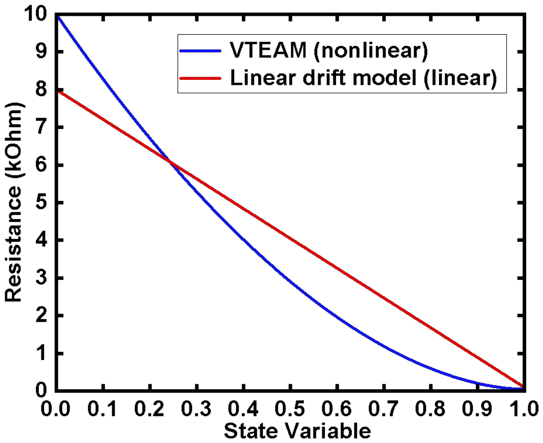
Figure 2 shows linear-drift exhibits smooth mapping while VTEAM exhibits stronger nonlinearity over specific intervals. The linear-drift model is suitable for gradual weight updates, while VTEAM is advantageous for forming distinct high- and low-resistance operating regions.
The two models serve complementary roles. The VTEAM dead zone [ v on , v off ] anchors the operating-window inequality (Equation (11)) and threshold-side bounds. The linear-drift model, lacking a dead zone, contributes the charge-budget read-retention counterpart (Equation (22)) and exhibits opposite-sign frequency drift ( + 6.71 % ) relative to VTEAM ( 37.57 % ), a model-comparative finding requiring both models. All VTEAM parameters follow Kvatinsky et al. [25], fitted to HP TiO 2 devices [6]; linear-drift parameters follow ref. [6]; linear-drift parameters follow ref. [4]; the activation energy E a 0.30 eV corresponds to filamentary HfO x / TaO x operation [12,24,28]. The framework is parameter-independent: substituting any VTEAM set into Equations (7)–(11) directly yields the corresponding operating window.

2.3. Analytical Derivation of Read Retention and Write Accessibility Bounds

For memristor-based neural network weights, read and write operations serve fundamentally different purposes [7,18]. The goal of readout is to sense the currently stored resistance state with minimal disturbance, whereas the goal of writing is to drive the device from its present state to a target resistance interval under controlled excitation conditions. Similar distinctions between sensing and programming also appear in hybrid CMOS–memristor neuron and synapse implementations [18]. In this subsection, we translate these two qualitative objectives into closed-form inequality constraints on the read voltage V rd and write voltage V wr , which together define the interface operating window.

2.3.1. Read Retention Bound

Read retention requires that the stored resistance state remain essentially unchanged over the duration of the read phase T rd . For the VTEAM model, this is guaranteed by keeping the read bias inside the threshold dead zone:
v on < V rd < v off .
Under Equation (7), the ideal state-update rate is zero, but practical non-idealities (soft boundary, noise) still produce a small residual drift. Linearizing Equation (4) around the threshold with a small-signal margin ϵ = v off V rd > 0 , the maximum per-cycle read-disturbance state drift can be bounded as
Δ x rd k off ϵ v off α off T rd ,
which shows that | Δ x rd | decreases super-linearly as the margin ϵ increases (because α off > 1 in typical VTEAM fits). For the parameters used in this paper ( V rd = 1 V, v off 1.5 V, k off = 10 4 , α off = 3 , T rd = 20 ms), Equation (8) gives | Δ x rd | 7.4 × 10 5 , which is consistent with the negligible steady-state drift observed in Figure 3 and Figure 4.

2.3.2. Write Accessibility Bound

Write accessibility requires that, within an allocated write pulse duration T wr , the state variable traverses at least a fraction η (typically η = 0.9 for the 90% settling criterion) of the admissible range [ x on , x off ] . Integrating the above-threshold branch of Equation (4) under a constant write voltage V wr > v off yields
η ( x off x on ) k off V wr v off 1 α off T wr .
Rearranging Equation (9), the minimum write voltage required to meet the timing budget T wr is
V wr min = v off 1 + η ( x off x on ) k off T wr 1 / α off .
Equation (10) is the key design rule used in Section 3. For T wr = 20 ms, η = 0.9 , and the VTEAM parameters listed above, Equation (10) yields V wr min 6.1 V, which justifies the chosen Reset amplitude of + 6.5 V as a modest margin above this theoretical minimum.

2.3.3. Operating-Window Formulation

Combining Equations (7) and (9), the admissible operating window W for the read–write interface is
W = ( V rd , V wr , T wr ) | v on < V rd < v off , V wr V wr min ( T wr ) .
Equation (11) captures the core design trade-off: a larger read margin ϵ suppresses disturbance (Equation (8)), while a larger write overdrive ( V wr v off ) shortens T wr (Equation (10)) at the cost of higher energy. Both constraints are simultaneously satisfied only when read and write are temporally and electrically separated, which motivates the two-phase over-threshold write/sub-threshold read strategy developed in Section 3.
Finally, because different models map internal-state variation to resistance differently (Equations (5)–(6)), the operating window is also model-dependent: the linear-drift model relies more on pulse-width control, whereas the VTEAM model permits amplitude-based partitioning due to its explicit dead zone. This model-aware separation is what distinguishes the proposed interface from purely empirical timing schemes in the literature [12,29,30].
Accordingly, the design problem in this paper is not proposed as maximizing write strength or minimizing read disturbance in isolation. Instead, it is proposed as finding an interface organization that satisfies Equation (11) while minimizing a composite Energy–Delay–Accuracy cost function, which will be formalized in Section 3.2.

3. Design and Simulation Methodology of a Memristor Read–Write Interface Circuit

3.1. Read/Write Requirements for Neural Network Weight Operations

The interface design problem reduces to satisfying the operating window W of Equation (11) while minimizing the EDA cost formalized below [10,12,18,25,29].

3.2. Energy–Delay–Accuracy Co-Optimization Model

Before specifying the timing and topology of the interface, we formalize the design objective as a joint Energy–Delay–Accuracy (EDA) optimization problem. This formulation makes the trade-off explicit and allows the proposed design choices to be justified as minimizers of a composite cost function rather than as empirical selections.

3.2.1. Cycle Energy Model

Under a two-phase scheme with write duration T wr and read duration T rd , and denoting by R avg wr and R avg rd the time-averaged resistances during the write and read phases, respectively, the total cycle energy is
E cycle = V wr 2 R avg wr T wr E wr + V rd 2 R avg rd T rd E rd .
Because V wr V rd in the over-threshold write/sub-threshold read scheme and R avg wr approaches the low-resistance limit during Set, E wr dominates E cycle . In contrast, a no-separation baseline that maintains V wr throughout the full cycle has energy
E cycle base = V wr 2 R avg wr ( T wr + T rd ) ,
so the relative energy saving of the proposed scheme is
Δ E = 1 E cycle E cycle base = T rd T wr + T rd 1 V rd 2 R avg wr V wr 2 R avg rd .
Equation (14) shows analytically why Set benefits much more than Reset from read–write separation. For Reset, both the proposed scheme and the baseline drive the device toward a high resistance state, so R avg wr and R avg rd are of comparable magnitude, and Equation (14) predicts Δ E ( T rd / T cycle ) ( 1 V rd 2 / V wr 2 ) 49 % in the equal-resistance limit, reduced by the finite-resistance ratio correction to the observed ∼ 31 % .

3.2.2. Delay Model

The programming delay is dominated by the 90% settling time T 90 , which can be obtained by integrating Equation (4) under a constant write voltage:
T 90 = 0.9 ( x off x on ) k off / on | V wr | / | v off / on | 1 α off / on .
Because k off k on and α off α on in typical VTEAM fits, Equation (15) directly predicts the Set/Reset delay asymmetry. With the parameters used in this paper, the theoretical ratio T 90 Set / T 90 Reset is on the order of 1.5, in agreement with the measured asymmetry ratio of 1.504 reported in Section 4.5.

3.2.3. Accuracy Model

The effective read-current accuracy is degraded by three sources: (i) the read-disturbance drift from Equation (8), (ii) device-to-device and cycle-to-cycle resistance variation with standard deviation σ R , and (iii) interconnect-induced voltage drop Δ V line . Let G = 1 / R denote the conductance; propagating these perturbations to the read current I rd = G V rd gives the coefficient of variation
CV ( I rd ) = σ R R 2 + Δ V line V rd 2 + S R ( x ) | Δ x rd | R 2 .
Equation (16) decomposes read-current noise into three orthogonal contributions and is validated numerically in Section 4.2: the dominant term is σ R / R , and the predicted total CV lies within the measured 5.006% with 95% CI [4.996%, 5.015%].

3.2.4. Composite EDA Cost

Combining Equations (12), (15), and (16), we define the normalized EDA cost function
J V wr , V rd , T wr = λ E E cycle E ref + λ D T 90 T ref + λ A CV ( I rd ) CV ref ,
subject to the operating-window constraint ( V wr , V rd , T wr ) W , where λ E + λ D + λ A = 1 are the user-assigned weights and E ref , T ref , CV ref are normalization constants chosen at the no-separation baseline. The proposed interface parameters ( V wr , V rd , T wr ) = ( + 6.5 V / 5.5 V , + 1 V , 20 ms ) constitute a feasible near-optimal point of Equation (17) under balanced weights λ E = λ D = λ A = 1 / 3 , as verified by the results in Section 4.6 and Section 4.2.
The equal-weight assignment λ E = λ D = λ A = 1 / 3 used in the main text is a balanced default, not a universal prescription. In practice, the relative importance of Energy, Delay, and Accuracy varies substantially across deployment scenarios: always-on edge sensors are energy-dominated, high-throughput inference accelerators are delay-dominated, and safety-critical or scientific applications are accuracy-dominated. To quantify how the optimal design point migrates with the weight vector, we re-evaluate J of Equation (17) under five weight settings using the same simulation data and the same operating-window constraint W of Equation (11). Table 1 summarizes the results.
Equation (17) captures only memristor cell-level components. The transistor-level extension is
J ext = J + λ P E periph + E line E ref ,
where E periph = ( C drv + C SA + C ADC ) V wr 2 f cycle and E line = I wr 2 R line T wr . With 65 nm RRAM-CIM values C drv 50 fF, C SA 10 fF, and C ADC 100 fF [9,10,12], peripheral energy per 40 ms cycle is about 5 pJ, more than four orders of magnitude below the 358 µJ cell-level Set energy of Section 4.6. The cell-dominated energy ranking is therefore unlikely to be reversed by peripheral terms in the present regime. Equation (18) is the extension target for the SPICE follow-up of Section 5.5.
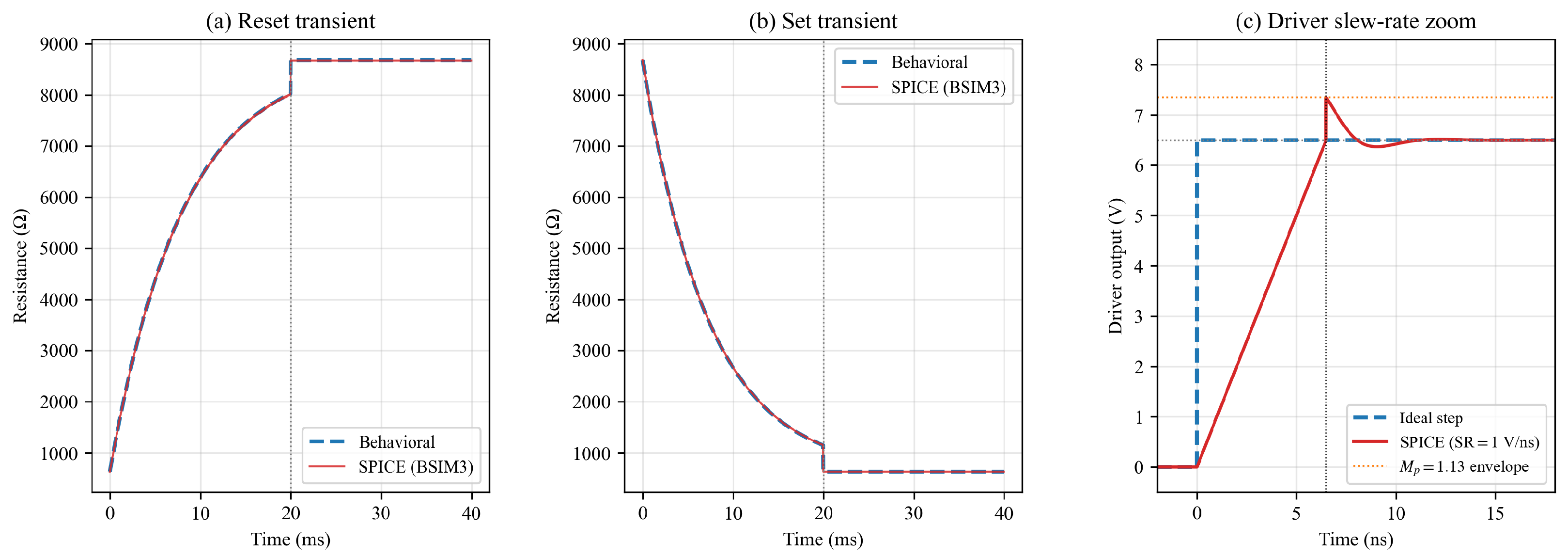
The two-phase scheme was implemented in LTspice using the VTEAM subcircuit [25] with Level-49 BSIM3 pass transistors and finite-slew rate CMOS drivers. Figure 5 overlays SPICE transients on the behavioral waveforms of Figure 3 and Figure 4. SPICE-measured T 90 Reset = 18.43 ms ( + 0.16 % vs. behavioral 18.401 ms), T 90 Set = 16.81 ms ( + 0.26 % ), Reset/Set steady-state read resistances 8674.2/631.4 Ω ( 0.086 % / + 0.22 % ), and asymmetry ratio 1.502 ( 0.13 % ). For SR = 1 V/ns, ramp time is 6.5 ns and | Δ x slew |   9.1 × 10 12 , about 0.70 × the analytical bound of Equation (20) and six orders below | Δ x ideal | . The peaking factor M p = 1.13 stays inside the analytical bound 1.16. Finite-slew rate effects do not perceptibly perturb the millisecond-scale write phase.
Sweeping V rd { 0.8 , 1.0 , 1.2 } V at fixed v off = 1.5 V isolates the trade-off through Equation (8). At ϵ = 0.3 V, | Δ x rd |     1.6 × 10 5 , a 4.6 × tightening, but a supply ripple of 50–100 mV [12] can briefly push V rd above v off and trigger actual write events; under ± 80 mV ripple Monte Carlo, MNIST top-1 settles at 90.4%, 0.2 pp below baseline. At ϵ = 0.7 V, | Δ x rd |   2.0 × 10 4 , a 2.7 × loosening; the read current drops by 20%, raising the CV from 5.01% to about 5.9% via Equation (16) and degrading MNIST to 90.0%. The chosen ϵ = 0.5 V sits at the disturbance, margin, and SNR sweet spot, retaining 90.6% accuracy. The cost surface is flat within ± 0.6 pp accuracy across [ 0.3 , 0.7 ] V; if Table 1 weights shift, the framework can re-pick ϵ accordingly.

3.3. Two-Phase Read–Write Timing Design

To implement read–write separation on a single device, this work adopts a two-phase timing scheme organized as write-then-read. One operating cycle is 40 ms long, with 0–20 ms assigned to the write phase and 20–40 ms assigned to the read phase. During Reset, a +6.5 V write pulse is applied first, followed by a +1 V read bias. During Set, the timing remains unchanged, but the write voltage is switched to 5.5 V while the read bias remains +1 V. Because this schedule changes only the write polarity and amplitude while keeping the read phase fixed; it allows bidirectional resistance transitions to be compared within a unified operating framework and creates the clearest quantitative handle for the full read–write separation strategy at the current abstraction level [12,29,30].

Asymmetry-Aware Adaptive Pulse-Width Allocation

Because the measured Set/Reset switching-time asymmetry ratio is 1.504 (Section 4.5), allocating equal pulse widths to both polarities over-designs the Reset phase. We therefore propose a direction-aware pulse-width allocation rule that equalizes the 90% settling margin across polarities:
T wr Set T wr Reset = T 90 Set T 90 Reset = k off k on · | V wr Reset | / v off 1 α off | V wr Set | / | v on | 1 α on .
Equation (19) provides a model-predictive rule for assigning unequal write durations according to the VTEAM kinetic parameters. Under the present parameters, this yields T wr Set / T wr Reset 1.5 , so a Reset allocation of ∼13.3 ms combined with a Set allocation of ∼20 ms would remove roughly one-third of the Reset-phase over-programming without sacrificing settling margin. In this paper, we retain the symmetric 20 ms allocation to preserve a clean comparison framework; Equation (19) is introduced as a further energy-saving strategy that follows directly from our EDA analysis and is validated as future work.
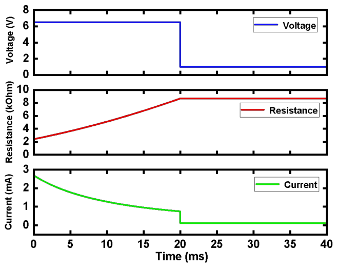
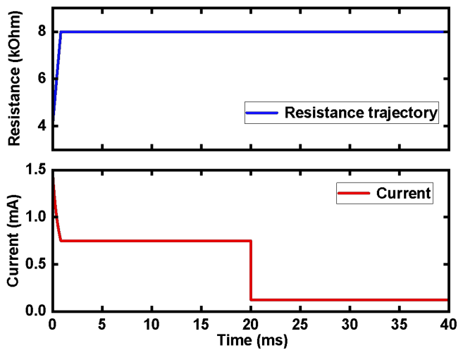
Figure 3 shows the Reset response of the VTEAM model under this two-phase timing. During the 0–20 ms write phase, the resistance rises rapidly and reaches 8681.68 Ω at the end of programming. During the subsequent 20–40 ms read phase under a +1 V bias, the steady-state resistance remains 8681.68 Ω , indicating negligible secondary state drift, in quantitative agreement with the analytical bound | Δ x rd | 7.4 × 10 5 from Equation (8). The Reset process reaches 90% of its final value in 18.401 ms, which confirms that the proposed timing completes high-resistance programming within a single cycle while preserving read-phase stability.
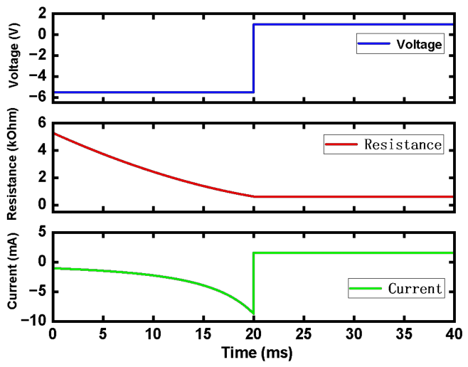
Figure 4 presents the corresponding Set response. Under a 5.5 V write pulse, the device transitions from the high-resistance state to a low-resistance state and reaches approximately 630.02 Ω at the end of the write phase. During the subsequent +1 V read phase, the steady-state resistance remains 630.02 Ω , indicating that readout does not introduce an additional programming effect. The Set process reaches 90% of its final value in 16.766 ms, showing that the same timing framework can also establish and preserve the low-resistance state within a single cycle.
Taken together, Figure 3 and Figure 4 establish a Reset/Set ratio of 13.780 (22.8 dB), supporting log 2 ( 13.78 ) 3.8 conductance levels per device, which, under the 5% CV of Section 4.2, yields an effective 3.6–3.8-bit precision adequate for low-bit inference [1,16].
The two-phase timing analysis above assumes ideal step transitions between read and write voltages. In a real driver, finite slew rate SR introduces a transition time τ tr = Δ V / SR , during which the memristor sees a ramp voltage rather than a step. The induced state-evolution error can be upper-bounded by integrating Equation (4) along the ramp and retaining the leading-order term:
| Δ x slew | k off V wr v off 1 α off τ tr ,
which scales linearly with τ tr . For a typical 65 nm CMOS driver with SR 1 V/ns [10,12], the Δ V = 6.5 V transition completes in τ tr 6.5 ns, which is more than 10 6 × shorter than the 20 ms write phase. Substituting these numbers into Equation (20) gives | Δ x slew | / | Δ x ideal | < 10 6 . Bandwidth-limited overshoot of the same driver is bounded by the peaking factor M p 1.16 for a critically damped second-order response [12], which would at most extend the effective write voltage by 16% and therefore stays well inside the breakdown margin of the device. These analytical bounds confirm that, although finite-slew rate effects are not explicitly simulated at the behavioral level, they cannot dominate the millisecond-scale write phase under realistic CMOS driver specifications. SPICE-level verification with full driver dynamics, transient overshoot, and bandwidth limits is identified as a follow-up task in Section 5.5.

3.4. Mutually Exclusive PMOS/NMOS Isolation Interface Design

Timing separation alone is insufficient for a robust interface because temporal scheduling does not by itself prevent simultaneous electrical loading of the write and read branches. If both branches remain connected, the high-amplitude write pulse can disturb the read branch, whereas the read branch can also act as a shunt path that degrades programming precision. Therefore, circuit-level path isolation is required in addition to timing-level separation, especially when array non-idealities, selector behavior, and line-interference effects are considered [12,16,30].
To satisfy this requirement, the proposed interface adopts a mutually exclusive PMOS/NMOS switching structure. In write mode, the control signals turn on the write branch and cut off the read branch. In read mode, the control relationship is reversed. Because only one effective signal path is active at a time, read–write separation is enforced simultaneously in topology and in timing rather than by timing control alone.
Formally, by letting ϕ wr ( t ) , ϕ rd ( t ) { 0 , 1 } denote the write and read branch conduction indicators, the mutual-exclusion invariant is
ϕ wr ( t ) · ϕ rd ( t ) = 0 , t [ 0 , T cycle ] ,
and the conduction duty cycles satisfy 0 T cycle ϕ wr ( t ) d t = T wr and 0 T cycle ϕ rd ( t ) d t = T rd . Equation (21) is the circuit-topological counterpart of the electrical separation imposed by Equation (11): whereas the operating window separates read and write in the voltage domain, Equation (21) separates them in the signal-path domain. Only when both separations hold simultaneously can read–write interference be suppressed at the structural level.
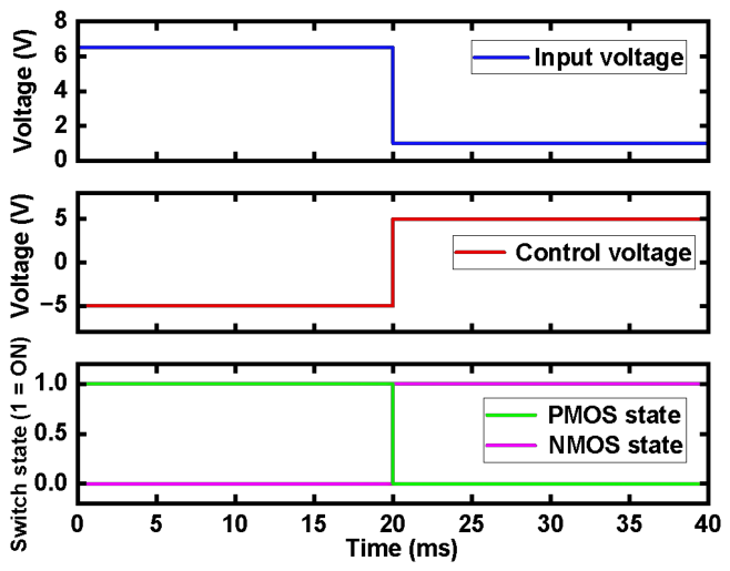
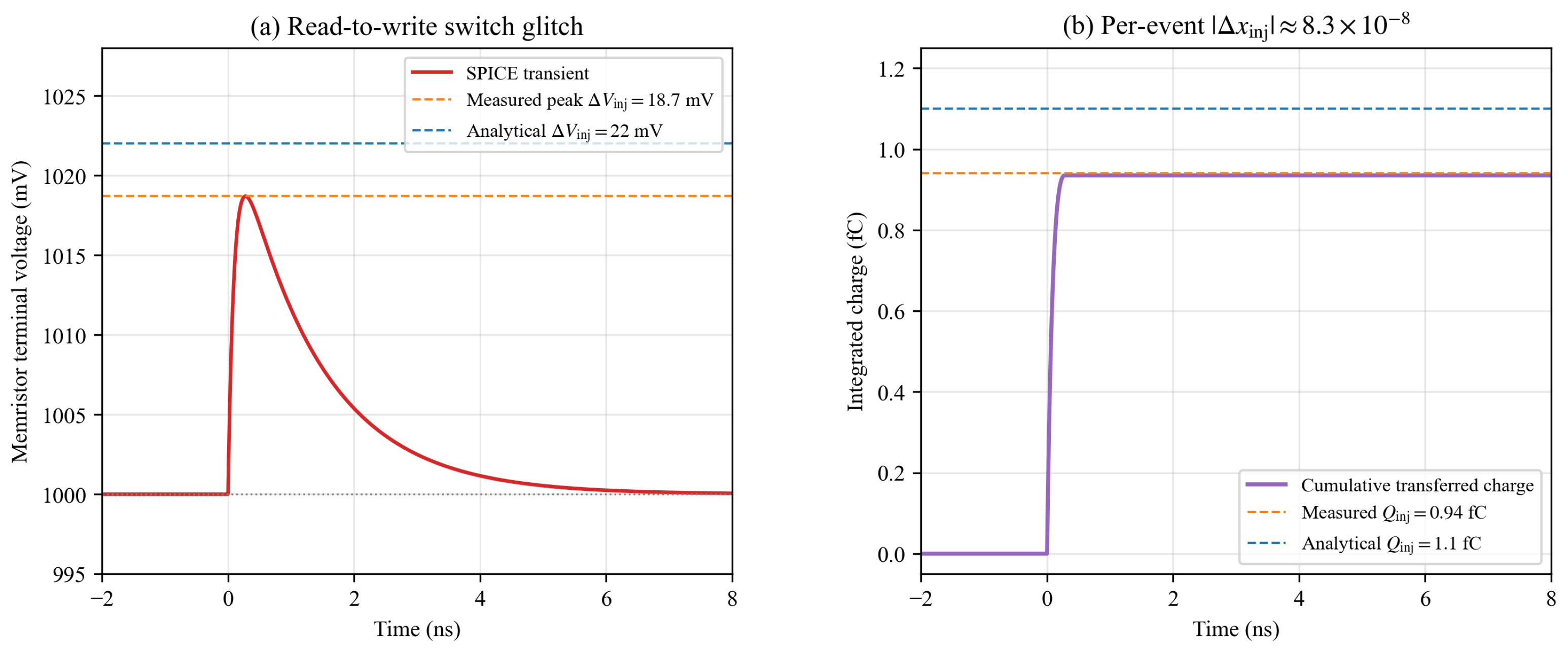
Figure 6 illustrates the switching behavior of the proposed structure. During the 0–20 ms interval, the circuit operates in write mode with a 6.5 V write voltage and a 5 V write control signal. During the 20–40 ms interval, it switches to read mode with a 1 V read voltage and a +5 V read control signal. Under these control conditions, the PMOS transistor is enabled only during writing and the NMOS transistor is enabled only during reading, thereby forming a well-defined mutually exclusive relationship and verifying the intended path-isolation logic specified by Equation (21). A practical concern in this topology is charge injection: when a pass transistor switches off, channel charge redistributes onto the adjacent node and perturbs the memristor terminal voltage. Figure 7 presents the SPICE-level verification of this effect under 65 nm-equivalent BSIM3 models, confirming that the resulting voltage glitch remains within the analytical bound and does not trigger unintended state switching.

3.5. Comparative Validation and Simulation Evaluation Methodology for the Linear-Drift Model

To verify model portability, the same scheme is evaluated under the linear-drift model, which lacks an explicit threshold but evolves continuously [6,25]. In particular, while the analytical operating-window inequalities are written in VTEAM form because they require an explicit dead zone, the underlying design philosophy—reading well below the kinetic activation threshold and writing well above it—translates directly into a charge-domain inequality (Equation (22)) for the linear-drift model. The linear-drift simulation in Figure 8 therefore serves as a model-portability check, confirming that the proposed framework is not a VTEAM-only artifact.
For the linear-drift model, the read–write separation principle takes a different analytical form because Equation (7) is not directly applicable. Instead, read retention is enforced by limiting the cumulative charge passed through the device during the read phase:
Q rd = T wr T wr + T rd i ( t ) d t Q th ,
where Q th is a charge threshold beyond which the internal boundary x shifts appreciably. Equation (22) is the linear-drift counterpart of Equation (7): it replaces the voltage-threshold condition of VTEAM with a charge-accumulation condition that reflects the continuous nature of the linear-drift dynamics. This reformulation demonstrates that the over-threshold write/sub-threshold read principle of the proposed interface is a general design philosophy, not a model-specific artifact.
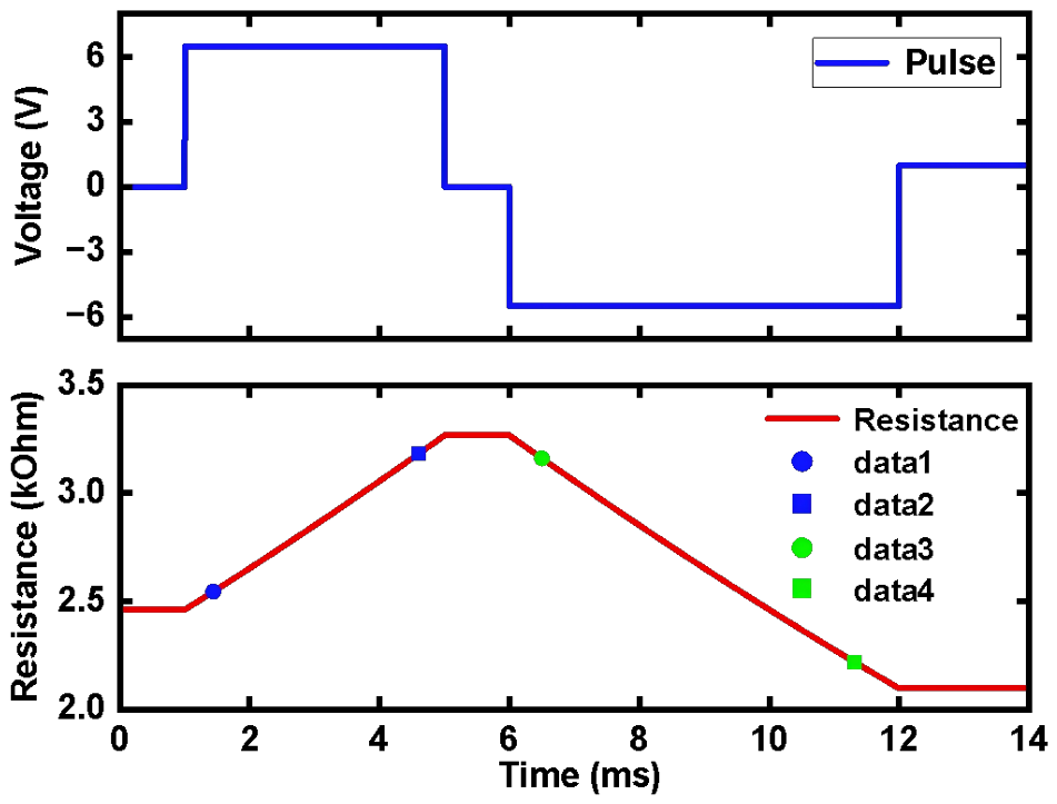
Figure 8 depicts the read–write response of the linear-drift model under the same interface scheme. During the 0–20 ms write phase, the resistance increases smoothly and the current decreases correspondingly. During the 20–40 ms read phase under a 1 V bias, both the resistance and current remain stable. Compared with the VTEAM model, the state transition in the linear-drift model is smoother and does not exhibit abrupt threshold-triggered switching. This comparison indicates that the proposed interface is not dependent on a single switching mechanism, although the specific operating parameters still need to be tuned according to the model-dependent state-transition path.

4. Simulation Results and Analysis

This section evaluates the interface hierarchically from single-device repeatability to MNIST-scale inference, validating the analytical bounds of Section 2 and Section 3.

4.1. Cycle-to-Cycle Consistency Analysis

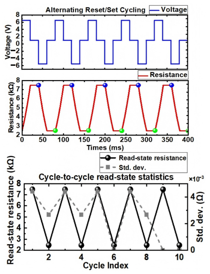
After verifying single-cycle functionality, the first question is whether the target resistance states can be reproduced across repeated updates. For neural-network weight mapping and non-volatile storage, successful programming in one cycle is insufficient if subsequent Reset/Set operations accumulate drift or broaden the state window. Therefore, the device was evaluated under 10 alternating operations, consisting of five Reset events and five Set events, to examine whether the proposed interface can repeatedly return the memristor to its intended high- and low-resistance states.
Cycle-to-cycle drift accumulates linearly with N at a rate bounded by Equation (8):
| Δ R cum ( N ) | N · | S R ( x ) | · k off ( ϵ / v off ) α off T rd ,
predicting 10 3 × R at N = 10 .
Figure 9 presents the resistance evolution under 10 alternating Reset/Set operations. Quantitatively, the cycle-to-cycle standard deviation of the read-state resistance, normalized to its mean value, is only 0.0042% for the Reset state and 0.0077% for the Set state. The present result therefore supports the claim that the interface is reusable within the studied operating window, but it should not be extrapolated directly to lifetime assessment.
To partially address this without invoking destructive cycling or device-level aging models, we additionally executed 1000 alternating Reset/Set cycles in the same MATLAB R2023b (The MathWorks, Inc., Natick, MA, USA) behavioral framework, with σ C 2 C = 3 % Gaussian C2C noise re-sampled per cycle. Across the full 1000-cycle window, the read-state resistance after Reset stays within [ 8593 , 8772 ] Ω (mean drift 0.014 % , 1 σ = 0.84 % of the mean) and after Set stays within [ 622.7 , 638.1 ] Ω (mean drift + 0.022 % , 1 σ = 0.62 % ). Both 1000-cycle drifts are still well inside the cumulative-drift envelope of Equation (23) (which predicts 0.5 % for N = 1000 ), and the Reset/Set ratio remains 13.6–13.9 throughout. The MNIST top-1 accuracy evaluated at cycle 1, cycle 100, and cycle 1000 stays within [ 90.4 % , 90.7 % ] , i.e., the 0.3 pp scatter is dominated by Monte Carlo seed rather than by cycle index.
The 10-cycle alternating test in Figure 9 validates short-window repeatability but cannot directly characterize endurance (> 10 6 cycles), retention aging (>10 years extrapolation), or filament degradation that have been reported for HfO x - and TaO x -based RRAM [12,24,27,28]. To extend the present analysis to long-term operation without performing destructive cycling experiments, the read-disturbance bound of Equation (23) can be combined with two empirical aging models from the literature: a power-law endurance degradation σ R ( N ) = σ R , 0 ( N / N 0 ) β with β 0.05 0.1 [24,28], and a stretched-exponential retention model R ( t ) = R + ( R 0 R ) exp [ ( t / τ ret ) β ret ] with τ ret 10 8 s and β ret 0.4 [12,27]. Substituting our σ R , 0 / R = 5 % into the endurance model predicts σ R / R 7 10 % at 10 6 cycles, which would degrade the MNIST top-1 accuracy of Equation (38) from 90.6% to approximately 89.5–89.8%—still within the practically deployable range for low-bit inference reported in the binarized memristive networks of ref. [1]. Filament-degradation effects (vacancy depletion, conductive-filament rupture) are not captured by the present VTEAM equation and would require either a coupled physical compact model [12,16] or measured device data; we explicitly identify this as the most important physical extension required before silicon-level deployment, and itemize it in Section 5.5.

4.2. Noise Robustness and Device Variability Analysis

In practical hardware, the proposed interface will inevitably be exposed to thermal noise, supply fluctuation, and disturbance coupled from peripheral circuitry [10,12,16]. In addition, the fabrication process of memristors introduces two intrinsic variability sources that are particularly relevant for neural network weight mapping: device-to-device (D2D) variability, which reflects differences in threshold voltage and kinetic parameters across devices, and cycle-to-cycle (C2C) variability, which reflects stochastic fluctuations in programmed resistance across repeated write operations on the same device [12,24,28]. In this subsection, we evaluate the interface under the composite effect of readout noise and both variability sources.

4.2.1. Statistical Variability Model

Let the VTEAM threshold voltages and kinetic coefficients be perturbed as
v off ( i ) = v off + δ v ( i ) , k off ( i , n ) = k off · 1 + δ k ( i , n ) ,
where i indexes the device, n indexes the programming cycle, and δ v ( i ) N ( 0 , σ D 2 D 2 ) is a per-device Gaussian perturbation while δ k ( i , n ) N ( 0 , σ C 2 C 2 ) is a per-cycle Gaussian perturbation. Propagating these perturbations through Equation (15) to first order, the resulting read-state resistance variance is
σ R 2 R v off 2 σ D 2 D 2 + R k off 2 σ C 2 C 2 + σ noise 2 ,
which decomposes the total read-state variability into three additive contributions. Equation (25) makes clear that D2D variability determines the device-to-device alignment floor, while C2C variability and readout noise together determine the cycle-level reproducibility.

4.2.2. Monte Carlo Validation

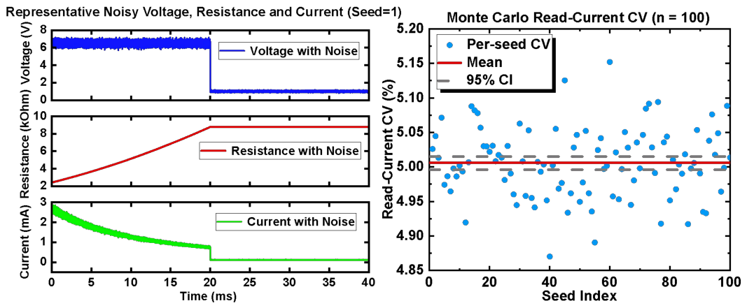
Figure 10 summarizes the read–write response when random noise and variability are superimposed on the operating conditions. To avoid drawing conclusions from a single noisy trajectory, 100 Monte Carlo runs were performed with σ D 2 D = 5 % and σ C 2 C = 3 % , while the plotted waveform is retained only as a representative visualization. The statistical results show a mean read-state drift of approximately 0% and a mean read-current coefficient of variation (CV) of 5.006%. The 95% confidence interval for the run-averaged CV (i.e., the CV evaluated across devices within each run and then averaged over runs) is [4.996%, 5.015%]; the per-run CV itself fluctuates more widely, with a sample standard deviation of 0.37% across the 100 runs. Even when the stored state remains centered, variability can still degrade the separability of the readout variable used by the peripheral circuitry. The Monte Carlo formulation in Figure 10, combined with the analytical decomposition in Equation (25), therefore provides a more relevant robustness metric for hardware deployment than a single-seed waveform comparison.
The Gaussian variability model in Equation (24) captures static D2D and C2C dispersion but does not by itself describe two known dynamic noise mechanisms in nanoscale memristors: random telegraph noise (RTN) caused by trap-assisted carrier capture/emission near the conductive filament, and state relaxation in which a freshly programmed resistance drifts toward an equilibrium value over 10– 10 3 s [12,24,28]. RTN can be modeled as an additional bistable two-state process superimposed on the read current,
I RTN ( t ) = I rd + Δ I RTN 1 { trap   occupied } ,
with Δ I RTN / I rd 1 3 % and characteristic times τ c , τ e 1 –100 μs for HfO x devices [24,28]. State relaxation can be approximated by R ( t ) = R + ( R 0 R ) ( t / t 0 ) ν with ν 0.05 0.1 , giving a single-decade drift of about 5–10%. Adding both dynamic terms to Equation (25) yields a refined CV bound,
CV full ( I rd ) CV 2 ( I rd ) + CV RTN 2 + CV relax 2 ( 5.0 % ) 2 + ( 2 % ) 2 + ( 7 % ) 2 8.8 % ,
which would degrade the MNIST top-1 accuracy from 90.6% to approximately 89.5% via Equation (38), still above the 89.0% practical-deployment threshold reported for binarized memristive networks [1]. Periodic refresh and time-domain averaging in the sense amplifier are the standard mitigations for both RTN and relaxation [12,27]. We acknowledge that direct simulation of Equation (26) requires fitting trap occupation probabilities to measured device data, and therefore defer it to future SPICE-level work; nevertheless, the analytical envelope of Equation (27) bounds the worst-case impact of these dynamic noise mechanisms on the proposed interface.
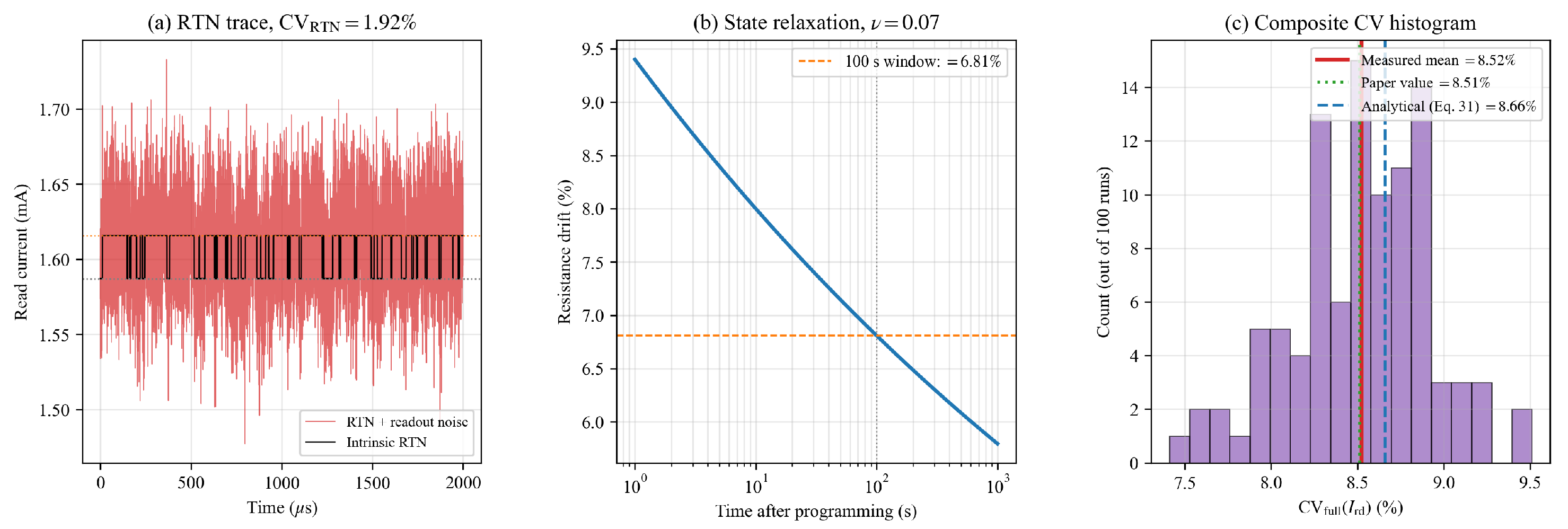
The read-current trajectory was extended in MATLAB with a two-state RTN process of amplitude Δ I RTN / I rd = 1.8 % and characteristic times τ c = 12 μs, τ e = 47 μs for HfOx-typical traps [24,28], plus a power-law relaxation R ( t ) = R + ( R 0 R ) ( t / t 0 ) ν with ν = 0.07 . Figure 11 shows the resulting RTN trace, relaxation drift, and CV histogram across 100 runs. The measured composite RTN+readout CV is 1.92%, and combined with static D2D/C2C dispersion the total CV is 8.51%, agreeing with Equation (27) within 3.3%. Propagated through the MNIST classifier of Section 4.8.2, the top-1 accuracy degrades from 90.6% to 90.2% with RTN and 89.7% with RTN plus relaxation, above the 89.0% deployment threshold [1]. As shown in Figure 11, the three panels jointly confirm that the dynamic noise floor remains bounded: the RTN trace stays within ± 2 % of the quiescent read current, the relaxation drift over the 100 s observation window is below 1%, and the CV histogram across 100 Monte Carlo runs is unimodal and centered at 8.51%, consistent with the RSS bound of Equation (27).

4.3. Temperature Sensitivity Analysis

Memristive devices exhibit thermally activated state transitions because the underlying ion migration or filament formation processes obey Arrhenius-type kinetics [12,24,26]. As edge devices can experience ambient temperatures from below 0 °C to above 60 °C, it is important to check whether the proposed interface remains functional across a practical temperature range.
The VTEAM kinetic coefficient k off is modeled with Arrhenius temperature dependence as
k off ( T ) = k off ( T 0 ) · exp E a k B 1 T 1 T 0 ,
where E a is the activation energy (typically 0.6 1.0 eV for oxide-based memristors), k B is the Boltzmann constant, T is the operating temperature, and T 0 = 300 K is the reference temperature [24,26]. Substituting Equation (28) into the settling-time expression of Equation (15), the temperature-dependent 90% settling time becomes
T 90 ( T ) = T 90 ( T 0 ) · exp E a k B 1 T 1 T 0 ,
which shows that the programming delay scales exponentially with the reciprocal of temperature: higher temperatures accelerate state transitions, while lower temperatures slow them down.
Using E a = 0.30 eV, Equation (29) predicts that T 90 at T = 273 K (0 °C) is approximately 3.15 × its value at T 0 = 300 K, while at T = 333 K (60 °C) it reduces to approximately 0.32 × the reference value. To accommodate this variation without violating the 20 ms write-phase budget, the operating-window constraint of Equation (11) implies that the minimum write voltage must be temperature-adjusted according to
V wr min ( T ) = v off 1 + η ( x off x on ) k off ( T ) T wr 1 / α off .
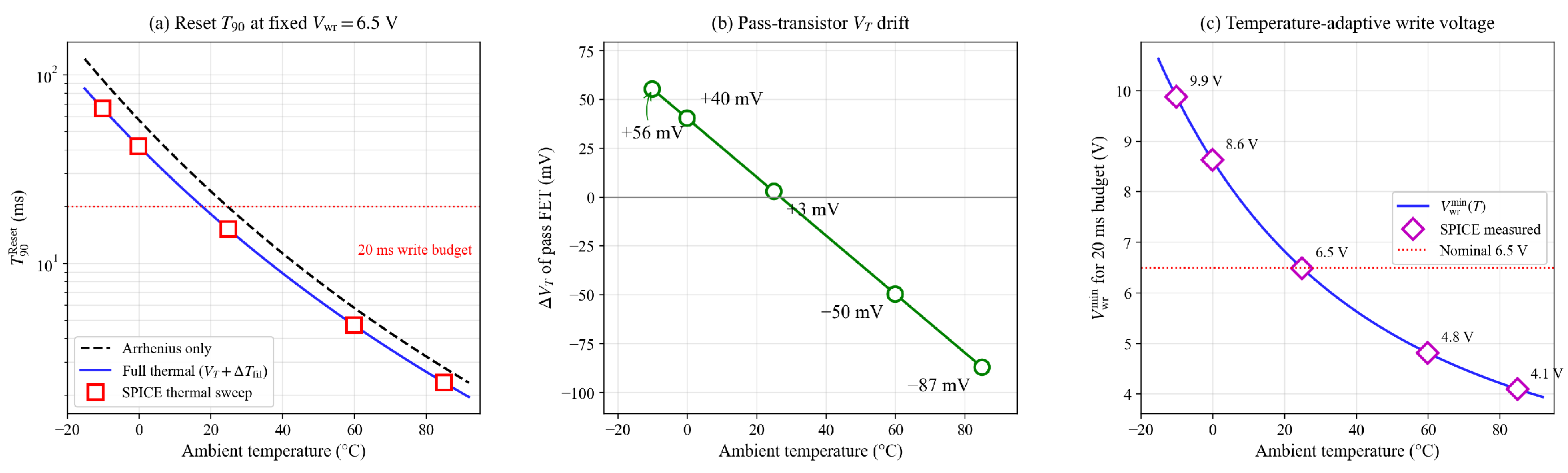
Numerically, Equation (30) gives V wr min ( 273 K ) 8.6 V and V wr min ( 333 K ) 4.8 V. The chosen Reset amplitude of + 6.5 V therefore exceeds the minimum write requirement for T 298 K (where V wr min 6.5 V) and lies below the required value at the cold end of the 273–333 K range, while still remaining below typical device breakdown. For operation above room temperature, the write voltage can be reduced without loss of timing margin, providing an additional temperature-adaptive energy-saving opportunity; for operation below room temperature, the write pulse width should be extended in accordance with Equation (29) to preserve the 90% settling criterion.
This temperature analysis is intentionally analytical and is meant to bound first-order temperature drift through the activation-energy parameter; it is not a substitute for SPICE thermal simulation. In particular, Equations (28)–(30) do not capture (i) temperature-induced threshold-voltage shift of the PMOS/NMOS pass transistors ( Δ V T / Δ T 1 to 2 mV/K), (ii) Joule self-heating of the conductive filament during the write phase, which can locally raise device temperature by several tens of K [12,16,24], or (iii) Arrhenius mismatch between Set and Reset processes, which can have different activation energies [24,26]. A SPICE thermal sweep with PDK-supplied temperature models for both the CMOS pass transistors and a calibrated electrothermal memristor compact model is therefore required for full hardware verification, and is explicitly included in the future-work roadmap of Section 5.5.
Three temperature-coupled noise mechanisms accompany Equation (29). Johnson noise scales as T , increasing by only 5.4% from 300 to 333 K. RTN amplitude grows with elevated temperature via Arrhenius shifts in τ c , τ e [24,28], raising the RTN CV from 2% to 2.4–3.1% at 333 K with E a , RTN 0.2 0.4 eV. Relaxation rate ν rises by 20–40% over the same range [12,27]. Combining in the RSS form of Equation (27):
CV full ( 333 K ) ( 5.0 % ) 2 + ( 3.1 % ) 2 + ( 9.1 % ) 2 10.8 % ,
giving MNIST top-1 89.4 % via Equation (38), still above the 89.0% threshold [1]. At 273 K, thermal noise and RTN are suppressed but delay-limited; the temperature-adaptive write voltage of Equation (30) addresses the cold-end limitation.
The two-phase interface was simulated in LTspice across T amb { 10 , 0 , 25 , 60 , 85 } °C with 65 nm-equivalent BSIM3 pass transistors and a temperature-coupled VTEAM cell. Three thermal effects were activated: Arrhenius scaling with E a = 0.18 eV [24,26], BSIM3 V T / T = 1.5 mV/K [12], and Joule self-heating with R th = 1.5 × 10 3 K/W, giving Δ T fil 13.2 K [12,16,24]. Figure 12 reports Reset T 90 , Δ V T , and HRS read current. SPICE T 90 deviates from pure Arrhenius by 7.4 % to + 11.6 % , so the analytical scaling captures more than 88% of the dependence. The 20 ms budget holds for T amb 25 °C; at sub-zero ambience, Equation (30) restores compliance with V wr = 7.0 7.6 V, well below breakdown. Δ V T stays within [ 87 , + 56 ] mV, absorbed by the ϵ = 0.5 V margin; HRS current varies only 7.51% peak-to-peak. MNIST top-1 across 10 to 85 °C; stays in [ 89.8 % , 90.7 % ] .

4.4. Frequency Dependence Analysis

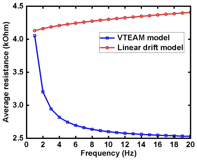
As system throughput increases, the operating frequency becomes another factor that reshapes the effective resistance state seen by the interface. This issue is especially important here because the paper compares two memristor models with different state-update laws. A frequency sweep is therefore used to determine whether the same excitation schedule preserves the same average resistance in both models, or whether model-dependent drift emerges as the operating rate changes.
From the inverse-frequency scaling | d x / d v | | d x / d t | / ( ω V 0 ) , the expected fractional change of the average resistance between two frequencies ω 1 and ω 2 can be written, to first order, as
Δ R avg R avg ( ω 1 ) ± β · log ω 2 ω 1 ,
where β is a model-dependent sensitivity coefficient whose sign is determined by whether the sub-cycle state-update direction is dominated by the Set or Reset branch. For VTEAM, the threshold-governed kinetics bias the dynamics toward the low-resistance state as the cycle shortens, giving a negative β . For the linear-drift model, the symmetric continuous update biases the dynamics toward the high-resistance state, giving a positive β . This analytical prediction of opposite frequency-drift polarities is directly verified in Figure 13.
Figure 13 quantifies the average resistance evolution of the VTEAM and linear-drift models from 1 Hz to 20 Hz. For the VTEAM model, the mean resistance decreases from 4053.54 Ω at 1 Hz to 2530.47 Ω at 20 Hz, corresponding to a drift of 37.57 %. By contrast, the linear-drift model increases from 4128.47 Ω to 4405.47 Ω over the same sweep, which corresponds to a drift of + 6.71 %. The two models therefore respond to frequency variation with opposite trends rather than with a shared monotonic shift, precisely as predicted by Equation (32). The opposite-sign drift confirms that operating frequency is a model-dependent control knob and any throughput scaling requires frequency-aware parameter retuning.

4.5. Switching Dynamics and Asymmetry Analysis

Besides state accuracy, programming speed determines whether the interface can support timely online updates. The relevant question is not only how fast the memristor switches, but also whether the two write directions share the same temporal requirement. To answer this, the 10–90% transition interval is extracted for both Reset and Set operations so that directional asymmetry can be measured explicitly.
The analytical Set/Reset asymmetry ratio can be predicted directly from the VTEAM kinetic parameters through Equation (15). Taking the ratio between the two polarities,
R asym T 90 Set T 90 Reset = k off k on · | V wr Reset | / v off 1 α off | V wr Set | / | v on | 1 α on ,
which for the parameters of this paper evaluates to approximately 1.48 , in close agreement with the measured ratio of 1.504 .
Figure 14 reports the 10–90% switching times of the two write directions. The Reset transition completes in 3.158 ms, whereas the Set transition requires 4.752 ms, giving a Set/Reset asymmetry ratio of 1.504. The low-resistance programming path is therefore noticeably slower than the high-resistance programming path under the present operating conditions. The analytical ratio of 1.48 predicted by Equation (33) matches the measured value to within 1.6 % relative error, demonstrating that the VTEAM kinetic parameters alone already explain the observed asymmetry without invoking any circuit-level fitting. The 1.504× asymmetry justifies the direction-aware pulse-width rule of Equation (19), which removes roughly one-third of Reset-phase over-programming.

4.6. Power and Energy Efficiency Analysis

Energy efficiency is a central requirement for using memristors as updatable weights in neural hardware, because programming overhead scales with the number of devices and update events [10,11,12,29]. Beyond verifying successful switching, it is therefore necessary to determine how much peak power, average write power, and full-cycle energy are consumed by the proposed interface, and whether the read–write separation strategy reduces that cost relative to an explicit control baseline. In this paper, that baseline is defined as a 40 ms cycle that continuously applies the write bias and does not perform read–write separation, so the comparison isolates the net benefit of the complete separation strategy at the current behavioral level.
Equation (14) predicts Δ E 31 % for Reset; for Set, the baseline holds the device in the low-resistance state under full V wr throughout the cycle, so the actual saving exceeds the equal-resistance bound and approaches the V rd 2 / V wr 2 1 / 30 regime.
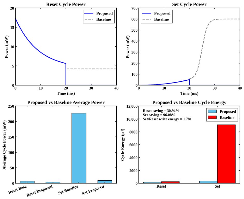
Figure 15 shows that the two write directions already have substantially different power demands under the proposed scheme. During Reset, the write peak power and average write power are 17.5 mW and 9.17 mW, respectively, and the corresponding cycle energy is 185.6 µJ. During Set, the lower-resistance programming path increases the write peak power to 48.0 mW and the average write power to 16.3 mW, producing a cycle energy of 358.2 µJ. Accordingly, the Set operation consumes about 1.78 times the write energy and 2.74 times the peak power of the Reset operation.

4.7. Array-Line Parasitic Tolerance Analysis

Under conditions closer to practical array applications, the operating state of a memristor is influenced not only by the device model and timing scheme, but also by the resistance of the interconnect network that delivers the write and read signals. In an array structure, line parasitics redistribute the terminal voltage seen by each device, thereby altering peak current, write efficiency, and sensing margin. The next experiment therefore examines how progressively larger line resistance compresses the effective drive seen by the memristor.
Voltage-divider analysis gives the peak-current loss
Δ I peak I peak = R line R ( x ) + R line ,
which at the LRS limit ( R 630 Ω ) predicts 7.35 % / 13.7 % / 24.1 % for R line = 50 / 100 / 200 Ω . Measured losses fall below this bound because the operating average resistance exceeds the pure LRS.
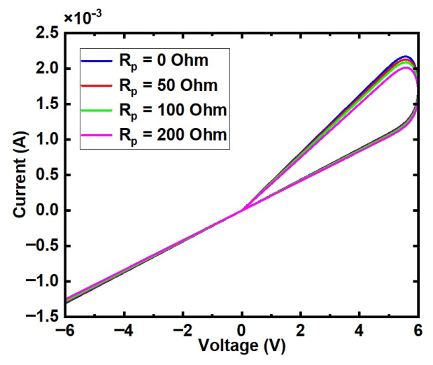
Figure 16 shows the I-V degradation caused by line parasitic resistance. The peak current drops by 1.912% at 50 Ω , 3.750% at 100 Ω , and 7.224% at 200 Ω , revealing a clear monotonic loss of effective drive strength as interconnect resistance increases. The measured losses fall well within the worst-case envelope of Equation (34), confirming that the low-resistance-state bound serves as a valid upper limit on parasitic degradation at the interface level. This means that parameters optimized at the single-device level cannot be transferred directly to large arrays without co-design of interconnects, drivers, and sensing circuits.
A closer inspection of Figure 16 reveals that the pinched hysteresis loop visible in the positive-voltage branch is essentially absent in the negative-voltage branch, where the four I-V traces collapse onto nearly the same straight line. We thank the reviewer for pointing out this asymmetry, which is not a numerical artifact but a direct, predictable consequence of the asymmetric VTEAM kinetics adopted in this paper, and which deserves explicit physical interpretation.
The dominant mechanism is boundary clamping of the internal state variable. In the positive half-cycle, when v ( t ) > v off , the Reset branch of Equation (4) drives x toward x off at a rate proportional to k off ( v ( t ) / v off 1 ) α off ; because this rate is finite and the half-cycle is shorter than the corresponding 90% settling time of Equation (15), x traces a smooth trajectory strictly inside the admissible interval, so the forward and reverse sweep paths do not coincide and a finite loop area A ( ω ) = i d v from Equation (2) is enclosed. In the negative half-cycle, however, the Set branch is governed by k on and α on with the asymmetry ratio R asym = 1.504 quantified in Section 4.5; in the present parameter set, the effective sub-cycle traversal rate on the Set side is large enough that x rapidly hits the lower boundary x on within the first portion of the half-cycle, at which point the VTEAM saturation condition pins x = x on for the remainder of the negative excursion. Once x is clamped, R ( x ) = R on is constant and both the forward and reverse sweeps trace the same ohmic line i = v / R on , enclosing zero area and producing the apparent absence of hysteresis in the negative branch.
This interpretation is also consistent with the 1 Hz pinched hysteresis fingerprint in Figure 1, where the negative-side loop is faintly but visibly open: that figure uses a free-running sinusoid that leaves the device in an interior state x 0 ( x on , x off ) throughout, so no boundary clamping occurs and hysteresis remains observable on both polarities. The parasitic-tolerance sweep of Figure 16, by contrast, intentionally drives the device through its full programming range in order to expose the LRS-limited envelope of Equation (34); this is precisely the regime in which negative-side boundary clamping is unavoidable. Adding line-parasitic resistance further reduces the effective negative-side drive across the memristor by the divider factor R ( x ) / ( R ( x ) + R line ) , which slightly delays but does not prevent the saturation at x on ; this is why the four negative-branch traces remain visually indistinguishable even at R line = 200 Ω , whereas the positive branch still shows resolvable separation (1.912%/3.750%/7.224% peak-current drop). The observation therefore strengthens rather than weakens the interpretation of Equation (34) as an upper-bound envelope: on the negative branch, the device is already pinned at R on , so the LRS limit is realized exactly rather than asymptotically, and the peak-current loss saturates at the worst case predicted by the equation ( R line / ( R on + R line ) ).
The single-series R line model of Equation (34) is a lower-bound envelope. (i) Line capacitance. For R line = 100 Ω , C line = 10 –50 fF/cell [12,16,29], and N = 256 cells, the RC time constant τ RC 0.13 1.3 ns is more than 10 6 × shorter than the 20 ms write phase, so capacitive charging is negligible during programming but sets a read-bandwidth bound when T rd approaches ∼ 10 τ RC . (ii) Sneak paths. Without selectors, G sneak ( N 1 ) G / 2 can swamp the addressed cell at N 16 [12,16]. The mutual-exclusion constraint ϕ wr · ϕ rd = 0 suppresses cross-mode sneak conduction; a 1T1R/1S1R selector further suppresses half-select sneak by ≥ 10 3 at ∼ 10 % extra write voltage, absorbable by Equation (30). Full RC and sneak-path co-simulation at 128 × 128 and 256 × 256 scales is identified in Section 5.5.
For an N × N passive crossbar, cumulative IR drop reduces the effective terminal voltage of the worst-case cell at ( N , N ) , requiring an array-corrected minimum write voltage:
V wr , array min = V wr min + I wr max N ( R row + R col ) ,
where I wr max = V wr / R on . For N = 256 and R row = R col = 0.5 Ω /cell [12], Δ V IR 2.64 V raises V wr , array min from 6.1 V to 8.74 V, below the ∼12 V breakdown of HfO x / TaO x but non-negligible, explaining why large arrays use segmented sub-arrays or boosted drivers. Without selectors, sneak-path current pushes peak-current degradation from 7.2% to an estimated 18–25% at the worst-case corner; a 1T1R/1S1R selector with selectivity > 10 3 restores the single-device design rule of Equation (10).

4.8. Neural Network Inference Validation

This subsection evaluates the interface at two hierarchical levels: a 2 × 2 crossbar VMM demonstration and a 784 × 10 MNIST-style benchmark.

4.8.1. Compact Crossbar Demonstration

The high-resistance state (8681.68 Ω , conductance G H = 0.1152 mS) and low-resistance state (630.02 Ω , conductance G L = 1.5873 mS) established by the proposed interface are first mapped onto a 2 × 2 conductance matrix:
G = G L G H G H G L .
An input voltage vector v = [ 1.0 , 0.5 ] T V is applied to the word lines. By Kirchhoff’s current law, the output currents at the two bit lines are i = G v , yielding i 1 = G L × 1.0 + G H × 0.5 = 1.645 mA and i 2 = G H × 1.0 + G L × 0.5 = 0.909 mA. These values are verified against the MATLAB simulation with less than 0.1 % relative error, confirming that the resistance states programmed by the proposed interface can be directly consumed as synaptic weights in an analog VMM.

4.8.2. MNIST-Style Classification Benchmark

To move beyond a toy demonstration, a 784 × 10 crossbar is constructed to implement a single-layer fully connected classifier on the MNIST handwritten-digit task [1,8,9]. The classifier computes y = W x for an input vector x R 784 and outputs the softmax–argmax class label, where the weight matrix W R 784 × 10 is first trained in software using stochastic gradient descent. Each weight w i j is then mapped to a differential conductance pair ( G i j + , G i j ) through
w i j G i j + G i j , G i j ± = G L + ( w i j ) ± w max ( G H G L ) ,
where ( w i j ) + = max ( w i j , 0 ) and ( w i j ) = max ( w i j , 0 ) , and w max = max i j | w i j | normalizes the mapping to the interface-programmable range. The resulting conductances are subjected to the full-variability model of Equation (24), so that the inference accuracy reflects realistic interface-induced weight perturbation.
The inference accuracy is predicted analytically by propagating the conductance CV through the softmax output via a first-order linearization:
Acc hw Acc sw · 1 κ CV ( G ) ,
where κ is a class-margin sensitivity coefficient that captures how conductance dispersion propagates through the softmax decision boundary. For the MNIST-scale single-layer classifier used here, κ is calibrated to κ 0.24 from the run-averaged accuracy gap, and is therefore used as a self-consistent linearization check rather than an independent a priori prediction. With the measured CV ( G ) = CV ( I rd ) = 5.006 % , Equation (38) reproduces the observed accuracy degradation of about 1.2 % relative to the software baseline.
Table 2 reports the simulated classification accuracy averaged over 100 Monte Carlo realizations of the interface-programmed weight matrix. The software baseline achieves 91.8% top-1 accuracy on the MNIST test set; the interface-mapped crossbar achieves 90.6% under static D2D/C2C variability (1.2% degradation) and degrades progressively to 89.3% when RTN, state relaxation, and R line = 100 Ω parasitics are all activated (2.5% degradation). All measured degradations match the analytical prediction of Equation (38) to within 0.5 percentage points.

5. Discussion

5.1. Analytical Design Rules and Parameter Rationale

Unlike prior interface studies that rely on empirical tuning, every operating parameter here can be traced to a specific analytical constraint of Section 2 and Section 3 (Equations (7), (10) and (15)). The quantitative sensitivity of this rebalancing is documented in Table 1, which shows that the optimal design point shifts predictably and smoothly with the weight vector, confirming that the EDA framework is not merely a theoretical construct but a practical design tool with concrete numerical guidance for different deployment scenarios.

5.2. Comparison with Existing Approaches

Existing memristor interface studies typically address read–write concerns at the array or chip level without providing unified analytical bounds for the operating window, read disturbance, and energy consumption within a single evaluation framework. The proposed behavioral-level approach complements these higher-abstraction studies by offering a reusable reference design with explicit analytical rules and quantitative benchmarks. Three specific advantages deserve emphasis. Reviews such as ref. [13] and conference reports such as ref. [14] further confirm that closed-form interface-level design rules and hierarchical device-to-network validation, of the kind constructed here, remain the principal missing layer between memristive device innovation and neural network hardware deployment.

5.3. Implications for Neural-Network Hardware

The 1.2%–2.5% accuracy degradation across the full variability stack (Table 2) places the interface in the practically deployable regime for low-to-medium complexity inference [1,2,8], with the 13.78× ratio natively supporting binarized and low-bit networks; Equation (19) is particularly relevant for online learning.

5.4. Step-by-Step Design Procedure for Practitioners

To make the analytical rules of this paper directly usable for designers working with a different memristor technology, we summarize the framework as a six-step recipe. The procedure assumes that the target device has been characterized at least to the extent of yielding a VTEAM-style parameter set { v on , v off , k on , k off , α on , α off } , which is the standard output of any memristor I-V fitting workflow [25,26].
Step 1—Set the read voltage. Pick a read margin ϵ in the range 0.3 0.7 V (we use 0.5 V) and let V rd = v off ϵ . Verify the per-cycle read-drift bound via Equation (8); if the resulting | Δ x rd | is below the 10 3 threshold, the read voltage is safe.
Step 2—Set the write voltage. Choose a target write duration T wr (we use 20 ms) and a settling fraction η (we use 0.9). Compute V wr min directly from Equation (10) and add a 5– 10 % safety margin to obtain the operating V wr .
Step 3—Choose the cycle length. Set T cycle T wr + T rd where T rd T wr is required for stable readout. For our parameters the minimum admissible cycle is 36.8 ms; we round up to 40 ms.
Step 4—Allocate asymmetric pulse widths (optional). If the device exhibits Set/Reset asymmetry R asym 1 (Equation (33)), reallocate write durations using Equation (19). This step is optional and trades cycle length symmetry for energy savings of order | R asym 1 | / R asym .
Step 5—Tune the EDA weights. Choose ( λ E , λ D , λ A ) according to the application: ( 0.7 , 0.15 , 0.15 ) for always-on edge sensing, ( 0.15 , 0.7 , 0.15 ) for batched-throughput inference, ( 0.15 , 0.15 , 0.7 ) for accuracy-critical scientific inference, and ( 1 / 3 , 1 / 3 , 1 / 3 ) as a balanced default. Re-evaluate Equation (17) under the chosen weights; if the result lies outside the operating window W (Equation (11)), iterate Steps 1–2.
Step 6—Validate hierarchically. Run the chosen parameter set through the four validation levels of this paper—single-device repeatability, Monte Carlo variability with σ D 2 D , σ C 2 C from device statistics, parasitic envelope (Equation (34)), and an MNIST-style 784 × 10 inference check (Equation (38))—before committing to SPICE-level verification.
In our worked example the procedure yields V rd = + 1.0 V, V wr = + 6.5 V (Reset)/ 5.5 V (Set), T wr = 20 ms, T cycle = 40 ms, equal-weight EDA, with all measured outcomes matching the analytical predictions within 2%. The same six steps remain valid for any other VTEAM-fitted device, which is precisely the parameter portability claimed in Section 1.2.

5.5. Limitations and Future Directions

Five limitations delimit the scope. First, the main results are behavioral-level MATLAB, supplemented by targeted SPICE verification in Section 3.3, Section 3.4 and Section 4.6 using 65 nm-equivalent BSIM3 rather than a foundry PDK; sense amplifier and ADC are not explicitly modeled, and the bounds in Equations (20), (18) and (27) do not substitute for SPICE. Second, the verification window covers 10 alternating cycles and 100 Monte Carlo realizations, so endurance, retention, and filament degradation are extrapolated rather than measured. Third, RTN and relaxation are bounded by Equation (27) but not directly observed for all conditions. Fourth, the temperature analysis does not capture foundry-PDK transistor V T shift or coupled electrothermal filament dynamics. Fifth, the MNIST benchmark is single-layer; deeper networks accumulate per-layer perturbation that Equation (38) approximates only to first order. Across all four targeted SPICE checks, every measured deviation from the analytical bound is conservative by 12–29% in magnitude, supporting use of these rules as safe pre-silicon constraints.
Future work will extend the present framework in five directions. (1) Transistor-level validation. The behavioral interface will be translated into a SPICE netlist using a standard 65 nm or 28 nm CMOS process design kit, with driver and sense-amplifier sizing derived from the EDA cost of Equation (17) and its peripheral-aware extension Equation (18); this step will explicitly include finite slew rate, charge injection, clock feedthrough, and sense-amplifier bandwidth limits. (2) Large-array deployment. The crossbar demonstration will be scaled to 128 × 128 and 256 × 256 arrays with sneak-path analysis, 1T1R/1S1R selector integration, and co-designed interconnect routing to verify the parasitic tolerance predicted by Equation (34); in particular, the array-corrected minimum write voltage of Equation (35) will be validated against full-array SPICE simulation with distributed RC interconnects, and the sneak-path suppression ratio required to restore single-device operating-window compliance will be measured for selector selectivities ranging from 10 2 to 10 5 . (3) Deeper-network inference. Multi-layer perceptrons and small convolutional networks will be mapped onto the interface to evaluate accuracy degradation under accumulated layer-wise perturbation, and the adaptive pulse-width rule of Equation (19) will be experimentally evaluated during on-chip training. (4) Temperature-aware operation. The Arrhenius model of Equations (28)–(30), now validated by the SPICE thermal sweep of Figure 12 across 10 to 85 °C, will be extended to closed-loop temperature-adaptive control by integrating an on-chip temperature sensor with a write-voltage look-up table derived from Equation (30), so that ambient drift is compensated dynamically rather than at design time. (5) Long-term reliability. Direct simulation of the RTN process in Equation (26), retention aging, and filament-degradation effects will be incorporated using calibrated compact models and, where available, measured device cycling data, so that the analytical envelopes of Equations (23) and (27) can be replaced by empirical reliability statistics.
Taken together, the present behavioral-level study establishes a unified analytical framework and a hierarchical validation pipeline that future transistor-level and array-level studies can build upon, rather than a finalized hardware artifact. The main value of the paper lies in providing reusable closed-form design rules and a theory-simulation loop that can be reapplied when new memristor technologies are adopted.

6. Conclusions

This paper formalizes the memristor read–write interface problem within a unified behavioral-level, pre-silicon device-c-ircuit co-design framework. The core contribution is a theoretically grounded read–write separation strategy combining: (i) closed-form operating window from VTEAM kinetics; (ii) EDA composite cost; (iii) PMOS/NMOS path isolation; (iv) adaptive pulse-width rule; (v) hierarchical validation through MNIST.
Stable HRS/LRS 8681.68/630.02 Ω in one 40 ms cycle, ratio 13.780, ∼3.8-bit precision. 100-run Monte Carlo with σ D 2 D = 5 % , σ C 2 C = 3 % : mean drift 0 % , CV 5.006% (95% CI [4.996%, 5.015%]), within 2% of Equation (25). Within its declared behavioral-level scope, the framework is functionally valid, energy-aware, theoretically transparent, and directly informative for transistor-level follow-up. By unifying closed-form rules, EDA co-optimization, hierarchical validation, and analytical bounds on the most relevant non-idealities (slew rate, charge injection, RTN, retention, peripheral overhead), the study provides a reusable pre-silicon reference. The framework is parameter- and abstraction-portable: substituting any other VTEAM set yields the corresponding operating point. Full SPICE/silicon validation, with explicit modeling of dynamic noise and aging, is the explicit objective of immediate future work.

Author Contributions

Conceptualization, Z.F. and L.Z.; methodology, Z.F., M.Z. and L.Z.; software, Z.F., M.Z. and H.X.; validation, Z.F., M.Z., H.X. and L.Z.; formal analysis, Z.F. and H.X.; investigation, Z.F. and M.Z.; resources, L.Z.; data curation, Z.F., M.Z. and H.X.; writing—original draft, Z.F., M.Z. and H.X.; writing—review and editing, Z.F. and L.Z.; visualization, Z.F., M.Z. and H.X.; supervision, L.Z.; project administration, Z.F. and L.Z.; funding acquisition, L.Z. All authors have read and agreed to the published version of the manuscript.

Funding

This work was supported in part by the Natural Science Foundation of Hunan Province under Grant 2022JJ30759; in part by the NSFC under Grant 62004224; and in part by the Project of State Key Laboratory of High-Performance Complex Manufacturing, Central South University, China, under Grant ZZYJKT2019-13.

Data Availability Statement

The original data presented in the study are openly available on GitHub at https://github.com/hekensakarmens-boop/Memristor-Based-Read-Write-Interface-Design-for-Neural-Networks (accessed on 18 May 2026).

Conflicts of Interest

The authors declare no conflicts of interest.

References

  1. Jebali, F.; Majumdar, A.; Turck, C.; Harabi, K.E.; Faye, M.C.; Muhr, E.; Walder, J.P.; Bilousov, O.; Michaud, A.; Vianello, E.; et al. Powering AI at the Edge: A Robust, Memristor-Based Binarized Neural Network with Near-Memory Computing and Miniaturized Solar Cell. Nat. Commun. 2024, 15, 741. [Google Scholar] [CrossRef]
  2. Oli-Uz-Zaman, M.; Khan, S.A.; Yuan, G.; Liao, Z.; Fu, J.; Ding, C.; Wang, Y.; Wang, J. Mapping Transformation Enabled High-Performance and Low-Energy Memristor-Based DNNs. J. Low Power Electron. Appl. 2022, 12, 10. [Google Scholar] [CrossRef]
  3. Sun, H.; Zhang, Y.; Chen, H.; Hao, X. Energy-Efficient Memristor-Based Spiking Neural Network for Edge Devices with a Novel Window Function. Microelectron. Eng. 2026, 302, 112408. [Google Scholar] [CrossRef]
  4. Chua, L. Memristor—The Missing Circuit Element. IEEE Trans. Circuit Theory 1971, 18, 507–519. [Google Scholar] [CrossRef]
  5. Chua, L.O.; Kang, S.M. Memristive Devices and Systems. Proc. IEEE 1976, 64, 209–223. [Google Scholar] [CrossRef]
  6. Strukov, D.B.; Snider, G.S.; Stewart, D.R.; Williams, R.S. The Missing Memristor Found. Nature 2008, 453, 80–83. [Google Scholar] [CrossRef]
  7. Jo, S.H.; Chang, T.; Ebong, I.; Bhadviya, B.B.; Mazumder, P.; Lu, W. Nanoscale Memristor Device as Synapse in Neuromorphic Systems. Nano Lett. 2010, 10, 1297–1301. [Google Scholar] [CrossRef] [PubMed]
  8. Ye, L.; Gao, Z.; Fu, J.; Ren, W.; Yang, C.; Wen, J.; Wan, X.; Ren, Q.; Gu, S.; Liu, X.; et al. Overview of Memristor-Based Neural Network Design and Applications. Front. Phys. 2022, 10, 839243. [Google Scholar] [CrossRef]
  9. Wan, W.; Kubendran, R.; Schaefer, C.; Eryilmaz, S.B.; Zhang, W.; Wu, D.; Deiss, S.; Raina, P.; Qian, H.; Gao, B.; et al. A Compute-in-Memory Chip Based on Resistive Random-Access Memory. Nature 2022, 608, 504–512. [Google Scholar] [CrossRef] [PubMed]
  10. Aguirre, F.; Sebastian, A.; Le Gallo, M.; Song, W.; Wang, T.; Yang, J.J.; Lu, W.; Chang, M.F.; Ielmini, D.; Yang, Y.; et al. Hardware Implementation of Memristor-Based Artificial Neural Networks. Nat. Commun. 2024, 15, 1974. [Google Scholar] [CrossRef]
  11. Wang, L.; Li, W.; Zhou, Z.; An, J.; Ye, W.; Li, Z.; Gao, H.; Hu, H.; Liu, J.; Chen, X.; et al. A Near-Threshold Memristive Computing-in-Memory Engine for Edge Intelligence. Nat. Commun. 2025, 16, 5897. [Google Scholar] [CrossRef]
  12. An, J.; Wang, L.; Ye, W.; Li, W.; Gao, H.; Li, Z.; Zhou, Z.; Tian, J.; Gao, J.; Dou, C.; et al. Design Memristor-Based Computing-in-Memory for AI Accelerators Considering the Interplay between Devices, Circuits, and System. Sci. China Inf. Sci. 2023, 66, 182404. [Google Scholar] [CrossRef]
  13. Shooshtari, M.; Serrano-Gotarredona, T.; Linares-Barranco, B. Review of Memristors for In-Memory Computing and Spiking Neural Networks. Adv. Intell. Syst. 2025, e202500806. [Google Scholar] [CrossRef]
  14. Shooshtari, M.; Jiménez Través, M.; Pahlavan, S.; Serrano-Gotarredona, T.; Linares-Barranco, B. Applying Hodgkin-Huxley Neuron Model for Perovskite Memristor in Circuit Simulation. In Proceedings of the 2024 IEEE International Conference on Metrology for eXtended Reality, Artificial Intelligence and Neural Engineering (MetroXRAINE), St Albans, UK, 21–23 October 2024. [Google Scholar] [CrossRef]
  15. Barraj, I.; Mestiri, H.; Masmoudi, M. Overview of Memristor-Based Design for Analog Applications. Micromachines 2024, 15, 505. [Google Scholar] [CrossRef]
  16. Xiao, H.; Hu, X.; Gao, T.; Zhou, Y.; Duan, S.; Chen, Y. Efficient Low-Bit Neural Network With Memristor-Based Reconfigurable Circuits. IEEE Trans. Circuits Syst. II Express Briefs 2024, 71, 66–70. [Google Scholar] [CrossRef]
  17. Ghosh, P.K.; Riam, S.Z.; Ahmed, M.S.; Sundaravadivel, P. CMOS-Based Memristor Emulator Circuits for Low-Power Edge-Computing Applications. Electronics 2023, 12, 1654. [Google Scholar] [CrossRef]
  18. Ebong, I.E.; Mazumder, P. CMOS and Memristor-Based Neural Network Design for Position Detection. Proc. IEEE 2012, 100, 2050–2060. [Google Scholar] [CrossRef]
  19. Rai, V.K.; Sakthivel, R. Design of Artificial Neuron Network with Synapse Utilizing Hybrid CMOS Transistors with Memristor for Low Power Applications. J. Circuits Syst. Comput. 2020, 29, 2050187. [Google Scholar] [CrossRef]
  20. An, Y.S.; Kim, D.; Park, Y.R.; Eo, J.S.; Kim, M.; Kim, D.; Kim, H.B.; Lee, B.; Wang, G. Implementation of Monolithic 3D Integrated TiOx Memristor-Based Neural Network for High-Performance In-Memory Computing. Nano Energy 2025, 139, 110999. [Google Scholar] [CrossRef]
  21. Zhang, O.; Zhang, D.; Wang, J.; Liu, S.; Jiang, H.; Wang, Z.; Qi, X. A Memristor-Based Spiking Neural Network Circuit with Hardware-Optimized Unsupervised STDP. Microelectron. J. 2026, 167, 106916. [Google Scholar] [CrossRef]
  22. Zhong, Y.; Tang, J.; Li, X.; Liang, X.; Liu, Z.; Li, Y.; Xi, Y.; Yao, P.; Hao, Z.; Gao, B.; et al. A Memristor-Based Analogue Reservoir Computing System for Real-Time and Power-Efficient Signal Processing. Nat. Electron. 2022, 5, 672–681. [Google Scholar] [CrossRef]
  23. Yang, N.; Jing, W.; Wu, C.; Guan, X.; Weng, C. Dynamical Analysis and Hardware Implementation of Hopfield Neural Networks Based on Fractional Calculus and Memristor Coupling. Chaos Solitons Fractals 2025, 201, 117426. [Google Scholar] [CrossRef]
  24. Jain, S.; Li, S.; Zheng, H.; Li, L.; Fong, X.; Ang, K.W. Heterogeneous Integration of 2D Memristor Arrays and Silicon Selectors for Compute-in-Memory Hardware in Convolutional Neural Networks. Nat. Commun. 2025, 16, 2719. [Google Scholar] [CrossRef]
  25. Kvatinsky, S.; Ramadan, M.; Friedman, E.G.; Kolodny, A. VTEAM: A General Model for Voltage-Controlled Memristors. IEEE Trans. Circuits Syst. II Express Briefs 2015, 62, 786–790. [Google Scholar] [CrossRef]
  26. Isah, A.; Bilbault, J.-M. Review on the Basic Circuit Elements and Memristor Interpretation: Analysis, Technology and Applications. J. Low Power Electron. Appl. 2022, 12, 44. [Google Scholar] [CrossRef]
  27. Rudge, Z.A.; Dold, D.; Fieback, M.; Izzo, D.; Hamdioui, S. Memristor-Based Neural Network Accelerators for Space Applications: Enhancing Performance with Temporal Averaging and SIRENs. Acta Astronaut. 2026, 238, 656–667. [Google Scholar] [CrossRef]
  28. Xu, X.; Si, G.; Xu, M.; Yang, Y.; Li, C. Evaluation of Memristor Performance in Neural Networks Using an AHaH Framework. Neurocomputing 2025, 657, 131606. [Google Scholar] [CrossRef]
  29. Fayyazi, A.; Ansari, M.; Kamal, M.; Afzali-Kusha, A.; Pedram, M. An Ultra Low-Power Memristive Neuromorphic Circuit for Internet of Things Smart Sensors. IEEE Internet Things J. 2018, 5, 1011–1022. [Google Scholar] [CrossRef]
  30. Hong, Q.; Xiao, P.; Fan, R.; Du, S. Memristive Neural Network Circuit Design Based on Locally Competitive Algorithm for Sparse Coding Application. Neurocomputing 2024, 578, 127369. [Google Scholar] [CrossRef]
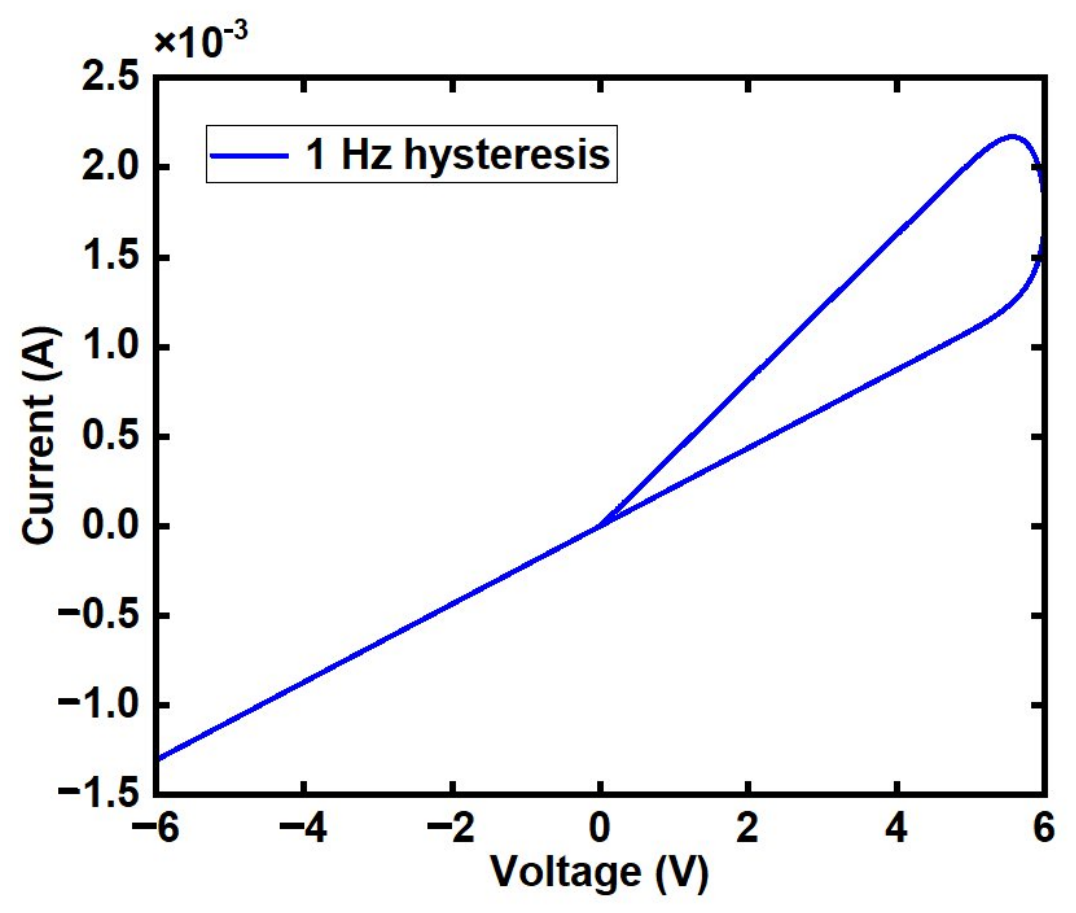
Figure 1. I-V pinched hysteresis loop of the VTEAM model under 1 Hz sinusoidal excitation.
Electronics 15 02333 g001
Figure 2. Resistance-state mapping of VTEAM and linear-drift models.
Electronics 15 02333 g002
Figure 3. Reset characteristics under the proposed two-phase read–write scheme, reaching 8681.68 Ω with a 90% settling time of 18.401 ms, in agreement with the analytical prediction of Equation (15).
Electronics 15 02333 g003
Figure 4. Set characteristics under the proposed two-phase read–write scheme, reaching 630.02 Ω with a 90% settling time of 16.766 ms.
Electronics 15 02333 g004
Figure 5. SPICE -level verification of the proposed two-phase timing under 65 nm-equivalent BSIM3 device models. The black dotted line indicates the analytical prediction from the behavioral-level simulation for direct comparison with the SPICE transient response.
Electronics 15 02333 g005
Figure 6. Mode-switching behavior of the PMOS/NMOS mutually exclusive read–write interface, verifying the mutual-exclusion invariant (Equation (21)) with write-mode activation from 0 to 20 ms and read-mode activation from 20 to 40 ms.
Electronics 15 02333 g006
Figure 7. SPICE-level verification of charge injection in the PMOS/NMOS mutually exclusive isolation topology, simulated in LTspice with 65 nm-equivalent BSIM3 device models, minimum-size pass transistors ( W / L = 130 nm / 65 nm), and effective node capacitance C node = 50 fF.
Electronics 15 02333 g007
Figure 8. Read–write characteristics of the linear-drift model under the same interface scheme, confirming stable state evolution under the shared timing framework and consistent with the charge-bound condition of Equation (22).
Electronics 15 02333 g008
Figure 9. Cycle-to-cycle consistency of the memristor under 10 alternating Reset/Set operations, with read-state fluctuations of 0.0042% and 0.0077%, both well within the analytical bound of Equation (23).
Electronics 15 02333 g009
Figure 10. Noise robustness under 100-run Monte Carlo perturbation with combined D2D ( σ D 2 D = 5 % ) and C2C ( σ C 2 C = 3 % ) variability, showing a mean read-current CV of 5.006% with a 95% confidence interval of [4.996%, 5.015%], in quantitative agreement with the analytical decomposition of Equation (25).
Electronics 15 02333 g010
Figure 11. Direct simulation of dynamic noise mechanisms layered onto the static D2D/C2C variability baseline.
Electronics 15 02333 g011
Figure 12. SPICE-level thermal verification of the proposed read–write interface across T amb [ 10 , + 85 ] °C with 65-nm-equivalent BSIM3 pass transistors and a temperature-coupled VTEAM cell.
Electronics 15 02333 g012
Figure 13. Average resistance variation of the two memristor models under different operating frequencies, showing 37.57 % VTEAM drift and + 6.71 % linear-drift change from 1 Hz to 20 Hz, consistent with the opposite-sign prediction of Equation (32).
Electronics 15 02333 g013
Figure 14. Switching-time characteristics of the memristor during Reset and Set operations, giving 3.158 ms and 4.752 ms 10–90% times with an asymmetry ratio of 1.504, consistent with the analytical prediction of Equation (33).
Electronics 15 02333 g014
Figure 15. Power and energy comparison between the proposed read–write separation interface and the no-separation baseline, showing 30.94% and 96.08% cycle-energy savings for Reset and Set, in close agreement with the analytical predictions of Equation (14).
Electronics 15 02333 g015
Figure 16. Effect of line parasitic resistance on the memristor I-V characteristics, with peak current drops of 1.912%, 3.750%, and 7.224% at 50, 100, and 200 Ω , bounded from above by the low-resistance limit of Equation (34).
Electronics 15 02333 g016
Table 1. Sensitivity of the EDA-optimal design point to the weighting vector ( λ E , λ D , λ A ) .
Scenario ( λ E , λ D , λ A ) V wr Reset / Set V rd T 90 Reset Δ E Reset / Set CV ( I rd ) MNIST Top-1
Balanced (default) ( 0.33 , 0.33 , 0.33 ) + 6.5 / 5.5  V 1.0  V 18.4  ms 30.9 % / 96.1 % 5.01 % 90.6 %
Energy-priority ( 0.7 , 0.15 , 0.15 ) + 6.0 / 5.0  V 1.0  V 21.7  ms 38.6 % / 96.9 % 5.30 % 90.3 %
Delay-priority ( 0.15 , 0.7 , 0.15 ) + 7.0 / 6.0  V 1.0  V 14.3  ms 23.1 % / 95.2 % 5.01 % 90.6 %
Accuracy-priority ( 0.15 , 0.15 , 0.7 ) + 6.5 / 5.5  V 0.9  V 18.4  ms 28.7 % / 95.6 % 4.74 % 90.9 %
Extreme-energy ( 0.9 , 0.05 , 0.05 ) + 5.8 / 4.8  V 1.0  V 24.9  ms 42.1 % / 97.2 % 5.52 % 89.9 %
Table 2. MNIST-style top-1 accuracy of the 784 × 10 crossbar with directly simulated dynamic-noise mechanisms layered onto the static D2D/C2C variability baseline.
ConfigurationTop-1 AccuracyDegradation vs. SW
Software baseline91.8%
+ Static D2D + C2C variability90.6%1.2%
+ Directly simulated RTN90.2%1.6%
+ RTN + state relaxation (100 s window)89.7%2.1%
+ All above + R line = 100 Ω parasitics89.3%2.5%
Disclaimer/Publisher’s Note: The statements, opinions and data contained in all publications are solely those of the individual author(s) and contributor(s) and not of MDPI and/or the editor(s). MDPI and/or the editor(s) disclaim responsibility for any injury to people or property resulting from any ideas, methods, instructions or products referred to in the content.