Article

A 3.3–8.0 GHz Wideband LNA with a 0.81–1.09 dB Noise Figure in 0.15 µm GaAs pHEMT Technology
1
Department of Mobile Convergence Engineering, Hanbat National University, Daejeon 34158, Republic of Korea
2
Department of Semiconductor Systems Engineering, Hanbat National University, Daejeon 34158, Republic of Korea
*
Authors to whom correspondence should be addressed.
Electronics 2026, 15(11), 2259; https://doi.org/10.3390/electronics15112259
Submission received: 10 April 2026 / Revised: 15 May 2026 / Accepted: 21 May 2026 / Published: 23 May 2026
(This article belongs to the Special Issue RF/Microwave Integrated Circuits Design and Application)

Abstract

This paper presents the design and fabrication of a wideband low-noise amplifier (LNA) covering C-band, using the 0.15 µm GaAs pHEMT process. To achieve both low noise performance and wide matching characteristics, a two-stage cascaded architecture is implemented. In the first stage, circular inductors and an inductive source degeneration technique are employed to minimize the noise figure (NF) while ensuring wideband input matching. Furthermore, an RC feedback structure is incorporated to effectively enhance the stability of the amplifier. The proposed LNA operates under a supply voltage of 3.3 V and a gate bias of 0.35 V, with a total DC power consumption of 69.3 mW. The fabricated MMIC occupies a total chip area of 1.98 mm2, including the probing pads. Measurement results demonstrate that the LNA achieves an NF of 0.81–1.09 dB and a gain of over 20.1 dB in the frequency range of 3.3–8.0 GHz. The input and output return losses are maintained over 10 dB and 9.7 dB, respectively.

1. Introduction

Recent advances in radio frequency (RF) technology have enabled its widespread application in various fields, including satellite communications, fifth generation (5G) mobile infrastructure, automotive and military radar systems, and high-resolution remote sensing. Among these, the S-band (2–4 GHz) is widely utilized in long-range radar and air traffic control (ATC) systems, as it offers an optimal balance between antenna size and atmospheric attenuation, ensuring reliable performance even under adverse weather conditions [1]. In contrast, the C-band (4–8 GHz) offers an advantageous balance between coverage range and spatial resolution, making it highly suitable for applications such as weather monitoring, military radar detection, and broadband wireless communications [2]. In such applications, the low-noise amplifier (LNA) serves as a critical building block in the receiver front-end, as it amplifies weak incoming signals while largely determining the overall system performance, particularly the noise figure (NF). Since the LNA is positioned at the initial stage of the receiver chain, its noise contribution directly impacts the sensitivity of the entire system.
In this work, a two-stage LNA monolithic microwave integrated circuit (MMIC) operating in the C-band and a portion of the S-band is designed using the 0.15 µm GaAs pHEMT process. The main contributions of this work are summarized as follows. (1) Simultaneous wideband matching and noise minimization: A two-step matching technique based on inductive source degeneration and gate inductor optimization is employed. Furthermore, high-Q circular inductors are strategically utilized exclusively in the first stage to tightly suppress thermal noise contributions, thereby enhancing the overall NF performance. (2) Analytical design for wideband gain flatness: Unlike conventional GaAs LNAs that often rely on empirical tuning, this work systematically optimizes gain flatness. Specifically, the output matching network (OMN) is designed based on a rigorous voltage gain analysis, securing a highly flat gain response across a wide frequency range. (3) Systematic optimization of multi-dimensional trade-offs: The complex trade-offs among linearity, gain, and stability are comprehensively analyzed. Rather than utilizing trial-and-error methodologies, these parameters are analytically optimized through source degeneration to achieve a robust and reliable design. (4) Highly competitive wideband performance: As a result of the proposed analytical approaches and structural advantages, the implemented LNA achieves wideband impedance matching across the entire operating bandwidth. Notably, it maintains an exceptionally low noise profile, with a NF ranging from 0.81 dB to 1.09 dB.

2. The 0.15 µm GaAs pHEMT Process

In this paper, the PE15 process provided by WIN Semiconductors is employed. This technology is a GaAs-based enhancement-mode pseudomorphic high electron mobility transistor (pHEMT) MMIC process featuring a 0.15 µm gate length [3]. It is specifically developed for high-frequency RF and millimeter-wave circuit applications, with a nominal operating voltage of approximately 4 V. The process is well suited for the implementation of key RF building blocks, including LNAs, switches, mixers, and integrated RF front-end modules.
A pHEMT employs a pseudomorphic heterojunction to confine carriers, thereby forming a high-mobility two-dimensional electron gas (2DEG). An InGaAs-based channel provides high electron mobility, enabling a large transconductance (gm) and enhanced RF performance in terms of gain and noise.
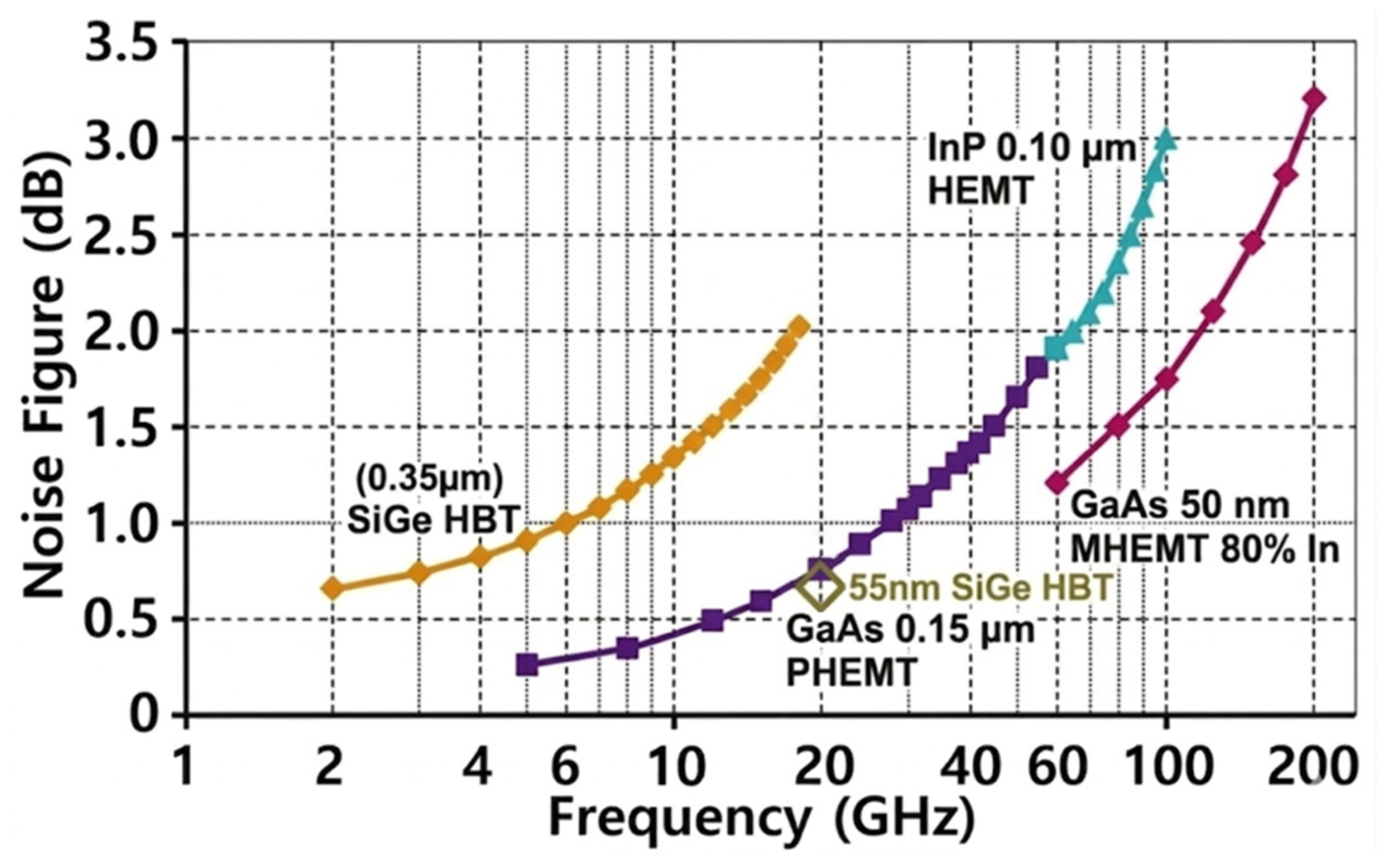
Figure 1 compares the NF performance across various process technologies. The 0.15 µm GaAs pHEMT process, utilized in LNA designs, facilitates high gain and minimal noise, offering enhanced high-frequency performance owing to its exceptional carrier mobility.

3. Active Device and Bias Selection

In the first step of LNA design, the selection of the active device is a key factor that determines the trade-off among NF, gain, and linearity. The 0.15 µm pHEMT process offers two transistor structures: Microstrip (MS) and Coplanar Waveguide (CPW) [5]. The CPW structure places the ground on the same plane as the signal line, thereby minimizing the parasitic inductance introduced by via-holes and providing favorable characteristics at high frequencies. Therefore, the CPW transistor structure was adopted in this work because it facilitates the implementation of inductive source degeneration for input impedance matching and noise performance improvement.
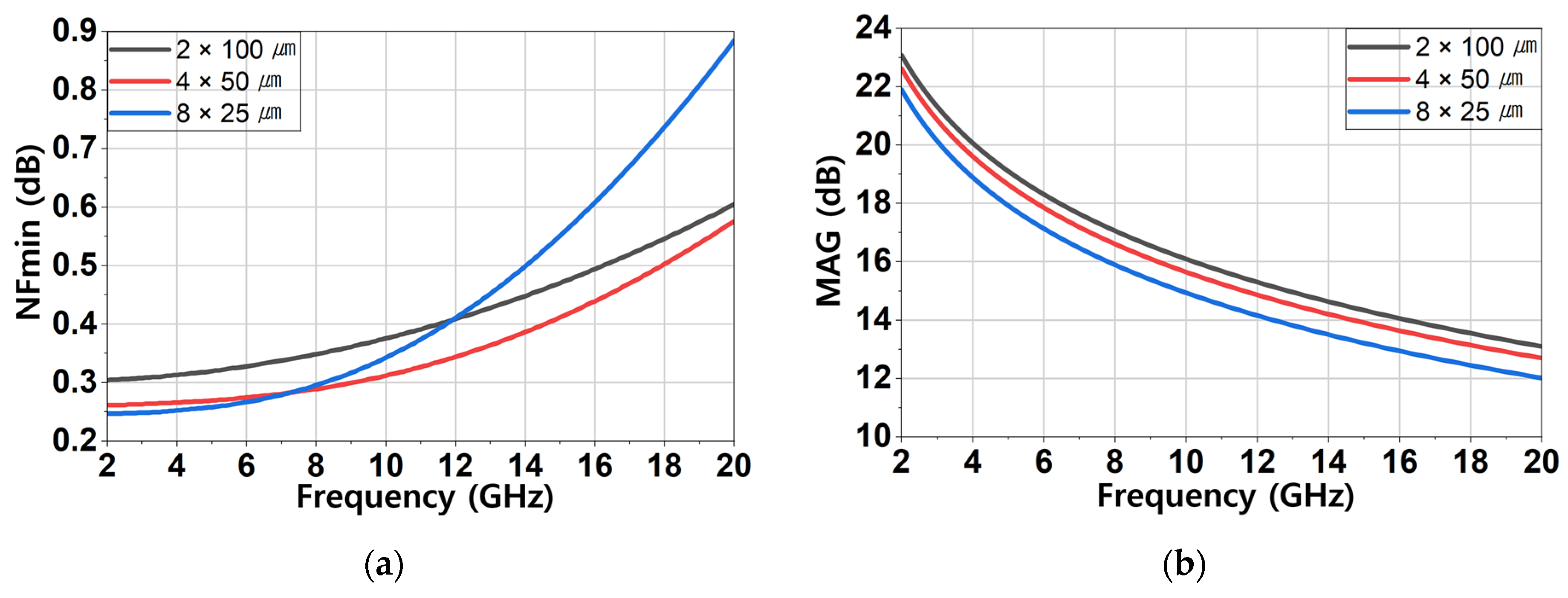
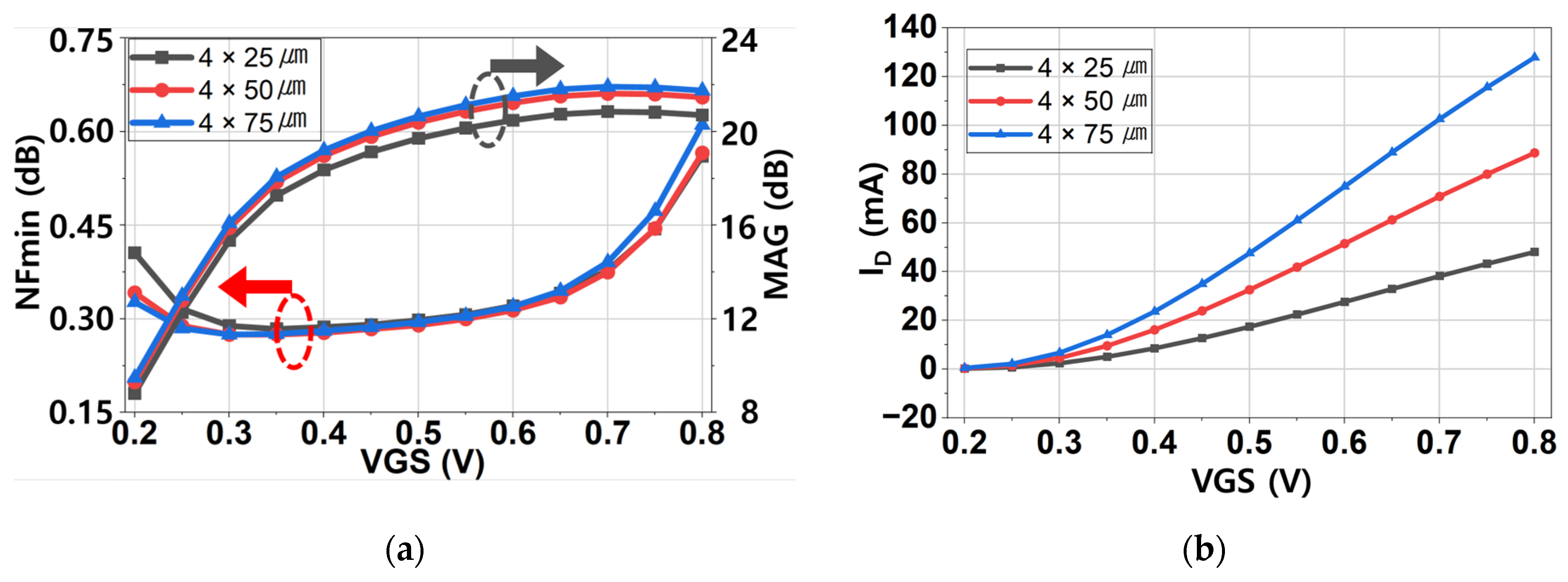
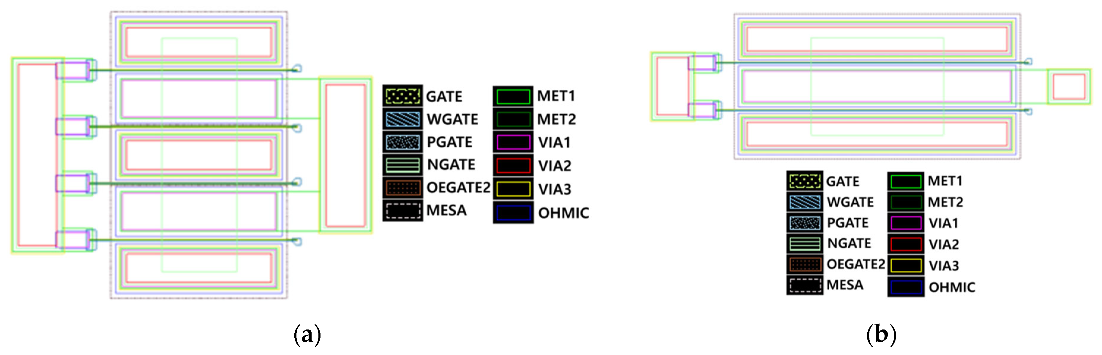
Table 1 summarizes the simulated RF performance of the transistors with different total gate widths at 6 GHz. To investigate the influence of device geometry, the total gate width was fixed at 100 µm, 200 µm, and 300 µm, while both two-finger and four-finger configurations were evaluated. The corresponding minimum noise figure (NFmin), maximum available gain (MAG), and drain current at VGS = 0.35 V were extracted to examine the relationship between the transistor structure and its RF performance. Based on the results, the transistors with a total gate width of 200 µm were selected for further analysis. Figure 2a,b illustrate the simulated NFmin and MAG over the frequency range of 2–20 GHz under gate bias conditions of VGS = 0.35 V and VDD = 3.3 V. As shown in Figure 2a,b, the 4 × 50 µm configuration maintains a comparable NFmin to that of the 8-finger configuration while achieving a higher MAG exceeding 16 dB across the operating frequency band. Based on this result, the number of fingers was fixed to four for further analysis. The device performance was analyzed by varying the finger width while maintaining the same finger number. To validate the device characteristics, additional simulations were performed at 6 GHz by sweeping VGS from 0.2 V to 0.8 V, as shown in Figure 3a. Figure 3a shows that the 4 × 50 µm device achieves an NFmin lower than 0.29 dB and a MAG higher than 16.6 dB over the 3.3–8.0 GHz frequency range while maintaining an appropriate current level that satisfies the design requirements. The corresponding drain current variation under identical bias conditions is presented in Figure 3b. Based on these results, the 4 × 50 µm device was selected as the optimal transistor for the proposed LNA. The optimal operating condition was determined with VGS = 0.35 V, where an NFmin of 0.275 dB was achieved. In addition, different device sizes were employed according to the role of each amplification stage. Figure 4a shows the 4 × 50 µm CPW transistor used in the first stage, while Figure 4b illustrates the 2 × 100 µm CPW transistor adopted in the second stage. The process-layer color labels used in the layouts have also been added for clarity. The detailed rationale for selecting the second-stage transistor size is discussed in Section 4.

4. Design of the LNA

4.1. Inductive Source Degeneration and Matching

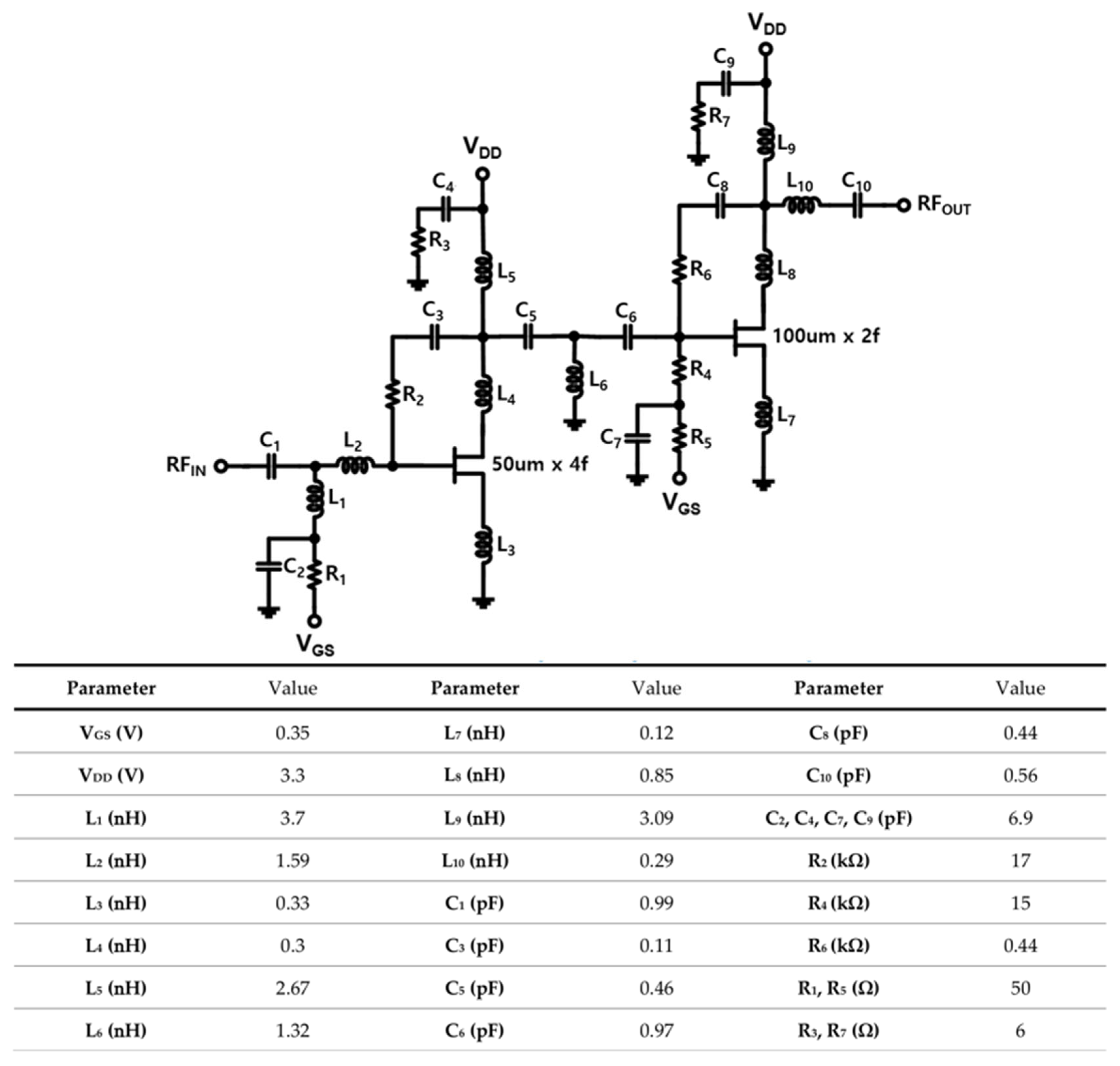
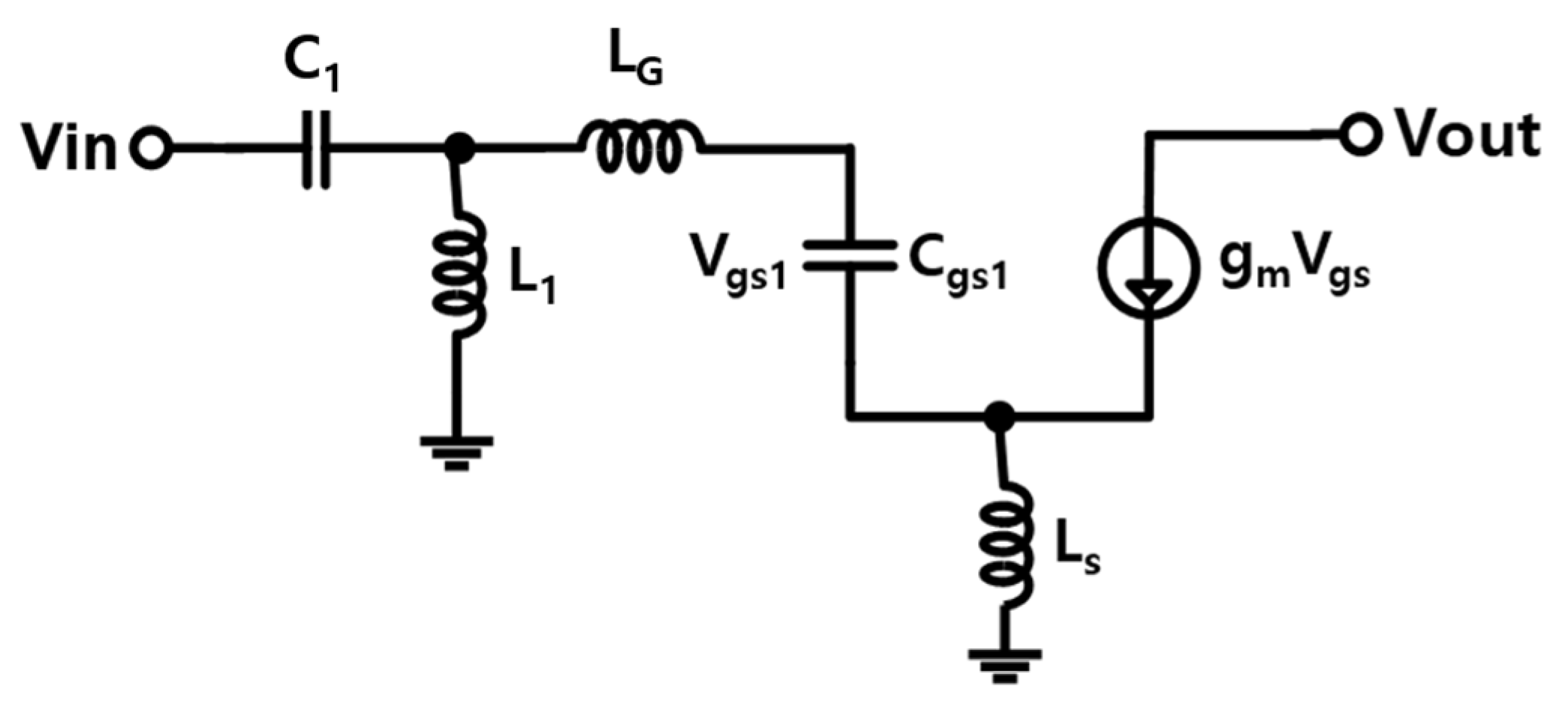
Section 4 presents the circuit design methodology and detailed analysis of the proposed LNA. Figure 5 presents the overall schematic of the proposed LNA, including the detailed passive component values and bias conditions used in this design. Concurrent optimization of noise and input matching is a key consideration in LNA design. In this work, an inductive source degeneration technique is employed to achieve both simultaneously [6]. Figure 6 shows the equivalent circuit of the input stage used for analysis. For simplicity, the effect of the RC feedback network is neglected in this equivalent model. Based on this model, the total input impedance seen from the input port can be expressed as in (1). The first term represents the intrinsic gate–source capacitance   C g s of the transistor, while the second term corresponds to the reactive components introduced by the gate inductor L G and source inductor L S . The key feature of this structure lies in the final term, which represents the real part g m L s / C g s . This indicates that the desired matching impedance can be achieved by adjusting the value of the source inductor L S without incorporating a physical resistive element. Consequently, impedance matching can be realized while avoiding additional thermal noise, thereby maintaining the NFmin [7].
Z i n s = 1 s C g s + s L G + L S + g m L S C g s
Furthermore, the frequency-dependent impedance of the inductor increases with frequency. As a result, the inductor presents a larger impedance at higher frequencies, which helps suppress excessive high-frequency components that may otherwise be amplified. This behavior mitigates potential oscillations caused by parasitic capacitances and internal feedback paths of the transistor, thereby improving the overall circuit stability [8]. In addition, compared with resistive matching networks, the inductive matching approach provides improved voltage headroom, which is beneficial for low-power operation and linearity.
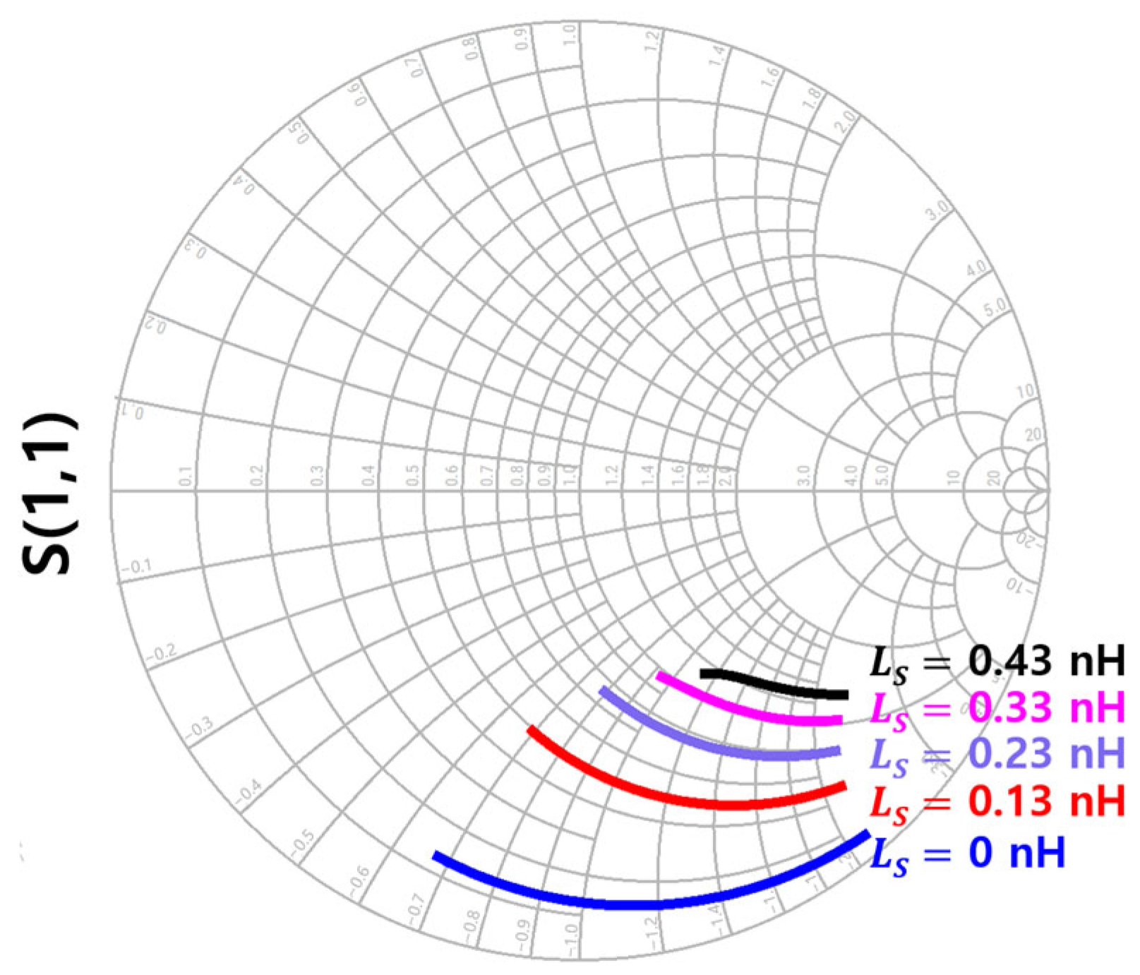
To simultaneously optimize input matching and noise performance, a two-step matching procedure is adopted [9]. In the first step, the effect of L S on the input impedance is investigated by sweeping its value, as shown in Figure 7. The results indicate that the input impedance varies significantly with the value of L S . In particular, when L S is set to 0.33 nH, the input impedance is closest to 50 Ω at the target operating frequency, providing the best input matching performance. Therefore, the value of L S is selected as 0.33 nH in this design.
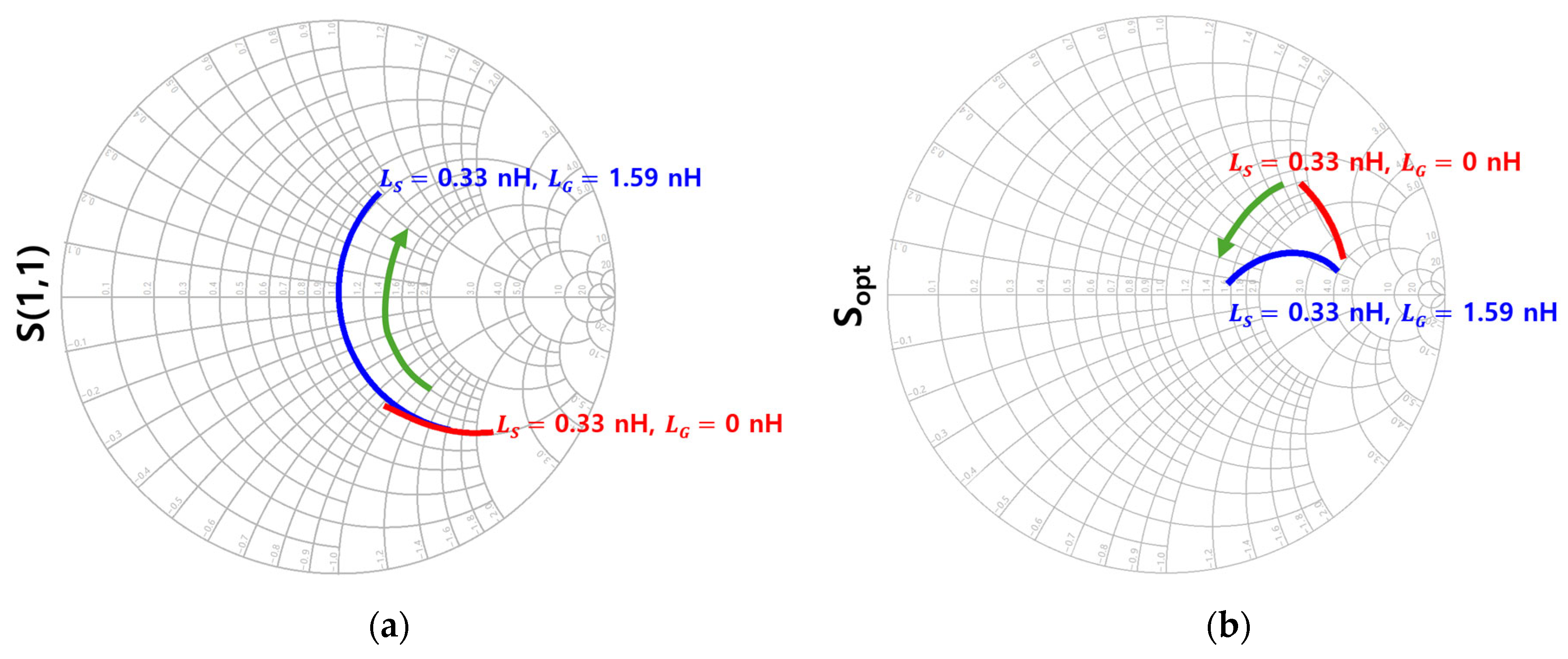
However, while L S strongly influences the movement of the input impedance, it has a relatively limited effect on the position of the optimum noise impedance (Sopt) [10]. Therefore, in the second step, the gate inductor L G is adjusted to simultaneously optimize input matching and noise performance. As illustrated in Figure 8a, the input impedance approaches 50 Ω as L G is tuned, and the optimal value of L G is determined to be 1.59 nH. In addition, Figure 8b presents the variation of Sopt, which also shifts toward the 50 Ω region with the same value of L G . These results indicate that appropriate tuning of L G simultaneously improves both input and noise matching. Through this approach, both input matching and noise performance can be optimized using the combined effects of L s and L G .
F t o t a l = F 1 + F 2 1 G 1 + F 3 1 G 1 G 2 + · · · + F n 1 G 1 G 2 · · · G n 1
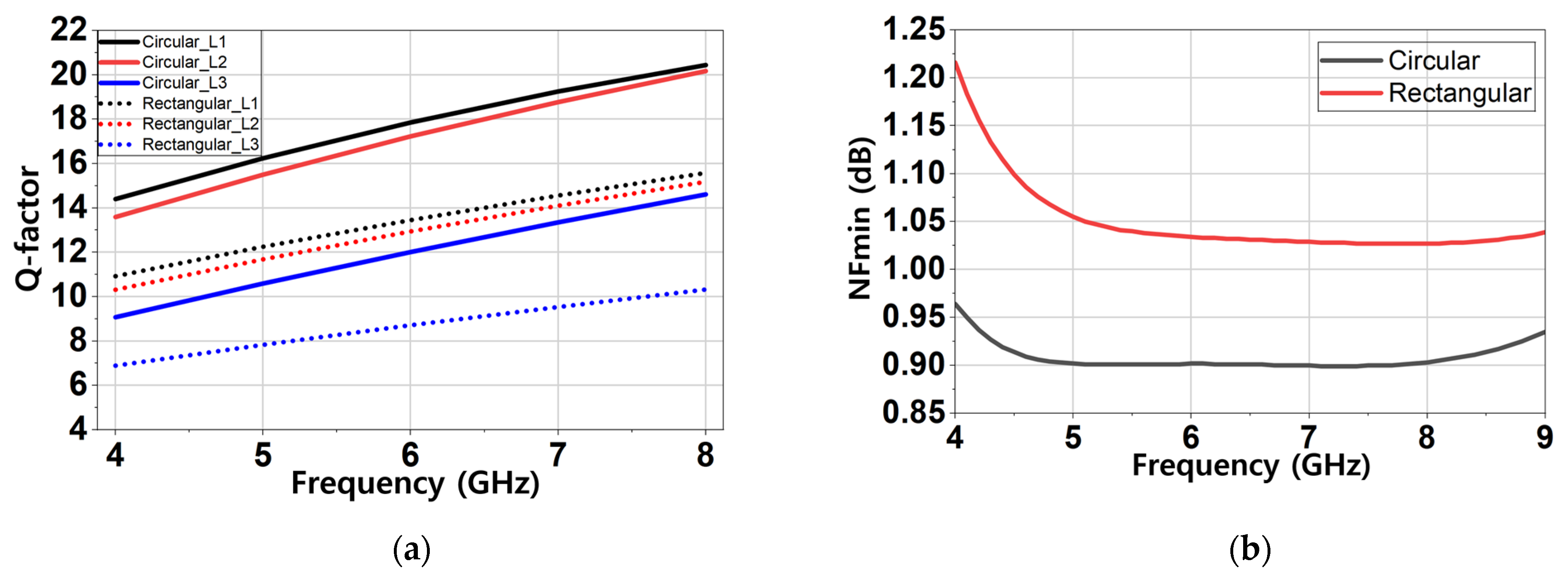
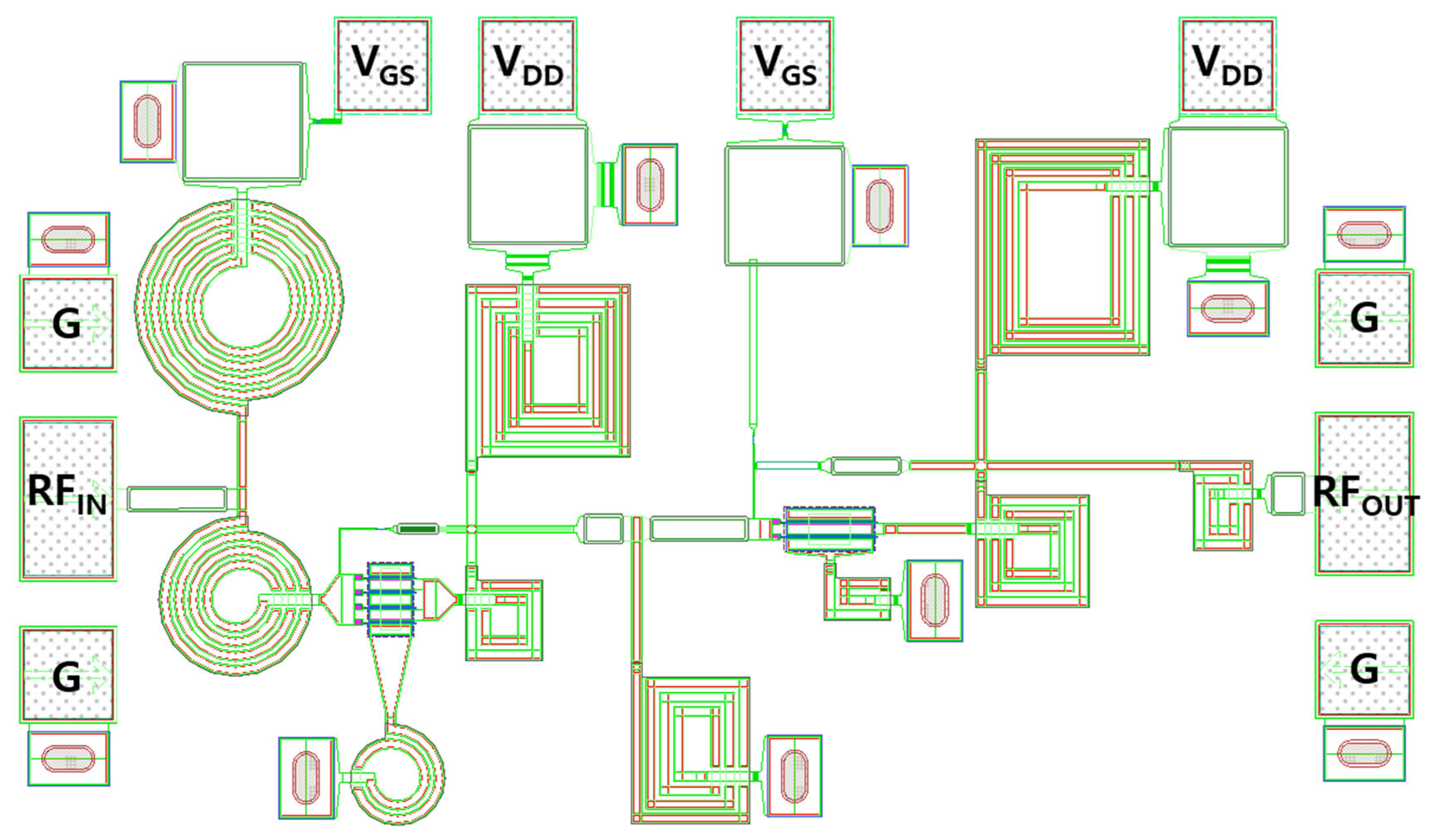
According to the Friis equation for cascaded stages shown in (2), the overall NF is primarily determined by the noise contribution of the first stage F 1 . Therefore, minimizing the noise contribution of the first stage is essential for improving the overall NF performance. Accordingly, circular inductors are employed in the first stage of the proposed LNA. Figure 9a shows the simulated Q-factor of circular and rectangular inductors with the same inductance values as those used in the proposed LNA design. The circular inductors exhibit Q-factors ranging from 9.07 to 20.44, whereas the rectangular structures show Q-factors between 6.89 and 15.58. The higher Q characteristics effectively reduce losses caused by parasitic resistance, which in turn lowers the noise contribution of the input stage. Figure 9b shows the simulated NF performance as a function of the inductor geometry in the first stage. The simulation results indicate that circular inductors exhibit approximately 0.3 dB lower NF compared with rectangular inductors. As a result, the overall noise performance of the LNA is improved. Figure 10 illustrates the final layout of the proposed LNA, in which circular inductors are selectively employed in the first stage to enhance performance.
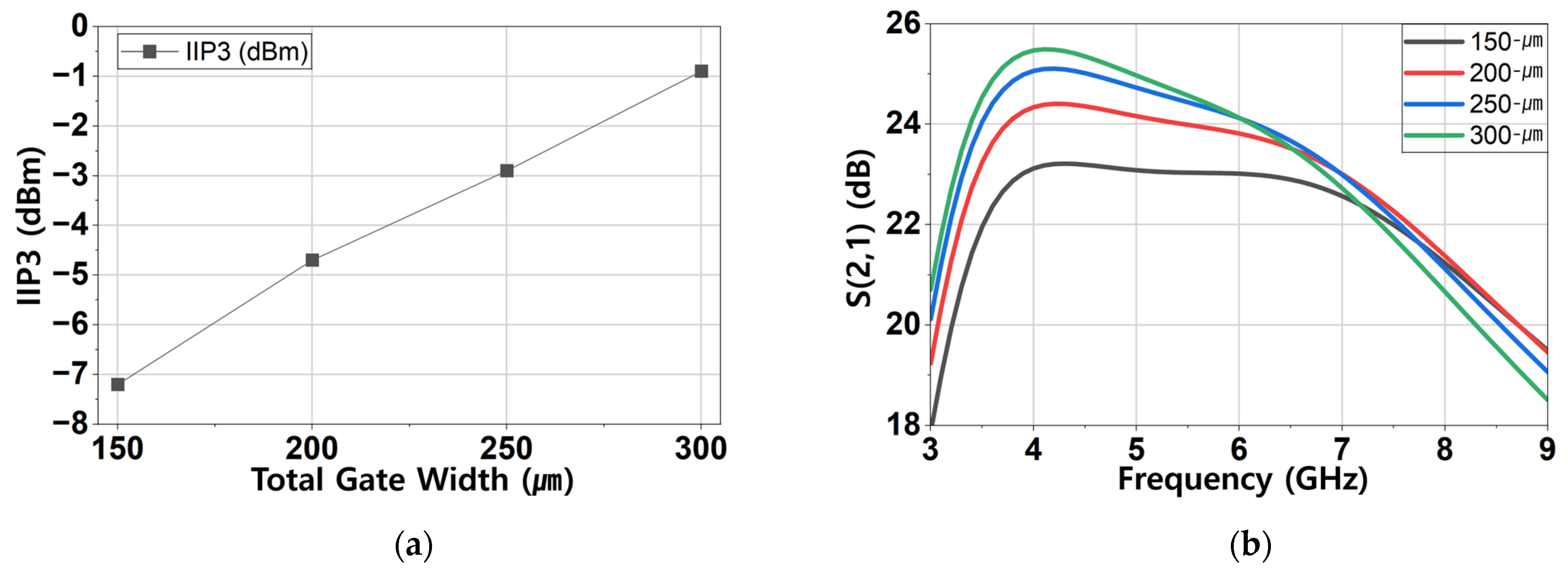
Following the optimization of the noise performance in the first stage, the second stage is further designed to maximize the overall linearity, gain flatness, and stability of the LNA. Since the transistor size in the second stage is a determining factor in the balance between gain and linearity, the total gate width was swept to investigate its impact on the circuit performance. Figure 11a shows the simulated IIP3 at 6 GHz, indicating that the linearity improves as the total gate width increases, achieving values higher than −5 dBm. However, as shown in Figure 11b, although the low-frequency gain increases with larger device size, the high-frequency gain starts to degrade when the total gate width exceeds 250 µm due to increased parasitic capacitances. Therefore, a total gate width of 200 µm was selected as an optimal trade-off between linearity and gain flatness. In addition, as observed in Figure 2b, a two-finger configuration exhibits higher gain compared to a four-finger structure and provides more favorable parasitic characteristics, such as gate resistance ( r g ) and output resistance ( r o ), which facilitate impedance matching. Based on these considerations, a 2 × 100 µm transistor size was finally adopted for the second stage.
The effect of source degeneration on linearity, gain, and stability can be characterized by the effective transconductance expression derived in (3) [7]:
G m = g m 1 ω 0 C g s   R s + ω T L s
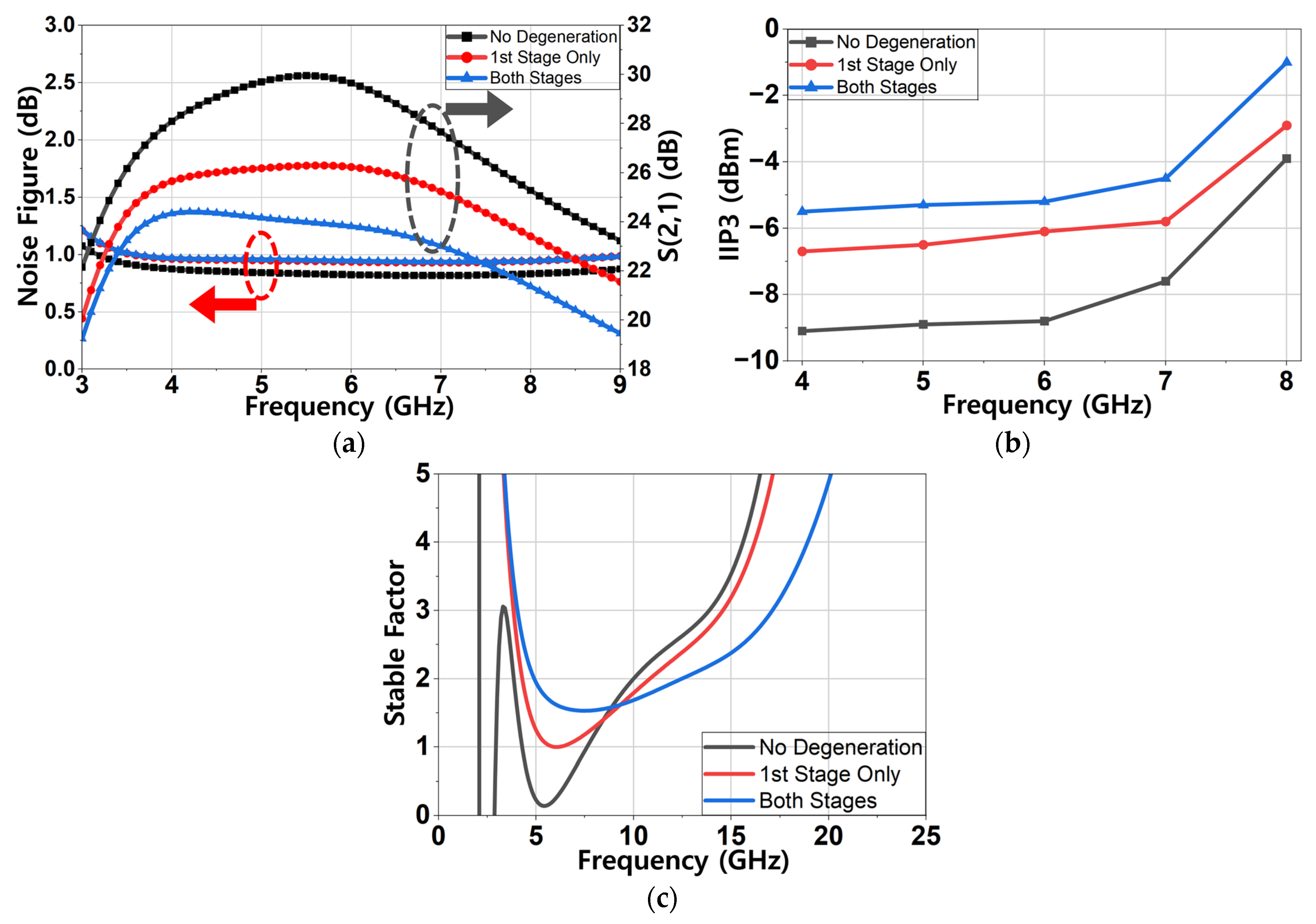
where g m 1 is the intrinsic transconductance, Rs is the source resistance, ω 0   is the operating angular frequency, and ω T is the transition frequency. As indicated in (3), the introduction of L s increases the denominator through the ω T L s term, which represents the input resistance generated by the negative feedback. This results in a reduction of the overall transconductance ( G m ), suppressing nonlinear distortion at the expense of gain. To verify this trade-off, Figure 12 compares three configurations: without L s , with L s   in the first stage only, and with L s   in both stages. As shown in Figure 12a, applying L s to both stages slightly increases the NF by approximately 0.1 dB compared to the first stage-only case, primarily due to the decrease in gain by the L s . However, the gain remains above 20 dB across the 3.3–8.0 GHz band with a more uniform response. The improvement in linearity is clearly observed in Figure 12b, which compares the IIP3 performance among different configurations. The results demonstrate that applying L s to both stages achieves the highest IIP3 across the entire frequency band, which is consistent with the theoretical analysis [7]. In contrast, the configuration without L s exhibits a lower IIP3, dropping to −9 dBm in the low-frequency range. These results indicate that the dual-stage source degeneration is highly effective in maintaining robust linearity throughout the target bandwidth. Furthermore, as shown in Figure 12c, L s enhances the stability by providing local feedback, confirming the inherent trade-off between gain and stability. Consequently, the proposed design adopts optimized source degeneration inductance of L 3 = 0.33 nH and L 7 = 0.12 nH in the schematic of Figure 5, achieving a balanced performance in terms of stability, gain flatness, and linearity.

4.2. Analysis and Optimization of the Output Matching Network

To further elucidate the broadband matching mechanism, the output impedance ( Z o u t ) of the proposed network can be derived as Equation (4):
Z o u t = ( s L 10 + 1 s C 10 ) + [ ( s L 9 | | ( s L 8 + 1 s C d 2 ) ) | | ( 1 s C 8 + R 6 ) ]
Equation (4) comprehensively illustrates the strategic role of each matching component. The initial series term acts as a resonant network to precisely match the final impedance to 50 Ω. Within the parallel core section, L 9   functions as an RF choke by providing high impedance, while L 8 is introduced to resonate with and compensate for the large parasitic capacitance ( C d 2 ) of the transistor, which otherwise degrades Z o u t . The concurrent utilization of L 8 and L 9 for   C d 2 compensation dictates a fundamental design trade-off among the bandwidth, chip area, and gain.
Moreover, the parallel RC feedback branch intricately governs the stability and gain profile. The resistor R 6 determines the overall feedback strength; a reduced R 6 enforces stronger feedback, which enhances stability but penalizes the total gain and NF. Conversely, an excessive R 6 limits the bandwidth and heavily risks oscillation by dropping the K-factor below unity. Concurrently, C 8 is tailored to control low-frequency stability. A deficient C 8 acts as an open circuit at lower frequencies, thereby weakening the feedback and inducing an excessive low-frequency gain that plunges the K-factor below 1. Therefore, an adequately sized C 8 is imperative to suppress the low-frequency gain and ensure unconditional stability. These physical impedance characteristics directly translate into the voltage gain profile. The output matching network (OMN) shown in Figure 5 consists of L 8 , L 9 , L 10 , and C 10 , playing a pivotal role in enhancing both gain and linearity. In this work, an OMN gain analysis approach is employed to systematically investigate the contribution of each component. The analytical expression for the small-signal voltage gain ( A o ) of the proposed two-stage cascaded common-source LNA is given in (5). From the numerator of A V 2 in (5), it is observed that these OMN parameters directly influence the second stage gain, which large governs the overall performance. Therefore, precise optimization of these values is essential to achieve a stable gain exceeding 20 dB.
A o = j ω g m 1 L 4 g m 1 R 2 + 1 j ω C 3   | |   j ω L 5   | | 1 j ω C 5 + j ω L 6   | |   1 j ω C 6 + R 4   | |   R 6 + 1 j ω C 8 1 + j ω g m 1 L 3 A V 1           × j ω g m 2 L 8 g m 2 R 6 + 1 j ω C 8   | |   j ω L 9 j ω g m 2 L 10 g m 2 j ω C 10 1 + j ω g m 2 L 7 A V 2
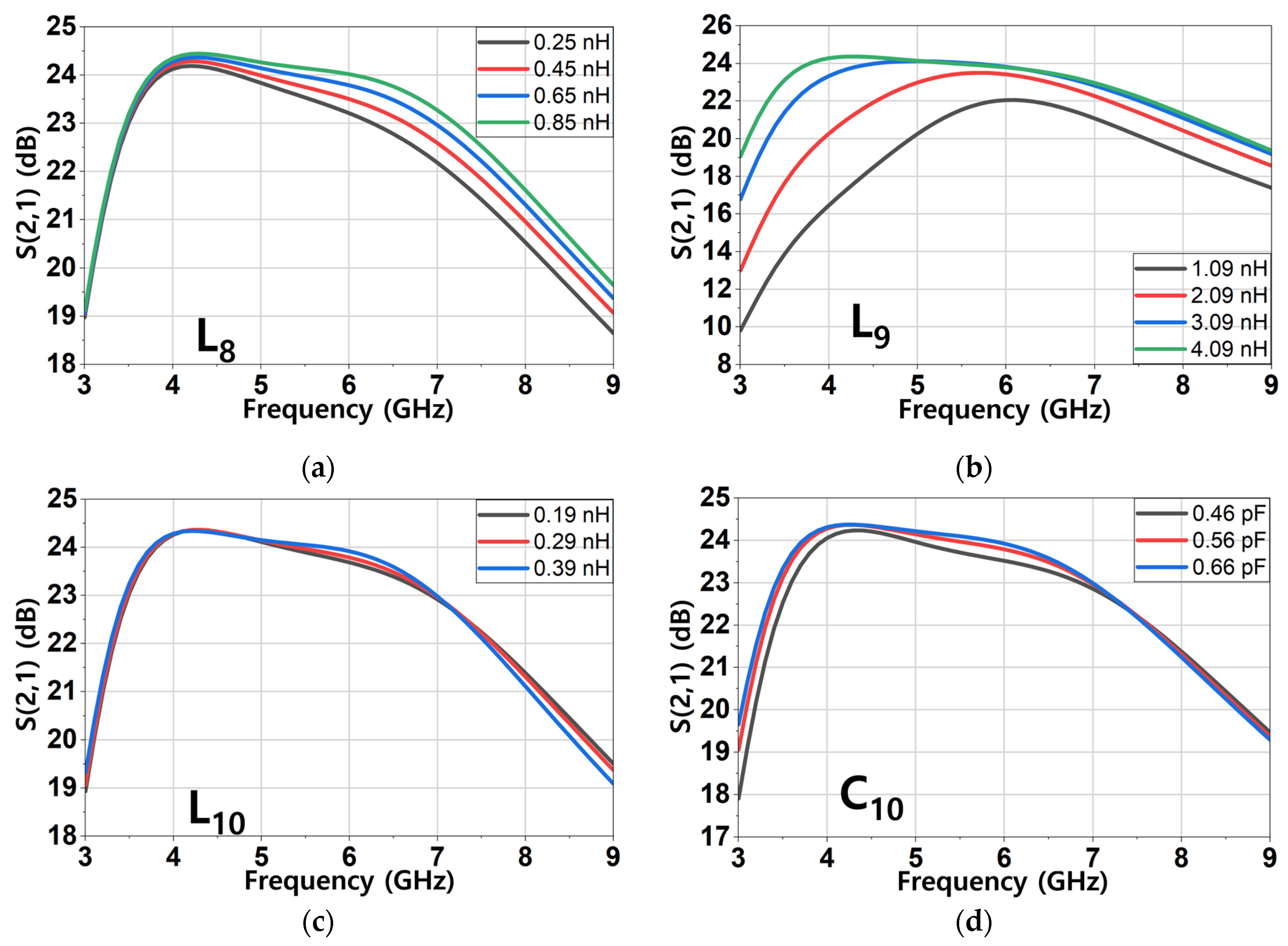
Regarding the primary gain detection, L 8 and L 9 function as the main load components. Inductor L 8 forms a resonance with the parasitic capacitance of the transistor at high frequencies, thereby selectively enhancing the gain in the upper region [11]. As shown in Figure 13a, L 8 effectively boosts high-frequency gain. However, exceeding 0.89 nH triggers in-band resonance below 8 GHz, degrading the matching condition (S(2,2) > −10 dB). Similarly, as illustrated in Figure 13b, L 9 serves as an RF choke and determines the drain load impedance. While reducing L 9 lowers low-frequency gain, an excessively large value (e.g., 4.09 nH) introduces undesirable peaking around 4 GHz. Consequently, L 8 and L 9 were optimized to 0.85 nH and 3.09 nH, respectively, to maintain a high gain profile without compromising matching or stability.
The gain flatness is further refined through the strategic adjustment of L 10 and C 10 . L 10 controls the impedance profile in the mid-frequency region by exploiting its inductive reactance X L = 2 π f L . As shown in Figure 13c, L 10 primarily alters the slope of the gain response rather than its magnitude, resulting in the selection of 0.29 nH to balance low-frequency suppression and high-frequency transmission [12]. Simultaneously, C 10 acts as a DC-blocking capacitor while compensating for the low-frequency matching variations introduced by L 10 . Its capacitive reactance X C = 1 / 2 π f C mitigates gain roll-off at lower frequencies, as demonstrated in Figure 13d. By choosing C 10 = 0.56 pF, the trade-off between insufficient compensation and excessive loading was successfully resolved.
As a result, the proposed design achieves a gain higher than 20 dB, with a flatness of ±1.9 dB across the operating band. Furthermore, since L 10 and C 10 provide fine-tuning rather than primary gain control, the OMN structure maintains high robustness against process variations, ensuring stable and reliable performance.
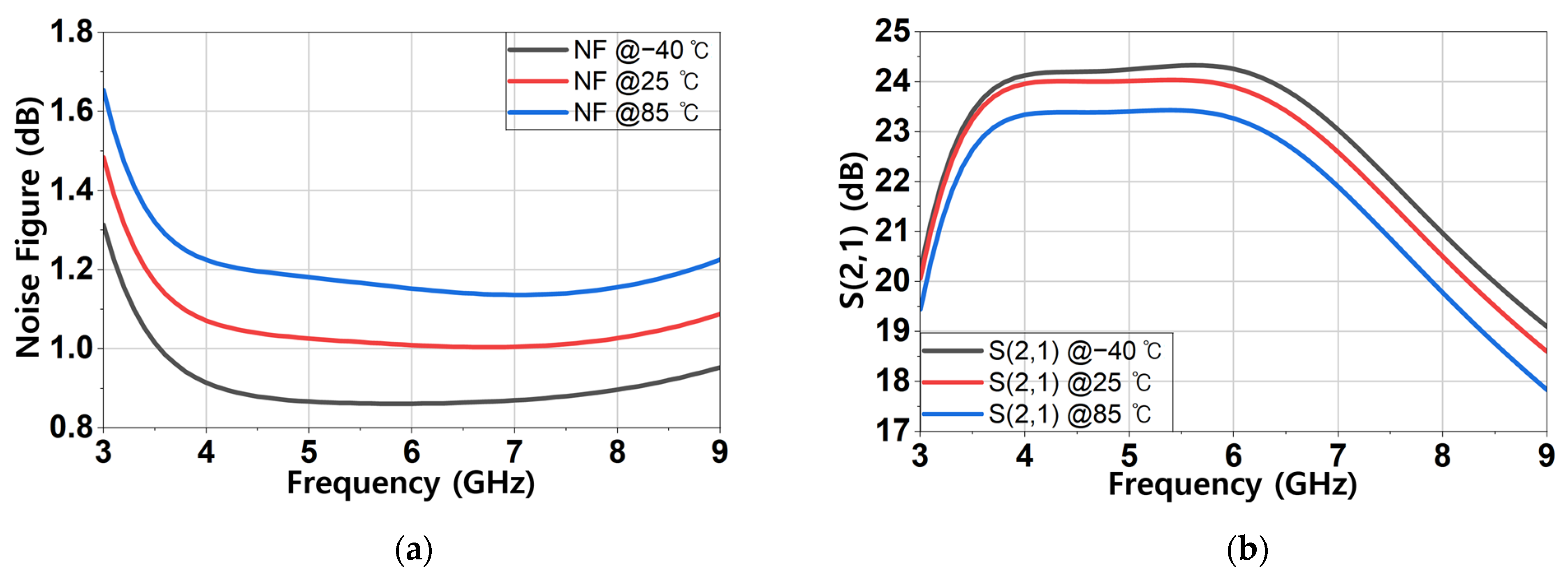
To further substantiate this reliability and rigorously assess the practical applicability of the proposed LNA, comprehensive temperature simulations were conducted over a standard industrial temperature range from −40 °C to 85 °C [13]. Figure 14a illustrates the simulated NF under varying temperature conditions, where the NF at 85 °C exhibits a marginal increase of approximately 0.3 dB compared to that at −40 °C. Similarly, as depicted in Figure 14b, the S(2,1) demonstrates a minor reduction of roughly 1 dB at 85 °C relative to the −40 °C condition. These robust thermal characteristics firmly verify the environmental and operational reliability of the proposed design, explicitly demonstrating its suitability for practical system integration applications.
To ensure stable operation over a wide frequency range, an RC feedback network is employed [14]. The stability factor (K-factor) is a widely recognized metric for evaluating the unconditional stability of RF circuits, which is defined as follows:
K = 1 S 11 2 S 22 2 + Δ 2 2 S 12 S 21
Δ = S 11 S 22 S 12 S 21
where S 11 and S 22 represent the input and output reflection coefficients, while S 21 and S 12 denote the forward gain and reverse transmission, respectively. The parameter Δ in (7) characterizes the interaction between the input and output ports. A circuit is considered unconditionally stable when K > 1 as expressed in (6), confirming that stability is maintained for any passive source and load impedances.
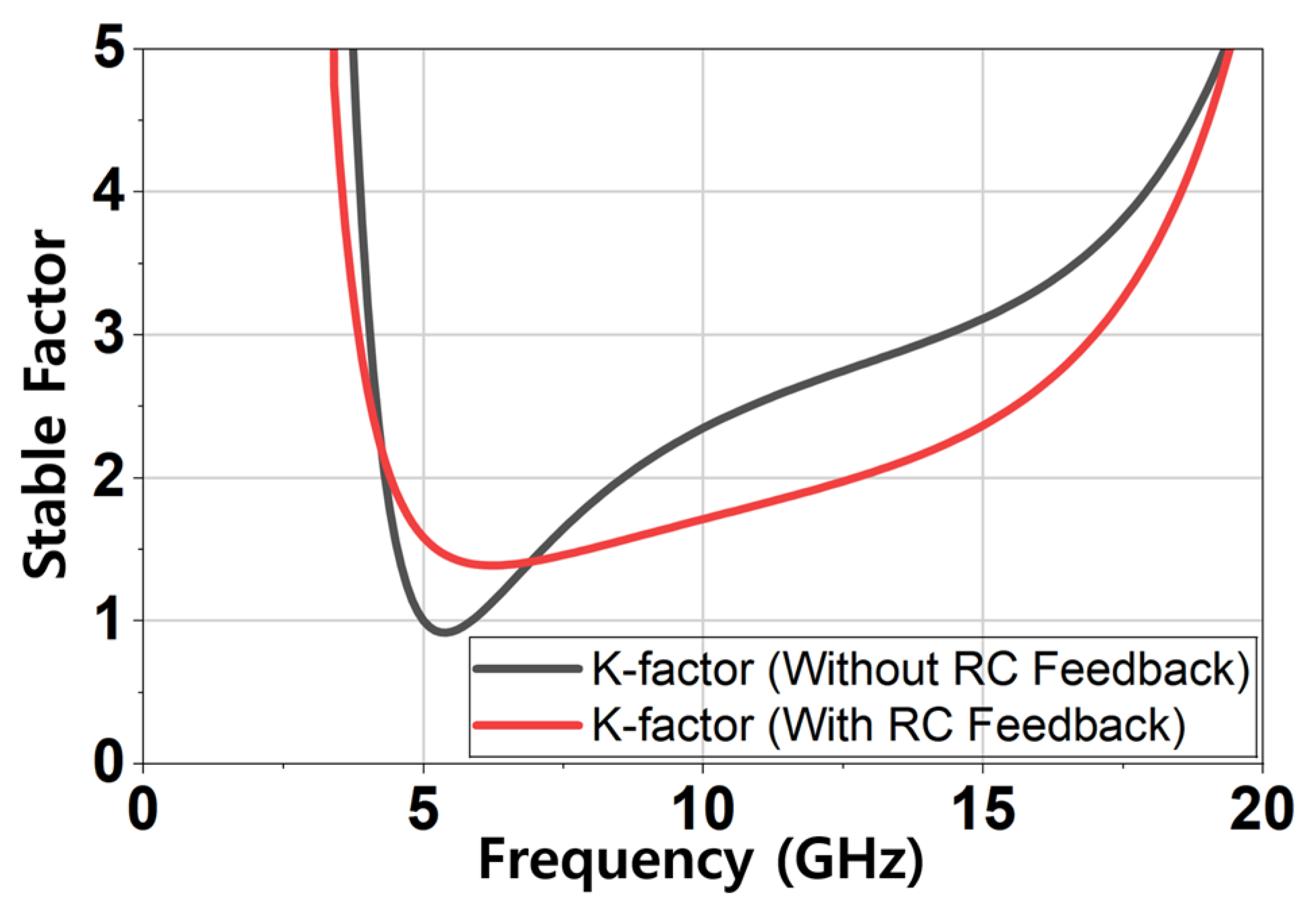
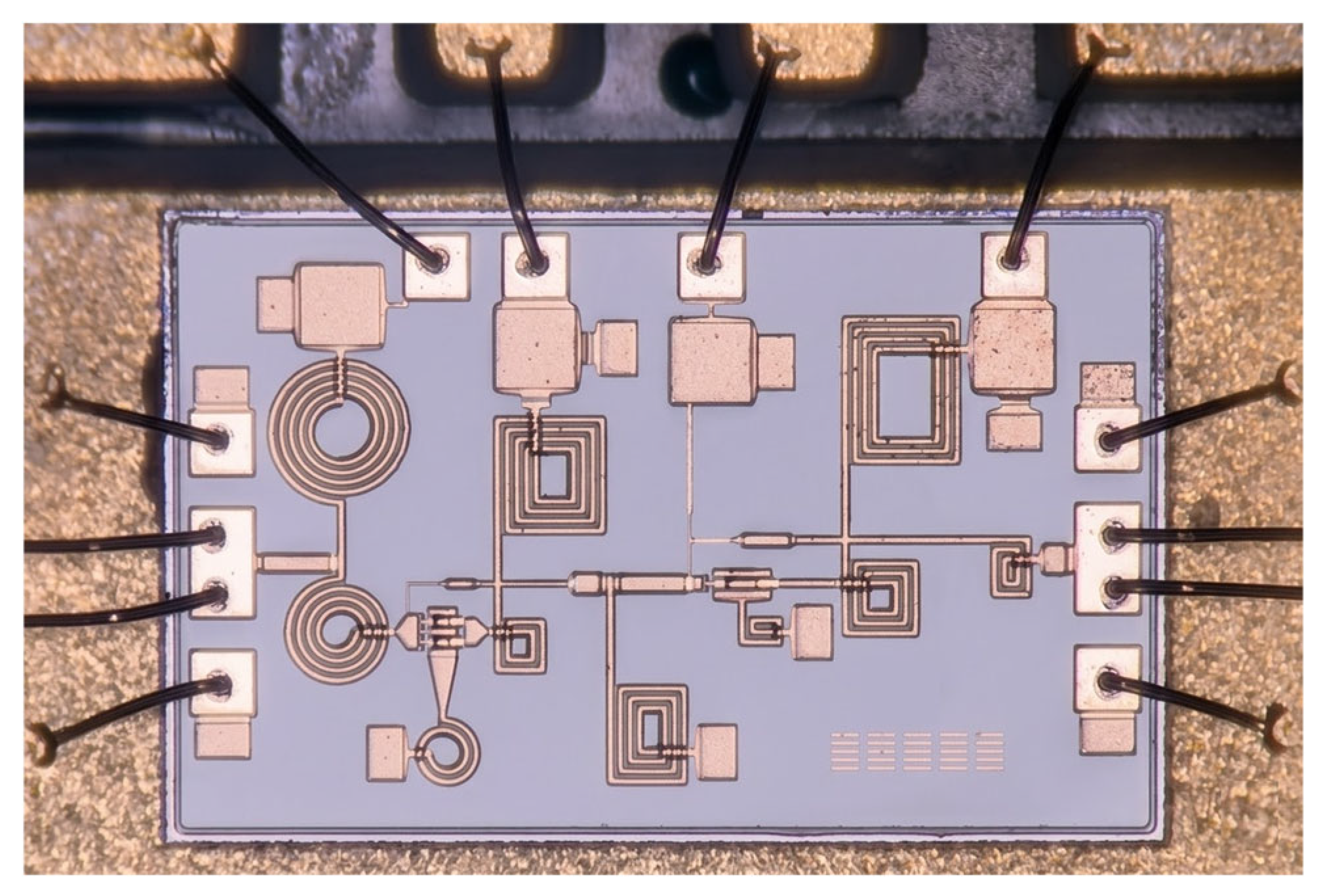
Figure 15 compares the K-factor simulation results with and without the RC feedback network. While the circuit maintains stability at higher frequencies without the feedback, the K-factor degrades in the low-frequency region due to excessive gain. The introduction of the RC feedback network effectively improves the stability by suppressing excessive gain, ensuring that the K-factor exceeds unity across the entire operating band. Figure 16 shows the chip micrograph of the proposed LNA, which occupies a compact area of 1.8 × 1.1 mm2 including the pads.

5. Results and Discussion

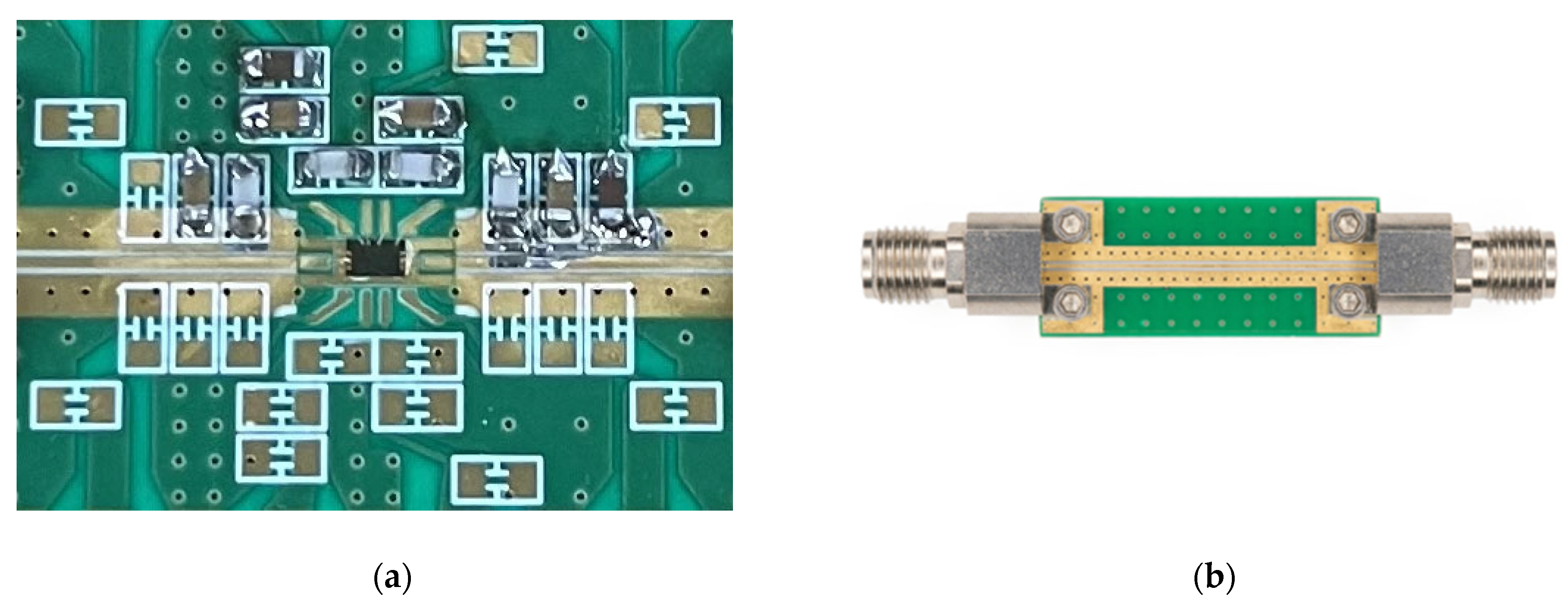
The proposed chip was fabricated using the WIN Semiconductors 0.15 µm GaAs pHEMT process. Figure 17a presents a photograph of the fabricated chip mounted on a PCB and wire-bonded. To ensure stable operation and suppress interference from the power supply lines, multiple decoupling capacitors are incorporated. In the gate bias network, where high-frequency performance is a key consideration, 100 pF and 1 nF capacitors are connected in shunt to prevent RF signal leakage. In the drain bias network, a combination of 100 pF, 1 nF, and 0.33 µF capacitors is employed in parallel to mitigate both high-frequency noise and low-frequency instability.
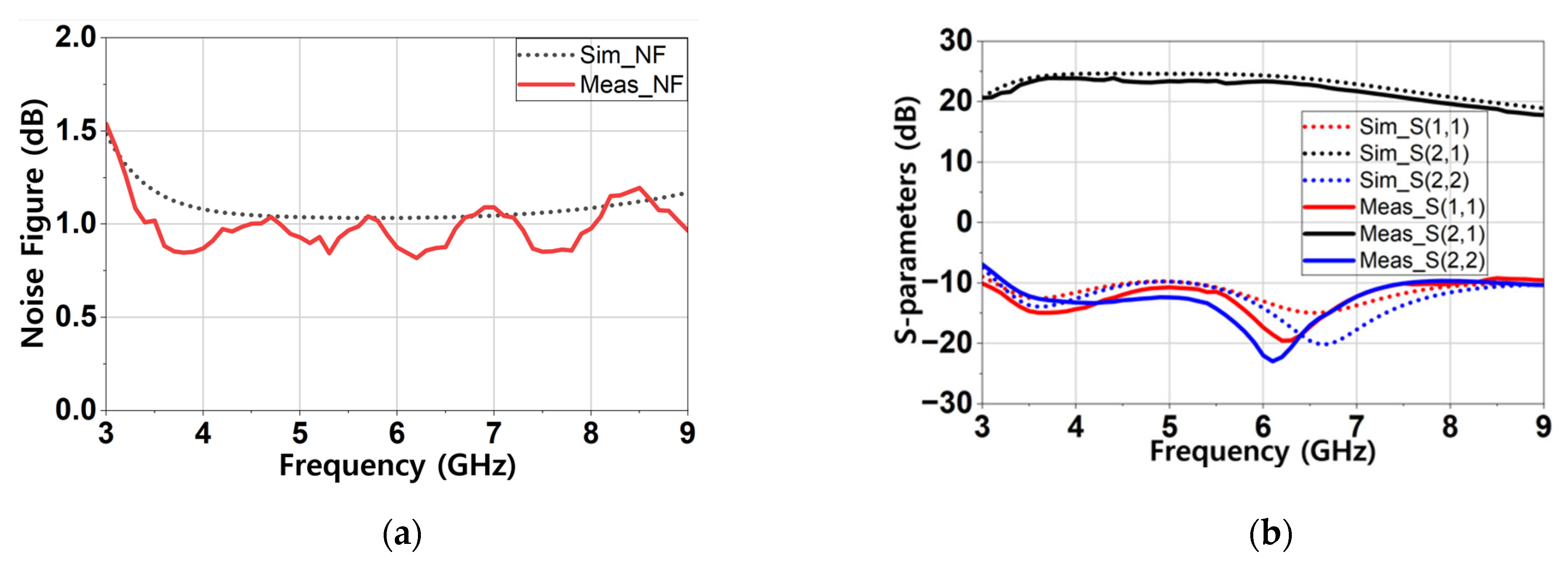
Measurements were carried out using an Agilent Technologies N8975A noise figure analyzer and an E5071C network analyzer. The proposed LNA operates at a supply voltage of 3.3 V with a gate bias of 0.35 V, resulting in a total DC power consumption of 69.3 mW. Figure 18a shows the measured NF across the 3.3–8.0 GHz band, covering portions of the S-band and C-band, with values ranging from 0.81 to 1.09 dB. The measured S-parameters are presented in Figure 18b. Over the entire frequency range, the input and output return losses remain below −10 dB and −9.7 dB, respectively. The gain exceeds 20.1 dB with a peak value of 23.9 dB, showing reasonable agreement with simulation results.
To ensure measurement reliability, a standard SOLT calibration was applied to the network analyzer to de-embed the effects of cables and connectors. The measurements were performed using K-connectors to maintain accuracy at high frequencies. The NF was measured using a calibrated noise source with a known excess noise ratio (ENR). In addition, packaging and interconnection parasitic components were taken into account during the design phase. The bond-wire inductance was modeled using two parallel wires, each having an inductance of approximately 0.5 nH, resulting in an effective inductance of about 0.3 nH when mutual coupling is considered.
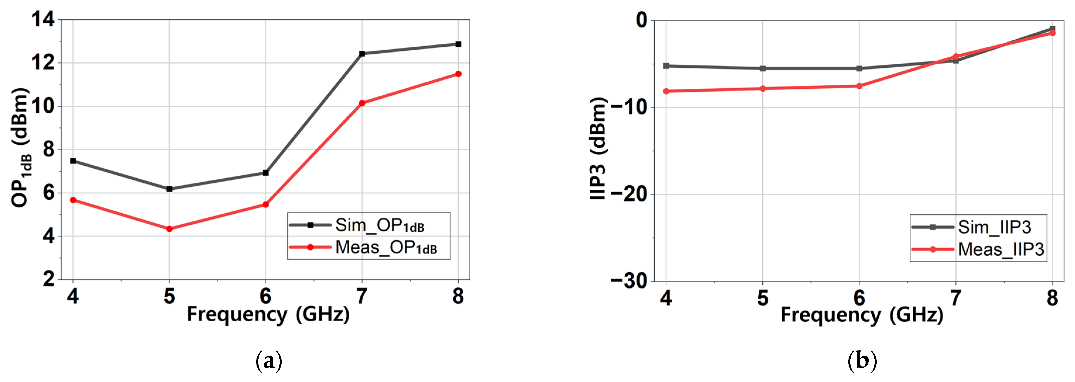
The PCB loss was characterized using a through pattern, as shown in Figure 17b, which was used to extract the PCB transmission loss. The measured loss ranges from approximately 0.43 dB at 3.3 GHz to 0.87 dB at 8 GHz, exhibiting a frequency-dependent behavior. During noise de-embedding, half of the PCB loss was subtracted to account for the input-side attenuation. Furthermore, Figure 19a presents the measured output 1-dB compression point (OP1dB), which ranges from 4.4 to 11.5 dBm across the operating band. Figure 19b shows the measured input third-order intercept point (IIP3), with an average value of −5.7 dBm.
F o M = 20 l o g 10 G a i n a b s · B W 3 d B G H z ( N F min abs 1 ) · P d c m W
To provide a comprehensive evaluation, a figure-of-merit (FoM) defined in (8) was employed, where the notation ‘abs’ denotes the absolute linear scale rather than decibels (dB). The proposed design achieved a highly competitive FoM among the reported works, demonstrating its well-balanced overall performance. In particular, the results demonstrate that the proposed LNA achieved a competitive NF with reduced power consumption compared to other GaAs-based designs. Although several recently reported state-of-the-art works employ similar inductive degeneration and feedback topologies, the proposed design differentiates itself through a detailed analytical approach to voltage gain and output impedance optimization. Specifically, high-Q circular inductors are selectively employed in the first stage to improve wideband performance while maintaining low-noise characteristics. Based on the theoretical analysis of gain and impedance behavior, the proposed design achieves a balanced trade-off among noise performance, linearity, and stability. As a result, the proposed LNA achieves a remarkably low NF of 0.81–1.09 dB while maintaining highly competitive overall RF performance. While CMOS implementations generally offer advantages in terms of low power consumption and compact chip area, GaAs technology can provide favorable RF characteristics, particularly for low-noise and high-frequency applications, due to its intrinsic material properties. Specifically, the higher electron mobility of GaAs enables increased transconductance, which can contribute to improved noise performance when properly matched. In addition, the semi-insulating substrate of GaAs enables the realization of high Q-factor passive components by minimizing substrate-induced losses, which are more pronounced in CMOS processes. Leveraging this advantage, the proposed architecture incorporates a high-Q circular inductor in the first stage, where the noise contribution significantly affects the overall NF. In particular, the reduced series loss of the circular inductor effectively suppresses the input-referred noise contribution, thereby improving the overall NF performance. Consequently, these intrinsic properties render GaAs technology highly compelling for high-frequency applications requiring exceptionally low-noise and robust signal integrity.
To further demonstrate the practical implications of this exceptionally low-noise performance, the system-level receiver sensitivity was evaluated based on the parameters of a commercial C-band weather radar [15]. The reference radar system specifies a minimum detectable power of −109.54 dBm over a receiver bandwidth ( Δ f ) of 1.38 MHz. Applying the NF of 0.87 dB measured at the center frequency to this identical bandwidth condition, the input-referred thermal noise floor ( N i n ) of a receiver utilizing the proposed LNA was calculated to be −111.73 dBm ( N i n = 174   d B m / H z + 10 l o g 10 ( Δ f ) + N F ) . This indicates that the proposed design provides a substantial margin of >2.1 dB over the stringent minimum detectable power requirement, confirming its high suitability and robustness for practical C-band radar front-ends.
Beyond macro-scale radar systems, the proposed LNA offers significant relative advantages for high-precision microwave sensing applications, such as wearable microwave sweat metasensors [16]. In such sensing systems, low-noise amplification is important for improving receiver sensitivity and the signal-to-noise ratio (SNR), particularly when detecting subtle transmission variations associated with physiological changes. The exceptionally low NF of 0.81–1.09 dB and wide operating bandwidth (3.3–8.0 GHz) make the proposed design well suited for broadband physiological sensing applications.
Finally, Table 2 summarizes the performance comparison with recent state-of-the-art wideband LNAs [17,18,19,20,21,22,23,24], including works employing inductive source degeneration and feedback techniques [19,21,22,23] in similar frequency ranges. Compared with these previously reported designs, the proposed LNA achieves a favorable balance between ultra-low noise performance and wideband operation. Demonstrating highly competitive overall RF performance in terms of NF, gain, linearity, stability, and FoM, the proposed architecture confirms its suitability for both high-fidelity microwave sensing systems and advanced radar applications.

6. Conclusions

In this paper, a two-stage LNA was designed and measured using 0.15 µm GaAs pHEMT technology. By employing RC feedback and inductive source degeneration techniques, wideband impedance matching and gain flatness were achieved over the 3.3–8.0 GHz frequency range. These design approaches effectively reduce the NF while enhancing overall circuit stability. In the first-stage design, circular inductors were adopted to achieve a high Q-factor. This configuration effectively reduces input-side losses and plays a key role in optimizing the overall noise performance of the system. The proposed LNA simultaneously supports C-band and a part of S-band. Owing to its low noise, high gain, and wideband characteristics, the proposed design is suitable for integrating multiple radar and communication systems into a single RF front-end.

Author Contributions

Conceptualization, S.J. and D.-H.L.; investigation, S.J., I.H.H.M. and J.L.; formal analysis, S.J.; writing—original draft preparation, S.J.; writing—review and editing, G.J. and D.-H.L.; supervision, G.J. and D.-H.L. All authors have read and agreed to the published version of the manuscript.

Funding

This work was supported by the Institute of Information & Communications Technology Planning & Evaluation (IITP) grant funded by the Korean government (MSIT) (No. RS-2024-00400864, Development of Upper-mid Band E-MIMO Base Station Antenna Beamforming Module).

Data Availability Statement

The data presented in this study are available on request from the corresponding author. The data are not publicly available due to proprietary research infrastructure and confidentiality agreements.

Conflicts of Interest

The authors declare no conflicts of interest.

References

  1. Chen, Z.; Wang, Z.; Chen, X.; Zhao, C.; Xie, F.; He, C. S-Band Doppler Wave Radar System. Remote Sens. 2017, 9, 1302. [Google Scholar] [CrossRef]
  2. Gou, Y.; Ma, Y.; Chen, H.; Yin, J. Utilization of a C-band Polarimetric Radar for Severe Rainfall Event Analysis in Complex Terrain over Eastern China. Remote Sens. 2019, 11, 22. [Google Scholar] [CrossRef]
  3. Lee, K.-W.; Lin, H.-C.; Wang, Y.-H. Enhancement-mode pseudomorphic high-electron-mobility transistor with a nanoscale oxidized GaAs gate. In Proceedings of the 2012 International Conference on Indium Phosphide and Related Materials, Santa Barbara, CA, USA, 27–30 August 2012; pp. 54–56. [Google Scholar]
  4. Niehenke, E.C. The evolution of low noise devices and amplifiers. In Proceedings of the 2012 IEEE/MTT-S International Microwave Symposium Digest, Montreal, QC, Canada, 17–22 June 2012; pp. 1–3. [Google Scholar]
  5. Yang, Z.; Wang, K.; Fan, Y.; Yan, Y.; Liang, X. Design of a GaAs-Based Ka-Band Low Noise Amplifier MMIC with Gain Flatness Enhancement. Electronics 2023, 12, 2325. [Google Scholar] [CrossRef]
  6. Kang, D.; Lee, Y.; Park, D.-W. A 17–38 GHz Cascode Low-Noise Amplifier in 150-nm GaAs Adopting Simultaneous Noise- and Input-Matched Gain Stage with Shunt-Only Input Matching. Electronics 2025, 14, 2771. [Google Scholar] [CrossRef]
  7. Shaeffer, D.K.; Lee, T.H. A 1.5-V, 1.5-GHz CMOS low noise amplifier. IEEE J. Solid-State Circuits 1997, 32, 745–759. [Google Scholar] [CrossRef]
  8. Sharma, A.; Kalra, D.; Kumar, M.; Bhatia, R. Design of CMOS low noise amplifier with inductive degeneration for navigation application. J. Electr. Eng. 2024, 75, 458–466. [Google Scholar] [CrossRef]
  9. Sabzi, M.; Medi, A. Analysis and design of multi-stage wideband LNA using simultaneously noise and impedance matching method. Microelectron. J. 2019, 86, 97–104. [Google Scholar] [CrossRef]
  10. Spasaro, M.; Zito, D. Input Integrated Matching in RF LNA with Inductive Degeneration in Low-Power Regime. In Proceedings of the 2018 25th IEEE International Conference on Electronics, Circuits and Systems (ICECS), Bordeaux, France, 9–12 December 2018; pp. 825–828. [Google Scholar]
  11. Li, S.; Zhang, T.; Fan, C. An Ultra-Wideband Low-Noise Amplifier Based on Inductor Peaking and Negative Feedback Techniques. In Proceedings of the 2025 International Conference on Microwave and Millimeter Wave Technology (ICMMT), Xi’an, China, 19–22 May 2025; pp. 1–3. [Google Scholar]
  12. Wu, C.-S.; Lin, T.-Y.; Chang, C.-H.; Wu, H.-M. 3—10 GHz Ultra-Wideband Low-Noise Amplifier Using Inductive-Series Peaking Technique with Cascode Common-Source Circuit. Wirel. Eng. Technol. 2011, 2, 257–261. [Google Scholar] [CrossRef][Green Version]
  13. HMC753LP4E: 1–11 GHz, 5 V, 55 mA GaAs Low Noise Amplifier. Available online: https://www.analog.com/media/en/technical-documentation/data-sheets/hmc753.pdf (accessed on 9 May 2026).
  14. Abounemra, A.M.E.; Helaoui, M.; Ghannouchi, F. A High Gain and High Linear 0.25 µm GaN HEMT Based Monolithic Integrated C-band Low Noise Amplifier. In Proceedings of the 2019 IEEE International Electromagnetics and Antenna Conference (IEMANTENNA), Vancouver, BC, Canada, 17–19 October 2019; pp. 016–019. [Google Scholar]
  15. Frech, M.; Hubbert, J. Monitoring the Differential Reflectivity and Receiver Calibration of the German Polarimetric Weather Radar Network. Atmos. Meas. Tech. 2020, 13, 1051–1069. [Google Scholar] [CrossRef]
  16. Wang, S.; Shen, Y.; Zheng, Y. Coplanar Hybridization of Half-Mode Magnetic Plasmonic Skyrmions: Realization and Application in a Flexible Wearable Microwave Sweat Metasensor. IEEE Trans. Microw. Theory Tech. 2025, 73, 9415–9428. [Google Scholar] [CrossRef]
  17. Huang, D.; Diao, S.; Qian, W.; Lin, F. A Resistive-Feedback LNA in 65 nm CMOS with a Gate Inductor for Bandwidth Extension. Microelectron. J. 2015, 46, 103–110. [Google Scholar] [CrossRef]
  18. Li, Y.; Li, X.; Huang, Z.; Tan, T.; Chen, D.; Cao, C. A Novel Low-Power Notch-Enhanced Active Filter for Ultrawideband Interferer Rejected LNA. IEEE Trans. Microw. Theory Tech. 2021, 69, 1684–1697. [Google Scholar] [CrossRef]
  19. Yan, X.; Zhang, J.; Luo, H.; Gao, S.; Guo, Y. A compact 1.0–12.5-GHz LNA MMIC with 1.5-dB NF Based on Multiple Resistive Feedback in 0.15-µm GaAs pHEMT Technology. IEEE Trans. Circuits Syst. I Reg. Pap. 2023, 70, 1450–1462. [Google Scholar] [CrossRef]
  20. Haykir Ergin, T.H.; Tuncel, U.; Topaloglu, S.; Ülkü, H.A. Design and Analysis of 3–12 GHz UWB Flat Gain LNA in 0.15 µm GaAs pHEMT Technology. Electronics 2025, 14, 3272. [Google Scholar] [CrossRef]
  21. Kumar, S.; Bhattacharyya, S.; Tolani, H.; Bhattacharyya, A.; Kumar, V.; Saha, C. Design of a Wideband Feedback-Stabilized C-Band MMIC Low-Noise Amplifier. In Proceedings of the 2025 IEEE Microwaves, Antennas, and Propagation Conference (MAPCON), Kochi, India, 14–18 December 2025; pp. 1–4. [Google Scholar]
  22. Fan, T.-H.; Choing, C.-C.; Wang, H. A 3.3 to 11.3 GHz Differential LNA with Slight Imbalance Active Balun in 0.15-µm GaAs pHEMT Process for Radio Astronomical Receiver. In Proceedings of the 2021 16th European Microwave Integrated Circuits Conference (EuMIC), London, UK, 3–4 April 2022; pp. 257–260. [Google Scholar]
  23. Zhang, H.; Qian, G.; Zhong, W.; Liu, C. A 3–15 GHz ultra-wideband 0.15-µm pHEMT low noise amplifier design. In Proceedings of the 2016 IEEE International Conference on Communication Systems (ICCS), Shenzhen, China, 14–16 December 2016; pp. 1–4. [Google Scholar]
  24. Cheng, Y.; Wang, J.; Zhang, T.; Chen, H.; Wang, Z.; Chen, W.; Yu, F. A 0.2-20 GHz ultra-low noise amplifier using parasitic-conscious optimization techniques. IEICE Electron. Express 2026, 23, 20260037. [Google Scholar] [CrossRef]
Figure 1. Comparison of noise figure across semiconductor process technologies [4].
Electronics 15 02259 g001
Figure 2. Simulated (a) NFmin; (b) MAG versus frequency for various transistors over the 2–20 GHz range at VDD = 3.3 V and VGS = 0.35 V.
Electronics 15 02259 g002
Figure 3. Simulated characteristics of transistors with various unit gate widths at 6 GHz (number of fingers = 4, VGS = 0.2–0.8 V): (a) NFmin and MAG; (b) drain current.
Electronics 15 02259 g003
Figure 4. Transistor layouts in CPW configuration: (a) 4 × 50 µm for the first stage; (b) 2 × 100 µm for the second stage.
Electronics 15 02259 g004
Figure 5. Schematic of the proposed LNA.
Electronics 15 02259 g005
Figure 6. Equivalent circuit of the input stage.
Electronics 15 02259 g006
Figure 7. Simulated input impedance S (1,1) on the Smith chart for various L S values.
Electronics 15 02259 g007
Figure 8. Effect of gate inductor L G on input matching and noise matching: (a) input impedance S (1,1) variation; (b) Sopt.
Electronics 15 02259 g008
Figure 9. Comparisons according to the inductor geometry: (a) Qs of inductors; (b) simulated minimum noise figure.
Electronics 15 02259 g009
Figure 10. Layout of the proposed LNA.
Electronics 15 02259 g010
Figure 11. Simulated performance as a function of the total gate width of the second stage transistor: (a) IIP3 at 6 GHz; (b) gain across the 3–9 GHz.
Electronics 15 02259 g011
Figure 12. Performance comparison for different source degeneration ( L s ) configurations: (a) NF and gain; (b) IIP3; (c) stability factor (K-factor).
Electronics 15 02259 g012
Figure 13. Simulated gain characteristics S(2,1) of the proposed LNA as a function of OMN design parameters: (a) L8; (b) L9; (c) L10; (d) C10.
Electronics 15 02259 g013
Figure 14. Simulated performance of the proposed LNA under varying temperature conditions (−40 °C, 25 °C, and 85 °C): (a) noise figure; (b) S(2,1).
Electronics 15 02259 g014
Figure 15. Simulated K-factor with and without RC feedback for stability comparison.
Electronics 15 02259 g015
Figure 16. Chip microphotograph of the proposed LNA (1.8 × 1.1 mm2).
Electronics 15 02259 g016
Figure 17. (a) Photograph of the fabricated the proposed LNA on a PCB; (b) PCB through pattern.
Electronics 15 02259 g017
Figure 18. Simulated and measured (a) NF; (b) S-parameters.
Electronics 15 02259 g018
Figure 19. Simulated and measured (a) OP1dB; (b) IIP3.
Electronics 15 02259 g019
Table 1. Simulated RF performance of transistors with different total gate widths at 6 GHz.
Transistor Size 2 × 50
(100 µm)
4 × 25
(100 µm)
2 × 100
(200 µm)
4 × 50
(200 µm)
2 × 150
(300 µm)
4 × 75
(300 µm)
NFmin (dB)0.3160.2730.3040.2620.3220.259
MAG (dB)22.75022.04323.08022.61923.17822.836
Current
Consumption (mA)
4.7985.0739.2989.56913.79014.040
Table 2. Performance comparison of LNAs.
Ref.TechnologyFreq. (GHz)NF (dB)S (1,1) (dB)Pdc (mW)OP1dB
(dBm)
Gain (dB)Gain Flatness (dB)Area (mm2)IIP3
(dBm)
K-FactorFoM
[17]65-ոm CMOS0.4–10.63.5–4.2<−11.012.0N/A10.4±0.90.076 *−3.2N/A17.53
[18]0.13 µm Bulk CMOS3.3–10.12.08–3.7<−11.510.2N/A16.1±1.750.8832.7N/A32.91
[19]0.15 µm GaAs pHEMT1.0–12.51.51–2.4<−8.087.512.823.6±1.650.75N/A>1.637.2
[20]0.15 µm GaAs pHEMT3.0–12.02.5–4.3<−10.0270.015.518.5±1.03.08.5>6.09.63
[21]0.15 µm GaAs pHEMT4.0–8.5<1.76<−11.5263.513.027.1±0.66.4N/A>2.524.87
[22]0.15 µm GaAs pHEMT3.3–11.31.4–5.0<−4.085.0N/A28.3±1.56.0N/AN/A44.47
[23]0.15 µm GaAs pHEMT3.0–15.01.5–2.6<−6.0200.010.031.0±3.52.0−12.0N/A45.25
[24]0.15 µm GaAs pHEMT0.2–20.01.29–1.86<−12.0400.017.015.6±0.61.5N/AN/A14.3
This Work0.15 µm GaAs pHEMT3.3–8.00.81–1.09<−10.069.311.523.9±1.91.98−1.4>1.438.19
* Core area only.
Disclaimer/Publisher’s Note: The statements, opinions and data contained in all publications are solely those of the individual author(s) and contributor(s) and not of MDPI and/or the editor(s). MDPI and/or the editor(s) disclaim responsibility for any injury to people or property resulting from any ideas, methods, instructions or products referred to in the content.