1. Introduction
Deep neural networks (DNNs) have achieved tremendous success in numerous tasks, such as computer vision and natural language processing, due to their exceptional feature extraction and generalization capabilities [
1,
2]. Currently, the deployment of DNN models typically follows the paradigm of “pre-training in the cloud using massive amounts of data, followed by inference acceleration on edge devices” [
3]. However, the parameter scale and computational complexity of modern neural networks are growing exponentially, posing severe challenges to the direct deployment of full-precision models on edge devices with severe power and area constraints [
4,
5]. Consequently, designing DNN hardware inference accelerators for edge scenarios that combine high computing power, high energy efficiency, and high security has become a central focus of both academia and industry [
6].
To alleviate the bottlenecks caused by massive computational loads and memory access overhead, researchers have proposed various acceleration schemes on different underlying hardware platforms. Application-Specific Integrated Circuits (ASICs) and Domain-Specific Architectures (DSAs) have achieved extremely high energy efficiency through deep hardware customization (e.g., Versa-DNN [
7], a mixed-precision NPU optimized for NAS [
8], and the UPE edge-cloud collaborative AI processor [
9]). Although these solutions offer outstanding peak performance, they suffer from extremely high system complexity, lengthy verification and fabrication cycles, and, once fixed, struggle to adapt flexibly to the rapid evolution of current DNN models (such as variable mixed-precision and unstructured sparse patterns). On the other hand, “MCU + NPU”-based heterogeneous platforms have low deployment costs but are highly prone to memory bottlenecks when handling deep DNNs [
10]. In contrast, Field-Programmable Gate Arrays (FPGAs), with their extremely high hardware-level reconfigurability and superior parallel scheduling capabilities (such as the highly efficient reconfigurable multi-core cryptographic accelerator RCA [
11] and shared exponential floating-point accelerator [
12]), have emerged as the ideal platform for balancing customized computing power with rapid iteration and development cycles. However, a review of current mainstream FPGA solutions for DNN acceleration reveals three major unresolved issues in practical deployment:
Lack of hardware-level support for secure model deployment: In sensitive application scenarios such as medical privacy and intelligent risk control, edge inference faces severe risks of low-level physical attacks and parameter tampering [
13,
14]. Pure software-based defenses typically force a choice between unacceptable latency or high-cost edge solutions. Meanwhile, most existing FPGA accelerators blindly pursue breakthroughs in computing power and energy efficiency, lacking underlying hardware-level cryptographic protection mechanisms. This results in significant risks of data leakage and tampering in offline edge scenarios.
Lack of native dataflow support for sparsity: Modern DNNs, due to their inherently overparameterized design and the widespread use of nonlinear activation functions such as ReLU, naturally contain a large number of redundant parameters and zero activation values [
15]. Existing FPGA architectures are largely confined to traditional dense matrix multiplication array designs, lacking mechanisms to dynamically detect and skip sparse zero values from a dataflow perspective. This results in severe consumption of valuable memory bandwidth and a surge in power consumption caused by a large number of invalid zero-value multiplication and addition operations [
16].
Severe imbalance in the utilization of on-chip resources: Existing FPGA solutions generally exhibit a “one-sided” phenomenon of over-reliance on on-chip DSP resources to perform large-scale matrix multiplication and addition operations [
12]. Since mainstream FPGA vendors today typically limit the input/output data interface width of DSPs to a moderate range of 18–64 bits to support wide-bit scientific computing, this makes it difficult for low-bit quantization schemes implemented in low-power embedded or edge computing scenarios to fully leverage the DSP’s computational potential. Meanwhile, the increasing prevalence of dataflow architectures has significantly reduced control logic, leading to a corresponding decline in BRAM utilization.
To simultaneously address the bottlenecks of data security risks, computational redundancy in sparse computing, and uneven hardware resource utilization in edge deployments, this paper proposes a secure and efficient FPGA-based deep neural network accelerator—SaE-FPGA (A Secure and Efficient FPGA DNN Accelerator). This work breaks the traditional resource utilization paradigm of FPGA accelerators by deeply integrating security encryption and sparsity awareness into the data flow. Its main contributions are as follows:
Hash-Bypass Processing Unit (HBPU): Deeply integrates a high-speed SHA-256 hardware hash encryption engine at the data stream input and pioneers the “hash sparse bitmap + hash bypass” mechanism. While performing low-level tamper-proof verification, it efficiently identifies sparse zeroes and duplicates that can skip redundant computations within adjacent computation cycles, achieving the first seamless integration of hardware data security verification with sparse computation identification and scheduling.
Flexible Mixed-Precision Processing Unit (FMP): Breaking the traditional limitation that BRAM is used solely for passive storage, this design dynamically reuses idle BRAM and LUT resources to perform Booth multiplication, constructing a heterogeneous computing array of DSP and BRAM-LUT resources. It supports multi-mode mapping ranging from “FP32-INT8-INT6-INT4,” enabling the full utilization of on-chip resources that were previously limited to a single application in the AI acceleration field.
Multi-Mode Reconfigurable Streaming Frame (MRSF): A sparsity-aware data routing framework has been designed. It can flexibly allocate computational tasks based on the characteristics of operators and parameter scales across different layers in deep neural networks, and coordinate data distribution between the DSP array and the BRAM-LUT computing units.
The remainder of this paper is organized as follows:
Section 2 discusses the background and motivation for mixed-precision quantization, sparse computation, and edge security;
Section 3 outlines the top-level architecture of this accelerator;
Section 4 provides an in-depth analysis of the working principles of the Hash-Bypass Processing Unit (HBPU) and hash security verification;
Section 5 details the microarchitectural design of the Flexible Mixed-Precision PE (FMP);
Section 6 introduces the Multi-mode Reconfigurable Streaming Frame (MRSF) and the end-to-end data flow built upon it;
Section 7 presents the comprehensive experimental results and performance evaluations; and, finally,
Section 8 concludes the paper.
2. Background and Motivation
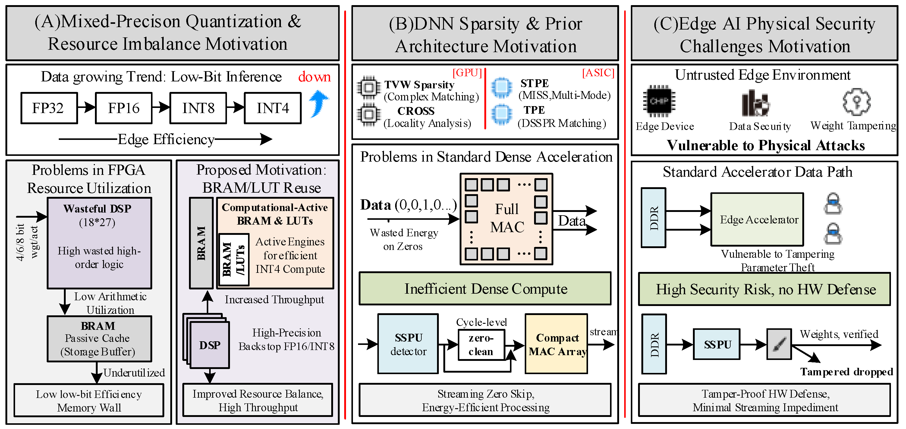
2.1. Mixed-Precision Quantization and Resource Imbalance
In the evolution of deploying modern deep neural networks to the edge, mixed-precision quantization has become a key technology for reducing model size and lowering inference power consumption [
17]. Different layers of a network often have varying sensitivity to precision, driving the evolution of inference from single FP32/FP16 to INT8, INT4, or even lower bit depths [
18].
However, traditional FPGA DNN accelerators face significant physical architecture mismatches when addressing this trend toward extremely low precision. In edge-side FPGAs based on AMD devices, the multiplier bit width of the internal DSP48E1/E2 hard cores is fixed (typically 18 × 27). When scheduling algorithms force the DSP to perform INT4 or lower-bit operations, a large number of high-order logic gates within the DSP undergo unnecessary flips, resulting in extremely low computational utilization [
19]. Although previous work has proposed frequency-doubling schemes such as DSP Packing for INT8 multiplication, they still cannot overcome the sub-50% utilization caused by the fixed bit width of the input operands in the underlying DSP architecture; In contrast, the Intel Agilex series of FPGAs integrates an Enhanced DSP with AI Tensor Block. This module is specifically optimized for machine learning and complex signal processing, capable of executing 20 INT8 multiplications per clock cycle. Compared to other FPGA architectures, this increases INT8 computational density by a factor of 5, significantly enhancing underlying hardware performance. However, the extensive BRAM resources—which serve as the core storage medium for FPGAs—are often constrained by limited bandwidth bottlenecks, leaving them idle as passive data caches. Therefore, the key motivation for improving overall system computational power lies in breaking the limitations of the traditional architecture—where “DSP dominates computation and BRAM is limited to storage”—and designing a microarchitecture capable of dynamically reusing BRAM-LUT resources to perform low-bit computations in a clock-frequency-friendly manner, as shown in
Figure 1.
2.2. Sparsity Mechanisms in DNNs and Survey of State-of-the-Art Low-Level Architectures
Modern DNNs contain massive amounts of near-zero redundant features during training and inference. Various hardware-software co-design optimization schemes have emerged to leverage this sparsity for improving computational efficiency and reducing end-to-end latency.
On GPU platforms, the core of sparsity lies in eliminating irregular memory accesses caused by unstructured sparsity. For example, addressing the challenge that dense hardware cannot efficiently handle unstructured sparsity, Guo et al. proposed the “Tile-Vector-Wide (TVW)” hybrid sparsity mechanism based on tiled matrix multiplication, which significantly reduced inference latency [
20]; Liu et al., through the end-to-end compilation framework CODA, introduced the Block Execution Timing Table (BeTT) to perform fine-grained analysis of sparse locality [
21]; additionally, incremental compression formats such as dCSR have been introduced to optimize intermediate layer representations and reduce computational overhead.
In the highly power-constrained realm of custom ASICs, model-specific low-level dataflow sparse skipping mechanisms have achieved even more significant breakthroughs in energy efficiency. The STPE processor designed by Wang et al. for edge large-model inference achieved an extremely high energy efficiency ratio under INT8 through low-level preprocessing mechanisms such as Multi-Mode Indexing and Sparsity (MISS) [
22]; the team’s earlier TPE architecture proposed Data Segment Skip and Pre-Rearrangement (DSSPR) technology, transforming high-power multiply-accumulate operations into low-power match operations [
23].
These cutting-edge works fully demonstrate that abandoning traditional global dense matrix operations and deeply integrating sparsity awareness with low-level hardware data routing and preprocessing is the only path to achieving high-efficiency acceleration. This has inspired our architecture to abandon complex offline sparse format decoding and instead design a streaming skip mechanism capable of performing zero-value pruning in real time at the clock-cycle level.
2.3. Physical Security Challenges in Edge AI
Keeping models and data at the edge for training and inference is a core requirement for breaking down data silos and protecting user privacy. However, edge devices are typically deployed in untrusted physical environments. High-value pre-trained DNN model weights and sensitive feature data face severe risks of physical tampering and parameter theft.
Existing defense mechanisms are largely confined to the software layer (e.g., fully homomorphic encryption or trusted execution environments), which introduces unacceptable performance degradation and latency overhead for edge AI chips that prioritize computational power. Although a very small number of studies (such as RCA [
11]) have explored multi-core cryptographic acceleration on FPGAs, hardware-level native cryptographic protection mechanisms are generally absent in the data paths of mainstream DNN hardware accelerators. Therefore, the core security motivation behind the design of the Hash-Bypass Processing Unit (HBPU) is to introduce low-level hardware hash verification (such as SHA-256) at the early stage when data enters the computing array to build a tamper-resistant firewall, while ensuring that high-speed data throughput is not hindered during this process.
3. SaE-FPGA Architecture
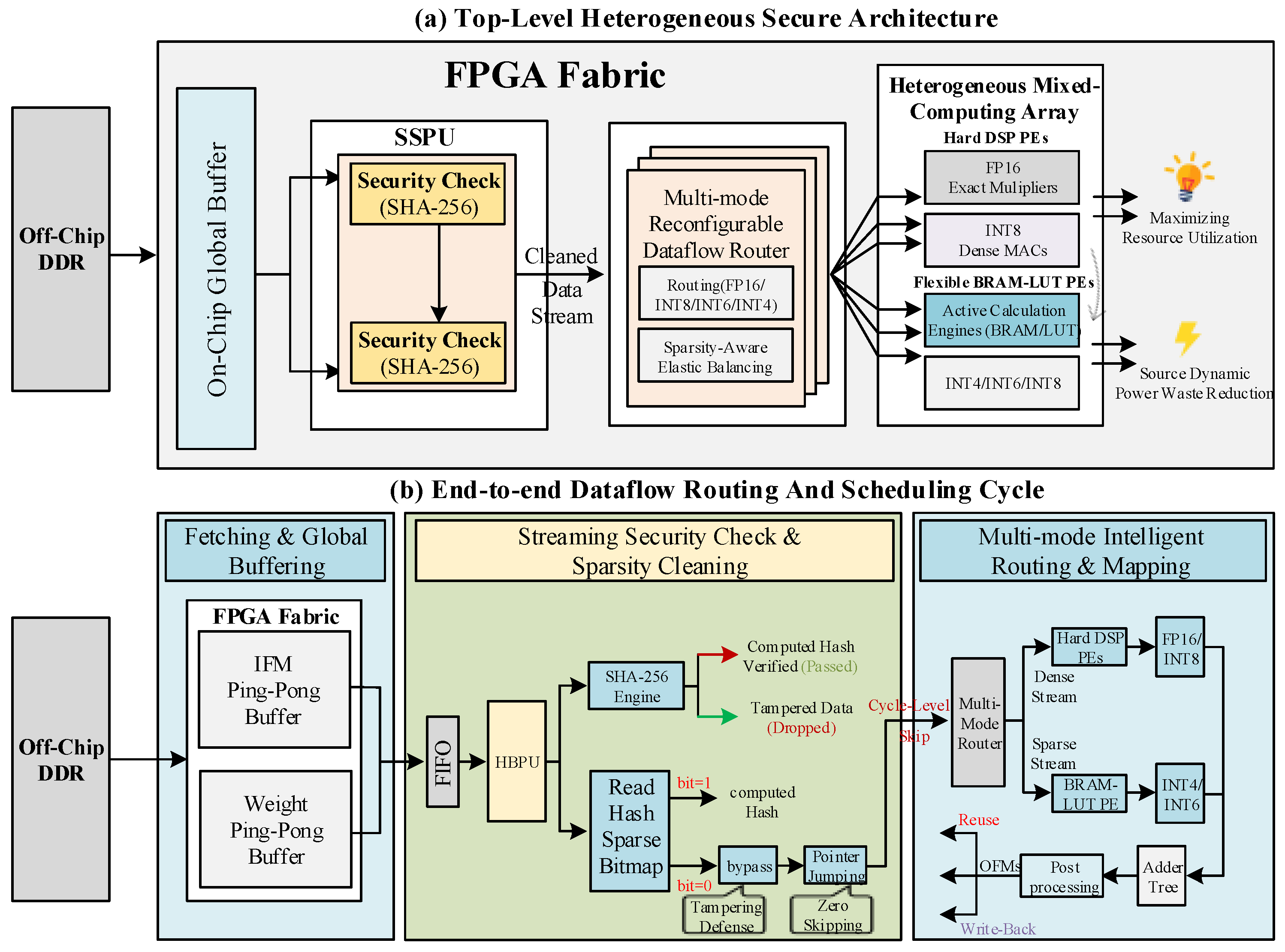
To overcome the “memory wall” bottleneck commonly found in traditional edge FPGA accelerators, as well as the severe imbalance in the utilization of computational resources (DSP and BRAM), this paper proposes a highly decoupled and deeply reused heterogeneous acceleration architecture, SaE-FPGA, and implements it on an edge FPGA. From a physical topology perspective, the system primarily consists of three core functional clusters: the Hash-Bypass Processing Unit (HBPU) located at the data input front end; the Heterogeneous Mixed-Computing Array and Multi-mode Reconfigurable Streaming Frame located in the mid-to-back end.
The data transmission method of the SaE-FPGA system differs from the strictly layered, multi-level caching architecture typified by CPUs, which relies on “computation-control-storage” separation. It abandons the traditional model where “the overall architecture depends on efficient instruction scheduling, with computing units passively waiting for stored data and control units centrally dispatching instructions.” The SaE-FPGA adopts a data-flow-oriented transmission architecture. Through fine-grained pipelining design, it avoids the waiting and backpressure issues caused by frequency mismatches between the control unit and the computing unit. The system integrates a Hash-Bypass Processing Unit (HBPU) at the start of the feature map. This unit ensures secure and trustworthy computation while utilizing the principle of skipping computations by repeatedly obtaining the same computational results. It also incorporates a DSP array and flexible mixed-precision processing units built on idle BRAM.
In actual deep neural network inference tasks, the data flow of this accelerator operates along the following paths:
Off-chip Fetching and Global Buffering: The data flow originates from off-chip DDR. Upon inference initiation, the Global Controller configures the Direct Memory Access (DMA) engine to transfer pre-trained weights and input feature maps (IFMs) to the on-chip global buffer in burst transfer mode. This buffer employs a Ping-Pong architecture to mask DDR read latency.
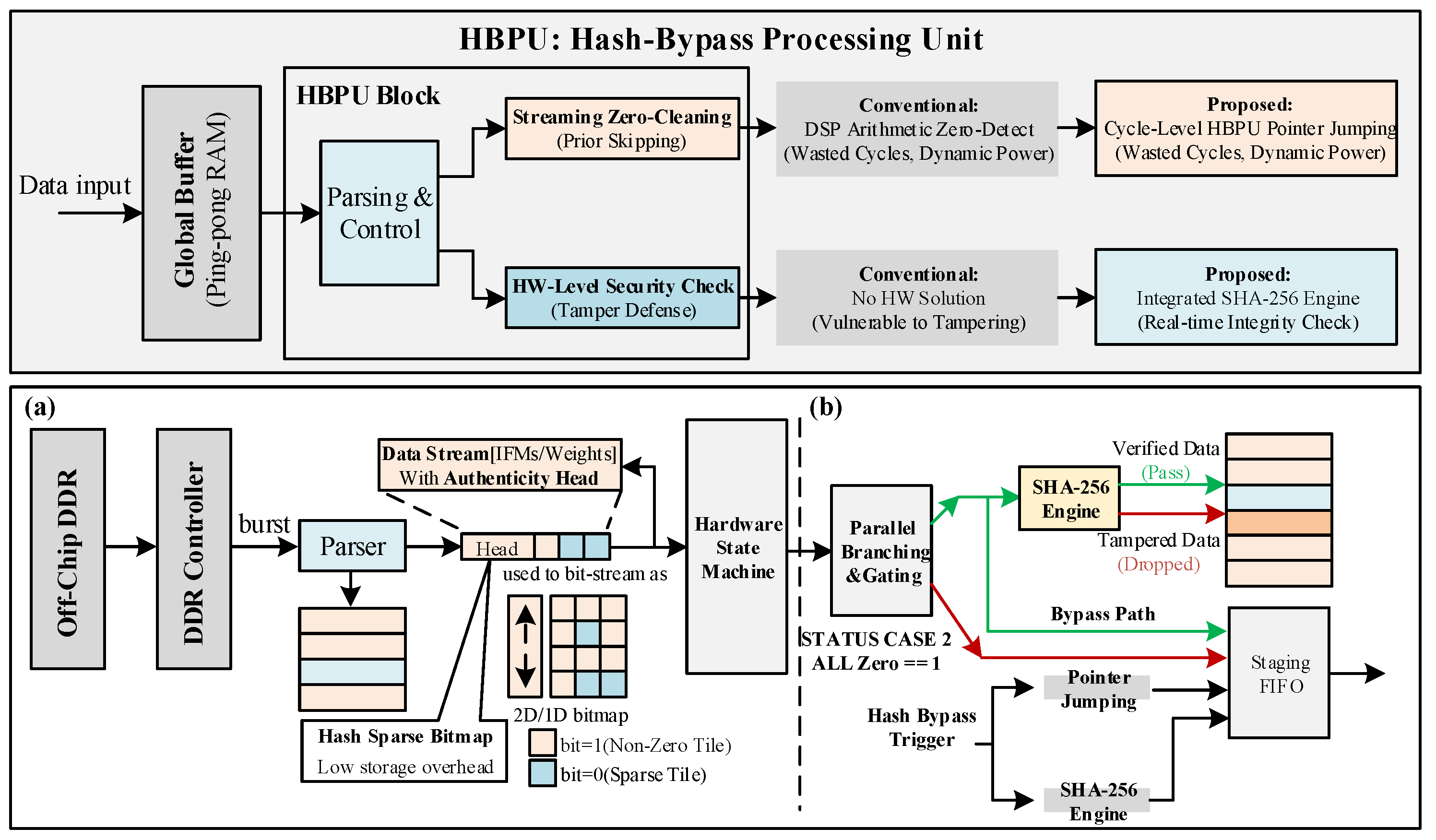
Security Check and Sparsity Filter: Before data is fed into the compute array, it undergoes hashing via a built-in high-speed SHA-256 engine, and the resulting hash value is compared against the pre-stored static weight hash results in on-chip Flash; Simultaneously, on the sparsity dimension, the parsing logic synchronously constructs a Hash Sparse Bitmap; if a partial match is found, a “Hash Bypass” is triggered, using pointer jumps to eliminate invalid data and remove invalid computation pairs from the front end.
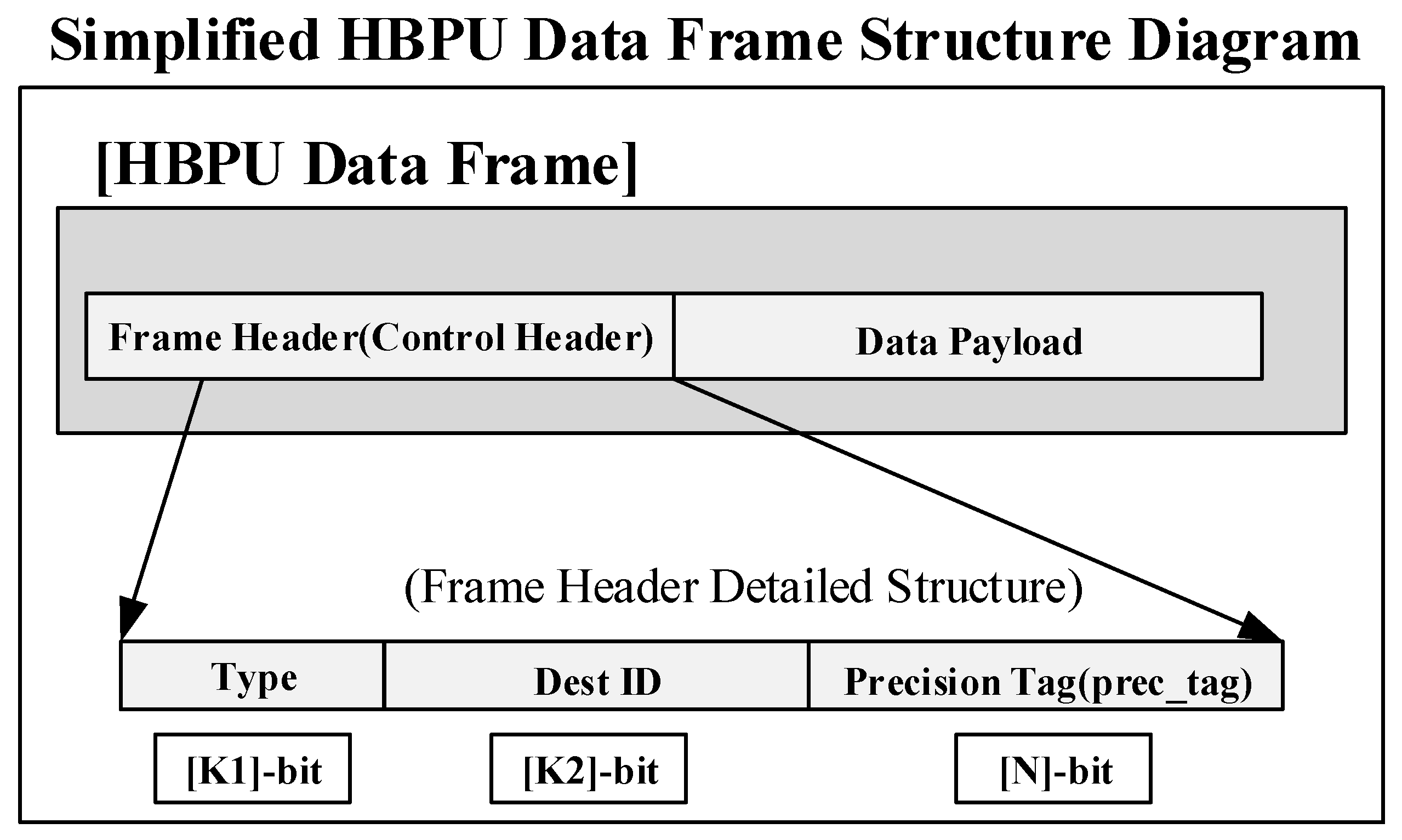
Multi-mode Routing and Mapping: Valid data streams filtered by the HBPU enter the routing network. The routing mechanism analyzes the sparsity flags in the data block control headers to perform dynamic traffic splitting: high-precision/dense data streams (such as first-layer convolutions or FP32 tasks) are directed to the hard-core DSP arrays; while low-precision data streams (such as INT4/INT8 hidden layer weights) are distributed to flexible mixed-precision PEs.
Partial Sum Reduction and Write-back: After parallel multiply-accumulate operations are completed across the heterogeneous array, partial sums are aggregated into an adder tree and accumulation buffers for channel-level reduction. They then enter the post-processing pipeline to execute activation functions (such as ReLU/GELU) and pooling. The final output feature map is written back to off-chip DDR memory via DMA.
4. Hash-Bypass Processing Unit (HBPU)
In traditional FPGA or ASIC acceleration architectures, sparse zero values in input operands continuously consume off-chip memory bandwidth and, once they enter the underlying data path, trigger a large number of unnecessary register flips, multiply-accumulate switches, and cache accesses, thereby significantly increasing the system’s dynamic power consumption. At the same time, edge deployment requires that model weights and intermediate data possess basic integrity protection capabilities before entering the compute array. To address these two requirements, SaE-FPGA has designed a Hash-Bypass Processing Unit (HBPU) at the data stream entry point to perform block-level integrity verification, sparse data filtering, and computation skipping mechanisms at the front end.
The HBPU operates at the very front end of the main data path, directly connecting the global buffer to the downstream computing array. Continuous weight streams or input feature streams from DDR must first pass through the HBPU for preprocessing and data path selection before being written to the computing array. The entire process is controlled by a state machine.
4.1. Hash Security Check Mechanism
During the offline preprocessing phase, the software writes the hash values of the current layer’s weights, derived from statistical analysis, into on-chip Flash. During the data preparation phase, the input tensor or weight tensor for each layer is divided into multiple tiles on a one-to-one basis; each tile contains a fixed number of 16 operands, each in FP32 format. The constant table (K) required for SHA-256 computation is hardcoded at startup into 16 32-bit K state registers, each with a depth of 8. After initiating the SHA-256 computation process, the HBPU performs 16-way parallel SHA-256 computations based on the parallelism of the operands within each tile, yielding a 256-bit hash value. Taking startup delay into account, the first valid result from the hash computation pipeline is synchronously compared with the precomputed hash value retrieved from the corresponding Flash address and stored in the History-RAM at the interface, and a Hash Valid signal is generated for each tile based on the comparison result. Next, the flags are sequentially stored in the Sparse Bitmap BRAM. In this BRAM, every 48 bits represent the complete information of a single tile. Thus, the hash security verification completes only half of the BRAM’s processing.
In the HBPU implementation, the hash integrity check serves as the a priori control stage of the data path. Since subsequent sparsity determination relies on the input data remaining unaltered, the hardware resource overhead imposed by the SHA-256 algorithm must be accepted. In the next state, the state machine will determine whether the current state passes the check or is discarded based on the current flag values in the Sparse Bitmap BRAM, and will output the result to the subsequent sparsity determination stage.
4.2. Zero-Skipping and Sparse Bitmap Parsing
HBPU defines a “Hash Sparse Bitmap” to describe the sparsity information of the input tensor at the tile level. Unlike traditional sparse bitmaps that only describe the distribution of non-zero elements, the Hash Sparse Bitmap is designed for security-energy efficiency co-optimization. This bitmap uses the tile as the basic management unit, packaging the hash verification results, near-zero features, and related control information for each tile. This ensures that the downstream computation array only performs memory access, register transfers, and multiply-accumulate operations on data blocks that are “verified and worth computing.”
The generation of the Hash Sparse Bitmap employs a two-stage filling mechanism. First, the upstream hash security verification module writes the index and hash validity flag to the corresponding bit of each tile. Next, the Data Parser and zero-value comparison logic complete the sparse distribution description and execution hint fields for that tile. The Data Parser first reads the key information within the tile and completes the Hash Sparse Bitmap: The 48-bit width of a single tile is divided into two parts: the lower 24 bits and the upper 24 bits. The lower 24 bits constitute the Hash Control Field, consisting of a 4-bit Tile ID, a 16-bit Hash Valid field indicating whether hash verification passed, a 1-bit Boundary Flag, and a 3-bit Layer Flag representing layer and bank information; The upper 24 bits form the Sparse Execution Field, consisting of a 16-bit Zero Mask, a 5-bit NZ Count used to count the number of non-zero elements in the current tile, a 1-bit All Zero indicator, and a 2-bit Bypass Mode flag.
After block parsing is complete, the HBPU enters the forwarding phase. This phase is carried out jointly by the state machine, the Staging FIFO, the Valid FIFO, the comparator, and the bypass control logic. The state machine reads the Hash Sparse Bitmap tile by tile in order and executes different control actions on the input data stream based on the current result.
When the state machine detects that the All Zero bit for the current tile is set to 1, it skips the entire input round. Otherwise, it performs a bitwise OR operation between the Hash Valid and Zero Mask bits. If the resulting sequence contains bits set to 1 that fail the security check or are in a sparse state, subsequent computations are discarded, and the result is set to 0. The HBPU first retrieves the valid sequence for the corresponding tile from the global buffer and sends it to the isolation staging queue. The purpose of the holding queue is to provide a controlled transition zone for summary computation, ensuring that data does not directly enter the downstream computation array before the verification result is obtained. After the verification result is confirmed, the holding queue releases the valid data. Without altering the downstream PE microarchitecture, the HBPU implements three functions: security verification based on tile-level bitmaps; sparsity assessment of retained blocks; suppressing the propagation of invalid data in subsequent stages via bypasses and address skips. Through front-end processing, the SaE-FPGA is able to maintain a streaming data transmission format while shifting data validity and integrity checks to the computation entry point. This reduces timing pressure on the mid- and back-end stages while providing a cleaner, more compact stream of valid data to the downstream heterogeneous mixed-precision arrays.
5. Flexible Mixed-Precision PE (FMP)
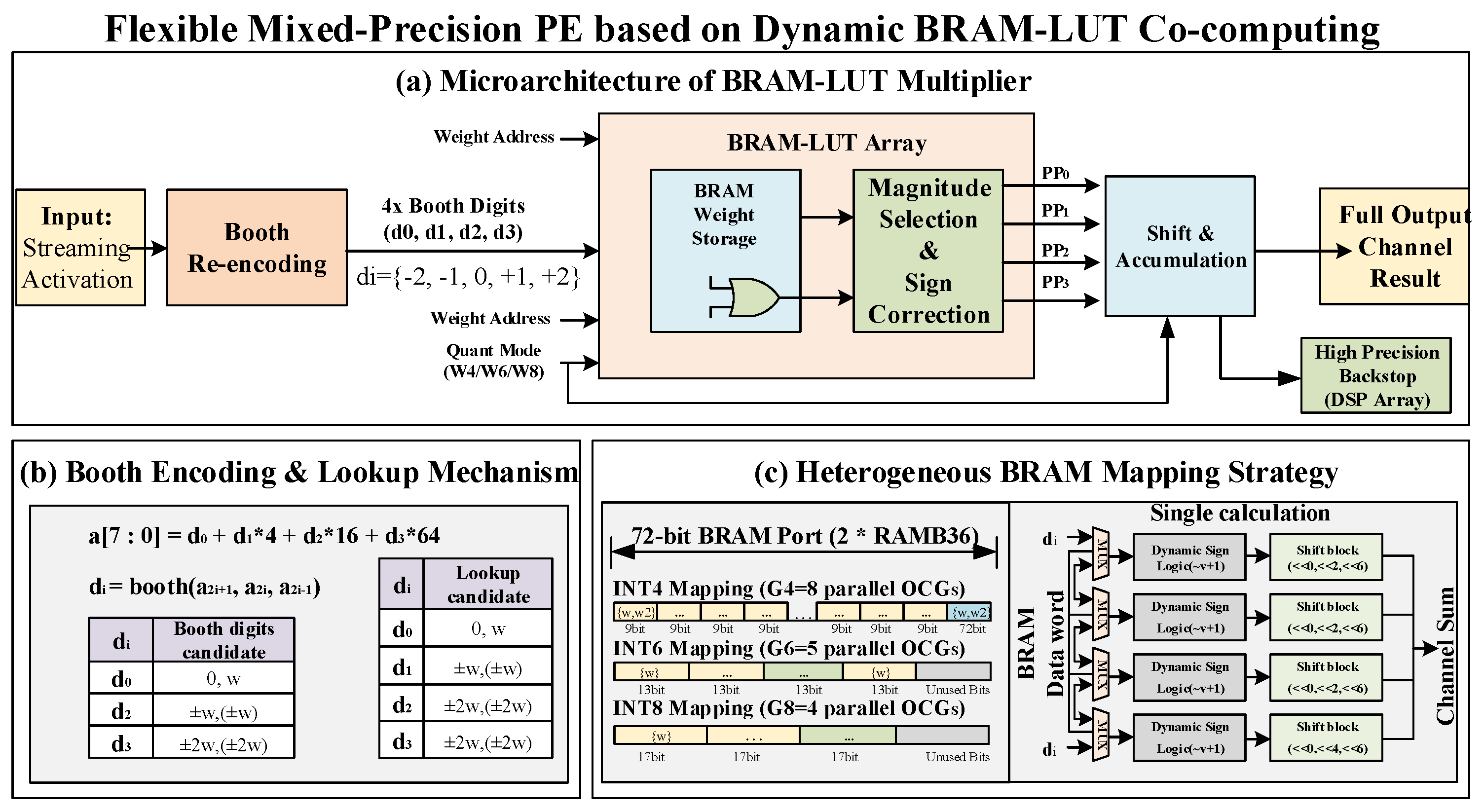
To address the excessive reliance on DSPs for quantized fixed-point operations in traditional FPGA solutions and to improve the utilization of other idle on-chip resources, this paper proposes a precision-adaptive Booth-BRAM processing unit based on the native dual-port characteristics of Xilinx BRAM. Targeting mixed-precision multiplication scenarios involving signed numbers W4/W6/W8 × A8, this unit re-encodes the streamed input activations online into a Radix-4 Booth sequence and reconstructs the multiplication operation as a combination of lookups in a small-digit magnitude vector table, sign correction, and shift-accumulation.
For FMP, a streamed sequence of signed INT8 is selected as the activation, the weight address points to the input weights, and the quant mode signal selects quantization schemes of different precisions based on operator and hierarchical characteristics. The following sections describe the Booth encoding and multiplication implementation when the activation a is signed INT8 and the weights w are signed INT4/INT6/INT8. Perform Radix-4 Booth recoding on
a [7:0]:
= booth(
,
, 0),
d1 = booth(
,
,
),
= booth(
,
,
),
= booth(
,
,
), where the encoding results
= −2, −1, 0, +1, +2, satisfying
Thus, based on Radix-4 Booth encoding, the fixed-point multiplication of weights and activations can be transformed into
The result of the 16-bit fixed-point multiplication is converted into 4 Booth partial products (Booth digits [0–3]), and since each partial product only appears in the set 0, ±w, ±2w, there is no need to store a complete product lookup table. This significantly reduces storage bandwidth and data movement overhead. To determine the sign bit of the Booth partial product, each weight is stored in the BRAM as w (w-bit two’s complement) and = w <<< 1 ((w + 1)-bit two’s complement). If the absolute value of the Booth digit is 1, w is selected; if the absolute value is 2, is selected; if the Booth digit is negative, the selected value is subjected to a two’s complement inversion and increment operation. This storage method ensures that the same four activated Booth digits correspond to the same weight word. Therefore, if a BRAM storage address already contains both wi and 2, a single read is sufficient to obtain all candidate values required for the multiplication; the four Booth digits simply select 0/±w/±2w from the same read data.
The first stage of the pipeline completes the Booth encoding, encoding the 8-bit operand into 4 Booth digits and configuring the corresponding truth table logic; the second stage organizes the weight BRAM. For each output channel group (OCG), each address stores the weight of that group of output channels at a specific reduction coordinate. The single-channel bit width is
where INT4 Bch = 9, INT6 Bch = 13, and INT8 Bch = 17. By concatenating the read data width of the BRAM using two RAMB36s, a 72-bit logical port is formed, with each physical BRAM operating in TDPx36 configuration mode. Thus, the number of parallel output channels per group is INT4 G4 = 8, INT6 G6 = 5, and INT8 G8 = 4. In this configuration, INT4 exhibits the highest parallelism, while INT8 has relatively lower parallelism. This parallelism arrangement corresponds to the computational decomposition pattern in modern DNN models, which primarily consist of shallow, small convolutions. Meanwhile, computations on the critical path can still be performed using conventional DSP arrays to ensure that the computational results meet the requirements for lossless precision.
6. Multi-Mode Reconfigurable Streaming Frame (MRSF)
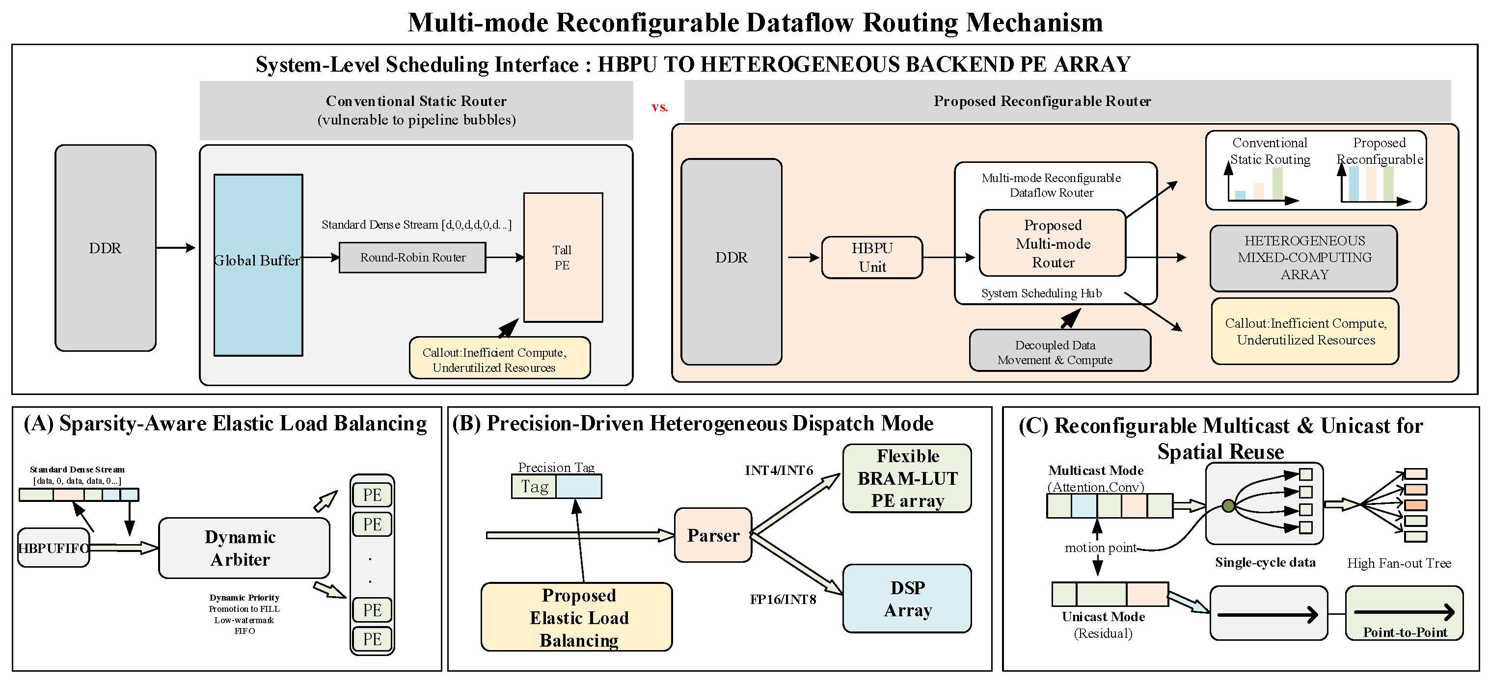
To address the severe misalignment in data distribution and bit width between the front-end Hash Bypass Processing Unit (HBPU) and the back-end heterogeneous computing array (a hybrid of hard-core DSPs and BRAM-LUT mixed-precision PEs), this paper proposes a Multi-Mode Reconfigurable Data Flow Framework (MRSF) to achieve physical-level decoupling of the front-end and back-end workflows. As shown in
Figure 5, the MRSF serves as a routing and scheduling hub, with physical interfaces consisting of input/output crossbars and configurable routing nodes. This design deeply parses the micro-instruction-level packet headers passed through the HBPU, enabling coordination between the control plane and data plane to dynamically control the multiplexing of underlying hardware data paths and task distribution. The core mechanisms of the MRSF are implemented by the following three custom hardware logic units:
6.1. Sparsity-Aware Elastic Arbitration Circuit
Since the HBPU continuously skips zero values when executing hash bypass, the data stream output to the backend exhibits highly irregular bursty traffic. If traditional static round-robin scheduling is used, the receiving PE array would remain idle due to data gaps.
To address this, MRSF instantiates asynchronous FIFO buffers with a depth of 32 at each crosspoint in the network topology, equipped with a sparsity-aware dynamic arbiter. This arbiter module receives real-time FIFO status feedback (such as almost_empty and almost_full signals) from each computational sub-array in the backend. When the arbiter detects that the FIFO water level of a specific PE group has fallen below the preset threshold 8 and its almost_empty signal goes high, the routing network’s control plane immediately uses a weighted round-robin algorithm to forcibly increase the handshake priority (grant_priority) of that data channel. This elastic load-balancing design, based on hardware state feedback, effectively absorbs time jitter caused by front-end unstructured sparsity, ensuring that the throughput saturation of the back-end heterogeneous computing array is consistently maintained at or above 90%.
6.2. Precision-Driven Heterogeneous Dispatch Logic
To accommodate mixed-precision inference in neural networks and maximize heterogeneous computing power, MRSF adopts a design that separates the data plane from the control plane, embeds a single-cycle packet parser within the routing node, and introduces precision-driven dispatch logic.
Specifically, data packets transmitted from the HBPU to the MRSF are encapsulated with a lightweight microarchitecture control header (containing an 3-bit precision tag, prec_tag; see
Figure 6). During the routing decoding phase, the packet parser within the routing node reads this tag within a single clock cycle and drives the underlying data plane multiplexer to perform precise traffic routing:
Dedicated Core (High-Precision Routing): When the prec_tag indicates high-bit-width tensors such as FP16 or INT8, the node’s control logic pulls the enable signal en_dsp_mac high and closes the transmission gate leading to the BRAM PE, directing this load-intensive data directly to the input registers of the high-speed DSP array.
Resource Decentralization (Low-Precision Routing): When prec_tag indicates low-bit-width data such as highly sparse INT4 or INT6, the resolver pulls the en_bram_pe signal high, precisely distributing the data stream to a group of flexible BRAM-LUT mixed-precision PEs for energy-efficient lookup table computations.
This traffic-splitting mechanism resolves computational mismatches at the physical layer, avoiding dynamic power waste caused by data alignment and unnecessary flips when high-bit-width MAC units process low-precision operands.
6.3. Reconfigurable Multicast and Unicast Circuits Supporting Spatial Reuse
To address the massive cache sharing demands arising from feature map reuse in deep CNNs and the multi-head attention mechanism in Transformers, MRSF supports cycle-level physical switching between unicast and multicast topologies, drastically reducing read/write bandwidth in the global cache. Based on the 1-bit mode selection mask (mode_sel_mask) issued by the MRSF configuration register, the data path can perform the following hardware reconfigurations:
Multicast Mode: When mode_sel_mask is configured as 1, the replication logic within the routing network’s crossbar is activated. A single 256-bit feature vector read from the global buffer is broadcast to 16 backend compute sub-arrays via the on-chip high-fanout tree within the same clock cycle, maximizing spatial data reuse at the physical interconnect level.
Unicast Mode: When processing compute layers without cross-channel dependencies (such as depth-separable convolutions), mode_sel_mask is set to 0. The multicast branches are clock-gated off, and the routing network degenerates into a point-to-point, directly connected FIFO data channel, providing low-latency, independent data stream transmission.
In summary, by integrating dynamic arbitration, packet-level precision routing, and topology reconfiguration techniques, MRSF effectively masks long memory access latency. With minimal additional routing overhead, it ensures computational continuity and exceptional energy efficiency for the SaE-FPGA under complex edge computing workloads.
7. Experimental Results and Performance Evaluation
7.1. Experimental Setup and Resource Utilization
This accelerator design was written in Verilog HDL and synthesized and implemented on the Xilinx Zynq 7045 platform.
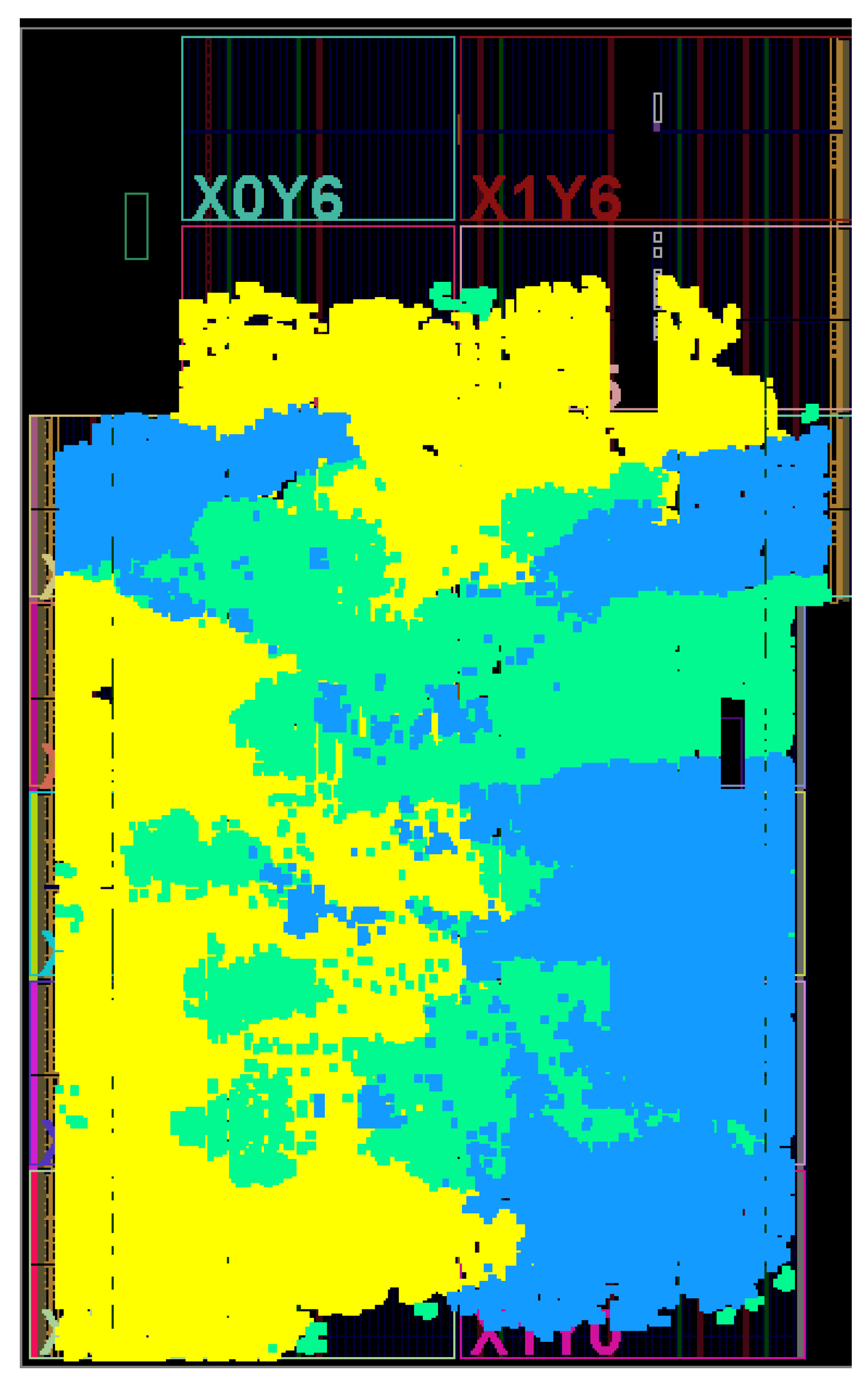
Figure 7 illustrates the physical layout. It is important to note that this specific layout visualization represents a maximal-capacity stress-test configuration. To rigorously validate the robustness of the MRSF against extreme routing congestion, we synthesized a heavily utilized configuration maximizing the on-chip global buffer allocations (capable of preserving full-batch concurrent activations: Batch Size = 4). Due to ultra-dense resource packing, this specific stress-test bitstream establishes stable timing closure at 100 MHz. However, for the primary edge-inference deployments and all the 200 MHz performance benchmarks reported in this paper, an edge-optimized configuration is utilized. By scaling the buffer parameters to target single-frame streaming (Batch Size = 1)—which aligns with the strict ultra-low latency requirements of edge applications—the routing pressure is significantly alleviated, allowing the architecture to comfortably achieve complete timing closure at the 200 MHz target frequency without severe congestion.
As shown in
Table 1, after deeply integrating the HBPU with the flexible mixed-precision PE array, the entire architecture consumed a total of 158,894 LUTs, 682 BRAMs, and 618 DSP slices. Since a significant portion of the computations that originally relied on the DSP were seamlessly offloaded to the BRAM-LUT Booth multiplier units, the DSP utilization rate in this design is only 68.6%, successfully addressing the challenge of resource imbalance in traditional FPGA solutions.
7.2. Accuracy and Throughput Evaluation
To verify the superior performance of this architecture under the mixed-precision quantization mechanism, we conducted tests on the AlexNet, ResNet-18, ResNet-34, and ResNet-50 models. We quantized FP32 to INT8/INT6/INT4 precision using LOG2 quantization and performed end-to-end performance evaluations on the Cityscapes dataset.
Accuracy Performance: As shown in
Table 2, tests were conducted on the FC/Conv layers of AlexNet, ResNet-18, ResNet-34, and ResNet-50, respectively. When the system was configured to use FP32 precision globally, the baseline accuracy rates of the models were 55.85%, 68.10%, 73.48%, and 76.70%, respectively; whereas after enabling Flexible Mixed-Precision with LOG2 quantization, the accuracy rates were 55.20%, 67.18%, 72.70%, and 76.02%, respectively. The accuracy loss was strictly controlled within 1%. This tight error boundary is achieved because LOG2 quantization strategy effectively preserves the weight distributions of sensitive layers, while the DSP array serves as a high-precision backstop for critical path computations. Furthermore, five independent repeated inference experiments were conducted on ResNet-18, yielding an accuracy fluctuation variance of only 0.91%, which further verifies the stability of the proposed mixed-precision execution scheme.
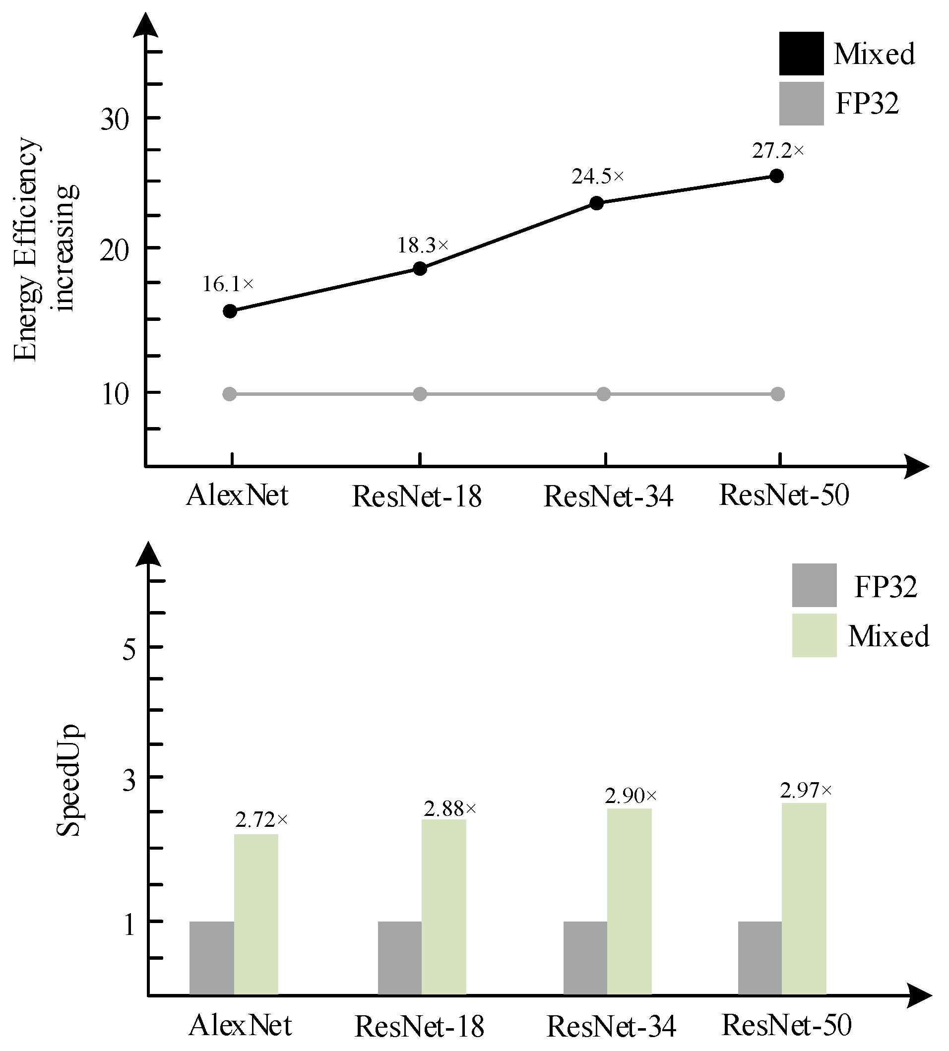
Energy Efficiency and Peak Performance: Leveraging the front-end HBPU’s streaming skipping of redundant zeros and the nearly doubled throughput provided by the back-end INT4/INT6/INT8 mixed-precision, the overall energy efficiency improved by 16.1×, 18.3×, 24.5×, and 24.5×, respectively, when the system ran at full speed in mixed-precision mode on AlexNet, ResNet-18, ResNet-34, and ResNet-50, with improvements of 16.1×, 18.3×, 24.5×, and 27.2×, respectively, under secure and trustworthy computing conditions; even higher improvements can be achieved when memory access power consumption is factored in. The acceleration ratios reached 2.72×, 2.88×, 2.90×, and 2.97×, respectively. The specific improvements in computational energy efficiency and acceleration ratios are shown in
Figure 8.
Reliability Verification: By configuring four sets of 64 random input weight and activation data pairs each with FP32/INT8/INT6/INT4 precision in the test environment. To ensure consistency between the hardware implementation and the theoretical design, a C-model verification platform was established that is fully equivalent to the SHA-256 hash computation engine. This platform strictly replicates its core hardware logic, namely the HBPU’s hash value computation and security verification processes. Comparison of software and hardware simulation results showed an error rate of less than 1%.
7.3. Security Overhead and Evaluation
Due to their highly non-linear nature, DNNs are vulnerable to microscopic parameter perturbations, where a single bit-flip can induce silent yet catastrophic misclassifications. In untrusted edge environments, physical memory is highly vulnerable to Targeted Bit-Flip Attacks (BFA) (e.g., via Rowhammer), where adversaries precisely alter critical weight bits to hijack model outputs without retraining. Recent studies reveal that flipping merely 27 out of 88 million parameters in ResNet-18 can achieve a 100% Attack Success Rate (ASR).
While lightweight error-detection schemes like standard CRC-32 require minimal hardware overhead, they are strictly linear:
allowing attackers to effortlessly compute compensatory non-critical bit-flips to force a deterministic collision and completely bypass verification. Upgrading to a Keyed-CRC (MAC-CRC) introduces complex key management vulnerabilities at the edge, whereas implementing robust cryptographic verification (e.g., SHA-256) purely in software on a host CPU creates a severe “Memory Wall,” stalling the dataflow pipeline with massive latency cycles and starving the downstream compute arrays.
To address these vulnerabilities, the proposed Hash-Bypass Processing Unit (HBPU) integrates a high-speed SHA-256 engine directly at the streaming ingress, achieving a balance between security and performance. While consuming a moderate allocation of LUTs, the hardware SHA-256 provides strong cryptographic integrity protection with a strict avalanche effect, successfully dropping the BFA Attack Success Rate to nearly 0%. Crucially, by deeply coupling the verification logic with a global Ping-Pong buffering and sparse-bypass mechanism, the computation and verification operate in a cycle-level pipeline. This architectural co-design seamlessly masks the verification latency, ensuring that the backend heterogeneous BRAM-LUT and DSP arrays maintain near-peak throughput saturation without being hindered by security overheads.
To ensure a rigorous evaluation, the end-to-end inference performance on AlexNet and the ResNet variants was measured under a strict edge-computing workload configuration. The SaE-FPGA features an instruction-driven execution model where tensor dimensions are dynamically parsed at runtime. For these experiments, the system was configured with a Batch Size of 1 running at 200 MHz. This BS = 1 configuration is intentionally selected to stress-test the memory bandwidth, representing the highly memory-bound, ultra-low latency scenarios prevalent in real-time edge streaming.
Furthermore, it is worth noting that the architecture is not physically constrained to single-frame processing. The hardware loop controllers and the Ping-Pong global buffer natively support dynamic batching. By updating the instruction configurations, the accelerator can seamlessly scale to larger batch sizes to maximize weight reuse and arithmetic intensity for multi-stream throughput-oriented tasks. Test results and comparison are summarized in
Table 3.
7.4. Comparison with the State of the Art
As shown in
Figure 8, compared to the state-of-the-art AccHashtag DNN Accelerator limited to static dense operations, our design leverages a hardware-level zero-value bypass mechanism to eliminate 23.2% of redundant computations when processing sparse features [
24,
25]. Furthermore, our architecture successfully revitalizes idle on-chip hardware resources. Under identical power constraints, it achieves a 2.97× increase in overall inference throughput and a 42% reduction in total system energy consumption, while concurrently introducing native hardware-level security protection for edge inference. Specifically, powered by the synergistic BRAM-LUT and DSP computing architecture, our accelerator delivers an outstanding throughput of 782.4 GOPS.
8. Conclusions
Based on the heterogeneous security acceleration architecture proposed in this paper, we designed and implemented a mixed-precision inference accelerator for deep neural networks using Verilog HDL. To ensure the accuracy of the evaluation, the processor was synthesized and physically implemented on the Xilinx FPGA Zynq7045 platform. This architecture deeply integrates a Hash-Bypass Processing Unit (HBPU), Flexible Mixed-Precision PEs, and a Multi-mode Reconfigurable Streaming Frame. The entire FPGA hardware system consumes a total of 158,894 LUTs, 682 BRAMs, and 618 DSP slices; through a hierarchical strategy, low-bit computations are seamlessly offloaded to BRAM-LUT Booth multiplier units, enabling the efficient utilization of idle resources to boost computational power. Ultimately, operating under this hybrid BRAM-LUT and DSP configuration, the accelerator reaches an impressive peak throughput of 782.4 GOPS.
This FPGA accelerator operates at a clock frequency of 200 MHz. When executing DNN inference tasks, thanks to the “FP32-INT8-INT6-INT4” mixed quantization mechanism, the reduction in computational and memory bandwidth achieved in mixed-precision mode results in energy efficiency improvements ranging from 16.1× to 27.2× compared to full FP32 precision. Additionally, by leveraging a hardware SHA-256 engine to verify the integrity of input data, the solution ensures trusted computing for edge deployments. The experimental results demonstrate that, compared to existing advanced FPGA acceleration solutions, the processor based on this architecture not only ensures tamper-proof security for edge data at the physical level, but also achieves nearly threefold acceleration while strictly limiting model testing accuracy loss to within 1%. This fully validates its exceptional performance in executing low-power, high-security AI inference tasks on resource-constrained edge devices.
Author Contributions
Conceptualization, Y.Z. and X.B.; Methodology, Y.Z. and J.W.; Software, Y.Z. and J.W.; Validation, Y.Z. and J.W.; Formal analysis, Y.Z.; Investigation, J.W.; Resources, Y.Z.; Data curation, Y.Z.; Writing—original draft, Y.Z. and J.W.; Writing—review & editing, X.B.; Visualization, J.W.; Supervision, X.B.; Project administration, X.B.; Funding acquisition, X.B. All authors have read and agreed to the published version of the manuscript.
Funding
This research received no external funding, the APC was funded by the authors.
Data Availability Statement
The original contributions presented in this study are included in the article. The code used in this study is not publicly available due to commercial and technical restrictions. Further inquiries can be directed to the corresponding author.
Conflicts of Interest
The authors declare no conflicts of interest, the funders had no role in the design of the study; in the collection, analyses, or interpretation of data; in the writing of the manuscript; or in the decision to publish the results.
References
- Reuther, A.; Michaleas, P.; Jones, M.; Gadepally, V.; Samsi, S.; Kepner, J. AI and ML accelerator survey and trends. In Proceedings of the 2022 IEEE High Performance Extreme Computing Conference (HPEC), Waltham, MA, USA, 19–23 September 2022; pp. 1–10. [Google Scholar]
- Silvano, C.; Ielmini, D.; Ferrandi, F.; Fiorin, L.; Curzel, S.; Benini, L.; Conti, F.; Garofalo, A.; Zambelli, C.; Calore, E.; et al. A survey on deep learning hardware accelerators for heterogeneous hpc platforms. ACM Comput. Surv. 2025, 57, 1–39. [Google Scholar] [CrossRef]
- Singh, R.; Gill, S.S. Edge AI: A survey. Internet Things Cyber-Phys. Syst. 2023, 3, 71–92. [Google Scholar] [CrossRef]
- Gholami, A.; Yao, Z.; Kim, S.; Hooper, C.; Mahoney, M.W.; Keutzer, K. Ai and memory wall. IEEE Micro 2024, 44, 33–39. [Google Scholar] [CrossRef]
- Mohaidat, T.; Khalil, K. A survey on neural network hardware accelerators. IEEE Trans. Artif. Intell. 2024, 5, 3801–3822. [Google Scholar] [CrossRef]
- Jiang, J.; Zhou, Y.; Gong, Y.; Yuan, H.; Liu, S. Fpga-based acceleration for convolutional neural networks: A comprehensive review. arXiv 2025, arXiv:2505.13461. [Google Scholar] [CrossRef]
- Yang, J.; Zheng, H.; Louri, A. Versa-dnn: A versatile architecture enabling high-performance and energy-efficient multi-dnn acceleration. IEEE Trans. Parallel Distrib. Syst. 2023, 35, 349–361. [Google Scholar] [CrossRef]
- Li, K.; Huang, H.; Huang, M.; Ding, C.; Lin, L.; Ni, L.; Yu, H. A 29.12 TOPS/W and 1.13 TOPS/mm2 NAS-optimized mixed-precision DNN accelerator with vector split-and-combination systolic in 28nm CMOS. In Proceedings of the 2024 IEEE Custom Integrated Circuits Conference (CICC), Denver, CO, USA, 21–24 April 2024; pp. 1–2. [Google Scholar]
- Wang, Z.; Du, H.; Xu, Y.; Shu, Z.; Zhou, J.; Guo, L.; Han, B.; Tang, X.; Qiao, S.; Yin, S.; et al. UPE: A Device-Edge DNN Inference Artificial Intelligence Processor with Supporting Reconfigurable Training. In Proceedings of the 2025 IEEE 7th International Conference on Artificial Intelligence Circuits and Systems (AICAS), Bordeaux, France, 28–30 April 2025; pp. 1–5. [Google Scholar]
- Zheng, H.S.; Liu, Y.Y.; Hsu, C.F.; Yeh, T.T. StreamNet: Memory-efficient streaming tiny deep learning inference on the microcontroller. Adv. Neural Inf. Process. Syst. 2023, 36, 37160–37172. [Google Scholar]
- Le, V.T.D.; Pham, H.L.; Tran, T.H.; Duong, T.S.; Nakashima, Y. High-efficiency Reconfigurable Crypto Accelerator Utilizing Innovative Resource Sharing and Parallel Processing. In Proceedings of the 2023 IEEE 16th International Symposium on Embedded Multicore/Many-Core Systems-on-Chip (MCSoC), Singapore, 18–21 December 2023; pp. 576–583. [Google Scholar]
- Zhao, W.; Dang, Q.; Xia, T.; Zhang, J.; Zheng, N.; Ren, P. Optimizing FPGA-based DNN accelerator with shared exponential floating-point format. IEEE Trans. Circuits Syst. I Regul. Pap. 2023, 70, 4478–4491. [Google Scholar] [CrossRef]
- Lim, W.Y.B.; Luong, N.C.; Hoang, D.T.; Jiao, Y.; Liang, Y.C.; Yang, Q.; Niyato, D.; Miao, C. Federated learning in mobile edge networks: A comprehensive survey. IEEE Commun. Surv. Tutor. 2020, 22, 2031–2063. [Google Scholar] [CrossRef]
- Lee, K.; Ashok, M.; Maji, S.; Agrawal, R.; Joshi, A.; Yan, M.; Emer, J.S.; Chandrakasan, A.P. Secure machine learning hardware: Challenges and progress [feature]. IEEE Circuits Syst. Mag. 2025, 25, 8–34. [Google Scholar] [CrossRef]
- Wu, Y.N.; Tsai, P.A.; Parashar, A.; Sze, V.; Emer, J.S. Sparseloop: An analytical approach to sparse tensor accelerator modeling. In Proceedings of the 55th IEEE/ACM International Symposium on Microarchitecture (MICRO), Chicago, IL, USA, 1–5 October 2022; pp. 1377–1395. [Google Scholar]
- Wu, Y. Systematic Modeling and Design of Sparse Deep Neural Network Accelerators. Ph.D. Thesis, Massachusetts Institute of Technology, Cambridge, MA, USA, 2023. [Google Scholar]
- Ou, Y.; Yu, W.H.; Un, K.F.; Chan, C.H.; Zhu, Y. A 119.64 GOPs/W FPGA-based ResNet50 mixed-precision accelerator using the dynamic DSP packing. IEEE Trans. Circuits Syst. II Express Briefs 2024, 71, 2554–2558. [Google Scholar] [CrossRef]
- Chitty-Venkata, K.T.; Somani, A.K. Neural architecture search survey: A hardware perspective. ACM Comput. Surv. 2022, 55, 1–36. [Google Scholar] [CrossRef]
- Sharma, H.; Park, J.; Suda, N.; Lai, L.; Chau, B.; Kim, J.K.; Chandra, V.; Esmaeilzadeh, H. Bit fusion: Bit-level dynamically composable architecture for accelerating deep neural networks. In Proceedings of the 45th Annual International Symposium on Computer Architecture (ISCA), Los Angeles, CA, USA, 1–6 June 2018; pp. 764–775. [Google Scholar]
- Guo, C.; Xue, F.; Leng, J.; Qiu, Y.; Guan, Y.; Cui, W.; Chen, Q.; Guo, M. Accelerating sparse DNNs based on tiled GEMM. IEEE Trans. Comput. 2024, 73, 1275–1289. [Google Scholar] [CrossRef]
- Liu, Y.; Li, W.; Zhang, K.; Liu, T.; Ye, X.; An, X. CODA: A Computation-Driven Paradigm for Sparse DNN Acceleration. IEEE Comput. Archit. Lett. 2025, 24, 381–384. [Google Scholar] [CrossRef]
- Wang, Z.; Du, H.; Mohan, V.; Zhou, J.; Shu, Z.; Xu, Y.; Han, B.; Tang, X.; Qiao, S.; Yin, S.; et al. STPE: An Energy-Efficient Edge-Device Transformer Inference Processor with Multi-Mode Data-Compression Scheme. In Proceedings of the 2025 IEEE International Symposium on Circuits and Systems (ISCAS), London, UK, 25–28 May 2025; pp. 1–5. [Google Scholar]
- Wang, Z.; Wei, J.; Tang, X.; Han, B.; He, H.; Liu, L.; Wei, S.; Yin, S. TPE: A high-performance edge-device inference with multi-level transformational mechanism. In Proceedings of the 2023 IEEE 5th International Conference on Artificial Intelligence Circuits and Systems (AICAS), Hangzhou, China, 11–13 June 2023; pp. 1–5. [Google Scholar]
- Javaheripi, M.; Chang, J.W.; Koushanfar, F. AccHashtag: Accelerated hashing for detecting fault-injection attacks on embedded neural networks. ACM J. Emerg. Technol. Comput. Syst. 2022, 19, 1–20. [Google Scholar] [CrossRef]
- Hur, S.; Na, S.; Kwon, D.; Kim, J.; Boutros, A.; Nurvitadhi, E.; Kim, J. A fast and flexible FPGA-based accelerator for natural language processing neural networks. ACM Trans. Archit. Code Optim. 2023, 20, 1–24. [Google Scholar] [CrossRef]
| Disclaimer/Publisher’s Note: The statements, opinions and data contained in all publications are solely those of the individual author(s) and contributor(s) and not of MDPI and/or the editor(s). MDPI and/or the editor(s) disclaim responsibility for any injury to people or property resulting from any ideas, methods, instructions or products referred to in the content. |