Article

Hardware–Software Co-Optimized Lightweight Real-Time CAN Intrusion Detection and Prevention System for ECUs

Department of Intelligent Semiconductors, Soongsil University, Seoul 06978, Republic of Korea
*
Author to whom correspondence should be addressed.
Electronics 2026, 15(10), 2108; https://doi.org/10.3390/electronics15102108
Submission received: 13 April 2026 / Revised: 7 May 2026 / Accepted: 13 May 2026 / Published: 14 May 2026

Abstract

The Controller Area Network (CAN) protocol used in in-vehicle networks is vulnerable to external attacks because it lacks authentication and encryption mechanisms. Accordingly, CAN Intrusion Detection Systems (IDSs) have been studied. However, existing IDSs remain difficult to deploy in practical vehicles because of their limited real-time capability, complex preprocessing, and high computational cost. To overcome these limitations, this paper proposes an ultra-lightweight Convolutional Neural Network (CNN)-based IDS that significantly reduces parameters and computational complexity while maintaining high detection performance. The proposed IDS improves area efficiency through a streaming pipeline, computation-block reuse, and constrained Processing Element (PE) parallelism. In addition, its lightweighting effect was quantitatively evaluated against an RTL baseline implemented under identical platform and design constraints. When an attack is detected, an Intrusion Prevention System (IPS) integrated with the CAN controller generates an error frame to block it in real time. The proposed IDS achieved over 99.97% detection performance for known frame-level message-injection scenarios on the Car-Hacking Dataset. It also achieved branch-wise real-time feasibility with an 11.46 µs ID-branch precomputation latency and a 5.68 µs DATA-complete-to-decision latency at 50 MHz. In TSMC 28 nm ASIC synthesis, the proposed IDS required 70,592 gates, with an estimated ASIC power of 2.0231 mW and an active inference energy of 34.68 nJ.

1. Introduction

In-vehicle networks widely use CAN for real-time control and state sharing among various Electronic Control Units (ECUs) [1]. Recently, as Vehicle-to-Everything (V2X) environments in which vehicles exchange information with external entities have become widespread, the importance of exchanging vehicle state information has increased further. This expansion of connectivity broadens the scope of in-vehicle network utilization while increasing the attack surface and thereby intensifying security threats. However, because security functions such as sender authentication and encryption were not sufficiently considered at the basic design stage, CAN is vulnerable to various attacks such as message replay and injection. These vulnerabilities can affect major vehicle functions such as steering and acceleration, potentially leading to safety accidents or casualties. Accordingly, the need for Intrusion Detection Systems that can detect and respond to attacks in real time within vehicles has been increasing [2]. Although CAN FD (Flexible Data-rate) and automotive Ethernet have been introduced to support higher-bandwidth in-vehicle communication, they have not replaced classical CAN in many ECU-level control networks. Classical CAN still represents a dominant installed base for cost-sensitive and real-time control messages because of its simple protocol structure, mature controller/transceiver ecosystem, and low integration cost. Therefore, this work focuses on a lightweight real-time IDS/IPS hardware implementation for classical CAN 2.0B extended-frame environments, rather than claiming general applicability to all in-vehicle network protocols.
Research on IDSs for in-vehicle network security has continued to advance, and, recently, deep learning-based approaches have been actively studied [3,4,5]. In addition, interest in lightweight network architectures for improving applicability to vehicular environments has also increased [6]. This is because edge devices such as automotive ECUs have severe constraints in terms of area, low power, and memory resources. Therefore, security functions operating in edge environments must be designed so that, along with high detection performance, they can be implemented within limited hardware resources. In particular, although deep learning-based IDSs can provide high accuracy, their computational and memory requirements are large; thus, hardware-friendly structural optimization is essential for actual deployment in vehicles.
The authors previously proposed the Low-Complexity IDS (LC-IDS) [7]. Although LC-IDS was presented as a software-level IDS model, it was not extended to hardware implementation and was not sufficiently lightweight in terms of computational complexity and hardware architecture for deployment in practical vehicular environments. In this paper, LC-IDS is used as the baseline model. A Co-Optimized Lightweight IDS (COL-IDS) is then proposed through joint algorithm-hardware design to reduce model complexity for efficient hardware implementation. Specifically, on the software side, the input configuration of LC-IDS is simplified to reduce the number of parameters and computational complexity, while on the hardware side, a streaming pipeline and a computation–resource–reuse architecture are employed instead of simply increasing parallelism. In addition, by constraining the PE parallelism, the architecture was designed to reduce hardware area while still satisfying the real-time requirements of CAN communication. As a result, COL-IDS reduces hardware resources and memory usage while maintaining real-time detection capability.
The contributions of this study are as follows:
  • The seven-frame Identifier (ID) sequence input of the existing LC-IDS was simplified to a single CAN ID-based architecture, and a structure capable of detection without frame buffering was proposed. Through this, input accumulation delay was eliminated, and the FLOPs were reduced from 11,242 to 4522 and the number of parameters from 4045 to 1789, achieving reductions in model complexity of approximately 59.8% and 55.8%, respectively. Nevertheless, it was experimentally verified that supervised binary detection performance comparable to that of LC-IDS was maintained for the evaluated known frame-level message-injection scenarios.
  • A streaming-pipeline datapath that partitions computation along the time dimension was designed, thereby effectively reducing hardware area without excessively expanding single-cycle parallelism. By removing the input accumulation structure, the delay characteristics were simplified, and the area-latency trade-off was adjusted to suit automotive edge environments. Through this, it was shown that real-time detection and IDS-triggered IPS operation can be supported even in resource-constrained environments.
  • The proposed IDS was implemented on FPGA and ASIC, and the benefits of each lightweighting element were quantitatively analyzed through comparison with an RTL baseline LC-IDS directly implemented under the same platform and design constraints. On this basis, the applicability of the proposed architecture to ECU-class hardware was verified in terms of resource usage, latency, chip-level gate count, estimated ASIC power, and active inference energy.

2. Related Work

CAN IDS research for in-vehicle network security has been actively conducted because the CAN protocol inherently does not provide authentication and encryption functions [2]. In particular, various deep learning-based IDSs have recently been proposed, including Deep Neural Network (DNN)-based IDS [8], CNN-based models [6,9], hybrid deep learning architectures [10], and anomaly-detection-based methods such as CANet [11] and NovelADS [12]. In addition, several survey studies show that research on deep learning-based IDSs in vehicular networks and automotive application environments continues to expand [3,4,5]. More recently, studies on lightweight network architectures for vehicular deployment have also been actively conducted [6].
However, many existing studies mainly focus on improving detection performance at the software level, and studies that jointly consider hardware resource efficiency and real-time implementability for deployment in actual ECU environments remain relatively limited [3,4,5]. In this regard, hardware-oriented studies have recently also been reported, such as Quantized Convolution Neural Network (QCNN)/Multi-Layer Perceptron (MLP)-based FPGA IDSs [13,14], Binarized Neural Network (BNN)-based FPGA IDSs [15], and ASIC-based IDS implementations [16]. Nevertheless, architectures that simultaneously satisfy model lightweighting, hardware efficiency, and real-time detection at the CAN frame level are still limited. Based on the existing LC-IDS [7], this study seeks to bridge this gap by simplifying the software architecture and applying a module-reuse-based streaming architecture suitable for FPGA and ASIC implementation.
Because prior CAN IDS studies differ in datasets, preprocessing pipelines, split protocols, detection units, and deployment assumptions, their reported software metrics are used in this work only as contextual references rather than strict head-to-head benchmarks. Similarly, prior FPGA/ASIC IDS implementations differ in FPGA devices, memory organizations, clock conditions, detection units, and latency definitions, and are therefore used as hardware-level contextual references. The controlled comparison in this paper is limited to the LC-IDS RTL baseline and the proposed COL-IDS, which were directly implemented under the same FPGA platform, fixed-point format, memory interface, clock condition, CAN-controller integration, and synthesis constraints.

3. Background

3.1. Controller Area Network

CAN is a broadcast-based serial communication protocol in which multiple nodes exchange messages over a single shared bus in automotive and industrial embedded systems. Because CAN has a multimaster structure in which multiple ECUs share the same bus, two or more nodes can begin transmission simultaneously. To resolve this, CAN uses ID-based bitwise arbitration and handles collisions nondestructively. In the CAN physical layer, a dominant bit (logic 0) overrides a recessive bit (logic 1), so each transmitting node determines whether to continue arbitration by comparing the bit it transmitted with the actual bus value. If a dominant bit is observed even though the node transmitted a recessive bit, the node is regarded as having lost arbitration and stops transmission; as a result, the message with the smaller ID is granted transmission priority. In addition, CAN provides error detection and control mechanisms such as Cyclic Redundancy Check (CRC), Acknowledgment (ACK), bit stuffing, and error frames, thereby improving communication reliability. This study targets a CAN 2.0B extended frame environment using a 29-bit ID and up to 8 bytes of DATA [1]. The targeted CAN 2.0B extended frame format is illustrated in Figure 1.

3.2. CAN Attack Types

The in-vehicle CAN bus has a structure in which multiple ECUs exchange messages in a broadcast manner, and due to design characteristics that prioritize real-time performance and simplicity, it does not provide sender authentication or encryption functions at the protocol level. Consequently, if an attacker gains access to the network, various attacks can be carried out, such as injecting messages impersonating a legitimate ECU, transmitting arbitrary data, and disrupting communication through bus occupation. In this study, DoS, Flooding, Fuzzy, Spoofing, and Malfunction attacks were considered as representative CAN attack types.
DoS and Flooding attacks are bus-occupation attacks. A DoS attack repeatedly transmits high-priority messages with low ID values, thereby occupying the CAN bus and delaying or blocking other messages. A Flooding attack similarly disrupts normal communication by injecting a large number of CAN frames within a short time. A Fuzzy attack injects messages with arbitrary IDs and DATA values into the CAN bus, generating irregular traffic patterns that differ from normal message distributions. Spoofing and Malfunction attacks are targeted message-injection attacks. A Spoofing attack impersonates a legitimate ECU by injecting messages with a specific ID, so that receiving ECUs mistake them for legitimate messages. In the Car-Hacking Dataset, Gear and RPM attacks correspond to Spoofing-type attacks. A Malfunction attack also injects crafted CAN messages intended to induce abnormal ECU or vehicle behavior. These attacks differ in their injection patterns and bus-level effects, which form the basis for IDS detection [2,17,18].

4. SW/HW Co-Optimized Lightweight IDS Model

This study aims to deploy a CAN-based IDS for automobiles in actual ECU environments. An ECU is an embedded platform with limited computational resources and memory capacity, and a detection algorithm must satisfy not only high detection performance but also low latency, stable throughput, and small model size at the same time. To this end, this study proposes a lightweight detection model that simplifies the ID input representation while maintaining the two-stream input structure of the existing LC-IDS, which consists of ID-based features and DATA-based features.
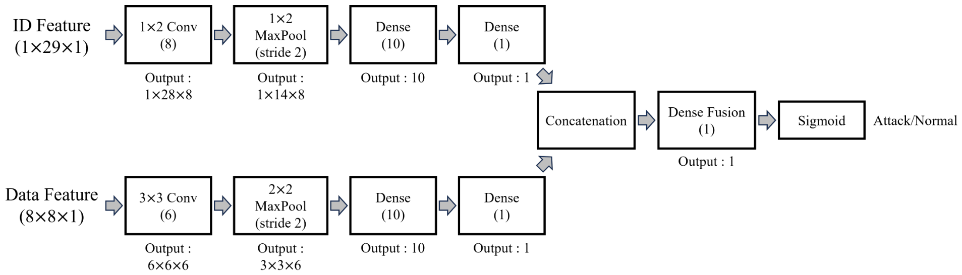
The overall architecture of the proposed model is shown in Figure 2. As in LC-IDS, the input consists of two paths, ID features and DATA features, and each path extracts features by sequentially passing through a convolution layer, a max-pooling layer, and a dense layer. Thereafter, the outputs of the two paths are combined by concatenation and finally classified as normal or attack through a dense fusion layer and a sigmoid layer [7]. The proposed model is formulated as a binary normal/attack classifier because the target IDS/IPS use case is not to diagnose the detailed attack category but to determine whether each received CAN frame should be passed or blocked in real time. The binary output directly drives the IPS trigger path, which is consistent with the lightweight hardware objective for resource-constrained ECUs.
Input features were generated on the basis of the ID and DATA of CAN 2.0B messages. LC-IDS converts the ID extracted from consecutive CAN frames into a 29-bit binary vector and arranges these vectors in temporal order to use them as a 7 × 29 ID sequence feature. In addition, the 64-bit DATA extracted from the last frame of the same window is unfolded at the bit level and formed into an 8 × 8 binary image. In this study, the DATA feature was kept the same as in the existing model, whereas only the ID feature was simplified. That is, unlike LC-IDS, which uses sequence input based on the CAN IDs of seven consecutive frames, this study constructs a 1 × 29 ID feature using only the CAN ID of a single frame. All inputs were represented only by binary values 0 and 1 without real-value conversion or normalization. Because such a single-ID-based structure does not require accumulation of past frames, it can generate a decision result as soon as the input frame arrives, which is advantageous for frame-level real-time detection and model lightweighting.
Table 1 shows a comparison of model complexity and frame-level decision characteristics between LC-IDS and the proposed architecture. By reducing the input size that must be processed in the ID branch, the proposed architecture decreases both the total computational workload and the number of parameters. Specifically, the Floating Point Operations (FLOPs) of the proposed architecture were reduced by approximately 59.8% compared with LC-IDS, and the number of parameters was reduced by approximately 55.8%. Here, FLOPs is a metric representing the amount of computation required for a single inference, and it is used to compare computational complexity and hardware implementation burden. In addition, whereas LC-IDS can perform inference only after accumulating seven consecutive frames, the proposed architecture can perform frame-level inference for each received frame without such multi-frame buffering. This removes the initial seven-frame accumulation delay required by LC-IDS and enables a frame-level decision to be generated for each received frame.
This input modification also provides direct benefits from the hardware implementation perspective. Because the sequence-based ID input of LC-IDS must internally maintain the ID information of seven consecutive frames, a frame buffer composed of shift registers as well as address and index management logic are required. By contrast, in the single-ID input architecture of this study, no accumulation buffer is required for storing seven frames of IDs, so the scale of the associated registers or memory resources and data movement logic can also be reduced. Accordingly, the storage resources and control paths for frame accumulation are reduced, which decreases area and also alleviates the waiting time and data movement overhead incurred in the input accumulation process.
Furthermore, in embedded and ASIC environments, the memory used to store model parameters accounts for a large portion of area and power consumption compared with the computation blocks themselves [19,20]. By simplifying the ID input configuration, this study reduced both the amount of computation and the number of parameters required in the ID branch. As a result, the size of Static Random Access Memory (SRAM) required to store parameters during inference is reduced, and the number of memory accesses and the volume of data movement decrease, which is also advantageous in terms of power. In addition, simplifying the ID input reduces the total amount of computation, making it possible to achieve the same throughput with fewer computational resources. This is advantageous for securing a timing margin to satisfy latency constraints in ECU environments and enables more stable operation even under worst-case conditions. Finally, the reduction in the number of parameters and computational workload relaxes the accumulation range during inference, thereby facilitating fixed-point format design and increasing the applicability of low-bit quantization.
The proposed architecture maintained supervised binary detection performance comparable to that of LC-IDS for the evaluated known frame-level message-injection scenarios. A detailed attack-wise performance comparison is presented in tabular form in the Evaluation section. These results indicate that the proposed architecture preserves detection performance after hardware-oriented lightweighting while being more suitable for ECU environments with strict latency and resource constraints.
This simplification is a hardware-oriented design choice for reducing buffering, computation, and memory requirements. However, it also introduces a detection-coverage trade-off. The proposed COL-IDS focuses on lightweight frame-level detection using the ID and DATA fields of the current CAN frame, and it does not explicitly model temporal order, message frequency, inter-arrival timing, or cross-frame context. Therefore, the proposed model should be interpreted as a lightweight frame-level IDS/IPS for known message-injection patterns represented in the training distribution, rather than as a general temporal or frequency-based CAN anomaly detector. Temporal or frequency-oriented attacks, such as exact replay attacks or frequency-only DoS patterns with legitimate-looking ID/DATA values, would require additional temporal features, such as inter-arrival timing, message-frequency modeling, or sequence-level context.

5. Hardware Implementation

5.1. Hardware Architecture Overview

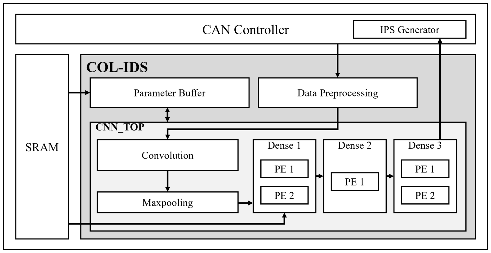
This section describes the hardware architecture and overall operational flow of the proposed COL-IDS. Figure 3 shows the overall block diagram of the COL-IDS module integrated with a CAN controller. The module receives CAN ID and DATA as inputs, generates preprocessed features, and then performs inference. Subsequently, the result of determining whether an attack is present is delivered to the IPS generator to support blocking operations against attack messages.
The architecture consists largely of SRAM, a parameter buffer, a Data Preprocessing Unit (DPU), and a CNN_TOP module. The SRAM stores the trained model parameters, and the parameter buffer temporarily stores parameters loaded from the SRAM and then forwards them to each computation module during inference, thereby reducing direct SRAM access. The DPU receives the ID and DATA from the CAN controller and generates binary features, and the generated features are input to CNN_TOP in partitioned form and sequentially processed by the internal computation modules.
Figure 3. Hardware architecture of the proposed COL-IDS integrated with a CAN controller and IPS generator.
Electronics 15 02108 g003
CNN_TOP consists of convolution, max-pooling, and three dense layers, and each computation block performs Multiply-Accumulate (MAC) operations through internal PEs. Because the ID features and DATA features in the software model architecture are processed through the same layer structure, this implementation was designed so that the two paths do not have separate hardware arranged in parallel but instead share a single computation module. Specifically, when the ID valid or DATA valid signal from the CAN controller is asserted, the corresponding input feature is streamed in, and the computation for each feature is sequentially performed under Finite-State Machine (FSM) control. The outputs of each path are combined in the fusion dense layer to generate a logit, and in hardware the decision is made on the basis of the sign of the logit without performing a sigmoid operation.
After the IDS determines the current frame to be an attack, the subsequent blocking operation is performed through the IPS path linked to the CAN controller. The IPS path can be configured through control registers. The IPS Enable signal activates or deactivates the IPS function itself. In IPS AUTO mode, the IPS generator automatically produces an error frame when the IDS classifies the current frame as an attack. In contrast, IPS RUN mode allows the processor core or a higher-level security monitor to issue a one-shot blocking command after an additional software-level decision. Therefore, the proposed IPS control structure can support monitor-only, software-supervised, and active-blocking operation modes, rather than enforcing automatic blocking in all cases.
When a blocking command is issued through the IPS path, the IPS generator outputs six consecutive dominant bits onto the bus to generate an active error flag. As a result, the attack frame currently being transmitted cannot complete normal transmission under the error-handling behavior of the CAN protocol and is processed as an error frame. Consequently, the corresponding attack message is not treated as a valid CAN frame by receiving nodes, and its propagation on the bus is blocked.

5.2. Fixed-Point Design

5.2.1. Fixed-Point Format Selection

This study applies fixed-point operations instead of floating-point operations to reduce memory usage and computational resource requirements in ECU environments. Fixed-point arithmetic is a method of representing real values using a number of bits allocated to the integer part and the fractional part, and it can reduce computational resource requirements and SRAM storage capacity for a given bit width [21]. In this case, signed fixed-point representation is used so that both positive and negative values can be expressed for parameters and intermediate computation values, and this is denoted as the Q m . n format. Here, m and n denote the number of bits for the integer part and the fractional part, respectively, and the sign bit is included separately.
The fixed-point format should be determined so as to sufficiently cover the dynamic range of values that may occur during inference. To this end, the ranges of activations in all computation blocks of the proposed model were measured, and the maximum absolute value of approximately 42.27 was observed at the output of the fusion layer. Therefore, the number of integer bits was determined so that this value could be represented without overflow, and in this study m = 6 was selected. In addition, considering hardware implementation complexity and memory efficiency, the total bit width was limited to 16 bits, and accordingly the Q 6.9 format was finally adopted. By applying this 16-bit fixed-point format, the SRAM capacity required for parameter storage can be reduced by 50% compared with 32-bit floating-point parameters. Figure 4 visually illustrates the bit composition of the selected fixed-point format.

5.2.2. PE Multiply-Accumulate in Fixed Point

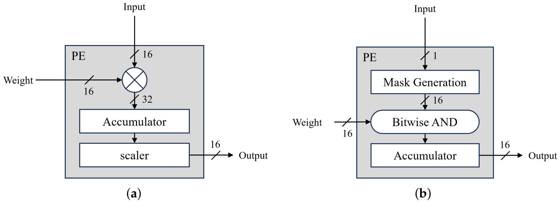
The Q6.9 fixed-point format determined in the previous subsection is used for the internal operations of the PEs in the proposed hardware. In this study, two types of PEs were designed according to the computational characteristics of each layer. Figure 5a shows the PE architecture for the dense layer, and Figure 5b shows the PE architecture for convolution operations. The two PEs maintain a consistent data representation format by unifying the inter-layer interface to 16 bits, while the internal datapaths are configured differently according to their respective computation methods.
The dense-layer PE performs MAC operations using 16-bit Q6.9-format inputs and parameters. When two Q6.9 values are multiplied, the bit width of the multiplication result is expanded, and the integer part and fractional part, excluding the sign, can increase to at most 12 bits and 18 bits, respectively. The multiplication result expanded in this way must ultimately be scale-aligned to the Q6.9 format for consistency with subsequent computation blocks. However, because the Dense layers have the largest number of accumulations in the proposed model, precision loss may accumulate if each multiplication result is immediately reduced, whereas the risk of overflow increases if the expanded values are accumulated without sufficient internal bit width. Therefore, the accumulator path in this PE was designed as 32 bits so that the expanded multiplication-result format can be maintained during accumulation. After accumulation is completed, the scaler block performs scale alignment through a right shift to adjust the number of fractional bits to the Q6.9 format, and the bit width is reduced to 16 bits through truncation for output. This approach is advantageous in terms of hardware resource efficiency because the format conversion can be implemented simply without a separate rounding circuit.
Meanwhile, the PE for convolution operations was designed as an architecture optimized for processing binary input features. This PE expands a 1-bit input into a 16-bit mask in the mask-generation block and then performs a bitwise AND operation with the parameter. Thereafter, the AND results are accumulated in the accumulator and output in a 16-bit format matching the inter-layer interface. By using a logic-operation-based datapath instead of multiplier-based computation, this approach can reduce computational complexity and hardware resource consumption in the convolution stage.
As a result, the proposed dual-PE architecture optimizes the datapath by reflecting the computational characteristics of the dense layer and the convolution layer, thereby simultaneously securing format consistency and resource efficiency in fixed-point-based inference.

5.3. SRAM Organization and Parameter Buffering

SRAM can flexibly respond to retraining or parameter updates arising from changes in data characteristics, and has the advantages of shorter latency and simpler control compared with external memory access. For these reasons, the proposed hardware was designed to store the parameters of the software model in SRAM and read them as needed during computation. However, because SRAM accounts for a large portion of the total hardware area, minimizing the required SRAM capacity is important in edge environments such as ECUs. Therefore, the software lightweighting in this study contributes not only to a reduction in computation but also to the reduction in required SRAM capacity and overall hardware resources by decreasing the amount of parameters that must be stored.
For ECU deployment, minimizing total area was set as a major design objective, and accordingly PE parallelism was limited. In particular, because Dense1 accounts for the largest share of computation due to the concentration of MAC operations for 10 output nodes, the PE parallelism was limited to two in consideration of the trade-off between area and latency. At the same time, excessively reducing parallelism may fail to satisfy the practical CAN timing margin, so the goal was to use the minimum level of parallelism that still meets the deadline. The change in latency according to the number of PEs and whether the resulting timing margin is satisfied are quantitatively analyzed in the Evaluation section. Accordingly, the SRAM width was also set to 32 bits to match a structure in which Dense1 consumes two 16-bit weights every cycle. This suppresses increases in additional buffering and control logic by preventing excessive data supply beyond the processing speed of the computation modules. In addition, a 32-bit width also matches the Advanced High-performance Bus (AHB) width, minimizing interface conversion logic and control overhead. Therefore, a 32 × 1 k SRAM (approximately 4 KB) was used as the parameter storage.
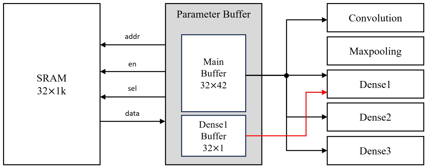
Under such limited memory interface width and restricted PE conditions, the order and method by which required parameters are supplied at each computation stage determine overall inference latency and pipeline efficiency. Therefore, this study applied differentiated supply policies in consideration of the parameter proportions and access patterns of each layer. Because Dense1 weights account for most of the total 1789 parameters, with 1660 weights, Dense1 was configured to sequentially read parameters by updating the SRAM address every cycle during inference.
However, in an environment with limited SRAM port width, it is difficult to provide the parameters of other layers immediately while SRAM access is concentrated on Dense1 weight streaming. Accordingly, an additional buffering structure may be required to supply the parameters needed at computation-stage transitions in a timely manner. Therefore, this study placed a parameter buffer between SRAM and the computation modules to decouple SRAM access from the data consumption rate of the computation stages and alleviate supply constraints. The parameter buffer reads parameters through the SRAM interface and operates as a staging buffer that distributes them to each module according to the computation stage.The proposed parameter buffer architecture is illustrated in Figure 6.
The parameter buffer consists of a 32-bit × 42-entry main buffer that stores small parameters commonly used across multiple layers and a 32-bit × 1-entry Dense1 buffer that handles continuous streaming of Dense1 weights. Small parameters required for the next stage are preloaded into the main buffer immediately after the preceding computations of each branch are completed, and during inference they are supplied to each computation module from there. As a result, the proposed parameter-buffer-based supply architecture relaxes the constraints of the streaming pipeline under limited SRAM port width and ensures stable parameter supply even during branch-transition intervals.

5.4. Streaming Pipeline

In this study, a streaming pipeline was applied to reduce hardware area instead of a layer-by-layer sequential processing scheme that stores the entire intermediate feature map. A streaming pipeline immediately transfers input data to the next computation stage as soon as it is ready, so that computation and data movement overlap along the time axis. Through this, a continuous processing flow can be maintained without large intermediate buffers, and the memory resources and area burden required for storing intermediate results can be reduced. On the other hand, the next computation stage can operate only after the minimum required input unit is secured, which requires local buffers and control logic. In addition, because data supply and stage-transition control vary according to stride and scanning order, control complexity may increase. Therefore, to fully exploit the advantages of the streaming pipeline, the design must jointly consider buffer configuration, data transfer order, and inter-stage control.
Each branch of the COL-IDS model commonly consists of one convolution layer and three dense layers. However, due to the nature of the fully connected structure, a dense layer requires the entire input vector to calculate each output node, making it difficult to apply a complete streaming pipeline across the entire region. Therefore, in this implementation, the region to which the streaming pipeline is applied was limited to DPU, convolution, max-pooling, and Dense1.
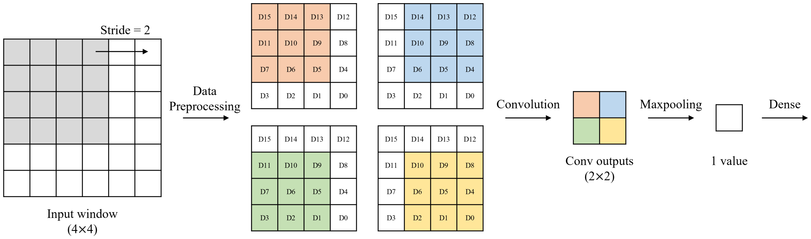
Figure 7 shows the data flow of a streaming step in the DATA branch of COL-IDS, based on 3 × 3 convolution and 2 × 2 max-pooling. One streaming step is defined as the minimum processing unit that generates one Dense1 input value and performs the corresponding Dense1 operation. For this, one max-pooling output is first required, and to obtain it a 2 × 2 convolution output feature map is needed as input. Accordingly, in one streaming step the convolution module performs four 3 × 3 convolutions in total to generate a 2 × 2 convolution output feature map. Therefore, the DPU extracts a 4 × 4 input window from the input feature map in each streaming step. As a result, one 4 × 4 input window becomes the minimum input unit for generating one Dense1 input value.
Meanwhile, because the input feature map size of the ID branch is 1 × 29 and the kernel sizes of both convolution and max-pooling are 1 × 2, it has a simpler one-dimensional streaming structure than the DATA branch. As in the DATA branch, one max-pooling output corresponds to one Dense1 input value, and for this a 1 × 2 convolution output feature is required. Accordingly, in one streaming step the convolution module performs two 1 × 2 convolutions in total to generate a 1 × 2 convolution output feature. Therefore, the DPU extracts a 1 × 3 input window from the input feature map in each streaming step.
In the proposed streaming structure, convolution operations are not performed sequentially for each kernel position; instead, the multiple convolution results required for the max-pooling input are generated together within a single step. Thus, each input feature window covers the required input range, and the next window is updated with a stride of 2 to match the max-pooling input unit.

5.5. Operation Scheduling

Figure 8 shows the operation scheduling of the proposed COL-IDS accelerator. The CLK at the top denotes the reference clock, and each lane s t e p 1 ,   s t e p 2 , ,   s t e p 54 shows the process in which the streaming steps of the DATA branch are overlapped and executed along the time axis. In this implementation, Dense1 has 10 output nodes, and because two PEs are used to process two output nodes in parallel in one cycle, the Dense1 operation for one input value requires a total of five cycles. In addition, DPU, convolution, and max-pooling were each designed to be performed in one cycle. Therefore, one streaming step consists of one cycle for DPU, one cycle for convolution, one cycle for max-pooling, and five cycles for Dense1, requiring a total of L step = 8 cycles.
As can be seen in Figure 8, adjacent streaming steps were arranged so as to overlap with the latter part of the Dense1 operation of the previous step for three cycles. This was done so that the Dense1 module, which has the largest computational workload, can operate continuously without idle cycles, and therefore the steps after the first proceed at intervals of five cycles rather than the full eight cycles. Meanwhile, the Dense1 output vector is not completed by a single step; instead, it is formed by accumulating partial sums as the step is repeated for the number of Dense1 input elements. After the Dense1 output vector is completed, the subsequent dense operations for each branch are performed sequentially. At this point, the ID branch performs only up to Dense2, whereas the DATA branch additionally performs Dense3 after Dense2. Accordingly, the final latencies for the branches can be expressed as follows:
L ID = L step , first + ( N in , ID 1 ) · L step , next + L Dense 2
L DATA = L step , first + ( N in , DATA 1 ) · L step , next + L Dense 2 + L Dense 3
Here, N in , ID and N in , DATA denote the number of Dense1 input elements in the ID branch and the DATA branch, respectively, and in this implementation N in , ID = 1 × 14 × 8 = 112 and N in , DATA = 3 × 3 × 6 = 54 . In addition, as explained earlier, L step , first and L step , next are eight and five cycles, respectively. Because Dense2 performs computation for ten inputs using a single PE, L Dense 2 = 10 cycles, and because Dense3 processes two inputs in parallel using two PEs, L Dense 3 = 1 cycle. Substituting these into the equations, the final latencies of the ID branch and the DATA branch become 573 cycles and 284 cycles, respectively.
In addition, within each streaming step, the DPU, convolution, max-pooling, and Dense1 modules were designed to be sequentially activated by control signals according to the valid timing of the output data from the previous stage. Through this, stage-wise operations are sequentially connected within a single step, while multiple streaming steps are performed in temporal overlap across the entire pipeline. As a result, the proposed operation scheduling increases the utilization of the Dense1 module while using a limited number of PEs and enables continuous inference without storing the entire intermediate feature map.

6. Evaluation

6.1. Dataset

This study performed training and evaluation using the Car-Hacking Dataset released by the Hacking and Countermeasure Research Lab (HCRL) [17]. This dataset is a public CAN intrusion dataset constructed by collecting CAN messages through the OBD-II port of an actual vehicle and conducting message-injection-based attacks. The dataset includes DoS, Fuzzy, RPM, and Gear attacks as well as normal messages, and each record consists of a timestamp, CAN ID, Data Length Code (DLC), DATA, and a flag indicating whether the record is an attack. The overall frame composition of the Car-Hacking Dataset used in this study is summarized in Table 2.
In this study, all attack types were combined into the attack class, and normal messages were defined as the normal class to train a single binary classification model. The dataset was divided into training and validation sets using a temporal-block holdout. For each attack-specific log, the records were sorted by timestamp and kept in their original temporal order. A contiguous block corresponding to the first 20% of the ordered samples was held out for validation, and the remaining 80% was used for training.
This protocol preserves temporal continuity within each split and reduces the possibility that temporally adjacent frames or samples from the same attack burst are distributed across both the training and validation sets. The early 20% block was used for validation because, in the HCRL traces used in this study, the final 20% block contained no attack-labeled frames in some attack scenarios and therefore could not form a representative validation set. The validation block was determined before model training and evaluation, and was not selected based on validation performance. The resulting training and validation composition for each attack-specific log is summarized in Table 3.
Table 2. Composition of the Car-Hacking Dataset used in this study.
Data Type# of Total Frame# of Normal Frame# of Attack Frame
DoS attack3,665,7713,078,250587,521
Fuzzy attack3,838,8603,347,013491,847
Gear attack4,443,1423,845,890597,252
RPM attack4,621,7023,966,805654,897
Table 3. Training and validation frame counts under the non-shuffled temporal-block holdout protocol.
Data TypeTrain NormalTrain AttackValidation NormalValidation Attack
DoS attack2,504,550428,066573,700159,455
Fuzzy attack2,718,003353,085629,010138,762
Gear attack3,112,269442,244733,621155,008
RPM attack3,199,611497,750767,194157,147

6.2. Evaluation Metrics

In this study, Precision, Recall, and F1-score were computed from the confusion matrix to evaluate the classification performance of the IDS. When attacks are defined as positive and normal instances as negative, true positive (TP) and true negative (TN) denote correct classification of attacks and normal instances, respectively. In contrast, false positive (FP) and false negative (FN) denote cases in which a normal instance is incorrectly judged as an attack and an attack is incorrectly judged as normal, respectively. In in-vehicle networks, FP can cause blocking of normal communication and FN can allow attacks to pass through, so both need to be minimized.
Precision reflects how many frames classified as attacks are actually attacks, and is therefore related to false-alarm suppression. Recall reflects how many actual attack frames are correctly detected, and is therefore related to missed-detection minimization. F1-score is the harmonic mean of Precision and Recall and provides a balanced indicator when both false alarms and missed detections are important. Therefore, this study used Precision, Recall, and F1-score as the main evaluation metrics.

6.3. Verification Environment

6.3.1. Software Environment

Training and evaluation of the proposed COL-IDS model were performed in a Linux environment using an AMD Ryzen Threadripper PRO 7975WX 32-Core CPU, an NVIDIA GeForce RTX 5090 GPU, 503 GiB of RAM, and the PyTorch 2.8.0+cu128 framework. During training, the batch size was set to 128, and during validation it was set to 256, and training was performed for up to 100 epochs, with early stopping applied to prevent overfitting. AdamW was used as the optimization method, the learning rate was set to 1 × 10 3 , and weight decay was set to 1 × 10 4 . In addition, a class-balanced sampler and BCEWithLogitsLoss-based pos_weight were applied to alleviate the class imbalance problem and improve training stability. During software evaluation, a logit threshold of 0, equivalent to a sigmoid threshold of 0.5, was used for the binary normal/attack decision.

6.3.2. Hardware Environment

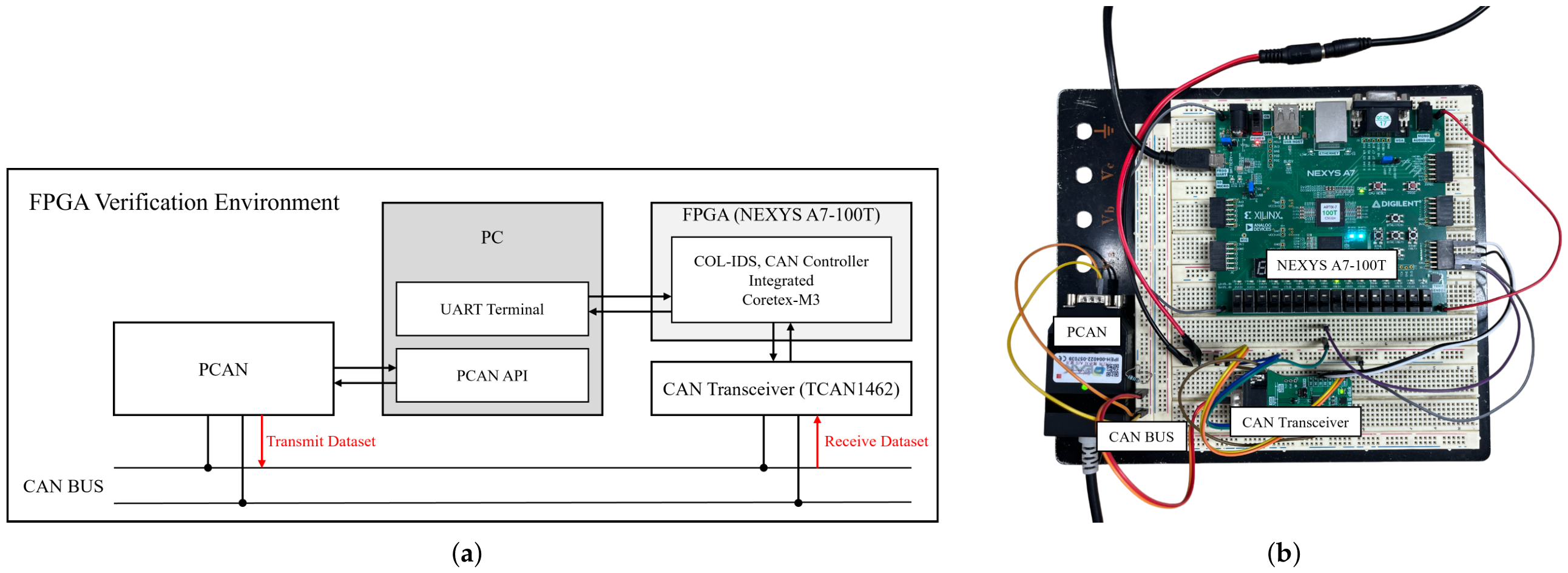
To validate the proposed hardware implementation of COL-IDS, an FPGA-based verification environment, as shown in Figure 9, was constructed. This verification environment was designed to emulate normal and attack traffic occurring in an in-vehicle CAN network and to verify the real-time inference operation of COL-IDS on FPGA. The verification environment consists of a PC, a PCAN interface, an FPGA board, and a CAN transceiver, and each device is connected through the CAN bus. In this implementation, COL-IDS was integrated with a CAN controller in a Cortex-M3-based system. This was done to reflect an actual data-processing path including AHB-based SRAM write and internal memory access, and at the same time to verify the operation of COL-IDS at a system level similar to an ECU, beyond verification at the level of a single computation block.
Figure 9a shows the block diagram of the verification environment. On the PC side, the PCAN device is controlled through the PCAN API, and CAN frames corresponding to the test dataset are transmitted over the CAN bus. The transmitted CAN frames are received through the CAN transceiver and then delivered to the COL-IDS logic inside the FPGA through the integrated CAN controller. Thereafter, COL-IDS performs real-time inference on the input frames and sends the classification results to the UART terminal on the PC through the internal UART of the core. Finally, by comparing the inference results collected through the UART terminal with the ground-truth labels, the operational correctness and detection correctness of the proposed hardware were verified. The overall verification procedure proceeded in the order of (1) transmission of test CAN frames, (2) CAN frame reception and COL-IDS inference on the FPGA, (3) result transmission through UART, and (4) comparison with ground-truth labels.
Figure 9b is a photograph of the actual hardware verification environment, which was constructed using a Nexys A7-100T FPGA board, a PCAN module, and a CAN transceiver. This shows how the block diagram of Figure 9a was realized at the actual device level and confirms that the proposed COL-IDS can operate properly in a real CAN communication environment.

6.4. Software Results

6.4.1. Car Hacking Dataset

Because the proposed model was developed by simplifying the existing LC-IDS to reduce computational complexity and model size for hardware implementation, the software-level evaluation examined whether this lightweighting affected detection performance. Table 4 reports the attack-wise Precision, Recall, and F1-score of the proposed COL-IDS together with the literature-reported reference values of existing IDS models. The DCNN, NovelADS, and HyDL-IDS values are taken from their corresponding original papers [9,10,12]. The CanNet values are included as attack-wise reference values summarized in the previous LC-IDS study [7], because the original CanNet paper [6] did not provide the same attack-wise result format for all scenarios. The LC-IDS values are also the software-side results reported in the previous LC-IDS study [7]. These values are provided as contextual references.
The attack-wise results in Table 4 do not indicate multi-class attack identification. For each known attack scenario, the model was evaluated as a binary normal/attack classifier, which is consistent with the target frame-level pass/block decision of the proposed IDS/IPS. Across the DoS, Fuzzy, Gear, and RPM scenarios, the proposed COL-IDS achieved Precision, Recall, and F1-score values of 99.9762% or higher.
Table 4. Performance of the proposed COL-IDS and the literature-reported reference values of prior IDS models.
Attack TypePerformanceDCNN [9]NovelADS [12]HyDL-IDS [10]CanNet [6]LC-IDS [7]Proposed
DoSPrecision10099.9710010099.99100
Recall99.8999.9110099.90100100
F1-score99.9599.9410099.9599.99100
FuzzyPrecision99.9599.9999.985899.8499.9999.9798
Recall99.6510099.887399.5999.9799.9762
F1-score99.8010099.936599.2199.9899.9780
GearPrecision99.9999.8910099.8510099.9987
Recall99.8999.9310099.57100100
F1-score99.9699.9110099.7110099.9994
RPMPrecision99.9999.9110099.94100100
Recall99.9499.9010099.82100100
F1-score99.9699.9110099.88100100
Note: The prior-model values are the literature-reported reference values and were not re-evaluated under identical preprocessing pipelines, split protocols, training conditions, or implementation assumptions. Therefore, this table should be interpreted as a contextual reference rather than a strict controlled head-to-head comparison.
Among the reference models, LC-IDS is the closest software-side baseline because the proposed COL-IDS was derived from LC-IDS by simplifying the ID input structure and redesigning the model for hardware-oriented implementation. The reported LC-IDS values are used as the main software-side reference for assessing performance retention. Compared with this reference, the proposed COL-IDS maintained a similar level of detection performance while reducing the input buffering requirement, FLOPs, and number of parameters. These results show that the proposed architecture preserves the detection performance of the LC-IDS-based software model while providing a more lightweight structure for FPGA/ASIC implementation.
To examine the contribution of each input field to the high validation performance, an ablation analysis was performed using three input settings: ID only, DATA only, and full ID+DATA. The corresponding feature-wise performance comparison is summarized in Table 5. The ablation results show that both ID and DATA contain effective frame-level cues for message-injection attack scenarios in the HCRL Car-Hacking Dataset. In particular, when specific injected IDs or payload patterns are repeatedly observed, many attack frames can be distinguished even using a single input field.
However, the single-branch models produced more false positives than the full ID+DATA model. This indicates that the full model can make a more stable binary normal/attack decision by using the complementary information of the ID and DATA features. Therefore, this result should be interpreted not as evidence that the proposed model detects general temporal or frequency-based CAN anomalies, but as evidence that the full ID+DATA structure is effective in reducing false positives for the evaluated known frame-level message-injection patterns while maintaining a lightweight frame-level IDS/IPS structure. Accordingly, the high validation performance for the DoS, Gear, and RPM scenarios should be interpreted as detection of known frame-level injection patterns in the evaluated HCRL traces, rather than as evidence of robustness to frequency-only DoS attacks or unseen spoofing patterns that preserve legitimate-looking ID/DATA values. Temporal or frequency-oriented attacks would require additional temporal features, such as inter-arrival timing, message-frequency modeling, or sequence-level context.
Table 5. Feature-wise performance comparison of the proposed COL-IDS on the Car-Hacking Dataset.
MetricsFeatureDoS AttackFuzzy AttackGear AttackRPM Attack
PrecisionID71.984567.596565.968765.4267
DATA90.691785.922479.091878.2647
ID & DATA10099.979899.9987100
RecallID10098.7028100100
DATA10099.9611100100
ID & DATA10099.9762100100
F1-scoreID83.710480.240479.495479.1005
DATA95.118692.411688.325487.8073
ID & DATA10099.978099.9994100

6.4.2. Survival Analysis Dataset

As a secondary software-level validation, the proposed COL-IDS was also evaluated on the HCRL Survival Analysis Dataset [18]. This dataset contains CAN traffic collected from three vehicle models, Kia Soul, Hyundai YF Sonata, and Chevrolet Spark, and includes Flooding, Fuzzy, and Malfunction attack scenarios. The same COL-IDS architecture and frame-level ID/DATA preprocessing were used without modifying the model structure. To keep the evaluation protocol consistent with the main experiment, each vehicle/attack log was sorted by timestamp and evaluated using a non-shuffled temporal-block holdout. The performance results on the second public dataset are summarized in Table 6.
These results indicate that the proposed frame-level ID/DATA architecture can also be trained and evaluated on another public CAN IDS dataset without structural modification. However, this experiment should be interpreted as a secondary dataset-level validation rather than complete deployment readiness or strict cross-vehicle generalization, because it was not designed as a train-on-one-vehicle/test-on-another-vehicle evaluation.
Table 6. Performance of the proposed COL-IDS on the second public HCRL CAN dataset.
Attack TypePerformanceKIA SoulHyundai YF
SONATA
Chevrolet
Spark
FloodingPrecision100100100
Recall100100100
F1-score100100100
FuzzyPrecision99.978999.978199.8018
Recall99.947499.890898.9780
F1-score99.963299.934499.3882
MalfunctionPrecision99.9556100100
Recall99.9556100100
F1-score99.9556100100

6.5. Hardware Results

Table 7 summarizes the frame-level and logit-level consistency between the Float32 software model and the Q6.9 FPGA implementation. The Q6.9 FPGA implementation produced the same attack-wise Precision, Recall, and F1-score values as the Float32 software model on the validation set, indicating that the fixed-point implementation did not degrade the supervised binary detection performance at the metric level.
Table 8 presents the comparison of post-synthesis FPGA resource usage between prior FPGA-based IDSs and the proposed IDS. In particular, this table also shows the resource differences between the baseline LC-IDS, which was first implemented at RTL in the same Nexys A7-100T environment, and the proposed COL-IDS architecture lightweighted on that basis. The baseline LC-IDS and the proposed COL-IDS were both directly designed and synthesized at RTL under the same platform and implementation conditions in this study. Here, the baseline LC-IDS is a hardware architecture implemented on the basis of the existing software model and was designed in a streaming manner using five PEs in the Dense1 layer. Except for the Dense1 PE count and the model-dependent input/parameter sizes, the baseline LC-IDS and the proposed COL-IDS were implemented under the same RTL design conditions, including the fixed-point format, computation modules, memory interface, and synthesis constraints. Therefore, while presenting the FPGA implementation results of the proposed architecture, this table also quantitatively shows the benefits of lightweighting over the baseline in terms of LUTs, FFs, and on-chip memory usage. The prior FPGA-based IDS results are included as contextual references because their FPGA devices, model structures, detection units, and operating assumptions differ. The primary controlled hardware comparison in this work is between the RTL LC-IDS baseline and the proposed COL-IDS implemented under the same Nexys A7-100T platform and design constraints.
Table 7. Frame-level and logit-level consistency between Float32 software and Q6.9 FPGA implementations.
MetricValue
Attack-wise Precision/Recall/F1Identical to Float32 SW
Frame-level prediction agreement100.0000%
Sign-change count0
MAE/RMSE of final logits0.01957/0.02380
95th/99th percentile absolute logit error0.04351/0.05772
Maximum absolute logit error0.11060
However, identical aggregate metrics alone do not fully guarantee that the two implementations make the same decision for every individual CAN frame. Therefore, the final pre-sigmoid logits of the Float32 software model and the Q6.9 FPGA implementation were additionally compared on a frame-by-frame basis. The Q6.9 logits were converted back to their real-valued scale before comparison, and the logit-level error was evaluated using MAE, RMSE, high-percentile absolute errors, and maximum absolute error.
As shown in Table 7, the frame-level prediction agreement between the Float32 software model and the Q6.9 FPGA implementation was 100.0000%, and no sign-change case was observed over the validation frames. Since the hardware implementation makes the binary normal/attack decision by checking the sign of the final logit, the zero sign-change count means that Q6.9 quantization and truncation did not change the final IDS decision for any validation frame. The final-logit MAE and RMSE were 0.01957 and 0.02380, respectively, and the 95th and 99th percentile absolute logit errors were 0.04351 and 0.05772, respectively. Even the maximum absolute logit error was 0.11060, and this numerical deviation did not cause any decision reversal around the logit-zero decision boundary.
These results show that the Q6.9 FPGA implementation preserves not only the aggregate Precision, Recall, and F1-score of the Float32 software model, but also the frame-level binary decisions. Therefore, the following FPGA resource, latency, timing-margin, and IPS-operation analyses are based on a fixed-point implementation that maintains the validation behavior of the original Float32 software model.
Table 8. FPGA resource results of the proposed COL-IDS, the timing-feasible LC-IDS RTL baseline, and the literature-reported contextual references.
MetricQMLP-IDS [13]BNN-IDS [15]MA-QCNN [14]Shallow CNN-IDS [16]LC-IDS BaselineProposed
FPGA DeviceZynq Ultrascale + XCZU7EVZedboard XC7Z020Zynq Ultrascale + XCZU3EGNexys Video XC7A200TNexys A7-100TNexys A7-100T
LUTs56,73333,22430,72617,05949803976
FFs72,14654,17548,40011,06249194101
BRAM (Mb)3.064.852.56050.2880.090.0352
URAM (Mb)6.7500000
As can be seen from the table, the proposed architecture reduced LUT, FF, and BRAM usage compared with LC-IDS. Specifically, LUT usage decreased from 4980 to 3976, FF usage from 4919 to 4101, and BRAM usage from 0.09 Mb to 0.0352 Mb.
These results show that the proposed IDS reduces both computational and memory requirements compared with LC-IDS through integrated SW and HW lightweighting. In particular, the decrease in BRAM usage can be interpreted as resulting from the removal of the seven-frame accumulation buffer, the minimization of intermediate feature map storage, and the streaming-based processing scheme. In addition, the literature-reported FPGA-based IDS results provide contextual references showing that the proposed architecture remains within a resource range suitable for resource-constrained FPGA environments.
Meanwhile, the resource-reduced RTL architecture used in this work was obtained by reducing the number of PEs in the Dense1 layer from five to two and temporally distributing the computation. Table 9 presents a latency comparison between the proposed IDS and prior FPGA-based IDS implementations reported in the literature. In this table, the detection unit denotes the number of CAN frames required to generate one detection decision. Therefore, the proposed IDS is listed as a per-CAN-frame detector because it produces a normal/attack decision for each received CAN frame without multi-frame buffering.
Table 9. Latency results and contextual comparison with prior FPGA-based IDS implementations. For the LC-IDS baseline and the proposed COL-IDS, the reported latency denotes the DATA-complete-to-decision latency after ID-branch precomputation in the shared-module architecture. Prior values are the literature-reported contextual references and may use different latency definitions.
ModelLatencyDetection UnitPlatform
QMLP-IDS [13]430  μ sper CAN frameZynq Ultrascale
BNN-IDS [15]259  μ s30 CAN frameZynq-7000
MA-QCNN [14]240  μ s4 CAN frameZynq Ultrascale
Shallow CNN-IDS [16]23  μ sper CAN frameNexys Video
LC-IDS baseline2.44  μ sper CAN frameNexys A7-100T
Proposed5.68  μ sper CAN frameNexys A7-100T
In the proposed shared-module architecture, the ID branch and the DATA branch operate at different points during CAN frame reception. The ID-branch computation is initiated immediately after CAN ID reception and must be completed before the DATA-branch computation begins because the two branches share the same computation module. The DATA branch starts after DATA-field reception is completed and generates the final IDS decision using the precomputed ID-branch result. Therefore, the 5.68 μ s reported in Table 9 denotes the DATA-complete-to-decision latency after ID-branch precomputation, rather than the full-frame end-to-end latency of the entire CAN frame.
At the 50 MHz operating frequency used in this work, the ID-branch precomputation latency is 573 cycles, corresponding to 11.46 μ s, whereas the DATA-branch decision latency is 284 cycles, corresponding to 5.68 μ s. Accordingly, the real-time feasibility of the proposed architecture should be evaluated based on whether each branch completes within its available timing window during CAN frame reception, rather than by simply summing the two branch latencies as a single end-to-end computation time.
To verify whether the measured latency satisfies the timing budget of an actual CAN frame, the timing windows and slack margins of the ID branch and DATA branch were analyzed. Figure 10 shows the branch-wise timing budget for a classical CAN 2.0B extended frame under a 1 Mbps bus environment, assuming a non-empty DATA frame.
In the proposed shared-module architecture, the ID branch starts after the extended CAN ID field is received and must complete before the DATA-branch computation begins. Therefore, the available timing window for the ID branch is determined by the interval from the start of ID-branch computation to the completion of DATA-field reception. In a CAN 2.0B extended frame, the fixed fields between the extended ID field and the DATA field consist of RTR 1 bit, r1 1 bit, r0 1 bit, and DLC 4 bits, totaling 7 bits. Since the DATA field length is 8 × D L C bits, the available ID-branch timing window is 7 + 8 × D L C bit times.
Although the shortest nominal interval would occur when DLC = 0, the practical timing analysis in this work uses DLC = 1 because the proposed IDS uses both ID and DATA features and targets DATA-bearing CAN frames. Therefore, DLC = 1 represents the minimum non-empty DATA-frame condition considered in this study. In this case, the available ID-branch timing window is 7 + 8 × 1 = 15 bit times, corresponding to 15 μ s at 1 Mbps [1]. Since the measured ID-branch precomputation latency is 11.46 μ s, the ID branch has a slack margin of approximately 3.54 μ s. For larger DLC values, the DATA field becomes longer, and therefore the available ID-branch timing window increases accordingly.
For the DATA branch, computation starts after DATA-field reception is completed. In the considered CAN 2.0B extended-frame structure, the remaining interval after the DATA field is 25 bit times, corresponding to 25 μ s at 1 Mbps. Since the measured DATA-branch decision latency is 5.68 μ s, the DATA branch has a slack margin of approximately 19.32 μ s. These results indicate that both branches complete their computations within the respective timing windows under the CAN 2.0B extended-frame, 1 Mbps, non-empty DATA-frame condition.
This analysis was conducted as a branch-wise architectural timing evaluation based on nominal CAN bit fields. Bit stuffing was not included in the nominal bit-count analysis. Since bit stuffing increases the actual frame duration when it occurs, excluding it provides a conservative timing-margin analysis with respect to the in-frame computation windows. In addition, DLC = 0 frames and remote frames are outside the active-blocking timing scope of the current implementation because the proposed CNN-based IDS/IPS uses both ID and DATA features and targets DATA-bearing CAN frames. System-level factors such as bus load, bursty traffic, arbitration, buffering, and retransmission may affect network-level latency and message delivery behavior; however, they do not reduce the nominal in-frame timing windows used as the branch deadlines in this architectural analysis. Therefore, the timing results indicate branch-wise within-frame feasibility under the specified CAN 2.0B extended-frame, 1 Mbps, non-empty DATA-frame condition.
As shown in Table 10, the Dense1 PE-count analysis was used to determine timing-feasible comparison points for both LC-IDS and the proposed COL-IDS. For the proposed COL-IDS, when the number of PEs in Dense1 is set to one, the ID-branch latency is 22.66 μ s, which exceeds the practical ID-branch timing window of 15 μ s under the DLC = 1 non-empty DATA-frame condition. In contrast, when the number of PEs is set to two or more, the proposed ID branch satisfies the timing budget. The DATA branch also satisfies its 25 μ s timing window for all PE settings.
Table 10. Effect of Dense1 PE count on branch latency.
Dense1 PE CountLC-IDS ID Branch LatencyProposed ID Branch LatencyDATA Branch Latency
167.46  μ s22.66  μ s11.08  μ s
233.86  μ s11.46  μ s5.68  μ s
513.7  μ s4.74  μ s2.44  μ s
For the original LC-IDS structure, at least five Dense1 PEs are required to satisfy the same 15 μ s ID-branch timing window. With two PEs, the LC-IDS ID-branch latency is 33.86 μ s and therefore exceeds the timing budget because the seven-frame ID sequence input increases the ID-branch workload. In contrast, the proposed COL-IDS satisfies the same ID-branch timing window with only two Dense1 PEs, achieving an ID-branch latency of 11.46 μ s. Therefore, LC-IDS and COL-IDS are used as timing-feasible controlled comparison points in the resource and ASIC evaluations.
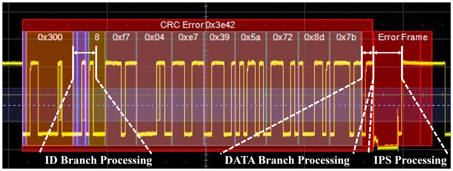
Figure 11 shows actual measured waveforms obtained by verifying the proposed IDS/IPS on the FPGA. The ID branch processing and DATA branch processing regions indicated in the figure correspond to the intervals in which the computations of the two branches are actually performed along the time axis during CAN frame reception. In addition, the IPS processing and error frame regions on the right show the process in which the IPS operates on a frame judged to be an attack and generates an error frame through the CAN controller. That is, the proposed architecture not only detects abnormal CAN traffic but also demonstrates that the IDS decision can trigger the IPS generator at the hardware level. These measured results support that the computation and IDS-triggered IPS operation of the proposed architecture can be performed continuously in the FPGA-based CAN verification setup. Together with the timing margin and detection latency results presented earlier, they also support the feasibility of frame-level detection and hardware-level IPS triggering in resource-constrained ECU-oriented implementations.
Because IPS operation may block a legitimate CAN frame or miss an attack frame depending on the decision threshold, the threshold-dependent false-blocking and missed-attack behavior was evaluated on the validation set. Table 11 summarizes the FP/FN trend for sigmoid decision thresholds from 0.1 to 0.9. As the threshold increased, false positives decreased, whereas false negatives increased. This reflects the expected IPS trade-off: a lower threshold increases attack sensitivity but may increase false blocking, whereas a higher threshold reduces false blocking but may increase missed attacks.
Figure 11. Measured FPGA waveforms showing hardware-level triggering of error-frame generation by the IDS/IPS path in the FPGA-based CAN verification setup. Colored overlays denote decoded CAN fields, and white dashed annotations mark the ID, DATA, and IPS processing intervals.
Electronics 15 02108 g011
Table 11. Threshold-dependent FP/FN behavior for IDS-triggered IPS operation on the validation set.
Sigmoid ThresholdFPFNFalse-Blocking Rate (%)Missed-Attack Rate (%)F1-Score (%)
0.141160.001520.0026299.9953
0.234190.001260.0031199.9957
0.330260.001110.0042699.9954
0.430310.001110.0050899.9950
0.530330.001110.0054199.9948
0.628390.001040.0063999.9945
0.727420.001000.0068899.9943
0.827490.001000.0080399.9938
0.924550.000890.0090199.9935
At the adopted threshold of 0.5, corresponding to a logit threshold of 0, the proposed model produced 30 false positives among 2,703,525 normal frames and 33 false negatives among 610,372 attack frames, corresponding to false-blocking and missed-attack rates of 0.00111% and 0.00541%, respectively. Although the highest F1-score in the validation-set sweep was observed at a threshold of 0.2, the standard threshold of 0.5 was adopted to avoid validation-set-specific threshold tuning and to implement the FPGA decision as a simple sign check without a sigmoid unit or non-zero threshold comparator. This result reports dataset-level IPS-trigger behavior, not a full vehicle-level safety evaluation.

6.6. ASIC Implementation

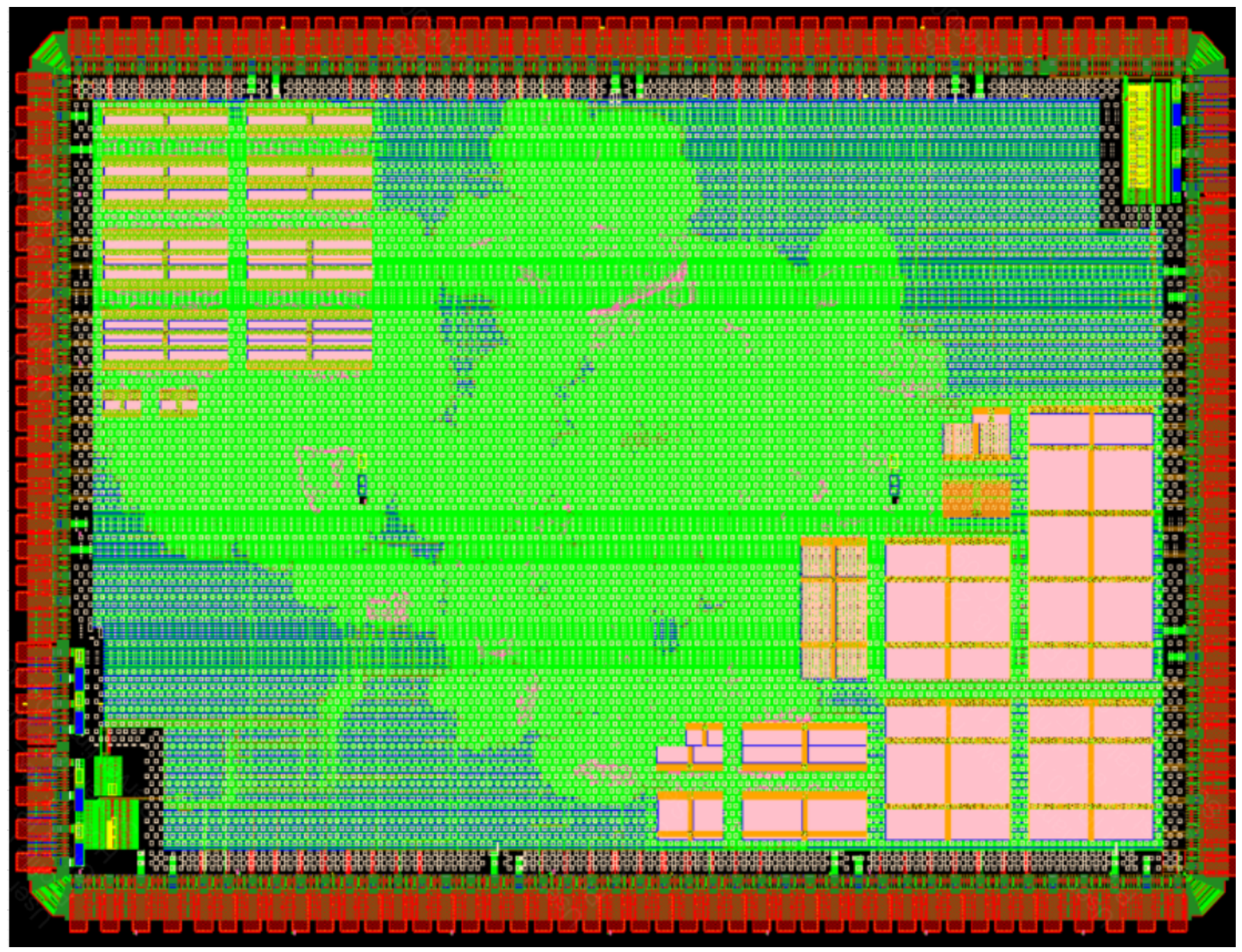
To verify the feasibility of chip-level implementation of the proposed IDS, ASIC synthesis and layout implementation were performed based on the TSMC 28 nm process beyond FPGA-level verification. The system clock was set to 50 MHz in consideration of real-time operation in automotive ECU environments, and the gate count was calculated on the basis of a two-input NAND gate. Figure 12 shows the ASIC layout of the entire Multi-Project Wafer (MPW) integrated system, and Table 12 presents the comparison of ASIC implementation complexity between LC-IDS and the proposed IDS.
Figure 12 shows the ASIC layout of the MPW integrated system implemented based on the TSMC 28 nm process. This layout is not the placement result of a standalone chip containing only the proposed IDS, but rather a system-level implementation result in which multiple modules are included together. Therefore, the total chip area shown in the figure should not be interpreted as the area of the proposed IDS itself. Nevertheless, this layout shows that the proposed IDS can be implemented at the system level even in an actual MPW integrated environment and supports its feasibility for chip-level integration.
Figure 12. ASIC layout of a multi-purpose test chip including the proposed IDS. The colors indicate different physical layout layers in the IC layout view and are used for visual distinction.
Electronics 15 02108 g012
Table 12 presents the system-level ASIC implementation comparison between the LC-IDS baseline and the proposed COL-IDS. Both architectures were synthesized under the same 50 MHz system clock condition and include the same CAN controller. Compared with the LC-IDS baseline, the proposed COL-IDS reduced the IDS logic size from 37,545 gates to 29,318 gates and the SRAM-equivalent area from 62,142 gates to 22,541 gates. As a result, the total chip gate count was reduced from 118,420 gates to 70,592 gates.
This reduction is mainly attributed to the joint software-level and hardware-level lightweighting. At the software level, COL-IDS replaces the seven-frame ID sequence used in LC-IDS with a single-frame ID feature, thereby reducing the number of parameters required for inference and the corresponding SRAM requirement. At the hardware level, the LC-IDS RTL baseline was implemented with five PEs in the Dense1 layer, whereas COL-IDS uses two PEs and temporally distributes the computation through the streaming pipeline. Therefore, COL-IDS reduces both parameter-storage SRAM and computation logic while satisfying the required branch-wise timing constraint.
The power estimates show the same trend. COL-IDS reduces the total estimated ASIC power from 2.9375 mW to 2.0231 mW and the memory-group power from 1.8381 mW to 0.6387 mW, corresponding to reductions of 31.13% and 65.25%, respectively. For energy estimation, the full active inference time was computed as the sum of the ID-branch and DATA-branch active latencies. Although COL-IDS has a slightly longer full active inference time because of the reduced PE parallelism, its lower total estimated power reduces the active inference energy from 47.41 nJ to 34.68 nJ, corresponding to a 26.86% reduction. These values should be interpreted as implementation-level estimates under the stated synthesis condition: absolute power and energy may vary depending on process corner, voltage, temperature, switching activity, and SRAM macro/model assumptions.
Table 12. System-level ASIC gate-count, power, and active-inference-energy comparison between the LC-IDS baseline and the proposed COL-IDS.
MetricLC-IDSProposed IDS
System clock50 MHz50 MHz
CAN Controller18,733 gate18,733 gate
IDS Logic37,545 gate29,318 gate
Total area of SRAM62,142 gate22,541 gate
Total area of Chip118,420 gate70,592 gate
Operating voltage1.62 V1.62 V
Cell leakage power2.0570 mW1.2171 mW
Total dynamic power0.8805 mW0.8061 mW
Total estimated power2.9375 mW2.0231 mW
Memory-group power1.8381 mW0.6387 mW
Full active inference time16.14  μ s17.14  μ s
Full active inference energy47.41 nJ34.68 nJ

7. Discussion and Limitations

7.1. Single-Frame Detection Scope

The proposed COL-IDS uses only the ID and DATA fields of the current CAN frame. This hardware-oriented simplification reduces buffering, parameter storage, and computation cost, but it does not explicitly model temporal order, message frequency, inter-arrival time, or cross-frame context. Therefore, the reported results should be interpreted as supervised frame-level detection performance for known message-injection patterns represented in the training distribution, rather than as evidence of robustness to general temporal or frequency-based CAN anomalies.
The ablation results show that the evaluated HCRL traces contain strong single-frame cues, especially for known injected ID/DATA patterns. Thus, the high performance on DoS, Gear, and RPM scenarios should be interpreted as the detection of known frame-level injection patterns in the evaluated traces, not as proof of robustness to frequency-only DoS attacks or unseen spoofing patterns that preserve legitimate-looking ID/DATA values.

7.2. Replay Attack Limitation

Replay attacks are a representative limitation of the current single-frame ID/DATA-based design. If a previously observed normal frame is retransmitted with the same ID and DATA values, the proposed classifier receives the same input features as the original normal frame. Therefore, without temporal freshness information, sequence-level context, or authentication, exact replayed frames cannot be structurally distinguished from the original normal frames.
To quantify this limitation, an additional software-level replay analysis was performed using replay attack samples from the HCRL In-Vehicle Network Intrusion Detection Challenge Dataset [22]. The proposed COL-IDS achieved 77.89% Precision, 49.98% Recall, and 60.89% F1-score for the replay scenario. The corresponding confusion matrix was TP = 22,761, TN = 124,875, FP = 6461, and FN = 22,776, resulting in an empirical evasion rate of FN/(TP + FN) = 50.02%. This result indicates that robust replay detection requires temporal context, freshness checking, or authentication-based mechanisms beyond the current lightweight frame-level architecture.

7.3. Deployment-Level Validation Scope

The revised non-shuffled temporal-block holdout protocol reduces leakage risk caused by random mixing of temporally adjacent frames, and the HCRL Survival Analysis Dataset provides additional dataset-level validation. However, these experiments do not replace cross-session, strict train-on-one-vehicle/test-on-another-vehicle, real-driving, or unseen-attack evaluation.
In addition, the timing analysis and IPS verification should be interpreted as architectural and hardware-level feasibility results under the evaluated CAN 2.0B conditions, not as complete system-level validation under all bus-load, retransmission, or vehicle safety conditions. Extending the proposed architecture to CAN FD, broader vehicle datasets, temporal features, and system-level IPS safety validation remains future work.

8. Conclusions

In this study, the existing LC-IDS was redesigned from a hardware-oriented perspective to develop a lightweight real-time IDS/IPS architecture for ECU-edge CAN environments. The seven-frame ID sequence input of LC-IDS was simplified into a single CAN ID-based structure, eliminating multi-frame ID buffering. As a result, the FLOPs were reduced from 11,242 to 4522, and the number of parameters was reduced from 4045 to 1789, while maintaining detection performance comparable to that of the existing LC-IDS for known frame-level message-injection scenarios.
The proposed COL-IDS was evaluated on the Car-Hacking Dataset under the revised non-shuffled temporal-block holdout protocol, and additional validation on the HCRL Survival Analysis Dataset showed that the same frame-level ID/DATA architecture can also be applied to another public CAN IDS dataset without structural modification.
For hardware implementation, a streaming pipeline and computation–resource–reuse architecture were applied to reduce hardware cost without excessive parallel expansion. The existing LC-IDS was also implemented as an RTL baseline under the same platform and design constraints for a controlled comparison. On the Nexys A7-100T FPGA platform, the proposed architecture achieved a DATA-complete-to-decision latency of 5.68 μ s after ID-branch precomputation at 50 MHz, while the ID-branch precomputation latency was 11.46 μ s. The branch-wise timing analysis confirmed that both branches satisfy their timing budgets under the CAN 2.0B extended-frame, 1 Mbps, non-empty DATA-frame condition. Compared with the baseline LC-IDS in the same FPGA environment, the proposed architecture reduced LUT, FF, and BRAM usage by 20.16%, 16.63%, and 60.89%, respectively. In addition, ASIC synthesis using the TSMC 28 nm process showed that the proposed architecture can be implemented with a total of 70,592 gates, while reducing the total estimated ASIC power and active inference energy by 31.13% and 26.86%, respectively, compared with the LC-IDS baseline.
The measured FPGA waveforms further verified that the IDS decision can trigger the IPS generator and produce an error frame through the CAN controller in the FPGA-based CAN verification setup, demonstrating the hardware-level feasibility of IDS-triggered IPS operation.
Future work will extend the proposed approach to unseen attacks, replay attacks, cross-session and cross-vehicle distribution shifts, and real-driving conditions. In addition, system-level timing and safety analysis under diverse traffic conditions, including false-blocking effects and safety-critical control traffic, will be conducted to evaluate practical in-vehicle deployment more comprehensively.

Author Contributions

Conceptualization, Y.J. and S.L.; methodology, Y.J., H.I., J.K., S.K. and E.K.; software, Y.J., H.I., J.K. and S.K.; validation, Y.J.; formal analysis, Y.J.; investigation, Y.J., J.K., S.K. and E.K.; resources, S.L.; data curation, Y.J.; writing—original draft preparation, Y.J.; writing—review and editing, H.I. and S.L.; visualization, Y.J.; supervision, S.L.; project administration, S.L.; funding acquisition, S.L. All authors have read and agreed to the published version of the manuscript.

Funding

This work was supported by Korea Evaluation Institute of Industrial Technology (KEIT) grants funded by the Korea Government (MOTIE) (RS-2022-00155731, RS-2023-00232192, RS-2024-00403397, and RS-2024-00433615), and in part by National Research Foundation of Korea (NRF) funded by the Korea Government (MSIT) (2021M3H2A1038042).

Informed Consent Statement

Not applicable.

Data Availability Statement

Acknowledgments

The draft manuscript was translated into English by ChatGPT (GPT-5.5, OpenAI, San Francisco, CA, USA), and then it was carefully reviewed and revised by the authors.

Conflicts of Interest

The authors declare no conflicts of interest.

References

  1. Bosch. CAN Specification Version 2.0; Robert Bosch GmbH: Stuttgart, Germany, 1991. [Google Scholar]
  2. Lokman, S.-F.; Othman, A.T.; Abu-Bakar, M.-H. Intrusion Detection System for Automotive Controller Area Network (CAN) Bus System: A Review. EURASIP J. Wirel. Commun. Netw. 2019, 2019, 184. [Google Scholar] [CrossRef]
  3. Luo, F.; Wang, J.; Zhang, X.; Jiang, Y.; Li, Z.; Luo, C. In-Vehicle Network Intrusion Detection Systems: A Systematic Survey of Deep Learning-Based Approaches. PeerJ Comput. Sci. 2023, 9, e1648. [Google Scholar] [CrossRef] [PubMed]
  4. Lampe, B.; Meng, W. A Survey of Deep Learning-Based Intrusion Detection in Automotive Applications. Expert Syst. Appl. 2023, 221, 119771. [Google Scholar] [CrossRef]
  5. Wang, K.; Zhang, A.; Sun, H.; Wang, B. Analysis of Recent Deep-Learning-Based Intrusion Detection Methods for In-Vehicle Network. IEEE Trans. Intell. Transp. Syst. 2023, 24, 1843–1854. [Google Scholar] [CrossRef]
  6. Gao, S.; Zhang, L.; He, L.; Deng, X.; Yin, H.; Zhang, H. Attack Detection for Intelligent Vehicles via CAN-Bus: A Lightweight Image Network Approach. IEEE Trans. Veh. Technol. 2023, 72, 16624–16636. [Google Scholar] [CrossRef]
  7. Im, H.; Lee, S. TinyML-Based Intrusion Detection System for In-Vehicle Network Using Convolutional Neural Network on Embedded Devices. IEEE Embed. Syst. Lett. 2025, 17, 67–70. [Google Scholar] [CrossRef]
  8. Kang, M.-J.; Kang, J.-W. Intrusion Detection System Using Deep Neural Network for In-Vehicle Network Security. PLoS ONE 2016, 11, e0155781. [Google Scholar] [CrossRef] [PubMed]
  9. Song, H.M.; Woo, J.; Kim, H.K. In-Vehicle Network Intrusion Detection Using Deep Convolutional Neural Network. Veh. Commun. 2020, 21, 100198. [Google Scholar] [CrossRef]
  10. Lo, W.; Alqahtani, H.; Thakur, K.; Almadhor, A.; Chander, S.; Kumar, G. A Hybrid Deep Learning Based Intrusion Detection System Using Spatial–Temporal Representation of In-Vehicle Network Traffic. Veh. Commun. 2022, 35, 100471. [Google Scholar] [CrossRef]
  11. Hanselmann, M.; Strauss, T.; Dormann, K.; Ulmer, H. CANet: An Unsupervised Intrusion Detection System for High Dimensional CAN Bus Data. IEEE Access 2020, 8, 58194–58205. [Google Scholar] [CrossRef]
  12. Agrawal, K.; Alladi, T.; Agrawal, A.; Chamola, V.; Benslimane, A. NovelADS: A Novel Anomaly Detection System for Intra-Vehicular Networks. IEEE Trans. Intell. Transp. Syst. 2022, 23, 22596–22606. [Google Scholar] [CrossRef]
  13. Khandelwal, S.; Shreejith, S. A Lightweight FPGA-Based IDS-ECU Architecture for Automotive CAN. In Proceedings of the 2022 International Conference on Field-Programmable Technology (ICFPT), Hong Kong, China, 5–9 December 2022; IEEE: Piscataway, NJ, USA; pp. 1–9. [CrossRef]
  14. Khandelwal, S.; Shreejith, S. A Lightweight Multi-Attack CAN Intrusion Detection System on Hybrid FPGAs. In Proceedings of the 2022 32nd International Conference on Field-Programmable Logic and Applications (FPL), Belfast, UK, 29 August–2 September 2022; IEEE: Piscataway, NJ, USA; pp. 425–429. [CrossRef]
  15. Rangsikunpum, A.; Amiri, S.; Ost, L. An FPGA-Based Intrusion Detection System Using Binarised Neural Network for CAN Bus Systems. In Proceedings of the 2024 IEEE International Conference on Industrial Technology (ICIT), Bristol, UK, 25–27 March 2024; IEEE: Piscataway, NJ, USA; pp. 1–6. [CrossRef]
  16. Choi, M.; Lee, M.; Im, H.; Lee, J.; Lee, S. Shallow Learning-Based Intrusion Detection System for In-Vehicle Network: ASIC Implementation. Electronics 2025, 14, 683. [Google Scholar] [CrossRef]
  17. HCRL. Car-Hacking Dataset. Available online: https://ocslab.hksecurity.net/Datasets/car-hacking-dataset (accessed on 4 May 2026).
  18. HCRL. Survival Analysis Dataset for Automobile IDS. Available online: https://ocslab.hksecurity.net/Datasets/survival-ids (accessed on 4 May 2026).
  19. Sze, V.; Chen, Y.-H.; Yang, T.-J.; Emer, J.S. Efficient Processing of Deep Neural Networks: A Tutorial and Survey. Proc. IEEE 2017, 105, 2295–2329. [Google Scholar] [CrossRef]
  20. Moolchandani, D.; Kumar, A.; Sarangi, S.R. Accelerating CNN Inference on ASICs: A Survey. J. Syst. Archit. 2021, 113, 101887. [Google Scholar] [CrossRef]
  21. Jacob, B.; Kligys, S.; Chen, B.; Zhu, M.; Tang, M.; Howard, A.; Adam, H.; Kalenichenko, D. Quantization and Training of Neural Networks for Efficient Integer-Arithmetic-Only Inference. In Proceedings of the IEEE/CVF Conference on Computer Vision and Pattern Recognition (CVPR), Salt Lake City, UT, USA, 18–22 June 2018; IEEE: Piscataway, NJ, USA; pp. 2704–2713. [CrossRef]
  22. HCRL. In-Vehicle Network Intrusion Detection Challenge. Available online: https://ocslab.hksecurity.net/Datasets/datachallenge2019/car (accessed on 4 May 2026).
Figure 1. CAN 2.0B Frame.
Electronics 15 02108 g001
Figure 2. Architecture of the proposed CAN IDS.
Electronics 15 02108 g002
Figure 4. Fixed-point format used in this work: integer part (6 bits) and fractional part (9 bits).
Electronics 15 02108 g004
Figure 5. Proposed PE architectures: (a) a dense-layer PE with a 32-bit intermediate MAC datapath and a scaler and (b) a binary convolution PE with mask generation and a bitwise-AND-based accumulation structure.
Electronics 15 02108 g005
Figure 6. Parameter supply architecture with SRAM and on-chip parameter buffer. The red arrow indicates the dedicated Dense1 weight-streaming path.
Electronics 15 02108 g006
Figure 7. Processing flow of a streaming step in the DATA branch. Colored regions indicate the convolution windows used to generate the convolution outputs.
Electronics 15 02108 g007
Figure 8. Operation scheduling.
Electronics 15 02108 g008
Figure 9. FPGA-based verification environment for the proposed COL-IDS. (a) Block diagram of the verification setup. (b) Photograph of the actual hardware verification setup.
Electronics 15 02108 g009
Figure 10. Timing margin of the ID and DATA branches in a classical CAN 2.0B extended frame.
Electronics 15 02108 g010
Table 1. Model complexity and frame-level decision characteristics.
LC-IDSProposed
FLOPs11,2424522
Parameters40451789
Detection granularityper CAN frameper CAN frame
Decision availabilityAfter seven-frame bufferingimmediate *
* No multi-frame buffering is required; frame-level inference is available for each received frame.
Disclaimer/Publisher’s Note: The statements, opinions and data contained in all publications are solely those of the individual author(s) and contributor(s) and not of MDPI and/or the editor(s). MDPI and/or the editor(s) disclaim responsibility for any injury to people or property resulting from any ideas, methods, instructions or products referred to in the content.