Article

The Impact of Self-Heating on Single-Event Transient Effect in Triple-Layer Stacked Nanosheets: A TCAD Simulation

1
School of Integrated Circuits, Guizhou Normal University, Guiyang 550025, China
2
International School, Beijing University of Posts and Telecommunications, Beijing 100876, China
3
Institute of Microelectronics of the Chinese Academy of Sciences, Beijing 100029, China
*
Authors to whom correspondence should be addressed.
Electronics 2026, 15(1), 85; https://doi.org/10.3390/electronics15010085 (registering DOI)
Submission received: 17 November 2025 / Revised: 17 December 2025 / Accepted: 18 December 2025 / Published: 24 December 2025

Abstract

This study investigates the impact of the self-heating effect (SHE) on single-event transient (SET) sensitivity in triple-layer stacked nanosheet transistors, using technology computer-aided design (TCAD) simulations. The results demonstrate that SHE significantly elevates the channel lattice temperature under DC bias, leading to notable degradation in DC performance metrics, including the drive current (ION) and the on/off current ratio. By employing a finer time resolution in the AC simulation, we observed that the device reaches thermal equilibrium on a picosecond timescale. Crucially, SHE is found to exacerbate SET sensitivity markedly. Compared to simulations without SHE, the presence of self-heating increases both the peak transient current and the collected charge at the drain terminal following heavy-ion strikes. Furthermore, the transient response is shown to depend on the thermal history; longer pre-strike heating times amplify the SET peak magnitude, whereas longer cooling times attenuate it. These findings underscore the critical importance of co-optimizing thermal management and radiation hardening in the design of advanced nanosheet technologies.

1. Introduction

The relentless scaling of integrated circuits continues to drive the evolution of semiconductor devices toward three-dimensional (3D) architecture [1]. To overcome short-channel effects, novel structures such as FinFETs and Gate-All-Around (GAA) FETs have emerged. GAA-FETs offer superior gate control and larger effective channel widths compared to FinFETs, positioning them as promising replacements for FinFETs in mainstream nanoscale memory and logic circuits [2,3]. Furthermore, the GAA structure inherently isolates the active channel from the substrate, and exhibits a configuration akin to that of radiation-hardened silicon-on-insulator (SOI) transistors, making it highly promising for space applications [4]. However, this advanced device architecture introduces new challenges, most notably the self-heating effect (SHE) [5]. In GAA-FETs, the channel is fully encapsulated by low-thermal-conductivity gate dielectrics, which severely impede heat dissipation and lead to significant localized temperature increases. This thermal confinement degrades carrier mobility, deteriorates electrical characteristics, increases power consumption, and ultimately accelerates device degradation. Previous studies, employing both experimental techniques [6,7,8] and TCAD simulations [9,10], have extensively characterized SHE, revealing its strong dependence on operating conditions, device geometry, and material properties. It has been established that while experimental measurements are invaluable, they face significant challenges in capturing nanosecond-scale internal temperature dynamics, making TCAD simulations an indispensable tool for such investigations.
Beyond terrestrial applications, the inherent radiation tolerance of GAA-FETs makes them highly attractive for space electronics. Their structure provides excellent resilience against total ionizing dose (TID) effects [11]. Consequently, research has intensified on their susceptibility to single-event effects (SEE), induced by high-energy particle strikes. These heavy ions can generate transient currents, leading to operational upsets or even catastrophic failures. TCAD simulations have been instrumental in revealing that radiation sensitivity is linked to the incident location and angle of ions [12], and that geometric scaling, such as narrowing the nanowire width, can effectively mitigate single-event transients (SETs) by reducing charge collection efficiency [13].
Although self-heating effects (SHE) and single-event effects (SEE) have been extensively studied in isolation, their synergistic interplay—particularly under practical operating conditions—remains poorly understood. Existing research on temperature-dependent SEE has largely assumed uniform ambient temperature distributions [14,15], which does not reflect the localized thermal gradients induced by SHE in modern nanoscale devices. While such coupled effects have been examined in LDMOS power devices [16], the influence of SHE on SET GAA-FETs represents a significant and unaddressed gap. This is critical because, in real space environments, devices experience continuous thermal stress from self-heating alongside radiation exposure. The resulting elevated lattice temperature can fundamentally alter SET mechanisms, yet this coupled thermal–radiation interaction remains largely unexplored, limiting accurate reliability prediction and the design of GAA-FETs for extreme environments.
To address this, the authors systematically investigate the coupled self-heating and single-event transient effects in triple-layer stacked nanosheet GAA-FETs, and employ a finer temporal resolution to characterize the internal transient thermal evolution of the device. This work aims to provide theoretical insights that can enhance the reliability assessment of GAA-FETs under realistic space operating conditions.
This paper is organized as follows. Section 2 describes the simulated device structure, calibration methodology, and simulation details. Section 3 presents a detailed analysis and discussion of the simulation results, focusing on the mechanisms of interaction between SHE and SET. Finally, Section 4 provides the conclusions of this work.

2. Device Structure and Simulation Setup

Figure 1a depicts a three-dimensional schematic of the triple-layer stacked nanosheets device constructed in this work using Sentaurus TCAD P_2019.03. Figure 1b shows the cross-sectional view along the designated cut plane. The nanosheet channels have a thickness of 5 nm, a width of 15 nm, and a gate length of 12 nm. The geometric parameters are calibrated according to the IRDS roadmap, ensuring the simulation reflects realistic, aggressively scaled devices. The gate dielectric stack consists of a 0.6 nm thick SiO2 layer and a 1.5 nm thick HfO2 layer. The source/drain regions employ gaussian doping with a concentration of 1.0 × 1021 cm−3, while the channel region has a constant doping concentration of 1.0 × 1015 cm−3, and the bulk doping concentration is 1.0 × 1018 cm−3 [17]. Channel doping is kept low to minimize impurity scattering and enhance carrier mobility, while the source/drain regions are heavily doped to reduce parasitic contact resistance. More detailed parameters are provided in Table 1.
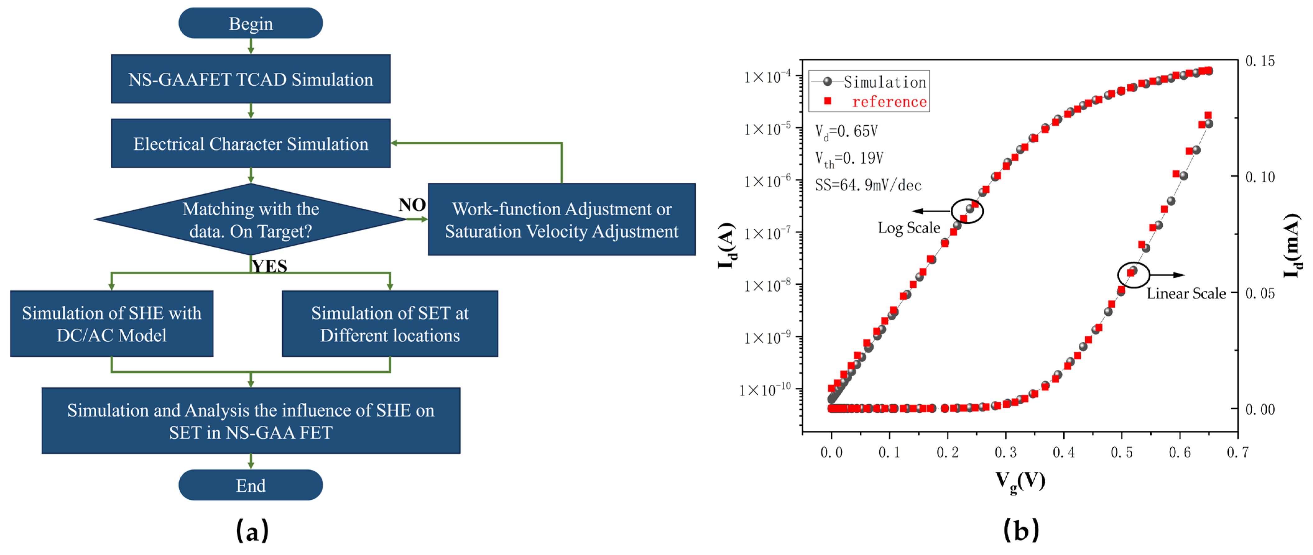
Figure 2a illustrates the workflow of this study, which has been conducted using Sentaurus TCAD software [18]. First, the device structure is created in the Sentaurus Structure Editor. Then, its electrical characteristics are simulated using Sentaurus Device. The simulation incorporated major physical models, including the Fermi-Dirac distribution model, and the bandgap-narrowing models. Carrier generation-recombination processes were accounted for by including the Shockley-Read-Hall (SRH) and Auger recombination models. Carrier mobility was described by the Philips unified mobility model, augmented with the Enormal and thin layer models to incorporate the effects of Coulomb scattering and surface roughness scattering, respectively. The density gradient quantum model (eQuantumPotential) was used for quantum corrections; additionally, the high-field saturation model and a hydrodynamic model were activated. To ensure the accuracy of the simulation results, the gate work function and saturation velocity were calibrated by comparing them with the experimental data from the reported references [17,19], with a drain supply voltage of 0.65 V and the gate voltage swept from 0 to 0.65 V, the Id-Vg characteristic curve was obtained, as shown in Figure 2b. The results demonstrate that the TCAD simulation fits the experimental data well, confirming the validity of the models. The threshold voltage is extracted to be 0.19 V, and the subthreshold swing is 64.9 mV/dec.
Next, the device’s DC/AC thermal characteristics were simulated. To better observe lattice temperature variations and analyze self-heating effects, the thermodynamic model was employed in the TCAD simulations. The thermal conductivities of source/drain, channel, and bulk are 0.1661 W/(cm·K), 0.0807 W/(cm·K), and 1.48 W/(cm·K), respectively [17]. This model effectively describes the device’s thermal characteristics using the current Equation (1). The lattice temperature was calculated as follows [20]:
t c L T κ T = P n T + Φ n J n + P p T + Φ p J p 1 q E C + 3 2 k T J n q R n e t , n 1 q E V + 3 2 k T J p q R n e t , p + ω G o p t J n = n q u n ϕ + P n T J p = p q u p ϕ P p T
where CL is the lattice heat capacity, T is the lattice temperature, and κ is the thermal conductivity. Pn and Pp are the absolute thermoelectric powers for electrons and holes, respectively, while Φn and Φp are the electron and hole quasi-Fermi potentials. The current densities for electrons and holes are Jn and Jp, respectively. EC and EV are the conduction and valence band energies, respectively. Gopt is the optical generation rate from photons with frequency ω. Finally, Rnet,n and Rnet,p are the electron and hole net recombination rates, respectively. Additionally, defining appropriate boundary conditions is essential for calculating the device temperature. A fixed temperature of 300 K was set at the thermal contacts. A thermal boundary resistance of 2 × 10⁻⁶ cm2 K/W was applied to the contact electrodes, and a value of 2 × 10⁻⁴ cm2 K/W was specified for the interface between the silicon and SiO2 layers [17]. The high resistance at the oxide/semiconductor interface represents the critical bottleneck for heat dissipation. More detailed parameters are provided in Table 1. Crucially, to calculate the lattice temperature (as in Equation (1)), the keyword “Temperature” must be integrated into the current equation. If this keyword is omitted, the temperature calculation is skipped, and the software defaults to Equation (2), which does not account for temperature:
J n = n q u n ϕ J p = p q u p ϕ
Thirdly, the simulation methodology for the single-event transients (SETs) is presented in Section 3.2. Lastly, the impact of SHE on SET is investigated.
Table 1. Device parameters and thermal conductivity.
SymbolDescriptionValueSymbolDescriptionValue
LG (nm)Gate Length [19]12WK (eV)Gate Work Function4.48
LSP (nm)Spacer Length [19]5NSD (cm−3)Source/Drain Doping Concentration [17]1 × 10²¹
LSD (nm)Source/Drain Length5.5NChannel (cm−3)Channel Doping Concentration [17]1× 10¹⁵
WNS (nm)Nanosheet Width15Nbulk (cm−3)Bulk Doping Concentration [17]1× 10¹⁸
TNS (nm)Nanosheet Thickness [19]5VDD(V)Supply Voltage0.65
EOT (nm)Effect Oxide Thickness2.1NSS (nm)Nanosheet Spacer7.7
CGP (nm)Contact Gate Pitch34KCh (W/cm·K)Channel Thermal Conductivity [17]0.0807
FP (nm)Fin Pitch24KSD (W/cm·K)Source/Drain Thermal Conductivity [17]0.1661
Tstack (nm)Stack Thickness10Kbulk (W/cm·K)Bulk Thermal Conductivity [17]1.48
Tbulk (nm)Bulk Thickness55Koxide (W/cm·K)Oxide Conductivity0.14
TFin (nm)Fin Thickness50Roxide/si (W/cm−2·K)Distributed Interface Thermal Resistance2 × 10−4

3. Results and Discussion

3.1. DC/AC Characteristic of SHE in Triple-Layer Stacked Nanosheets

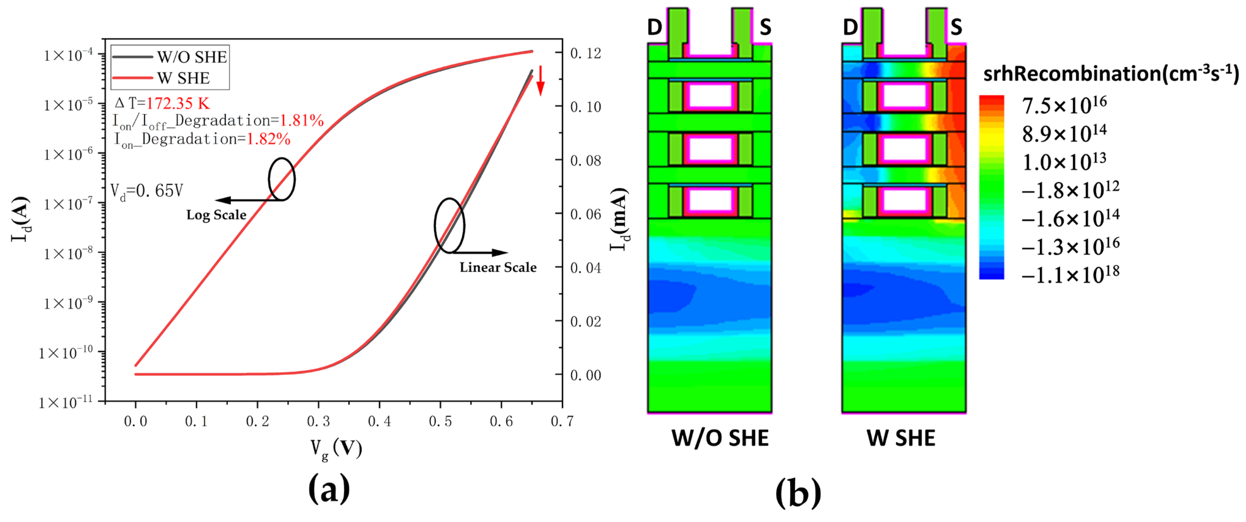
The impact of the self-heating effect (SHE) on device performance was initially evaluated by simulating the device under DC conditions. The transfer characteristics presented in Figure 3a provide quantitative evidence that the SHE suppresses the on-state current (Ion) by approximately 1.81%, resulting in a 1.82% reduction in the on/off current ratio. This degradation in Ion is attributed to elevated lattice temperatures, which intensify carrier scattering and reduce mobility, thereby limiting the device’s electrical performance [21]. Furthermore, the slightly larger degradation in the on/off current ratio implies a concurrent increase in off-state leakage. As shown in Figure 3b, which compares SRH recombination profiles with and without SHE, the inclusion of SHE results in enhanced carrier generation rates [22], evidenced by more negative values in the drain region. This thermally induced generation provides an additional leakage path, confirming that the degradation in the on/off ratio is driven by both the mobility-limited on-current reduction and the thermally activated off-current increase.
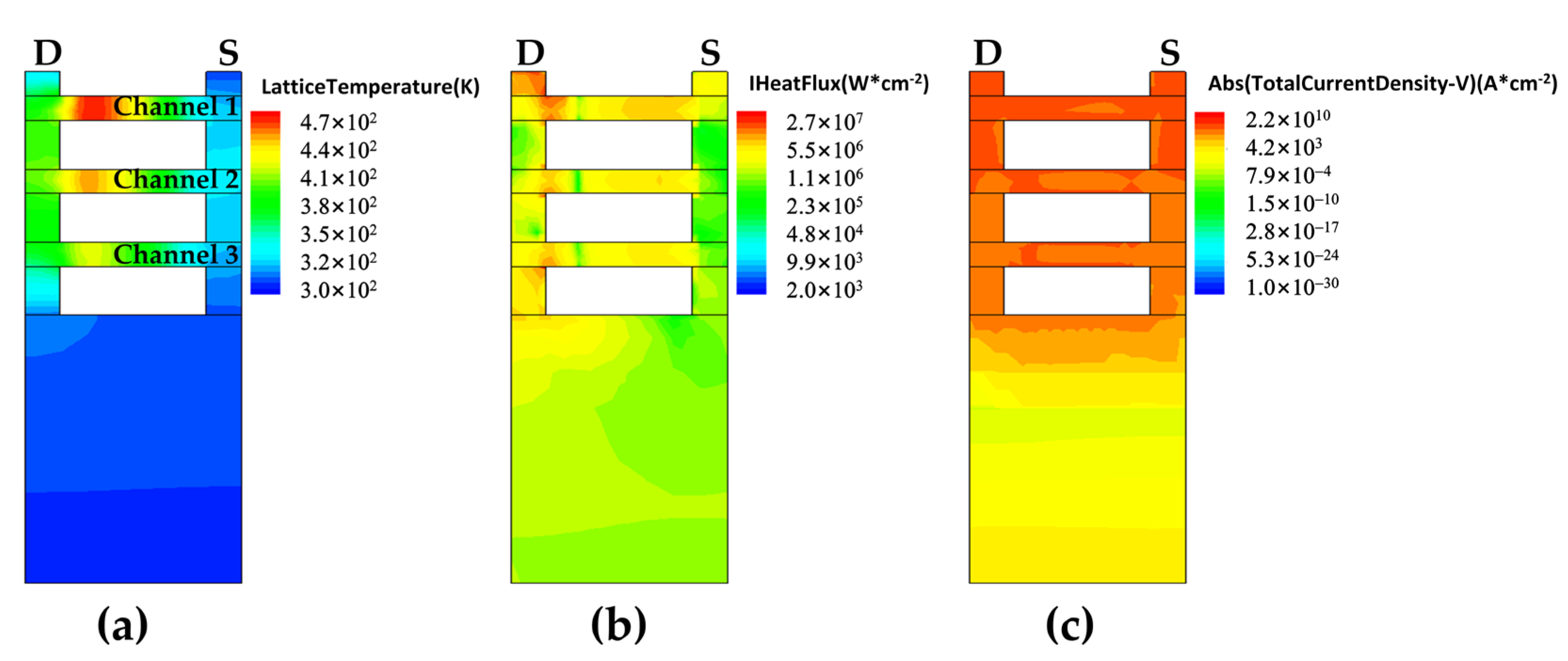
Figure 4a presents the lattice temperature distribution across the cross-section, with a maximum of 472.35 K. It reveals that temperature hotspots primarily occur near the drain side of the channel, with Channel 1 exhibiting the highest temperature compared to Channels 2 and 3. Two main factors can explain this phenomenon. As shown in the heat flux map (Figure 4b), the maximum heat flux occurs near the drain and drain extension regions, indicating the highest heat generation in these areas. Moreover, Channel 1 exhibits greater heat flux than Channels 2 and 3. Additionally, while Channels 2 and 3 can dissipate heat into the substrate, Channel 1’s thermal contact resistance hinders effective heat dissipation, resulting in the highest channel temperature. Compared to Channels 2 and 3, Channel 1 also has the highest current density (Figure 4c). The significant temperature rise in Channel 1 is primarily due to Joule heating, as quantified by Equation (3).
H = J × E
where J is the current density, and E is the electric field [23]. Consequently, the higher current density in Channel 1 results in a corresponding increase in temperature.
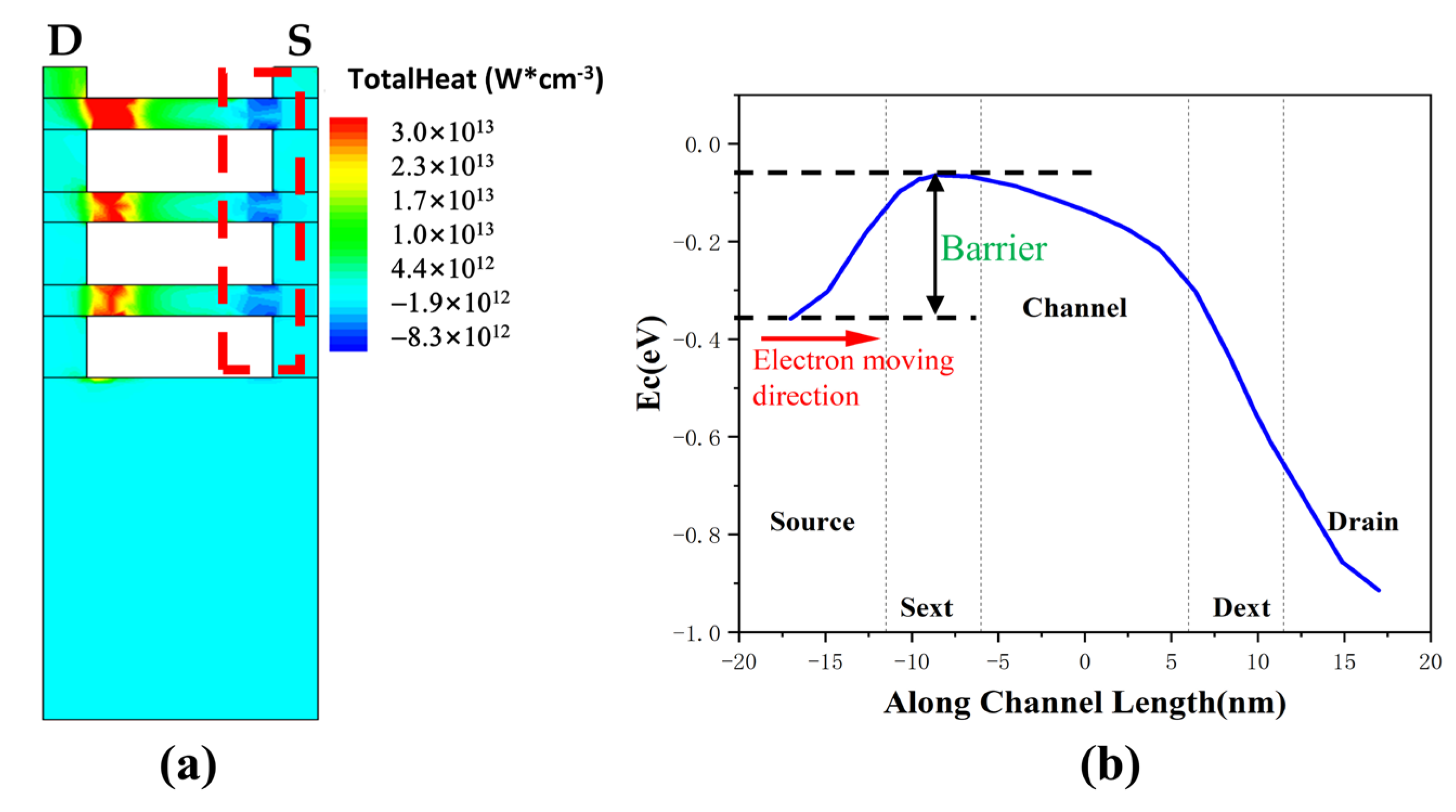
Figure 5a presents the thermal generation rate distribution along the cross-section, revealing a distinct peak on the drain side and a negative thermal generation rate on the source side. This negative thermal generation rate can be attributed to energy absorption processes within the device [24]. Specifically, as shown in Figure 5b, the energy band diagram along the length of Channel 1 indicates that electrons in the source region must absorb energy from the crystal to overcome the potential barrier between the source and the channel. This results in a net phonon absorption process in this region, giving rise to the observed negative thermal generation rate.
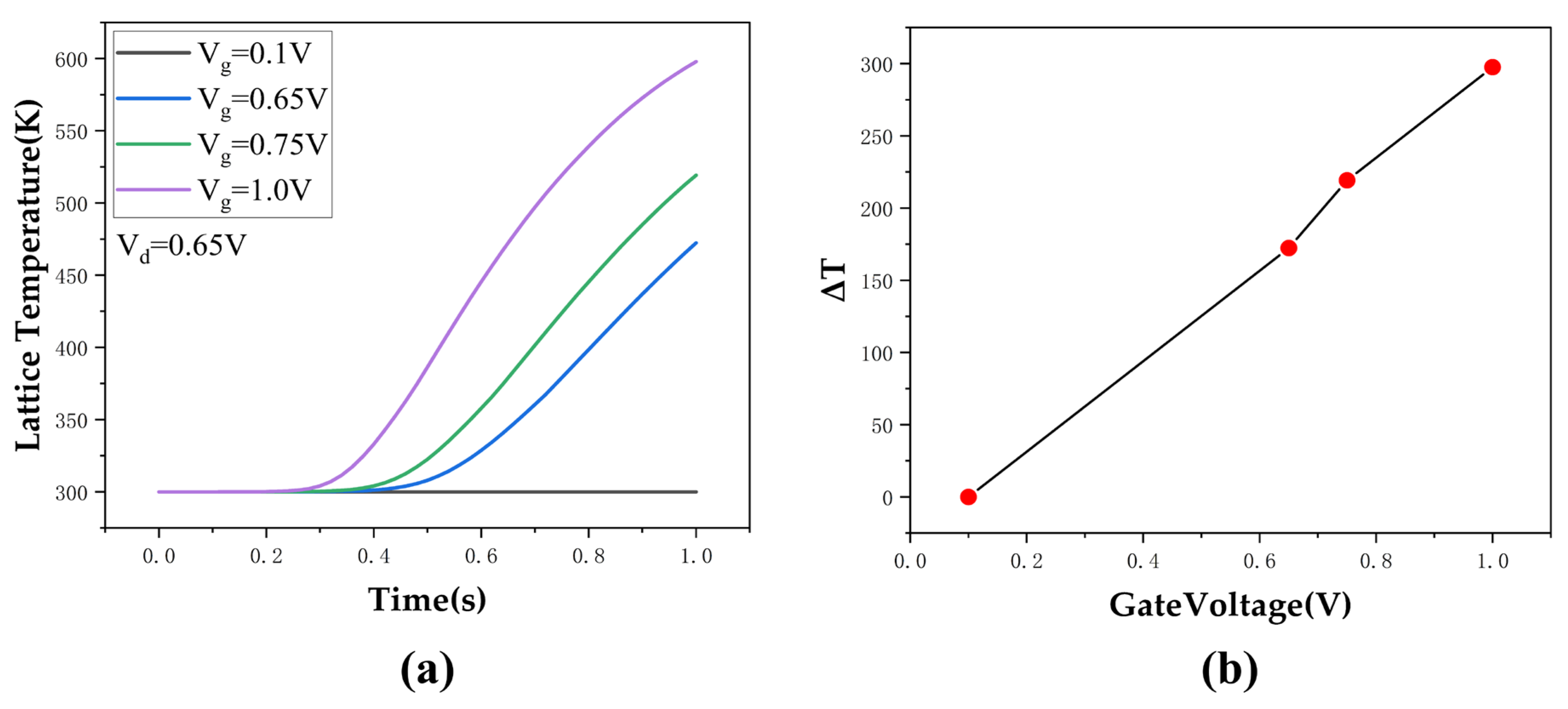
The device’s internal temperature depends on the gate voltage, which is strongly related to the drive current. Figure 6a illustrates the influence of different gate voltages on lattice temperature. When the gate voltage is below the threshold voltage, the carrier concentration remains low, leading to weak self-heating effects and minimal changes in lattice temperature. However, as the gate voltage increases, the carrier concentration within the channel rises significantly. These carriers not only enhance conduction but also intensify thermal-scattering interactions with the crystal medium, leading to substantial increases in temperature variation. Figure 6b clearly demonstrates the trend of this effect as the gate voltage varies.
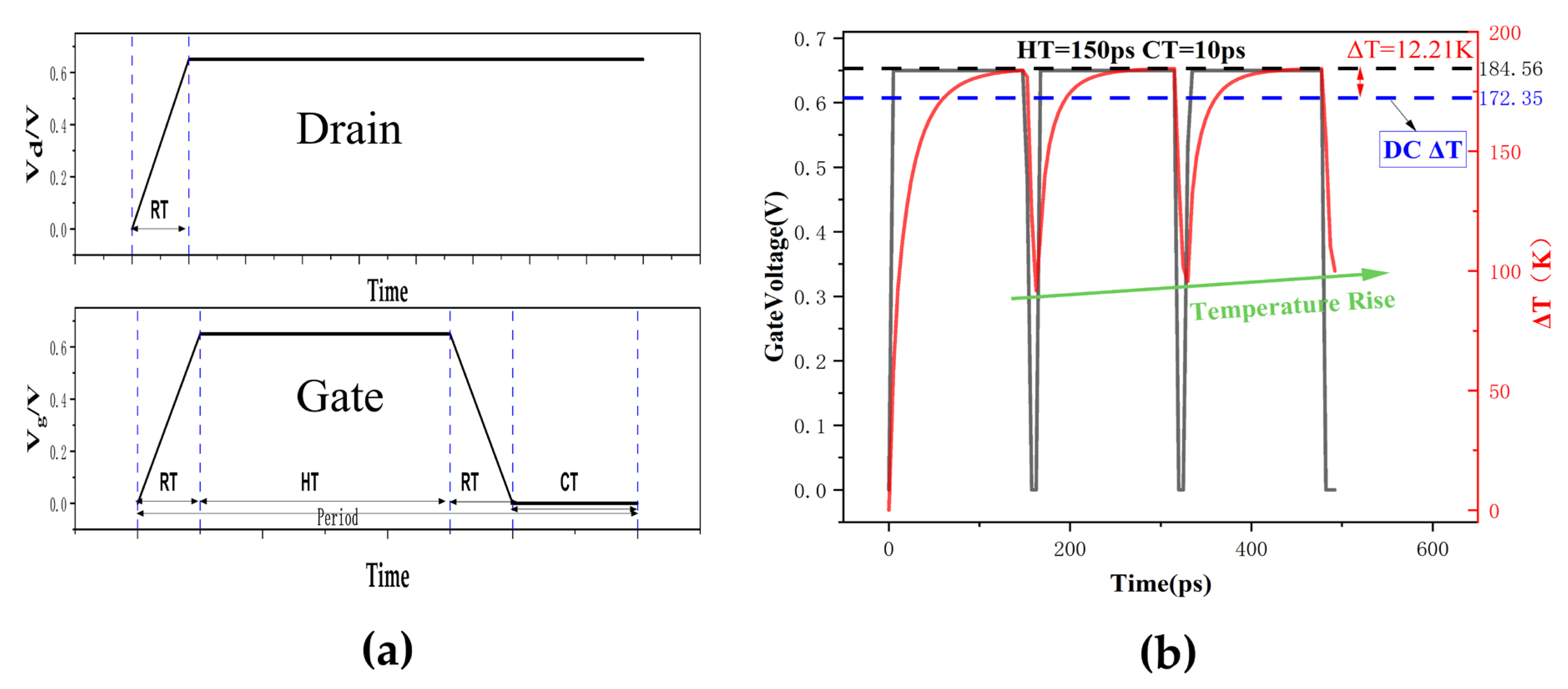
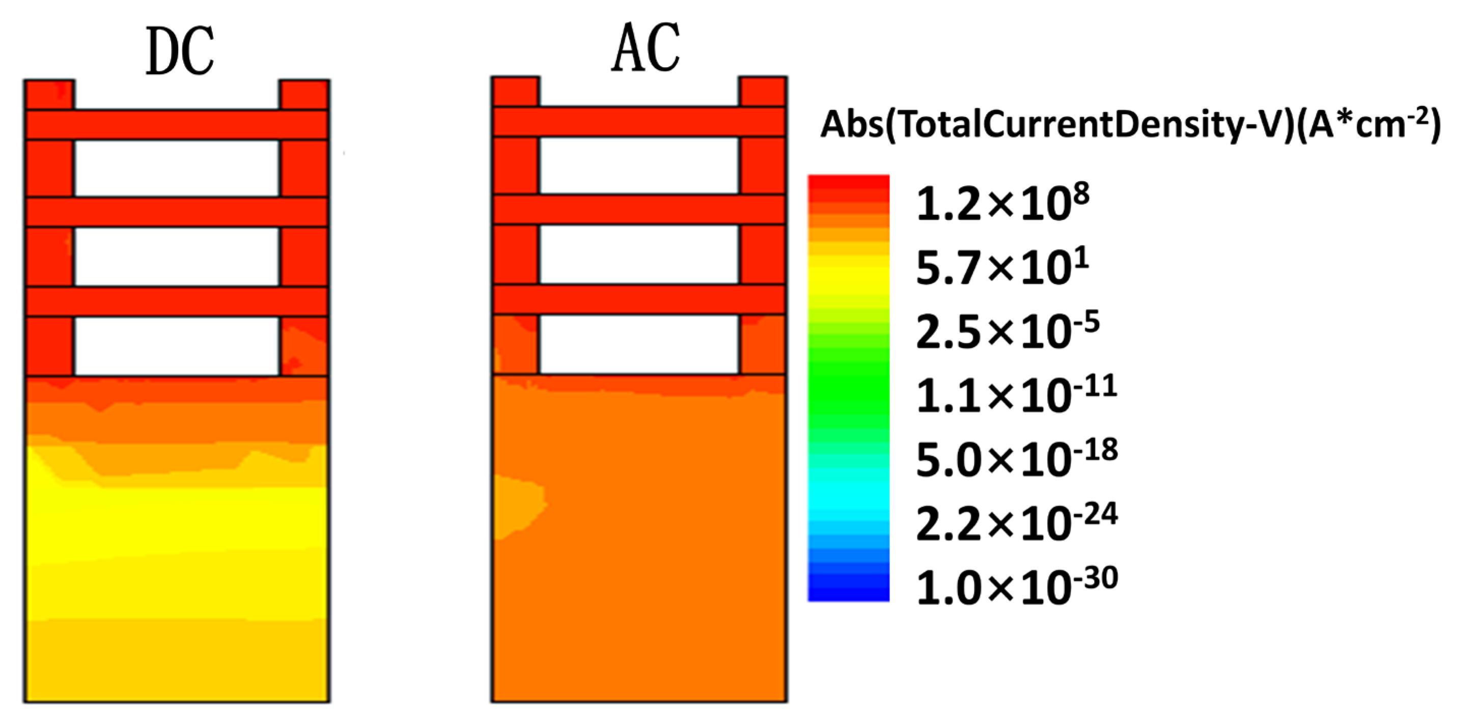
Based on the DC characteristics study, we further investigated the AC characteristics of self-heating effects. Figure 7a illustrates the voltage pulse scheme for the gate and drain terminals. Since the device’s switching behavior is entirely dependent on gate-voltage changes, precise control of self-heating effects can be achieved by modulating the gate-voltage time sequence. Specifically, a complete gate voltage cycle consists of two fast rise times (RT), one adjustable heating time (HT), and one cooling time (CT). The RT is set to 2 ps, to minimize heat dissipation during conduction and ensure measurement accuracy [25,26]. For the drain voltage, a short rise time is applied to reach the target voltage, after which it remains constant to maintain stable measurement conditions. Figure 7b illustrates the applied gate voltage and the corresponding lattice temperature rise as a function of time. The results reveal a rapid increase in lattice temperature upon application of the gate voltage followed by a sharp decrease as the gate voltage is reduced. However, the 10 ps CT is inadequate for complete thermal recovery to the initial state (300 K). Consequently, the device experiences a progressive heat accumulation, resulting in a stepwise increase in the lattice temperature after each pulse, as indicated by the green line. The diagram also shows that the peak temperature rise reaches 184.56 K in AC mode. This value is consistent with the findings in references [27,28]. It exceeds the peak temperature rise in DC mode by 12.21 K. This phenomenon is attributed to a higher instantaneous current density in the AC mode relative to the DC mode. According to Equation (3), this elevated current density results in greater Joule heating, as corroborated by Figure 8.
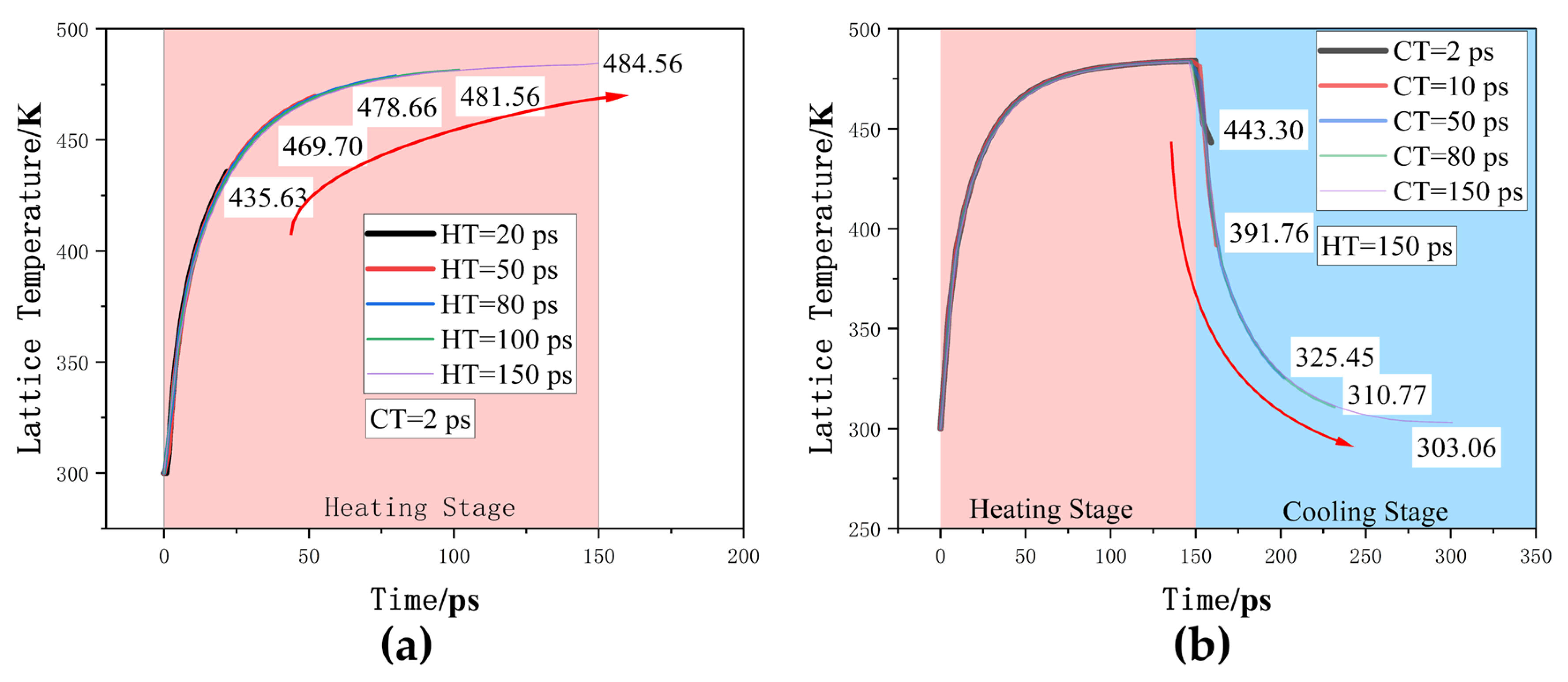
To elucidate the impact of pulse frequency on thermal performance, the lattice temperature dynamics were simulated by systematically varying the HT and CT of the pulse cycle. Figure 9a illustrates the effect of different HT on the lattice temperature under a fixed CT. The lattice temperature shows a clear positive correlation with HT, rising from 435.63 K at HT = 20 ps to an equilibrium temperature of 484.56 K for HT ≥ 150 ps.
Figure 9b presents the influence of different cooling times (CT) on the lattice temperature of the transistor under a fixed heating time (HT = 150 ps). The results show that the lattice temperature exhibits a distinct exponential decay with increasing CT, dropping from 443.30 K at CT = 2 ps to 303.06 K at CT = 150 ps. For CT values of 150 ps or greater, the device effectively returns to its initial ambient temperature (300 K), indicating that complete thermal relaxation is achievable with a sufficient cooling duration. This analysis demonstrates that while prolonged heating time leads to a thermal steady state with diminishing temperature increments, adequate CT is crucial to prevent cumulative heating and ensure the device’s thermal stability.

3.2. The Single-Event Transient Effect in Triple-Layer Stacked Nanosheets

A heavy-ion irradiation model was introduced for SET numerical simulation [29], which is used to calculate and statistically analyze the electron–hole pairs generated and transported in both spatial and temporal dimensions during heavy-ion incidence. In the simulation, the strike radius of 10 nm was adopted, with the LET value fixed at 10 MeV·cm2/mg (1 pC/µm ≈ 100 MeV·cm2/mg [30]). The incident direction was set vertically downward, and the incident length was sufficient to penetrate the entire device. Additionally, the device was biased in the off state [31], meaning the gate, source, and substrate voltages were grounded, and the drain voltage was maintained at 0.65 V.
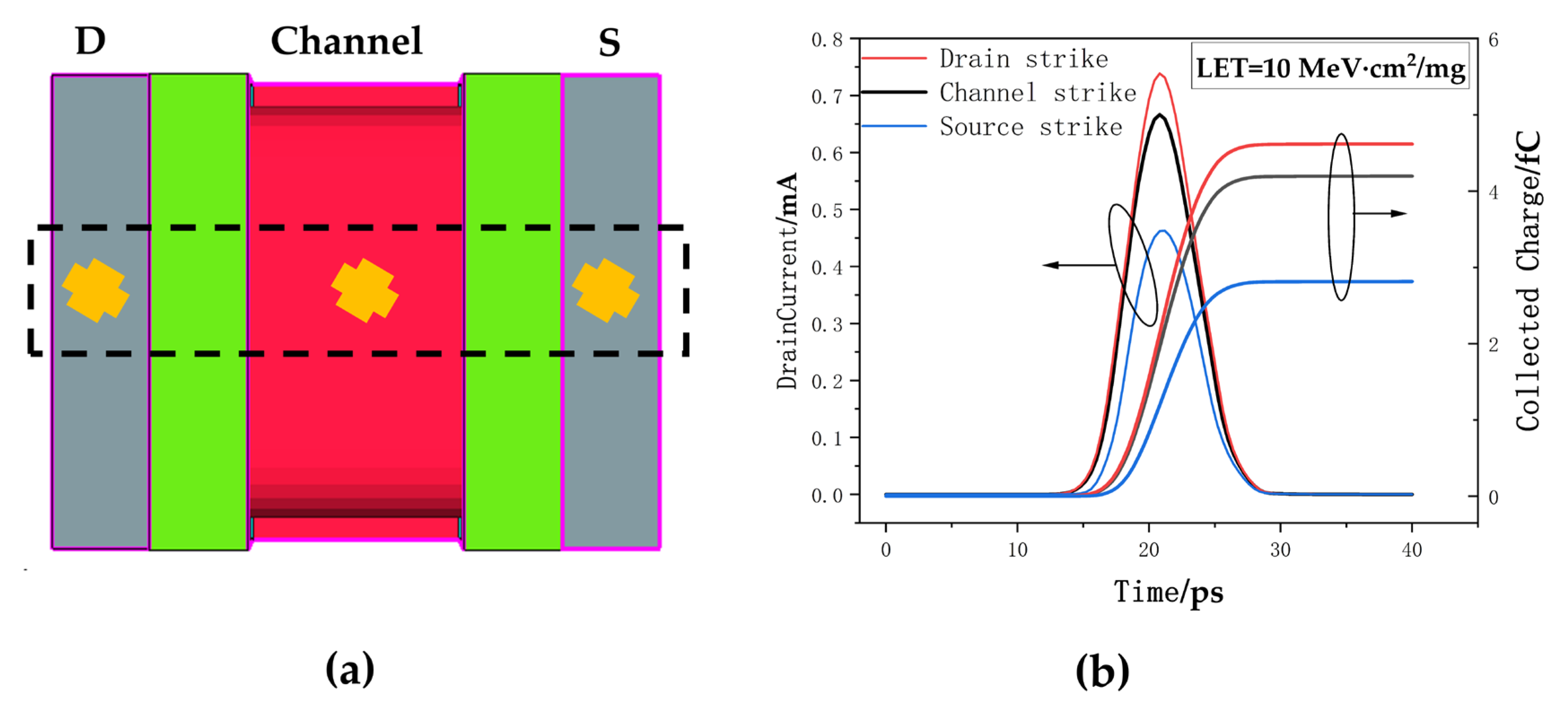
To investigate the sensitivity of the device to heavy ions at different incident positions, we performed heavy-ion irradiation at three distinct locations: the channel center, source terminal, and drain terminal, as illustrated in Figure 10a.
The transient current variations over time under different incident positions are shown in Figure 10b. The results show that the transient current peak reaches a maximum of 738.49 µA when the heavy-ion incidence occurs at the drain terminal. The peak currents decrease to 666.49 µA and 462.79 µA for strikes at the channel center and source terminal, respectively. By calculating the time-integrated transient current at the terminals, the corresponding collected charge values were obtained: 4.62 fC, 4.19 fC, and 2.81 fC for the drain, channel center, and source terminals, respectively. This phenomenon occurs because when heavy ions irradiate the device, they lose energy and generate numerous electron–hole pairs [32]. The high-mobility electrons, under the influence of the built-in electric field between the drain and channel regions and the applied electric field, move in the direction opposite to the electric field lines and are collected by the drain, ultimately forming the transient current. Since the drain has a stronger applied electric field than the channel and source regions, it generates the most significant transient current.
These results demonstrate that the drain terminal exhibits the highest sensitivity to heavy ions, whereas the source terminal shows the lowest.

3.3. The Influence of SHE on SET in Triple-Layer Stacked Nanosheets

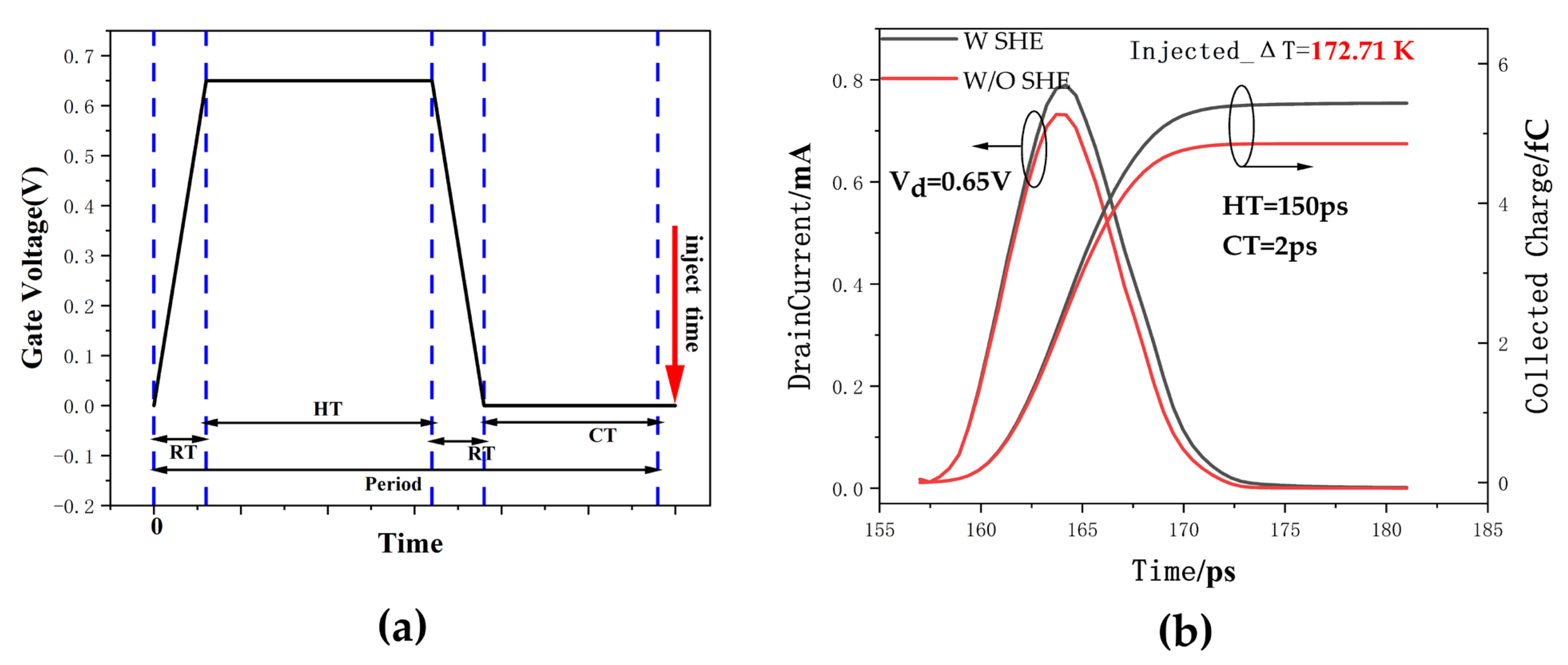
Based on the above work, we investigated the influence of self-heating effects on single-event transient effects in a nanosheet device. As shown in Figure 11a, the gate voltage is applied, and the heavy-ion injection occurs after a complete cycle of the gate voltage waveform. The drain voltage remains constant at 0.65 V throughout the process. Due to the rapid temperature changes within the device, the CT was set to 2 ps (corresponding to the cutoff state, Vg = 0 V) to ensure a fast response to temperature variations. Figure 11b presents the transient current and collected charge versus time curves for this device with and without self-heating effects during heavy-ion transient processes. The lattice temperature during heavy-ion incidence under self-heating effects is 472.71 K. The results demonstrate that the transient response characteristics of the device under self-heating conditions exhibit significant changes compared to the case without self-heating, specifically a noticeable increase in the transient current (from 0.73 mA to 0.79 mA, an increase of approximately 7.9%) and a corresponding rise in collected charge (from 4.85 fC to 5.43 fC, an increase of about 11.9%). These findings further validate the significant impact of self-heating effects on the single-event transient effect of nanosheets.
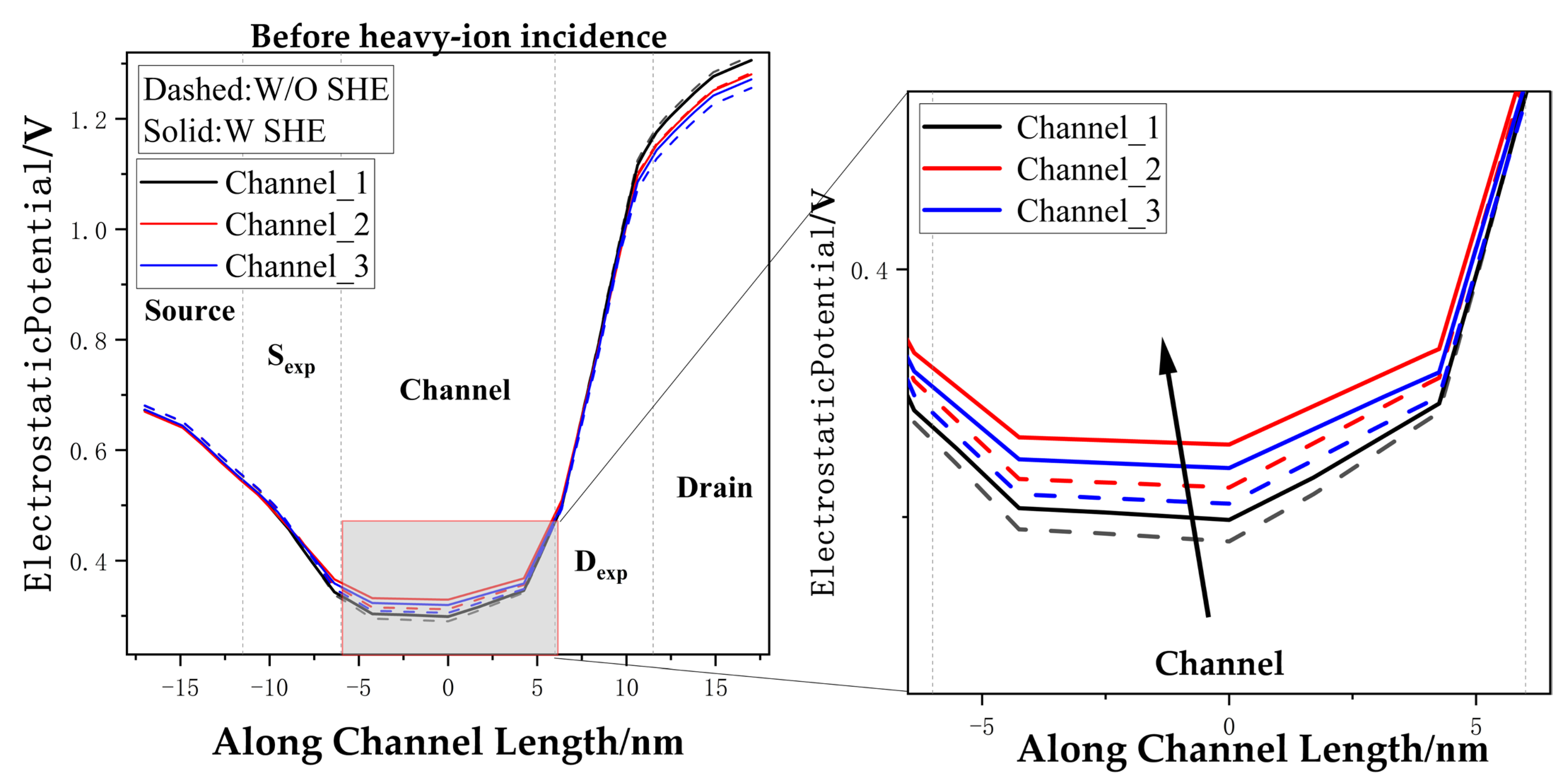
Figure 12 shows the electrostatic potential distribution along the channel length before the heavy-ion strike. As illustrated in the figure, the self-heating effect (SHE) elevates the electric potential across all channels (Channels 1, 2, and 3). This potential elevation subsequently lowers the source-to-channel potential barrier, thereby enhancing the injection of electrons from the source into the channel. These injected electrons then drift towards the drain under the influence of the built-in electric field [33]. Upon the incidence of a heavy ion, the generated electron–hole pairs (EHPs) are separated by this field. The high-mobility electrons are rapidly swept to and collected by the drain. At the same time, the lower-mobility holes tend to accumulate in the channel region, further increasing the channel potential. Once this potential rises sufficiently to forward-bias the source-channel junction, the parasitic bipolar junction transistor (PBJT) is triggered. The activation of this parasitic BJT results in a massive injection of electrons from the source into the channel, which are then collected by the drain, culminating in a significantly amplified transient current response [34].
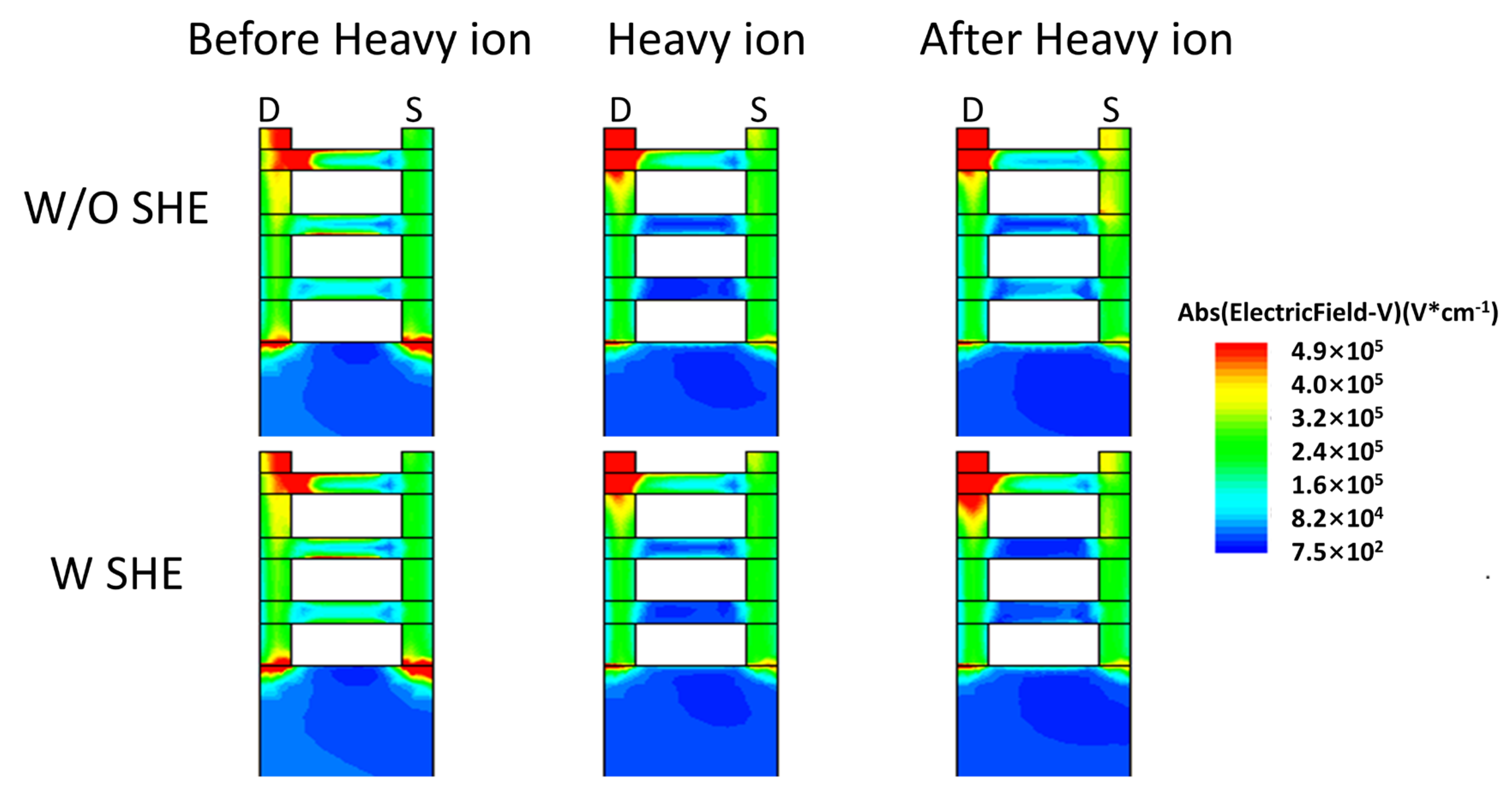
Furthermore, the internal electric field distributions of the device before and after heavy-ion incidence are compared in Figure 13. Following the heavy-ion strike, the internal electric field undergoes a gradual recovery. Compared to the case without SHE, the elevated lattice temperature induced by SHE reduces carrier mobility. This reduced mobility retards the drift and diffusion velocities of the carriers, prolonging the residence time of excess carriers within the device and thereby delaying the recovery of the electric field. Ultimately, this extends the charge collection time window, consequently increasing the total collected charge.
Consequently, the self-heating effect, by pre-elevating the channel potential, effectively reduces the triggering threshold for this parasitic bipolar amplification. This mechanism exacerbates the transient current response induced by heavy-ion incidence, making the device more susceptible to single-event effects. The increase in collected charge under self-heating conditions is attributed to mobility degradation. The lower carrier mobility hinders the evacuation of radiation-induced carriers, extending their residence time in the sensitive volume and leading to a more severe single-event transient response.
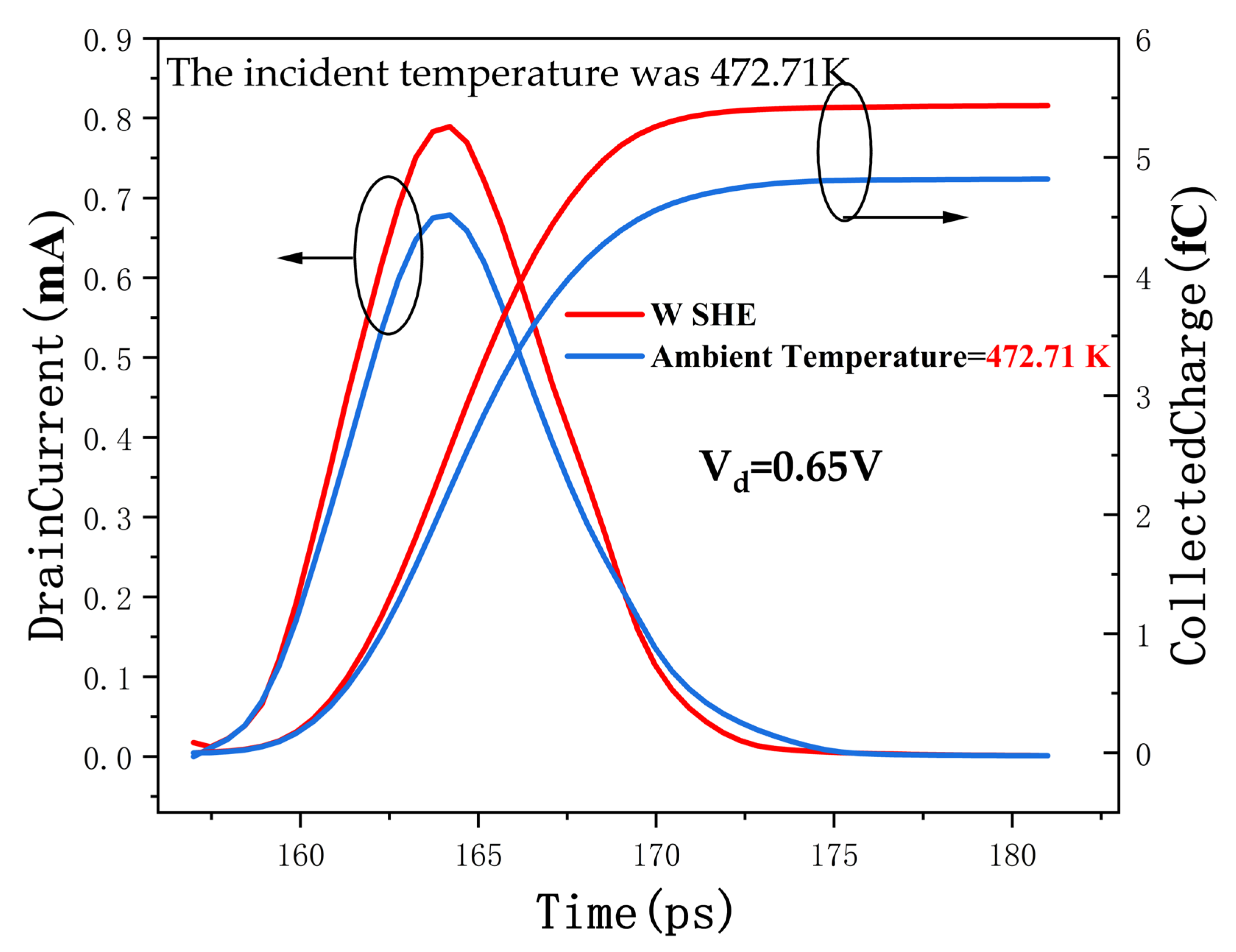
The device temperature under heavy-ion incidence reached 472.71 K due to self-heating. A subsequent SET characterization was therefore conducted at an equivalent ambient temperature. Figure 14 depicts the corresponding variations in transient current and collected charge. The results reveal that, compared to the case influenced solely by ambient temperature (without the self-heating effect), self-heating significantly increases both the peak transient current and the collected charge. Specifically, the peak current rises from 0.68 mA to 0.79 mA (a 16.1% increase), while the collected charge increases from 4.81 fC to 5.43 fC (a 12.9% increase).
These findings confirm that self-heating substantially enhances the sensitivity of nanosheet devices to heavy ions.
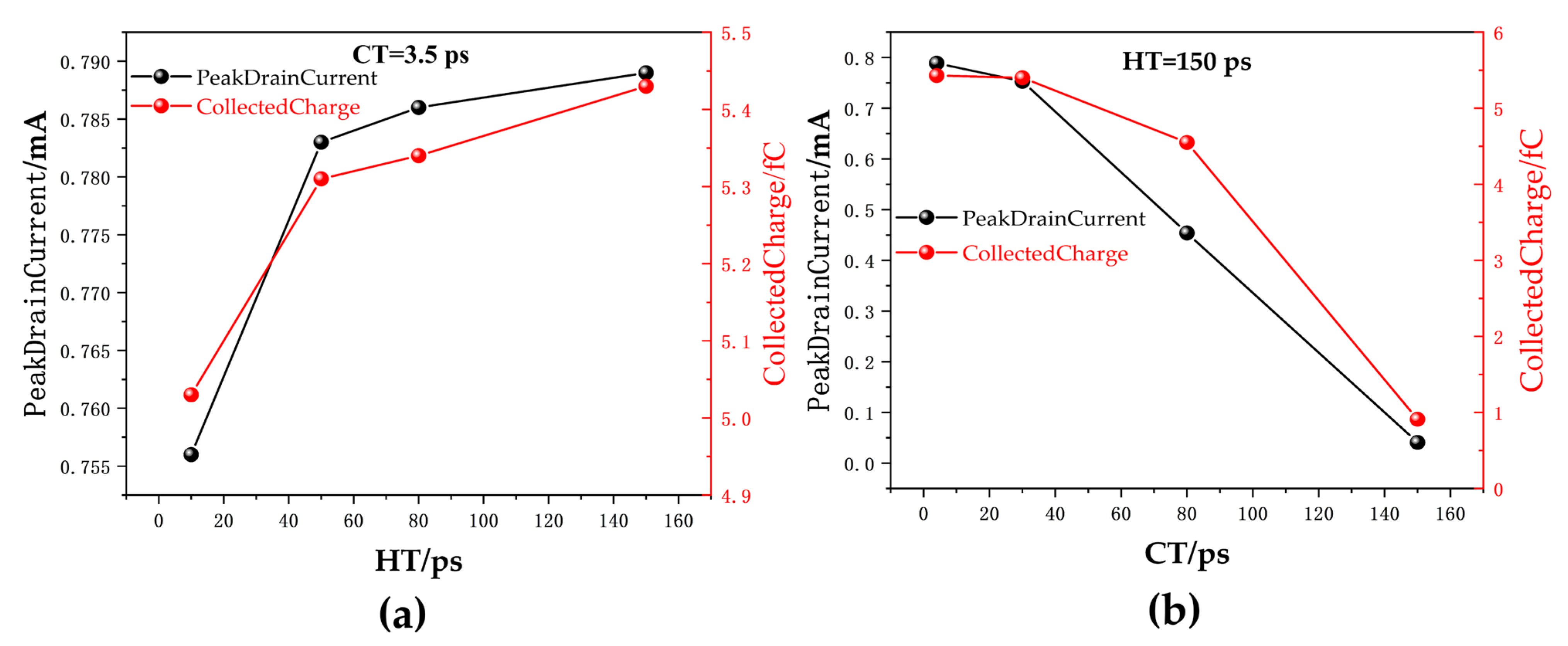
In the AC operating mode, the HT and CT can be flexibly adjusted to investigate their effects on the single-event transients. Simulation results reveal that the peak transient current increases with longer HT, as shown in Figure 15a. The peak transient current increases from 0.76 mA to 0.79 mA, and the collected charge increases from 5.03 fC to 5.43 fC. Conversely, as shown in Figure 15b, under constant HT, the peak transient current decreases with increasing CT, from 0.79 mA to 0.04 mA, accompanied by a reduction in collected charge from 5.43 fC to 0.91 fC. These observations suggest that for HT less than or equal to the thermal equilibrium time, the device’s sensitivity to heavy ions increases with HT but decreases with CT.
Consequently, mitigating NS-FET sensitivity to heavy ions can be achieved by reducing the HT or increasing the CT.

4. Conclusions

This work investigates the self-heating effects, single-event transient effects, and their interplay in triple-layer stacked nanosheets using TCAD simulations. The simulation results reveal that the lattice temperature in the GAA device evolves on a picosecond timescale, reaching thermal equilibrium at approximately 150 ps. In DC operation, the maximum lattice temperature reaches 472.35 K, whereas under AC conditions it rises to 484.56 K. Notably, the drain region shows the highest sensitivity to single-event transient effects. SHE not only degrades overall electrical performance but also significantly heightens the device’s susceptibility to heavy-ion strikes. Specifically, in the presence of self-heating, the transient current rises by approximately 7.9%, and the collected charge increases by about 11.9%, compared to the case without self-heating effects. Crucially, compared to scenarios assuming only a uniform ambient temperature, incorporating self-heating effects further amplifies transient currents and increases charge collection efficiency. Furthermore, we demonstrate that the adverse impact of SHE is intensified by longer heating times and alleviated by longer cooling times. In practice, integrated circuits operate under dynamic switching conditions, which induce transient self-heating effects. Our findings confirm that this dynamic thermal behavior has a pronounced influence on single-event effects (SEEs). Consequently, we contend that future heavy-ion accelerator experiments must incorporate these dynamic self-heating mechanisms to ensure a more realistic and reliable assessment of device reliability in space and other radiation-prone environments. However, the methodology and conclusions presented in this study are based on idealized models and assumptions that may not fully hold or may differ in real-world conditions. In authentic operational environments, stochastic process fluctuations and the metrological bounds of instrumentation accuracy must be considered.

Author Contributions

Conceptualization, Y.L. and J.B.; methodology, Y.L., J.B. and A.A.; software, Y.L. and X.L.; validation, M.L., C.G. and G.W.; formal analysis, D.W. and K.W.; investigation, Y.X.; resources, Y.L. and J.B.; data curation, Y.X.; writing—original draft preparation, Y.L. and J.B.; writing—review and editing, J.B.; visualization, X.L.; supervision, Y.X.; project administration, K.W.; funding acquisition, J.B. and X.L. All authors have read and agreed to the published version of the manuscript.

Funding

This work was supported in part by Construction of Key Technology Innovation Talent Team for Micro-Nano Information Devices and Integrated Circuits in Guizhou Province BQW [2024]014; Functional Materials and Devices Technology Innovation Team of Guizhou Province University, Qian Jiao ji [2023]058; Guizhou Provincial Scientists Workstation of Photovoltaic Materials and Devices KXJZ [2024]031; Guizhou Science and Technology Cooperation Platform SSYS [2025] Key Program No. 005.

Data Availability Statement

The data presented in this study are available on request from the corresponding author.

Conflicts of Interest

The authors declare no conflicts of interest.

References

  1. Sreenivasulu, V.B.; Narendar, V. Characterization and Optimization of Junctionless Gate-All-around Vertically Stacked Nanowire FETs for Sub-5 Nm Technology Nodes. Microelectron. J. 2021, 116, 105214. [Google Scholar] [CrossRef]
  2. Zhang, Q.; Gu, J.; Xu, R.; Cao, L.; Li, J.; Wu, Z.; Wang, G.; Yao, J.; Zhang, Z.; Xiang, J.; et al. Optimization of Structure and Electrical Characteristics for Four-Layer Verti-cally-Stacked Horizontal Gate-All-Around Si Nanosheets Devices. Nanomaterials 2021, 11, 646. [Google Scholar]
  3. Gaddemane, G.; Schuddinck, P.; Bhuwalka, K.; Rzepa, G.; Mirabelli, G.; Gupta, A.; Bömmels, J.; Matagne, P.; Yakimets, D.; Wu, H.; et al. Exploring GAA-Nanosheet, Forksheet and GAA–Forksheet Architectures: A TCAD-DTCO Study at 90 Nm and 120-Nm Cell Height. IEEE J. Electron Devices Soc. 2025, 13, 769–782. [Google Scholar] [CrossRef]
  4. Kaushal, G.; Rathod, S.S.; Maheshwaram, S.; Manhas, S.K.; Saxena, A.K.; Dasgupta, S. Radiation Effects in Si-NW GAA FET and CMOS Inverter: A TCAD Simulation Study. IEEE Trans. Electron Devices 2012, 59, 1563–1566. [Google Scholar] [CrossRef]
  5. Chalia, G.; Hegde, R.S. Study of Self-Heating Effects in Silicon Nano-Sheet Transistors. In Proceedings of the 2018 IEEE International Conference on Electron Devices and Solid State Circuits (EDSSC), Shenzhen, China, 6–8 June 2018; pp. 1–2. [Google Scholar]
  6. Qu, Y.; Lin, X.; Li, J.; Cheng, R.; Yu, X.; Zheng, Z.; Lu, J.; Chen, B.; Zhao, Y. Ultra fast (<1 ns) electrical characterization of self-heating effect and its impact on hot carrier injection in 14nm FinFETs. In Proceedings of the 2017 IEEE International Electron Devices Meeting (IEDM), San Francisco, CA, USA, 2–6 December 2017. [Google Scholar]
  7. Shin, S.H.; Masuduzzaman, M.; Wahab, M.A.; Maize, K.; Gu, J.J.; Si, M.; Shakouri, A.; Ye, P.D.; Alam, M.A. Direct Observa-tion of Self-Heating in III–V Gate-All-Around Nanowire MOSFETs. In Proceedings of the 2014 IEEE International Electron Devices Meeting (IEDM), San Francisco, CA, USA, 15–17 December 2014; pp. 20.3.1–20.3.4. [Google Scholar]
  8. Nguyen, M.-C.; On, N.; Ji, H.; Nguyen, A.H.-T.; Choi, S.; Cheon, J.; Yu, K.-M.; Cho, S.-Y.; Kim, J.; Kim, S.; et al. Electrical Characterization of the Self-Heating Effect in Oxide Semiconductor Thin-Film Transistors Using Pulse-Based Measurements. IEEE Trans. Electron Devices 2018, 65, 2492–2497. [Google Scholar] [CrossRef]
  9. Balasubbareddy, M.; Sivasankaran, K.; Atamuratov, A.E.; Khalilloev, M.M. Optimization of Vertically Stacked Nanosheet FET Immune to Self-Heating. Micro Nano Struct. 2023, 182, 207633. [Google Scholar] [CrossRef]
  10. Cai, L.; Chen, W.; Du, G.; Kang, J.; Zhang, X.; Liu, X. Investigation of Self-Heating Effect on Stacked Nanosheet GAA Transistors. In Proceedings of the 2018 International Symposium on VLSI Technology, Systems and Application (VLSI-TSA), Hsinchu, Taiwan, 16–19 April 2018; pp. 1–2. [Google Scholar]
  11. Ma, Y.; Bi, J.; Majumdar, S.; Mehmood, S.; Ji, L.; Sun, Y.; Zhang, C.; Fan, L.; Zhao, B.; Wang, H.; et al. The Influ-ences of Radiation Effects on DC/RF Performances of L g = 22 Nm Gate-All-around Nanosheet Field-Effect Transistor. Semicond. Sci. Technol. 2022, 37, 035010. [Google Scholar] [CrossRef]
  12. Bheemudu, V.; Vaithiyanathan, D.; Kaur, B. A Reliability Assessment of Junctionless (JL) Nanosheet (NS) FET under Heavy Ion Irradiation Conditions. In Proceedings of the 2023 IEEE 20th India Council International Conference (INDICON), Telangana, India, 14–17 December 2023; pp. 1380–1385. [Google Scholar]
  13. Gaillardin, M.; Raine, M.; Martinez, M.; Duhamel, O.; Riffaud, J.; Lagutere, T.; Marcandella, C.; Paillet, P.; Richard, N.; Vinet, M.; et al. Analysis of Nanowire Field-Effect Transistors SET Response: Geometrical Considerations. IEEE Trans. Nucl. Sci. 2019, 66, 1410–1417. [Google Scholar] [CrossRef]
  14. Long, Y.; Aierken, A.; Liu, X.; Liu, M.; Gao, C.; Wang, G.; Wang, D.; Majumdar, S.; Xuan, Y.; Liu, M.; et al. Heavy Ions Induced Single-Event Transient in SiGe-on-SOI HBT by TCAD Simulation. Micromachines 2025, 16, 532. [Google Scholar] [CrossRef]
  15. Adekoya, M.A.; Liu, S.; Wang, X.; Xing, T.; Li, H.; Meng, F.; Du, X.; Li, Z.; Huang, T. Simulation and analysis of inverse-mode operation of single event transient mechanisms on NPN-SiGe HBT. Phys. Scr. 2024, 99, 055309. [Google Scholar] [CrossRef]
  16. Gong, Y.; Chen, X.; Zhao, Q.; Li, Z.; Li, Y.; Fan, J.; Hao, J.; Zhang, F.; Dong, Z. Study of electrical and thermal performance in single-event burnout of partial-SOI LDMOS transistors. Microelectron. Reliab. 2025, 169, 115736. [Google Scholar] [CrossRef]
  17. Liu, R.; Li, X.; Sun, Y.; Shi, Y. A Vertical Combo Spacer to Optimize Electrothermal Characteristics of 7-Nm Nanosheet Gate-All-Around Transistor. IEEE Trans. Electron Devices 2020, 67, 2249–2254. [Google Scholar] [CrossRef]
  18. Wu, Y.-C.; Jhan, Y.-R. 3D TCAD Simulation for CMOS Nanoeletronic Devices; Springer: Singapore, 2018. [Google Scholar]
  19. Loubet, N.; Hook, T.; Montanini, P.; Yeung, C.-W.; Kanakasabapathy, S.; Guillom, M.; Yamashita, T.; Zhang, J.; Miao, X.; Wang, J.; et al. Stacked nanosheet gate-all-around transistor to enable scaling beyond FinFET. In Proceedings of the 2017 Symposium on VLSI Technology, Kyoto, Japan, 5–8 June 2017. [Google Scholar]
  20. Synop. Inc. Sentaurus Device User Guide. [Online]. 2015. Available online: https://kolegite.com/EE_library/books_and_lectures/%D0%90%D0%B2%D1%82%D0%BE%D0%BC%D0%B0%D1%82%D0%B8%D0%B7%D0%B0%D1%86%D0%B8%D1%8F%20%D0%BD%D0%B0%20%D0%9F%D1%80%D0%BE%D0%B5%D0%BA%D1%82%D0%B8%D1%80%D0%B0%D0%BD%D0%B5%D1%82%D0%BE%20%D0%B2%20%D0%95%D0%BB%D0%B5%D0%BA%D1%82%D1%80%D0%BE%D0%BD%D0%B8%D0%BA%D0%B0%D1%82%D0%B0/Sentaurus_Training/sd/sd_menu.html (accessed on 1 January 2020).
  21. Kang, M.J.; Myeong, I.; Kang, M.; Shin, H. Analysis of DC Self Heating Effect in Stacked Nanosheet Gate-All-Around Tran-sistor. In Proceedings of the 2018 IEEE 2nd Electron Devices Technology and Manufacturing Conference (EDTM), Kobe, Japan, 13–16 March 2018; pp. 343–345. [Google Scholar]
  22. Huang, J.; Liu, H.; Chen, S.; Wang, S.; Chong, C.; Liu, C. Performance Analysis and Optimization of an InGaAs/GaAsSb Heterojunction Dopingless Tunnel FET with a Heterogate Dielectric. Micromachines 2025, 16, 1330. [Google Scholar] [CrossRef]
  23. Chen, X.; Boumaiza, S.; Wei, L. Self-Heating in Short-Channel GaN HEMTs: Maximum Channel Temperature and Equiva-lent Channel Temperature. In Proceedings of the 2022 6th IEEE Electron Devices Technology & Manufacturing Conference (EDTM), Oita, Japan, 6–9 March 2022; pp. 351–353. [Google Scholar]
  24. Pop, E.; Rowlette, J.A.; Dutton, R.W.; Goodson, K.E. Joule Heating under Quasi-Ballistic Transport Conditions in Bulk and Strained Silicon Devices. In Proceedings of the 2005 International Conference on Simulation of Semiconductor Processes and Devices, Tokyo, Japan, 1–3 September 2005; pp. 307–310. [Google Scholar]
  25. Myeong, I.; Son, D.; Kim, H.; Shin, H. Analysis of Self Heating Effect in DC/AC Mode in Multi-Channel GAA-Field Effect Transistor. IEEE Trans. Electron Devices 2019, 66, 4631–4637. [Google Scholar] [CrossRef]
  26. Kim, H.; Seo, Y.; Myong, I.H.; Kang, M.; Shin, H. Analysis on DC and AC Characteristics of Self Heating Effect in Nanowire. J. Nanosci. Nanotechnol. 2017, 17, 3056–3059. [Google Scholar] [CrossRef]
  27. Atamuratov, A.E.; Rajapov, D.R.; Khalilloev, M.M.; Sivasankaran, K.; Balasubbareddy, M.; Yusupov, A. A Comprehensive Study of the Impact of the Gate Oxide Material Composition on the Self-Heating Effect in Nanosheet Field Effect Transistor. Silicon 2025. [Google Scholar] [CrossRef]
  28. Sheng, Y.; Xia, Y.; Xu, J.; Wang, S.; Ren, P.; Ji, Z.; Bao, H. Multiscale Thermal Simulation for GAAFET with First-Principles-Based Boltzmann Transport Equation. IEEE Trans. Electron Devices 2025, 72, 4700–4707. [Google Scholar] [CrossRef]
  29. Aneesh, Y.M.; Sriram, S.R.; Pasupathy, K.R.; Bindu, B. An Analytical Model of Single-Event Transients in Double-Gate MOSFET for Circuit Simulation. IEEE Trans. Electron Devices 2019, 66, 3710–3717. [Google Scholar] [CrossRef]
  30. Ramya, M.; Nagarajan, K.K. Investigation of Single Event Transients on RingFET Using 3D TCAD Simulations. Silicon 2022, 15, 875–886. [Google Scholar] [CrossRef]
  31. Yan, G.; Xi, K.; Xu, G.; Bi, J.; Yin, H. Analysis of Single Event Effects in Capacitor-Less 1T-DRAM Based on an InGaAs Tran-sistor. IEEE Trans. Electron Devices 2021, 68, 1604–1609. [Google Scholar] [CrossRef]
  32. Rajakumar, P.S.; Satheesh Kumar, S. Analysis of Single Event Transient Impact in Si/Si-Ge Gate-All-Around Nanowire FET Using TCAD. Results Eng. 2025, 25, 103930. [Google Scholar]
  33. Bi, J.-S.; Zeng, C.-B.; Gao, L.-C.; Liu, G.; Luo, J.-J.; Han, Z.-S. Estimation of Pulsed Laser-Induced Single Event Transient in a Partially Depleted Silicon-on-Insulator 0.18-Μm MOSFET. Chin. Phys. B 2014, 23, 088505. [Google Scholar] [CrossRef]
  34. Maurya, A.; Koley, K.; Kumar, J.; Kumar, P. Investigation of Single-Event-Transient Effects Induced by Heavy-Ion in All-Silicon DG-TFET. IEEE Access 2022, 10, 109357–109365. [Google Scholar] [CrossRef]
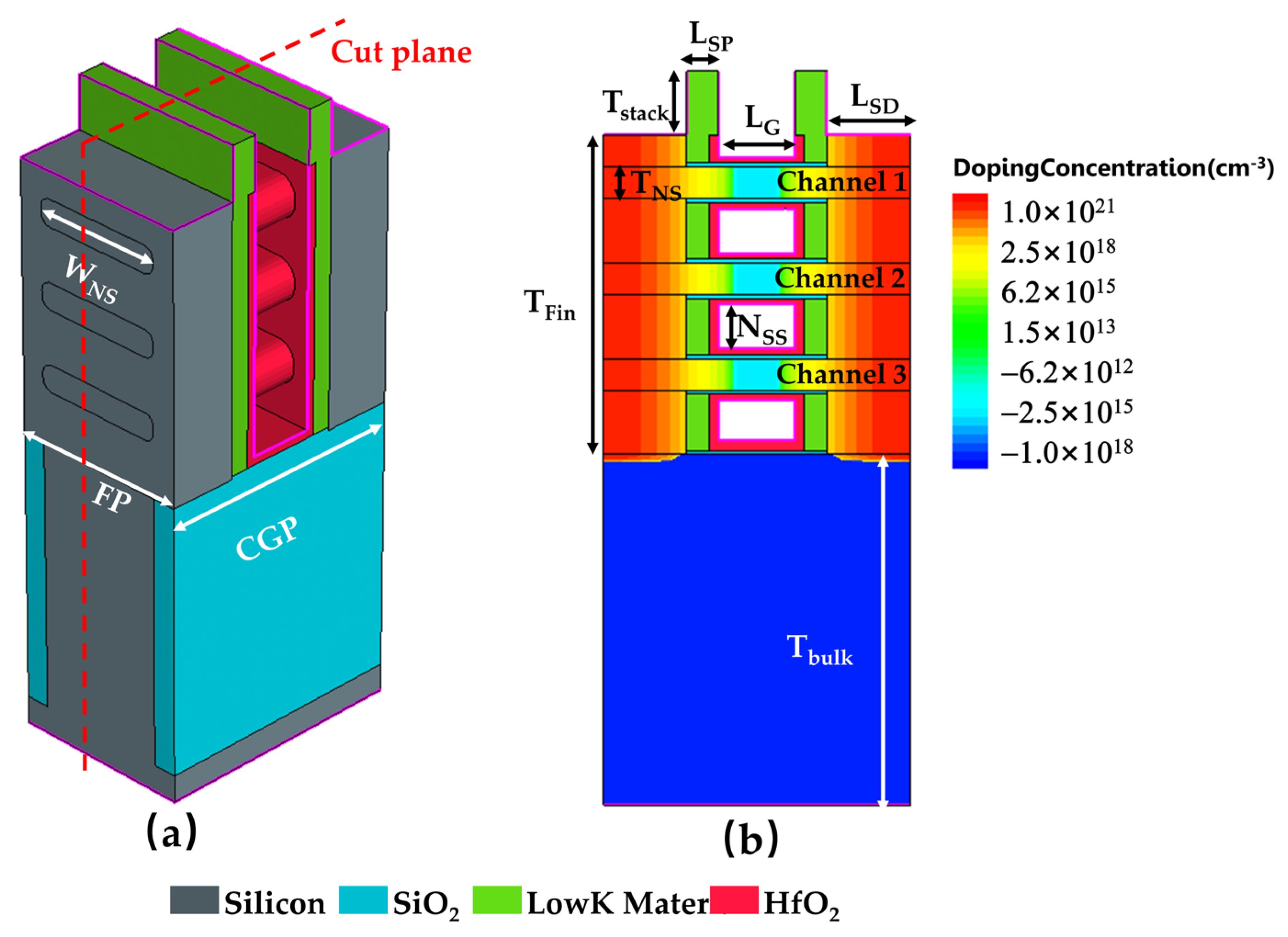
Figure 1. (a) Schematic diagram of device structure. (b) Cross-sectional view along the cut plane.
Electronics 15 00085 g001
Figure 2. (a) Workflow of this work. (b) The Id-Vg curves between simulation results and measured data [16] for 3-stack NSFETs, featuring 5 nm thick nanosheets, a 12 nm gate length. The arrows indicate the curves corresponding to the log scale (left axis) and linear scale (right axis), respectively.
Electronics 15 00085 g002
Figure 3. (a) Transfer characteristics of the device with and without SHE. The black horizontal arrows indicate the curves corresponding to the log scale (left axis) and linear scale (right axis). The red vertical arrow highlights the degradation of the ON-current (Ion) when SHE is considered. (b) Comparison of the simulated SRH recombination rate distributions within the device. The left and right panels show the results without (W/O SHE) and with (W SHE) self-heating effects, respectively. D and S denote the Drain and Source regions, respectively. The purple-red frames indicate the gate oxide regions. D and S denote the Drain and Source regions, respectively.
Electronics 15 00085 g003
Figure 4. (a) Lattice temperature along the cut plane. (b) Heat flux distribution map. (c) Current density along the cut plane. D and S denote the Drain and Source regions, respectively.
Electronics 15 00085 g004
Figure 5. (a) Thermal generation rate distribution along the cut plane. The red dashed box highlights the region of negative thermal generation at the source side. D and S denote the Drain and Source regions, respectively. (b) Energy band distribution along the channel length.
Electronics 15 00085 g005
Figure 6. (a) Temperature variation over time under different gate voltages. (b) Temperature change as a function of gate voltage. The red dots represent the extracted temperature rise values at specific gate bias points.
Electronics 15 00085 g006
Figure 7. (a) Waveforms of the pulsed gate and drain voltages. The blue dashed lines separate the waveform into rise, heating, and cooling regions. (b) The applied gate voltage and the corresponding lattice temperature rise as a function of time. The black and red solid lines represent the pulsed gate bias (Vg) and the resulting thermal response (∆T), respecrively.
Electronics 15 00085 g007
Figure 8. Current density distribution under DC and AC modes.
Electronics 15 00085 g008
Figure 9. (a) Lattice temperature variation curves under fixed cooling time (CT = 2 ps) with varying HT. The red arrow highlights the rise in maximum lattice temperature as the HT extends. (b) Lattice temperature variation curves under fixed heating time (HT = 150 ps) with varying CT. The red arrow illustrates the reduction in final temperature as the CT increases.
Electronics 15 00085 g009
Figure 10. (a) Heavy ion incidence at different positions. The black dashed box outlines the active area where ions are incident at various positions. D and S denote the Drain and Source regions, respectively. (b) Transient current and collected charge at different positions. The black arrows indicate the corresponding Y-axes for the transient current (left) and collected charge (right).
Electronics 15 00085 g010
Figure 11. (a) Incident time of heavy ions. The blue dashed lines separate the waveform into rise, heating, and cooling regions. (b) Transient current and collected charge under conditions with and without self-heating effects.
Electronics 15 00085 g011
Figure 12. Electrostatic potential profile along the channel length before heavy ion incidence, with and without SHE.
Electronics 15 00085 g012
Figure 13. Contours of electric field distribution inside the device before and after heavy ion incidence. D and S denote the Drain and Source regions, respectively.
Electronics 15 00085 g013
Figure 14. Transient drain current and collected charge variations under self-heating conditions and at ambient temperature of 472.7 K. The lattice temperature during heavy-ion incidence under self-heating effects is 472.7 K. The black arrows indicate the corresponding Y-axes for the transient current (left) and collected charge (right).
Electronics 15 00085 g014
Figure 15. (a) Variation in peak drain current and collected charge as a function of heating time. (b) Variation in peak drain current and collected charge as a function of cooling time.
Electronics 15 00085 g015
Disclaimer/Publisher’s Note: The statements, opinions and data contained in all publications are solely those of the individual author(s) and contributor(s) and not of MDPI and/or the editor(s). MDPI and/or the editor(s) disclaim responsibility for any injury to people or property resulting from any ideas, methods, instructions or products referred to in the content.