


Abstract
In an era of rapid technological advancements and growing necessity for effective power management systems, the significance of silicon Metal–Oxide–Semiconductor Field-Effect Transistors (MOSFETs) in contemporary power electronics is more critical than ever. This review explores the advancements in silicon MOSFET technology through the lens of Design Technology Co-Optimization (DTCO). By integrating design and process technology strategies, DTCO optimizes power, performance, area, and cost (PPAC) metrics, addressing the limitations of traditional scaling methods. The manuscript presents an exhaustive analysis of the foundational principles of MOSFET technology, the progression of DTCO, and its implications on critical design metrics. The inclusion of machine learning techniques enhances the DTCO process, enabling vast simulations and efficient design iterations, which are crucial for navigating the complexities of advanced semiconductor device physics. Empirical evidence from TCAD simulations augmented by machine learning insights demonstrates the effectiveness of DTCO in enhancing device performance, reliability, and manufacturing yield. This review emphasizes the significance of DTCO and machine learning in addressing contemporary challenges and influencing the future trajectory of silicon MOSFET technology.
1. Introduction
In an era characterized by rapid advancements in technology and a growing focus on sustainability, the demand for efficient power management systems is increasing [1,2]. As global energy consumption rises and the incorporation of renewable energy sources accelerates, the need for reliable power semiconductor devices becomes increasingly critical [3]. Power semiconductor devices play a crucial role in the operation of modern power electronic systems [4]. They are essential for the conversion of electrical energy in various applications, including renewable energy infrastructures, industrial machinery, and electric transportation systems. These devices also play a key role in regulating and distributing power and energy globally [5].
Similarly, integrated circuits are at the heart of modern digital electronics and computing. Thanks to ongoing advancements in miniaturization, as devices become smaller and more densely packed, the capabilities of integrated circuits have greatly expanded [6]. This progression, often associated with Moore’s Law, reflects the exponential growth in transistor counts and circuit complexity on silicon chips [7]. Since the late 1960s, the number of transistors integrated into each semiconductor chip has experienced a doubling effect approximately every 1.5 to 2 years, resulting in significant enhancements in computational capabilities while concurrently reducing associated costs [8].
The evolution of the semiconductor industry is heavily influenced by two primary technology drivers: dynamic random-access memory (DRAM) and microprocessors [9]. Historically, DRAM technology advanced more rapidly than microprocessors, but from the late 1990s, microprocessors have become equally significant in pushing semiconductor technology forward [10]. For DRAMs, the focus has been on minimizing memory cell area to enhance their density, while microprocessor development emphasizes reducing gate length and increasing the number of interconnect layers [11]. As advancements in transistor miniaturization continue to progress, the scope of semiconductor innovation has expanded significantly. The focus has shifted towards optimizing device performance through innovative approaches like Design Technology Co-Optimization (DTCO) [12]. DTCO integrates design and technology strategies to enhance power, performance, area, and cost (PPAC) metrics, crucial for overcoming the challenges faced by silicon-based Metal–Oxide–Semiconductor Field-Effect Transistor (MOSFETs) [13].
As the semiconductor industry surpasses traditional scaling limits at sub-5 nm nodes, innovations such as ML-assisted compact modeling (MLCM) integrated with TCAD, 2D materials, GAA FETs, high-k/metal gates, and 3D integration—guided by design-technology co-optimization (DTCO)—promise to extend Moore’s Law by boosting device performance, efficiency, and manufacturability, while mitigating challenges like short-channel effects and quantum tunneling (e.g., as demonstrated in TCAD simulations for GAA nanosheet FETs achieving 20–30% RDS(on) reductions; IEEE TED, 2023). While numerous studies have examined DTCO, TCAD, or machine learning in isolation—often for logic devices—none have systematically integrated them for silicon power MOSFET optimization. This review uniquely fuses device physics, process technology, and data-driven modeling into a unified DTCO–ML framework to enhance key metrics like RDS(on), breakdown voltage, and switching efficiency. Unlike conventional descriptive reviews, it delivers a critical comparative analysis of methodologies, exposing limitations (e.g., MLCM’s data scarcity issues in high-voltage regimes), implementation hurdles, and cross-domain synergies. It also charts future pathways for extending DTCO–ML to wide-bandgap materials (GaN, SiC) and architectures like GAA-FETs, providing actionable insights from academic and industrial lenses to accelerate next-generation power semiconductor design (inspired by hybrid ML-TCAD workflows in Nature Electronics, 2024, showing 15% switching loss improvements).
2. Fundamentals of Power MOSFETs
2.1. Background
A MOSFET constitutes a specific category of transistor that is employed for the purposes of amplifying or switching electronic signals. This device serves as a crucial element within integrated circuits (ICs), finding extensive application across both analog and digital domains [14]. The operational mechanism of a MOSFET involves regulating the movement of charge carriers (either electrons or holes) through a semiconductor channel, with this flow being modulated by a voltage that is applied to the Gate (G) terminal [15]. The foundational concept of field-effect transistors was first introduced in 1925 with a corresponding United States patent submitted by Julius Edgar [16]. Nevertheless, the actual invention of MOSFETs is attributed to Dawon Kahng and Martin Atalla, who conducted their pioneering work at Bell Laboratories during the late 1950s [17]. In the initial stages, the gate material utilized in these transistors predominantly consisted of metals such as aluminum, which ultimately resulted in the nomenclature “Metal Oxide Semiconductor” for these types of devices [18]. Subsequently, heavily doped polycrystalline silicon (poly-Si) emerged as the standard gate material owing to its superior thermal stability and its non-reactivity with the gate oxide [19]. In contemporary research investigations, there has been a resurgence in the utilization of metal gate materials, particularly in scenarios where silicon dioxide (SiO2) gate oxide has been replaced with advanced high-k dielectrics [20]. The inaugural commercial announcement of ICs predicated on MOS technology was made by General Microelectronics in 1964 [17]. Despite this huge advancement in technology, it took nearly a decade to address the fundamental yield and reliability challenges, thereby enabling MOS technology as the predominant component in IC technology.
2.2. Overview of MOSFET
Apart from the substrate body terminal (B), a MOSFET mainly consists of three terminals: gate (G), source (S), and drain (D). The body terminal may be interconnected with the source, thus yielding a three-terminal configuration [21]. The fundamental architecture of a MOSFET encompasses an S and D region, which are extensively doped to pentavalent n-type or trivalent p-type semiconductor, alongside a G-terminal that is insulated from the channel by a layer of SiO2. The material used for the gate can either be metallic or heavily doped polycrystalline silicon [22]. The channel region is situated between S and D and is modulated by the voltage applied to the G-terminal. Depending on their structure, MOSFETs can be classified as n-channel (nMOS) or p-channel (pMOS). In the former, electrons serve as the charge carriers while the body is doped with p-type impurities. Conversely, in pMOS transistors, holes are the charge carriers with the body being n-type doped. This classification of MOSFETs is illustrated in Figure 1a. The synergistic integration of nMOS and pMOS transistors in a complementary arrangement is referred to as CMOS (Complementary Metal–Oxide–Semiconductor) technology, which exhibits high efficiency in switching applications characterized by minimal power dissipation [23]. In contemporary MOSFET configurations such as FinFETs, the channel manifests as a slender fin of silicon that ascends vertically from the substrate, thereby enhancing control over the channel and mitigating short-channel effects [24]. The structural representation of a MOSFET is depicted in Figure 1b.
Figure 1.
(a) Classification of MOSFET and (b) cross-section of 2D planar MOSFET.
2.3. Operation of MOSFET
The working of MOSFET is based on the charge carriers within the channel region. Upon the application of voltage to the G-terminal, an electric field is generated that exerts influence over the charge carriers within the channel [25]. In the context of an nMOS transistor, a positive G-voltage serves to attract electrons towards the channel, thereby establishing a conductive pathway between the S and D. In contrast, a negative gate voltage in a pMOS transistor draws holes into the channel. The operational behavior of the MOSFET varies across distinct modes contingent upon the G-voltage: accumulation, depletion, and inversion. In the accumulation mode, when the G-voltage is lower than the threshold voltage (VTH), the channel remains non-conductive, positioning the MOSFET in the ‘off’ state. As the gate voltage is progressively increased, it leads to the depletion of charge carriers in the channel, thereby diminishing the channel’s conductivity, a phenomenon referred to as the depletion mode. For G-voltage higher than VTH, the channel switches to a conductive state, and the MOSFET moves to its ‘on’ state (inversion mode) [26]. When the drain voltage (VD) is high enough to cause the channel to pinch off near the drain, resulting in a constant current (ID) despite further increases in VD, it is called saturation mode. Figure 2 illustrates all these different operational modes in its four panels: (a) accumulation, (b) depletion, (c) inversion, and (d) saturation.
Figure 2.
Operation modes for a MOSFET: (a) accumulation, (b) depletion, (c) inversion, and (d) saturation. Figure reused with permission from MKS Inc. (2017). Figure 13 of: Operating characteristics of an NMOS field-effect transistor. MKS Handbook, Semiconductor Devices and Process Technology by the Office of the CTO. www.mks.com.
Several pivotal characteristics delineate the performance metrics of MOSFETs. VTH denotes the minimal G to S voltage necessary to establish a conductive pathway between the S and D. The on-resistance (RDS(on)) represents the resistance encountered between the D and S terminals when the MOSFET is operating in the ‘on’ state, thereby impacting power dissipation and efficiency. The cumulative charge needed for toggling the MOSFET between its on and off states is the gate charge (Qg), which therefore affects the MOSFET switching speed and overall efficiency. The breakdown voltage (VBD) instead represents the maximum D to S voltage that the MOSFET is able to sustain without experiencing failure. All these characteristics are essential for assessing the suitability of a given MOSFET for a proper application, especially in the field of power electronics, where efficiency and reliability are of utmost importance. Figure 3 illustrates the key developments, highlighting the progression from basic research to mass production over the years. This timeline shows the continuous efforts to enhance the performance, efficiency, and scalability of silicon MOSFETs.
Figure 3.
Evolution of MOSFET and advancements over the years.
2.4. Scaling of MOSFETs
Scaling constitutes a pivotal methodology for attaining faster and more compact integration of devices, which is imperative for the prosperity of the VLSI sector. The process of device scaling augments packing density, enhances circuit speed, and mitigates power dissipation. The fundamental concept of scaling entails a reduction in the overall dimensions of transistors while preserving their operational efficacy [27]. In the initial stages, MOSFET G-lengths were quantified in micrometers; however, they have now transitioned to the nanoscale. For instance, the smallest MOSFETs that were produced as of 2019 comprise the 5 nm FinFET semiconductor nodes, fabricated by Samsung Electronics and TSMC [28,29]. Scaling facilitates improvements in processing velocity and radio frequency (RF) performance. RF MOSFET circuits, specifically designed for high-frequency applications, experience advantages from elevated cut-off frequencies, which can attain values as high as 400 GHz through the minimization of device dimensions [30]. The progressive advancement in MOSFET gate scaling technology is exemplified in Figure 4, which indicates the main milestones since 1974, when the reduction in MOSFET channel length was driven by Dennard scaling, suggesting that transistor dimensions should scale proportionally to improve efficiency [31]. This approach explained the consistent reduction in channel length over time, though short-channel effects soon became a challenge until, in the 1980s and 1990s, multi-gate designs like the double-gate MOSFET were proposed to combat these effects, improving control over the channel [32]. This led to the introduction of the FinFET in 1999, a double-gate structure with a “fin” design that significantly enhanced channel control, enabling scaling down to 20 nm nodes while mitigating short-channel effects [33]. In 2007, high-k dielectrics and metal gates were introduced, crucial for continuing scaling at the 45 nm node and beyond by reducing leakage currents. This marked a turning point in overcoming the limitations of traditional silicon dioxide and polysilicon gates [34]. By 2011, Intel’s Tri-Gate transistors at 22 nm pushed the boundaries further, using a 3D design with three gates for improved channel control and energy efficiency [35]. This transition to 3D transistors was a major leap in overcoming the limitations of planar designs.
Figure 4.
Year-wise gate length reduction in VLSI technology, highlighting the main milestones. See main text for more details.
There exist two predominant scaling mechanisms: Constant Voltage Scaling and Constant Field Scaling. In the context of Constant Field Scaling, all dimensions and voltages are proportionally reduced by a factor of ‘α’, while simultaneously increasing doping and charge densities by the same factor. This approach preserves the electric field within the transistor, resulting in an enhancement of circuit speed by a factor of ‘α’ and circuit density by a factor of α2. Conversely, Constant Voltage Scaling entails a reduction in all MOSFET dimensions by a factor of ‘α’, apart from terminal voltage and power supply [30]. Nonetheless, this can precipitate reliability challenges, such as oxide breakdown, electrical overstress, and electromigration. Constant Field Scaling is typically favored due to its ability to scale all terminal voltages and power supplies uniformly in conjunction with dimensions, as opposed to Constant Voltage Scaling. However, a reduction in voltages is not invariably practicable, as peripheral and interface circuits may necessitate fixed voltage levels for both input and output. This requirement engenders the need for multiple power supply voltages and intricate level-shifting strategies. For the implications of scaling mechanisms on a variety of parameters, see Table 2 of Ref. [30].
2.5. Challenges in Scaling and Performance
Silicon MOSFETs find extensive applications in numerous power electronic systems because of their excellent efficiency, rapid switching abilities, and durability. Common applications include switching power supplies, motor drives, inverters, and amplifiers. In switching power supplies, MOSFETs are used in DC-DC converters and AC-DC power supplies for efficient power conversion. In motor drives, they control the speed and torque of electric motors in industrial and automotive applications. Inverters utilize MOSFETs to convert DC to AC power in renewable energy systems, such as solar inverters and uninterruptible power supplies. Furthermore, MOSFETs are highly used in audio and RF amplifiers for signal amplification with scarce distortion. However, as power MOSFETs are scaled down to achieve higher performance and efficiency, several challenges arise because smaller devices generate more heat, requiring advanced cooling techniques to prevent thermal runaway and ensure reliability. Techniques such as microfluidic cooling, which uses microchannels for efficient heat dissipation, and advanced thermal interface materials that improve thermal conductivity between the MOSFET and the heat sink are being explored. Reduced dimensions lead to increased parasitic resistances and capacitances affecting switching speed and efficiency [36]. Maintaining high breakdown voltage while concurrently minimizing the dimensions of the MOSFET presents a formidable challenge, thereby necessitating sophisticated material engineering and innovative design methodologies. Phenomena such as drain-induced barrier lowering (DIBL) and leakage currents become increasingly pronounced as MOSFETs undergo miniaturization. Cutting-edge transistor architectures, including FinFETs and multi-gate transistors, facilitate enhanced control over the channel and mitigate short-channel effects. Furthermore, techniques in strain engineering, which involve inducing strain within the silicon lattice to enhance carrier mobility and reduce leakage currents, are currently being implemented. According to the International Technology Roadmap for Semiconductors, the overarching objective is the reduction in CMOS dimensions. Nonetheless, the traditional planar CMOS device is nearing the threshold of scalability, prompting the exploration of alternative device configurations. While the miniaturization of transistors yields benefits such as area efficiency, augmented speed, and improved performance, it simultaneously engenders substantial complications, particularly at the nanometer scale. As MOSFETs are subjected to scaling, the inter-transistor barrier diminishes, thereby amplifying the probability of quantum tunneling, wherein carriers migrate between transistors. This phenomenon is intricately associated with the thickness of the oxide layer. The decrease in oxide thickness has a direct impact on gate current because of carrier tunneling through the insulator’s potential barrier. As the barrier distance diminishes, the tunneling effect escalates exponentially. Thin gate insulators are instrumental in regulating channel potential, thereby circumventing short-channel effects induced by the drain electric field’s encroachment into the channel. However, two primary constraints arise from oxide thickness: the narrowing of oxide layers exacerbates leakage current, which is particularly pronounced in standby mode, alongside the loss of inversion charge and transconductance stemming from polysilicon gate depletion and inversion-layer quantization effects [37,38,39]. The threshold voltage does not decrease in direct proportion to transistor scaling, resulting in elevated leakage currents. When the channel length falls below 0.1 μm, the threshold voltage current does not instantaneously reach zero but instead diminishes exponentially, being influenced by thermal energy. This culminates in leakage current, which is critical to minimizing power loss. Consequently, transistors must be engineered with exceedingly low threshold voltages [40]. The evolution of silicon MOSFET scaling has been marked by significant milestones and advancements over the years. Figure 5 illustrates the key developments in the field, highlighting the progression from geometric to 3D integration scaling. Present-day MOSFET designs encounter constraints when the channel length approaches approximately 30 nm due to Zener breakdown at the source/substrate junction and gate leakage phenomena. It becomes increasingly intricate to maintain control over the channel and leakage current at the gate [38,40]. As dimensions contract, short-channel effects predominantly influence device performance, leading to challenges such as high leakage and performance degradation. Within the nanoscale domain, the imperative to mitigate short-channel effects while preserving device efficacy constitutes a significant hurdle. Diverse strategies to mitigate the short-channel effects frequently entail adverse consequences, including augmented leakage and performance decline. In addition to electrical and thermal challenges, warpage control has emerged as a critical issue in the scaling of silicon MOSFETs, particularly in Trench Field-Plate (FP) MOSFETs. As device structures become more complex, mechanical stress induced by deep trenches, thick oxide layers, and metallization processes leads to wafer deformation, affecting alignment accuracy and increasing the likelihood of defects during fabrication. Warpage is especially problematic in high-density power devices where stress imbalance can result in handling errors, compromised device integrity, and reduced manufacturing yield. Studies have shown that trench angle variations and FP oxidation significantly contribute to warpage, making it a crucial factor to consider in MOSFET design and process optimization [41]. To address these challenges and continue the advancement of MOSFET technology, innovative approaches are required. One such approach is DTCO, which integrates design and technology strategies to enhance PPAC metrics. DTCO has emerged as a crucial methodology for overcoming the limitations of traditional scaling methods and ensuring the continued relevance and performance of MOSFETs in modern power electronics [42]. The following section will provide an overview of DTCO, its objectives, and its historical evolution, highlighting its significance in the development of advanced semiconductor devices.
Figure 5.
Progression of MOSFETs from geometric to 3D integration scaling.
3. Overview of DTCO
DTCO is a strategic methodology in semiconductor engineering that aligns design and process technology development to optimize PPAC metrics [43]. DTCO has emerged as an essential approach to managing the increasing complexity of semiconductor manufacturing, also due to the physical and economic limits of conventional scaling approaches. The early and continuous collaboration between design teams and foundries ensures that advancements in design and process technology complement each other, allowing them to achieve optimal results. Historically, the semiconductor industry relied on Moore’s Law, which predicted the doubling of transistors on a chip approximately every two years, to drive exponential improvements in performance and cost. However, as technology nodes approach the nm scale, issues such as quantum tunneling, short-channel effects, and thermal management have made traditional scaling increasingly challenging. This has necessitated the adoption of DTCO, first referenced in 2005, as a comprehensive strategy to bridge the gap between design choices and process constraints [44].
The primary objectives of DTCO include reducing power consumption, enhancing energy efficiency, increasing processing speed, reducing latency, maximizing transistor density, and reducing manufacturing costs, all while maintaining or improving device performance and reliability. DTCO’s success hinges on the collaborative approach between design and process technology teams from the earliest stages of technological development. This collaboration ensures that design choices are tailored for the manufacturing process and vice versa, creating a harmonious development cycle where advancements in one area enhance the other. A key component in this integration is the use of Technology Computer-Aided Design (TCAD) tools, which provide detailed simulations of semiconductor devices, considering variables such as doping profiles, material characteristics, and geometric structures [45]. TCAD modeling helps predict device performance and reliability under different conditions. Furthermore, it assists in optimizing fabrication steps like ion implantation, diffusion, etching to understand their impact on device yield and efficiency. TCAD models, often integrated with SPICE (Simulation Program with Integrated Circuit Emphasis), enable comprehensive circuit-level simulations, allowing designers to assess how device-level changes affect the overall circuit performance [46]. A generalized DTCO flow is shown in Figure 6.
Figure 6.
Design technology co-optimization flow. Figure adapted from Ref. [47] under the terms of the Creative Commons Attribution 4.0 International license.
Recent advancements in machine learning (ML) have further enhanced TCAD by enabling more vast and efficient simulations, thus reducing the dependence on extensive physical testing [48,49,50]. ML algorithms possess the capability to scrutinize extensive datasets derived from simulations in order to discern patterns and enhance device parameters with greater efficacy than conventional methodologies. This integration offers significant benefits, including improved device performance, enhanced reliability, cost-effective manufacturing, and faster time-to-market [48,49,50]. For instance, neural networks can be trained on TCAD simulation data to predict key performance metrics such as on-resistance, switching speed, and leakage currents. Taking advantage of simulations, designers can promptly address potential reliability issues, reinforcing DTCO’s role in developing high-efficiency semiconductor devices [51]. Furthermore, the inclusion of ML algorithms into the DTCO framework represents a significant step forward in the evolution of semiconductor technology since this would allow the semiconductor industry to leverage advanced data analytics for pushing the boundaries of device performance and manufacturing efficiency.
In practical DTCO implementations, TCAD outputs are typically post-processed into structured datasets in which each simulated device instance is represented by a set of process and design parameters (such as channel geometry, doping conditions, bias, and temperature) together with electrical figures of merit, including on-resistance, threshold voltage, breakdown voltage, and leakage current. These tabulated datasets, commonly exported in formats such as CSV or SQL, are then used to train supervised ML models that map design and process knobs to device-level performance metrics. To build reliable surrogates, modern TCAD-enabled ML frameworks often automate data generation through a design-of-experiments strategy that distributes simulation points across the multi-dimensional process and design space, ensuring that the training set is sufficiently rich for accurate modeling. To reduce extrapolation errors at extreme operating points (for example, high temperature, high voltage, or aggressively scaled geometries), the design space is further extended with corner and guard-band simulations so that the training distribution spans a wide and representative region of the technology space. Complementary to this, recent DTCO–ML workflows incorporate uncertainty estimation and out-of-distribution detection, so that candidate designs falling outside the trusted region of the surrogate are flagged for additional TCAD simulations and subsequent model retraining, effectively creating an iterative, closed-loop refinement of the ML model and improving its robustness in extreme parameter spaces.
3.1. Evolution of DTCO
The evolution of DTCO from a fab-centric process to a multi-lateral, integrated approach has been driven by the increasing complexity of semiconductor manufacturing. In earlier technology nodes, such as those around the 90 nm mark, the semiconductor industry relied on a straightforward model where foundries provided Process Design Kits (PDKs) containing design rules and transistor models, and designers created products within those predefined constraints. However, as technology nodes advanced to 65 nm and below, new challenges emerged, including yield concerns and limitations posed by sub-wavelength lithography. This period marked the beginning of Design for Manufacturability (DFM) and necessitated the move toward more restrictive design rules.
As technology transitioned below 28 nm, challenges such as double patterning and the adoption of FinFETs introduced significant complexity that required early and continuous collaboration between fabs and design teams. The introduction of FinFETs at nodes below 20 nm further demanded a paradigm shift in standard cell design, emphasizing the need to adapt discrete device widths and fit a specific number of fins within each cell [52]. These advancements reinforced the importance of early collaboration between process technology developers and designers to ensure optimized scaling. Looking ahead, DTCO is set to evolve further with the integration of new transistor architectures such as Quantum Well FETs (QWFETs), horizontal and vertical nanowires (HNW, VNW), and 2D semiconductors, along with carbon nanotubes (CNTs). The development of advanced lithography techniques, including self-aligned double patterning (SADP) and Extreme Ultraviolet (EUV) lithography, will continue to support tighter scaling but also introduce trade-offs related to complexity and cost. Additionally, 3D Integrated Circuits (3D ICs) will open up new scaling opportunities by restructuring logic and memory integration within a single chip. As these innovations progress, DTCO will remain vital in addressing reliability concerns such as Bias Temperature Instability (BTI), Time-Dependent Dielectric Breakdown (TDDB), and Electromigration (EM) [53].
3.2. TCAD Models: Historical Development and Modern Advancements
TCAD has developed significantly over the past seventy years, becoming an essential tool in semiconductor device design and optimization. Through the utilization of TCAD-to-SPICE methodologies, parameters that are contingent upon technology pertaining to device models are derived from TCAD outputs, subsequently being integrated into the circuit simulation environment. For executing a realistic evaluation of the specified integrated circuit technology within the electronic computer-aided design (ECAD) framework, it is imperative to incorporate into the TCAD simulation process’s numerous critical reliability factors, including parasitic effects, hot carrier degradation (HCD), quantum phenomena, BTI, gate leakage, and kink phenomena. Consequently, a proficient TCAD-to-SPICE model functions as the bridge connecting advanced technological paradigms with IC design, encompassing aspects such as device geometry, bias voltage, temperature, DC, AC, RF, and so on.
The evolution of TCAD models began with the foundational PN theory analysis in 1949 and progressed with significant advances in the 1960s when Bell Labs and IBM conducted simulations for diode devices [54]. A major milestone was reached in 1964 when Gummel introduced a self-consistent iterative method for one-dimensional transistor simulation, laying the groundwork for the Gummel–Poon model for bipolar transistors in 1970. This model improved simulation accuracy by incorporating detailed charge control relations, essential for precise current calculations. As semiconductor devices advanced, one-dimensional models became insufficient, especially for handling the complexities of modern scaled-down devices [55]. This led to the development of multi-dimensional simulation tools. P. Cottrell and E. Buturla’s finite element analysis method, introduced in 1975, enabled more robust multi-dimensional simulations [56]. The development of MINIMOS by Siegfried Selberherr marked a significant leap, providing two-dimensional simulations of FETs that helped address short-channel effects as devices were scaled down [57]. Subsequent versions, like MINIMOS-5 and MINIMOS-6, expanded the modeling to three-dimensional capabilities. Additionally, M.R. Pinto’s PISCES IIB offered comprehensive multi-dimensional device simulations, allowing for optimized doping profiles and better handling of short-channel effects [58]. The SUPREM series by D.A. Antoniadis further enhanced process simulation, establishing TCAD as a crucial tool for understanding complex device behavior [59,60]. The progression of TCAD in drift-diffusion and Boltzmann equations is illustrated in Figure 7. Traditional TCAD compact models were developed to represent the physics of semiconductor devices, each with its unique approach. The Pao-Sah model (1966) was a foundational surface potential-based model that defined the drain-source current using drift and diffusion mechanisms [61]:
with W being the channel width, μ the carrier mobility, Qi the inversion charge density, Vc the channel potential, and dy an infinitesimal element along the channel length direction (y-axis), from source (y = 0) to drain (y = L). So, Equation (1) derives the drain current as drift current through differential channel segment dy, where dVc/dy is the channel potential gradient (electric field) along the channel length. This model, while accurate, required complex numerical solutions due to its iterative nature.
Figure 7.
Evolution of TCAD over 70 years. Figure reproduced from Ref. [60] under the terms of the CC BY license. For more information and full references details see the original paper.
On the other hand, threshold voltage-based models simplified computations by defining VTH as the boundary between operational modes, useful for practical circuit simulations [62]. The Berkeley Short-channel IGFET Model (BSIM) introduced in 1987 was significant in addressing short-channel effects and evolving through versions like BSIM2 and BSIM3 [63,64]. The basic equation for threshold voltage-based models is
Here, is drain-source current (A), µ is the carrier mobility in a channel of width W and length L; C is the capacitance per unit area of gate, is gate-source voltage, is threshold voltage, is gate-drain voltage and l is a channel-length modulation constant. Similarly, surface potential-based models such as the Hiroshima-University STARC IGFET Model (HiSIM) retained more detailed physics information by focusing on the surface potential ϕs [65]. A representative equation for surface potential-based models, in terms of analytical surface potential at the end of channel (i.e., Drain-terminal ϕsD or Source-terminal ϕsS) and of the Flat-Band voltage (VFB) and of the Thermal voltage VT, is [60,66]
Despite their significant contributions, traditional TCAD models face challenges as semiconductor devices scale down to nm dimensions. As already mentioned, quantum effects such as tunneling and confinement complicate device behavior and often require modifying conventional models. The reliance on non-physical parameters for empirical fitting further complicates model accuracy and increases computational demands. To bridge these limitations, modern TCAD integrates ML techniques to enhance simulation accuracy and reduce computational costs. ML-assisted compact models (MLCMs) leverage neural networks and data-driven techniques to improve the predictive power of simulations, making them more efficient [49]. Hybrid approaches that combine physical models with ML ensure that the simulations remain grounded in theoretical rigor while benefiting from the flexibility and speed of data-driven insights. These advanced methodologies have proven effective in simplifying quantum transport equations, essential for simulating modern transistors like FinFETs and gate-all-around (GAA) FETs, addressing both the precision and efficiency challenges faced by traditional TCAD models.
3.3. Machine Learning Fundamentals for Semiconductor Design
ML has emerged as an integral component of modern semiconductor design, providing powerful data-driven tools for modeling, optimization, and automation across multiple abstraction levels. As semiconductor technologies advance toward deeply scaled and heterogeneous architectures, conventional physics-based TCAD simulations face escalating computational demands, making ML surrogates essential for dramatically reducing design cycle times from weeks to hours while managing device complexity, nonlinearity, and variability [67]. ML techniques learn complex relationships directly from simulation data, improving design efficiency, scalability, and predictive accuracy. In semiconductor design workflows, ML has found widespread application in areas ranging from analog and mixed-signal circuit design to device-level modeling and physical design optimization. By enabling fast surrogate modeling, automated optimization, and intelligent decision-making, ML complements traditional TCAD and design methodologies and has become a key enabler for next-generation DTCO frameworks [68].
From a methodological perspective, ML techniques applied in semiconductor design can be broadly categorized into supervised, unsupervised, and reinforcement learning. Supervised learning dominates semiconductor applications, where labeled datasets from TCAD, SPICE, or silicon measurements are used to build regression and classification models that predict key figures of merit such as IDS, VTH, leakage current, and breakdown voltage from process and layout parameters. These models are widely adopted in DTCO for surrogate modeling, variability-aware compact model generation, and performance–power–area trade-off analysis across large design spaces [69]. In contrast, unsupervised learning focuses on discovering structure in unlabeled data, and is particularly effective for clustering wafer defect patterns, monitoring process drifts, and extracting latent variability modes from inline metrology or electrical test data. Techniques such as clustering and dimensionality reduction help engineers identify outliers, yield limiters, and systematic process signatures that are difficult to detect with manual analysis. Reinforcement learning, though more recent in semiconductor design, targets sequential decision-making problems such as design-space exploration, floor-planning, and placement–routing optimization, where an agent learns policies to maximize reward functions related to timing, power, congestion, or yield. Together, supervised, unsupervised, and reinforcement learning form a complementary ML ecosystem that supports predictive modeling, anomaly detection, and automated optimization in modern semiconductor workflows [70].
In addition to learning paradigms, selecting appropriate ML algorithms critically influences semiconductor process and device optimization, as each model family offers distinct trade-offs in accuracy, interpretability, data requirements, and computational runtime across design workflows. Supervised algorithms dominate practical applications: kernel ridge regression (KRR) and support vector regression (SVR) excel with small datasets (<5000 samples) for nonlinear mapping of TCAD parameters; tree ensembles including random forest (RF) for feature importance ranking, extreme gradient boosting (XGBoost), light gradient boosting machine (LightGBM), and gradient boosted decision trees (GBDT) are preferred for virtual metrology, yield prediction, and fault diagnosis due to their robustness and built-in interpretability; while artificial neural networks (ANNs), convolutional neural networks (CNNs), and deep neural networks (DNNs) capture complex nonlinear relationships in spectral/imaging/multi-parameter TCAD data, routinely delivering 100–1,000,000× speedups versus physics-based simulations. Complementing these, unsupervised algorithms such as k-means and density-based spatial clustering of applications with noise (DBSCAN) enable wafer defect pattern discovery and clustering, while principal component analysis (PCA), t-distributed stochastic neighbor embedding (t-SNE), and autoencoders extract latent variability modes and detect anomalies from high-dimensional optical emission spectroscopy (OES)/ellipsometry streams. Reinforcement learning (RL) and evolutionary strategies further extend capabilities to sequential/multi-objective problems like design-space exploration and advanced process control tuning under simultaneous power–performance–area–yield constraints [71]. Table 1 summarizes these techniques’ strengths, limitations, and applications.
Table 1.
ML Algorithms for Semiconductor Process Optimization. Different algorithms offer complementary strengths, with selection guided by problem complexity, data availability, and computational constraints. Neural networks (ANNs) excel at modeling complex nonlinear physics (MSE < 0.01, R2 = 99%) but require large datasets and extensive training. Tree-based methods like LightGBM provide superior interpretability, handle sparse/mixed data effectively, and achieve <1% prediction error, ideal for rapid design exploration. Multi-layer NNs deliver high accuracy for statistical device variation (MSE = 4.32 mV2) at higher training costs.
4. DTCO for Silicon MOSFETs
DTCO has become a critical methodology in enhancing the performance and efficiency of silicon MOSFETs, impacting various key design parameters such as gate length and width, VTH, on-resistance, gate charge (Qg), and breakdown voltage (VBD). The integration of TCAD simulations within DTCO plays a fundamental role in fine-tuning these parameters to achieve optimal device performance [72]. Through TCAD simulations, engineers can optimize the gate length and width to enhance switching speeds and reduce on-resistance, which are crucial for efficient power conversion. Similarly, adjusting the threshold voltage helps maintain ideal switching characteristics, thereby reducing power loss during transitions. Minimizing gate charge is very important because it directly contributes to faster switching speeds and improves overall efficiency. A high breakdown voltage value is also critical for sustaining reliability under high-stress conditions, which is essential in power electronics applications. DTCO both focuses on enhancing performance metrics and addresses reliability and manufacturing yield, with the aim to ensuring long-term device functionality and cost-effectiveness.
To mitigate reliability issues such as electromigration, hot carrier injection, and bias temperature instability, DTCO includes the careful selection of materials and process optimizations together with the use of electromigration-resistant interconnects and advanced stress-testing protocols to ensure that devices can withstand high operational stress over extended periods. Improving manufacturing yield is equally significant, and DTCO approaches this through defect reduction strategies and the implementation of robust design rules that minimize the effects of process variations. By focusing on these aspects, DTCO facilitates the development of reliable, cost-effective, and high-performance MOSFETs. Empirical evidence supports the benefits of DTCO in real-world applications. For example, TCAD simulations have proven effective in optimizing gate dimensions, achieving lower RDS(on) and faster switching speeds. The adoption of FinFET structures as part of DTCO strategies has shown substantial power savings and performance gains, as FinFETs provide superior control over the channel and mitigate short-channel effects. Other studies have demonstrated how DTCO can reduce manufacturing costs and improve yield by employing stringent design rules and defect minimization techniques [73]. These real-world examples underscore the pivotal role of DTCO in modern power electronics, demonstrating its capability to align design and manufacturing processes for enhanced device performance and reliability.
5. Empirical Evidence of DTCO in Enhancing MOSFET Performance
The practical application of DTCO in silicon MOSFETs is supported by various studies that utilize TCAD simulations to optimize key device parameters, showcasing its profound impact on advancing semiconductor technology. To build on a comprehensive background and theoretical discussions, this section highlights notable examples from the literature, emphasizing the improvements achieved in PPAC through DTCO approaches. Numerous studies have demonstrated how TCAD modeling integrated with DTCO is essential for analyzing and fine-tuning the electrical characteristics of MOSFETs. For instance, simulation-based investigations have shown how optimizing gate dimensions significantly reduces on-resistance (RDS(on)) and enhances switching speed, key metrics for power conversion efficiency. This finding is consistent across various studies that applied TCAD to model the effects of scaling down channel lengths while addressing short-channel effects such as drain-induced barrier lowering (DIBL) and gate leakage. For instance, Saadat et al. conducted an in-depth study focusing on the optimization of channel lengths for planar Laterally Diffused Metal–Oxide–Semiconductor (LDMOS) Field-Effect Transistors (FETs) aimed at low-voltage power applications, illustrated in Figure 8 [74]. The primary objective was to identify an optimal channel length that minimizes the specific on-resistance while maintaining adequate device performance for low-voltage operations, particularly at 3.3 V and 5 V. The study employed TCAD simulations to model n-channel LDMOS transistors with Gaussian doping profiles for various regions, such as the source, drain, p-body, and drift.
Figure 8.
Planar Laterally Diffused Metal–Oxide–Semiconductor. Figure reproduced from Ref. [74] under the terms of the CC BY license.
An automated code iteratively optimized the drift region length and body doping concentration to achieve a target leakage current of 10−13 A/µm, a critical aspect for ensuring low off-state power dissipation as depicted in Figure 9a,b.
Figure 9.
Transfer characteristics of 5 V LDMOS devices (a) All devices have a fixed leakage current, 10−13 A/μm (b) for devices before applying optimization algorithm. Figure reproduced from Ref. [74] under the terms of the CC BY license.
The results indicate that an optimal channel length of approximately 40 nm minimized specific on-resistance for both voltage levels, as shown in Figure 10. Below this length, an increase in on-resistance was observed due to significant electron mobility degradation, mainly caused by enhanced impurity scattering from higher doping levels.
Figure 10.
Optimal channel length of LDMOS. Figure reproduced from Ref. [74] under the terms of the CC BY license.
The authors noted that electron mobility dropped rapidly for shorter channel lengths, as increased p-body doping to control leakage current introduced higher impurity scattering Figure 11. This optimal channel length for LDMOS was found to be slightly longer than that of conventional planar CMOS transistors due to stricter leakage current requirements in power applications [74].
Figure 11.
Electron mobility and threshold voltage for 5V LDMOS devices. Figure reproduced from Ref. [74] under the terms of the CC BY license.
In another study, Nawaz et al. demonstrated through 3D TCAD simulations that optimizing fin geometry and doping profiles in 30 nm SOI-based MuGFETs significantly improved device performance metrics such as on-current and transconductance, without adversely impacting threshold voltage or short-channel effects. Additionally, the study underscored the importance of fin width control to minimize DIBL, subthreshold slope, and off current, confirming TCAD’s effectiveness for predictive modeling and validation with experimental results. Fine-tuning process parameters like dopant diffusion and implant tilt was also found to enhance leakage control, showcasing TCAD’s pivotal role in refining sub-100 nm device behavior [75].
Similarly, Tsague et al. focused on optimizing polysilicon gate biaxially strained silicon MOSFETs using TCAD simulations, highlighting the potential for performance enhancement through strain engineering. Utilizing Silvaco’s Athena for process simulation and ATLAS for device characterization, they showcased the impact of biaxial strain on improving carrier mobility and overall device behavior. The findings indicated that biaxial strain increased electron mobility by approximately 35.7%, resulting in a higher drain current and better current drive capabilities. This enhancement also led to improved sub-threshold characteristics and controlled leakage current, making the devices more suitable for low-power applications [76]. Likewise, Cadareanu and Gaillardon demonstrated through TCAD simulations that Three-Independent-GateField-EffectTransistors (TIGFETs) at the 10 nm node showcased impressive on-current values, reaching 115.63 μA/μm for n-type and 108.02 μA/μm for p-type transistors under a 0.7 V supply voltage. This positions TIGFETs as a competitive alternative to contemporary FinFETs. The use of silicon–germanium channels further boosted current drive by approximately 8×compared with silicon alone, illustrating the benefits of mixed-material channel strategies [77].
Pal et al. focused on the design and optimization of Tunnel FETs using TCAD simulations, highlighting the challenges and improvements in circuit performance compared with conventional CMOS devices [78]. The work emphasized how TFETs, despite their promising low subthreshold swing and low OFF-current, face limitations such as higher gate capacitance and a unique drain-barrier voltage that affects rise/fall times and overall speed. The TCAD simulations demonstrated that optimizing device parameters, such as ON-current (ION), saturation voltage (VDSAT), and drain-barrier voltage (VDTH), can lead to significant improvements in propagation delay and fall time. For instance, the study showed that decreasing VDSAT reduced propagation delay, enabling a more balanced trade-off between delay and power dissipation in TFET circuits. The relationship between propagation delay and ION and the impact of VDSAT on fall time was notable in the study. These findings underline the potential of advanced TCAD modeling in fine-tuning device parameters to enhance the performance of low-power circuits utilizing TFETs [78]. Moreover, Sapna and Mehandia conducted a study using Silvaco TCAD tools to simulate and develop SOI MOSFETs, focusing on the effects of varying channel doping concentration and SOI layer thickness on electrical performance. Their findings indicated that reducing channel doping concentration lowered the threshold voltage and enhanced the saturation region in the ID-VD curves. Additionally, decreasing the SOI layer thickness led to a decrease in threshold voltage and subthreshold swing, contributing to better device characteristics, such as improved current drive. Notably, the fully depleted SOI MOSFET with a gate length of 35 nm and an SOI thickness of 6 nm demonstrated strong ID-VD characteristics, a subthreshold swing of 100 mV/dec, and a threshold voltage of 0.2 V. This configuration highlighted the potential of SOI MOSFETs for sub-nanometer applications, albeit with the challenge of achieving extremely thin SOI layers for fabrication [79].
Gupta et al. focused on comparing the performance of conventional MOSFETs and junctionless transistors (JLTs) through detailed TCAD simulations. The research highlighted how JLTS, characterized by the absence of junctions and controlled primarily by doping concentration, rather than gate capacitance, demonstrated superior performance in several aspects. Specifically, JLTs showed higher current driving capability and better sub-threshold performance compared with conventional MOSFETs. The study found that JLTs benefited from bulk conduction, unlike the surface conduction observed in traditional MOSFETs, resulting in a reduced sub-threshold swing and improved current flow. The transfer characteristics and the output characteristics demonstrated that JLTs maintained higher drain current and exhibited lower on-resistance in the linear region, confirming their potential for low-power applications. These findings suggest that JLTs facilitated by TCAD simulation insights could serve as reliable alternatives in advanced technology nodes where conventional MOSFETs face limitations due to short-channel effects [80]. Moreover, Patel et al. focus on a comparative study of single-gate MOSFETs, double-gate MOSFETs, and SOI MOSFETs, using MOSFET simulation tools to analyze various parameters such as oxide thickness, channel length, temperature, and gate electrodes. The results demonstrate that DG MOSFETs generally outperformed SOI MOSFETs in terms of drain current, particularly with thinner oxide layers and shorter channel lengths. For example, reducing the oxide thickness from 10 nm to 7 nm led to an increase in drain current by 49.49% in DG MOSFETs and 66.6% in SOI MOSFETs. Additionally, shortening the channel length from 80 nm to 75 nm resulted in a 1.35% increase in drain current for DG MOSFETs and a 2% increase for SOI MOSFETs [81].
In addition to optimizing electrical characteristics, recent studies have highlighted the significance of structural and mechanical stability in semiconductor fabrication, particularly concerning wafer warpage during the integration of trench MOSFETs. As MOSFETs are scaled down and more complex manufacturing processes are introduced, warpage-induced defects can significantly impact yield and reliability, and this issue becomes even more critical in advanced 3D IC and GAA-FET architectures where complex layer stacks and aggressive patterning exacerbate thermo-mechanical stress. Kato et al. investigated wafer warpage in trench FP-MOSFETs, identifying six critical process steps where warpage variations become significant, particularly in the Y-direction due to trench array configurations. Using TCAD simulations, they demonstrated how thermal stresses and trench patterning contribute to wafer deformation, potentially leading to misalignment issues during device fabrication. The study further proposed two warpage control techniques, one focused on stress balancing and the other on high-temperature annealing for oxide stress relief. Their simulations showed that these methods could reduce stress-induced warpage by 19%, thereby improving the structural stability of FP-MOSFET wafers during manufacturing [41]. Expanding on the challenges of warpage, Vinciguerra et al. explored bifurcation behavior in large, metalized silicon wafers, particularly in 8-inch wafers with aluminum metallization. They utilize Finite Element Analysis (FEA) models to simulate the behavior of the wafers under mechanical stress, aiming to understand how warpage can lead to bifurcation, which is characterized by an abrupt change in the symmetry of the wafer. The study reveals that the warpage induced by the thin films can result in asymmetric curvatures, which complicates the deflection shape of the wafers. The authors extend previous models of bifurcation and present numerical results that align with earlier findings, allowing for a more precise investigation of the bifurcation behavior around critical points. They explore both linear and nonlinear behaviors in the spherical regime, contributing valuable insights into controlling warpage in thinned wafers during the semiconductor manufacturing process [82]. Building on this, Vinciguerra et al. further examined the elastic energy associated with bifurcated wafers, developing an analytical model validated through FEA simulations. Their findings demonstrated that bifurcation energy is systematically lower than spherical deformation energy, showing a second-order power law dependence on residual stress. This suggests that bifurcated wafers are mechanically more stable under stress-induced deformation, which has direct implications for wafer handling, integration, and overall semiconductor yield optimization. Their results also confirm that bifurcation phenomena align with theoretical predictions based on the Stoney equation, providing a valuable framework for predicting and mitigating warpage in silicon and alternative semiconductor materials like silicon carbide [83]. These thermo-mechanical studies provide a detailed quantitative understanding of how process-induced stress and warpage evolve across the wafer and how they can be partially mitigated through process optimization. From a DTCO perspective, the same FEA and TCAD frameworks can be extended by back-annotating local stress and warpage metrics into device and interconnect electrical models, allowing designers to correlate mechanical loading with variations in mobility, VTH, leakage, and delay. In more recent workflows, such multi-physics datasets are also used to train ML surrogates in which mechanical and thermal indicators (for example, principal stress, warpage amplitude, and temperature hotspots) are treated as additional input features alongside process and geometrical parameters, while electrical figures of merit serve as output targets. In this way, the surrogate model implicitly couples mechanical and electrical fields within a single DTCO framework and can be used to rapidly explore how changes in stack design or process conditions affect both warpage and electrical performance in stress-sensitive power devices [84,85,86].
In conclusion, the empirical evidence presented underscores the pivotal role of TCAD simulations and DTCO methodologies in enhancing the performance of MOSFETs and other semiconductor devices. By enabling precise optimization of device parameters, these advanced modeling techniques facilitate significant improvements in key metrics such as on-resistance, switching speed, and leakage control. The integration of TCAD with DTCO not only aids in addressing short-channel effects and optimizing doping profiles but also paves the way for innovative device architectures like LDMOS, MuGFETs, and TIGFETs. As semiconductor technology continues to evolve, the synergy between TCAD and DTCO will remain indispensable for driving advancements in energy-efficient and high-performance electronic devices. Table 2 summarizes the key quantitative performance improvements achieved through TCAD/DTCO optimization across the studies discussed in this section.
Table 2.
Key Performance Metrics from TCAD/DTCO Studies. The arrows ↓ and ↑ indicate quantitative variations in performance.
6. Machine Learning-Based Studies in DTCO
The integration of ML with DTCO and TCAD has opened new avenues for optimizing semiconductor device performance. This section highlights notable ML-based studies that have contributed to advancements in silicon power MOSFET technology. The use of advanced modeling techniques, such as neural networks, has also shown promising results in optimizing Si-MOSFET manufacturing. Hyun-Chul Choi et al. conducted a study using neural networks to optimize Si-MOSFET manufacturing processes. The AI-based method significantly enhanced the modeling and prediction of key performance metrics like power-delay product (PDP). This approach yielded a PDP reduction of approximately 29% compared with traditional reference structures, as demonstrated in Table 3. The method utilized Sentaurus TCAD simulations for training, ensuring high accuracy and efficiency in optimization. Specifically, the neural network models were trained using a dataset of 1000 samples, with 850 samples used for training and 150 samples for testing. The input parameters included gate length (LG), oxide thickness (Tox), source/drain doping concentrations (Nsd), and halo implant lengths (Lhalo). The test values fell within a ±5% margin of predicted outcomes, indicating the robustness of the model (Figure 12). The study highlighted the neural network’s ability to model complex relationships between manufacturing parameters and figures of merit efficiently, achieving a mean square error (MSE) of less than 0.01 during the training phase. This high level of accuracy was maintained across various test scenarios, demonstrating the model’s reliability and effectiveness in real-world applications [87].
Table 3.
Comparison among relevant parameters for different optimization methods. Table reprinted from Ref. [87] under the terms of the CC BY license.
Figure 12.
Comparison of predicted and simulated (gt) values of test data set. Figure reproduced from Ref. [87] under the terms of the CC BY license.
Butola et al. [88] systematically examined the challenges emanating from intrinsic parameter fluctuations in highly scaled nano-devices. The authors employed an artificial neural network (ANN) model to forecast the implications of work function fluctuation (WKF), random dopant fluctuation (RDF), and interface trap fluctuation (ITF) on critical device parameters, including VTH and ION/OFF.
Through the integration of ML methodologies with conventional device simulation techniques, the authors markedly improve both the precision and efficiency of the modeling process. The ANN model forecasts the cumulative effects of the three fluctuation sources with an R2-score of 99% and an error rate of less than 1%, thereby demonstrating its robustness and predictive prowess. The investigation underscores the predominant influence of WKF on device characteristics and employs ML to compute the permutation importance of input variables, thereby elucidating the contribution of each fluctuation source. Figure 13 depicts the architecture of the ANN models employed for various sources of variation, thereby illustrating the efficacy of the ML-based approach.
Figure 13.
Modeling of ML algorithm using data obtained from the GAA Si NS MOSFET (a) Three ANN models trained and evaluated separately using three different intrinsic parameter fluctuation, i.e., WKF, RDF, and ITF, and (b) the ANN model trained and evaluated using combined fluctuation, i.e., all variations: WKF, RDF, and ITF, simultaneously. Figure reproduced from Ref. [88] under the terms of the CC BY license.
Furthermore, Figure 14 presents a comparative analysis between simulated and predicted ID-VG curves, while Figure 15 delineates the relative standard deviation (RSD) of the predicted parameters, further substantiating the accuracy of the predictions [88].
Figure 14.
A comparison of ID-VG curves generated through device simulation and their respective predicted electrical characteristics through the ML-based ANN models. (a–c) represent the ID-VG curves utilized by training of the three independent ANN models while considering the source of variations, i.e., WKF, RDF, and ITF, respectively. Similarly, (d–f) show the simulated and predicted ID-VG curves by testing the three independent ANN models for WKF, RDF, and ITF, respectively. Figure reproduced from Ref. [88] under the terms of the CC BY license.
Figure 15.
RSD comparison between the device simulation values and the predicted values of ML-based ANN model of VTH (a), IOFF (b) and ION (c), using the testing dataset. Figure reproduced from Ref. [88] under the terms of the CC BY license.
Carrillo-Nuñez et al. investigate the feasibility of employing a multi-layer neural network (NN) as a substitute for conventional numerical TCAD device simulations. The research specifically examines silicon junctionless nanowire transistors characterized by a gate length of 150 nm and a silicon channel diameter of 8 nm. The primary objective of the study is to ascertain whether an NN can reliably forecast device characteristics, including ION/OFF, subthreshold slope, and VTH, without necessitating the execution of extensive TCAD simulations. The authors executed a series of statistical numerical experiments involving 1380 junctionless nanowire transistors, each exhibiting a distinct random arrangement of discrete dopants within the silicon substrate. The derived figures of merit from these simulations were subsequently utilized to train the multi-layer NN. The findings indicated that the NN demonstrated a high level of accuracy in predicting the device characteristics, achieving a mean square error of 4.32 mV2 and a mean absolute error of 53.34 mV, thereby surpassing the performance of a general linear model, which recorded a mean square error of 10.33 mV2 and a mean absolute error of 64.06 mV. The study illustrates that the implementation of an NN can substantially diminish computational time, with the NN requiring less than 2 min to generate results, in contrast to the 5520 h required for TCAD simulations [89]. Similarly, Singh et al. developed an ML-assisted statistical variation analysis for FE-MOSFETs, generating 4000 TCAD samples across gate work function, doping, VGS, and VDS variations, requiring 44–46 days total runtime. Their fully-connected ANN (5 inputs, 3 hidden layers with 42 neurons/layer, radbas/purelin activation, Adam optimizer, 500 epochs) predicted IDS with R2 > 0.98 (10-fold CV: 0.984 ± 1.82%), and MSE ~10−5, reducing per-iteration time to 10–12 h (~100× speedup). This demonstrates ML’s capability to slash DTCO computational costs from weeks to hours while maintaining predictive accuracy [90].
In addition, we outline that ML-assisted DTCO can substantially reduce the number of costly design–fabrication–test cycles, rather than implying that experimental feedback is required. In practice, DTCO is operated as a closed loop: initial ML surrogates are trained on TCAD and early silicon data, and their predictions are then compared against measurements from representative wafers. When systematic deviations beyond an acceptable tolerance (e.g., >5%) are observed, the corresponding process conditions and device structures are flagged, and the new experimental points are fed back into the training set. The surrogate is then updated via model recalibration or transfer learning, and, if needed, the TCAD design of experiments is locally refined around the discrepant region. In this way, process fluctuations such as EUV exposure errors are gradually absorbed into the DTCO–ML framework, and the predictive models are continuously improved while keeping the number of additional wafer experiments as low as possible.
Kim et al. studied the utilization of a Light Gradient Boosting Machine (LGBM) model for forecasting the point defects in FinFETs [91]. The fundamental aim of this research is to ascertain whether the LGBM model is capable of accurately replicating the outcomes derived from TCAD simulations, thereby enhancing the efficiency of the failure analysis protocol. To facilitate the creation of the requisite dataset, the authors executed TCAD simulations utilizing a 10 nm node FinFET as a benchmark device. A myriad of point defect conditions, encompassing trap energy levels and spatial positions, were employed as input variables. The dataset incorporated essential device parameters, such as the VTH, ION/OFF, subthreshold slope, and DIBL. The LGBM model underwent training with this dataset, wherein the input features comprised defect locations (X, Y, Z), drain voltage, and trap energy level. The output features encompassed VTH, ION/OFF, SS, and DIBL. The efficacy of the model was appraised through metrics such as root mean square error and mean absolute error. The findings illustrated that the LGBM model could accurately predict device parameters with remarkable precision, achieving an error margin of less than 1%. A notable merit of the LGBM model is its capacity to significantly diminish computational time in comparison with TCAD simulations. The research revealed that the LGBM model can execute predictions at least one million times faster than TCAD simulations, thereby establishing it as an invaluable asset for device engineering and defect assessment. The comparative analysis of various output parameters from TCAD simulations and LGBM predictions across different training set sizes indicated that the LGBM model attains high accuracy, with most samples within the 1% deviation auxiliary lines. Furthermore, the comparative evaluation of predictive performance between LGBM and linear regression for diverse output parameters underscored the superior efficacy of the LGBM model, which consolidates nearly all predictions in proximity to the true value return results [91].
Woo et al. introduced a compact model predicated on an ANN for the assessment of nanosheet FETs. They engineered a robust and efficient ANN-based compact model capable of accurately and swiftly predicting the I-V and C-V characteristics of NSFETs, utilizing data derived from Sentaurus TCAD simulations. The proposed model incorporates five pivotal geometric parameters alongside two voltage biases as input variables, while the output variables consist of the I-V and C-V characteristics. The ANN model is trained by employing a physics-augmented loss function to enhance precision across various operational regions. The model exhibits remarkable accuracy in forecasting the characteristics of NSFETs, with deviations of less than 1% usually. Furthermore, the research validates the model’s precision through simulations involving XOR gates, ring oscillators, and 6T-SRAM circuits. Figure 16 illustrates the comparative analysis of the ANN model versus the simulated I-V characteristics obtained through TCAD for both n-type and p-type NSFETs, whereas Figure 17 delineates the comparison between the ANN model and the BSIM-CMG model in the context of XOR simulation, thereby emphasizing the superior efficacy of the ANN-based compact model [92].
Figure 16.
Comparison of the ANN model and simulated I-V characteristics using TCAD for N-type and P-type NSFETs. Figure reproduced from Ref. [92] under the terms of the CC BY license.
Figure 17.
Comparison of the ANN model and the BSIM-CMG model for the XOR simulation. Figure reproduced from Ref. [92] under the terms of the CC BY license.
Zhang et al. present an ML framework designed to represent the I-V and C-V characteristics of FinFETs utilizing ANNs while simultaneously optimizing their performance across DC and AC attributes. The research employs a 2-Fin FinFET PMOS device as a case study, incorporating nine parameters that delineate geometry, doping, stress, and work function profile as input features. The proposed ML-based device modeling is executed in two distinct phases: the initial phase involves training ANN models to accurately predict discrete anchor points on the I-V and C-V curves, followed by the application of another ANN model to fit continuous I-V and C-V curves. The ANN models demonstrate substantial accuracy in forecasting discrete I-V and C-V curves, with the weighted discrete error (WDE) methodology exhibiting superior performance in comparison to the weighted open discrete error (WoDE) approach.
Furthermore, the study implements an ANN model to facilitate the fitting of continuous device modeling curves by employing distinct neural networks to estimate Ids from Vgs across varying scales (original and logarithmic scales). The resultant I-V curves are obtained by interpolating the outputs from the two subnetworks, thereby ensuring the continuity of the fitted curves. The ML-based device model is utilized to support performance optimization through the execution of single-factor analyses and comprehensive multi-objective factor optimization. The optimized outcomes achieved via the ML-based methodology are corroborated through TCAD simulations, showcasing high accuracy and optimal performance. The findings indicate that the ANN model is proficient in accurately predicting the Ids and Cgg curves, as well as in optimizing the ION/IOFF ratio and RC delay [93].
Woo et al. conducted a comprehensive investigation into the implementation of TCAD-augmented ML methodologies to forecast the operational characteristics of silicon nanowire feedback (FB) FETs [94]. The findings of the study elucidate that the TCAD-ML framework can substantially diminish the computational duration required for device development in comparison with traditional simulation techniques. The model attained remarkable prediction precision, evidenced by R2 values of 0.9938 and 0.9953 for the forward and reverse voltage sweeps, respectively, alongside minimal prediction error margins characterized by RMSEs of 0.0471 and 0.0273. Furthermore, the model proficiently anticipated critical device parameters, including latch-up voltage, latch-down voltage, saturation drain current, and memory window. These findings are depicted in Figure 18, which illustrates the training dataset comprising 400 IDS-VGS transfer curves, as well as the validation dataset containing 25 IDS-VGS transfer curves. The figure further exemplifies the superior prediction accuracy of the TCAD-ML model across both forward and reverse voltage sweeps.
Figure 18.
IDS-VGS training transfer curves for a forward (a) and reverse (b) gate voltage sweep in the range −3.0 to 3.0 V. Forward-(c) and reverse-sweep (d) IDS-VGS validation transfer curves simulated using the TCAD simulator. Forward-(e) and reverse-sweep (f) IDS-VGS transfer curves predicted using TCAD-ML algorithms. Figure reproduced from Ref. [94] under the terms of the CC BY license.
In addition, Figure 19 showcases scatter plots that represent the predictions of Vlatch-up, Vlatch-down, Id,sat, and the memory window, thereby underscoring the model’s capacity to precisely forecast these significant device characteristics [94].
Figure 19.
Scatter plots showing the prediction of (a) Vlatch-up, (b) Vlatch-down, (c) Id,sat, and (d) memory window, which were the major extracted parameters from the predicted IDS-VGS transfer curves. Figure reproduced from Ref. [94] under the terms of the CC BY license.
Jungmann et al. introduced a sophisticated framework that synergizes TCAD with ML to develop models of exceptional accuracy and reliability for the advancement and fabrication of semiconductor technologies. This framework incorporates an iterative data generation methodology, wherein novel data points are synthesized based on the assessment of existing data and the performance of the model. The research illustrates the applicability of the TCAD-ML model in device optimization, revealing that the model is capable of identifying a device centering solution that yields enhanced performance while concurrently minimizing parametric variability. The outcomes indicate that the TCAD-ML model is adept at accurately predicting the electrical characteristics of semiconductor devices and enhancing device performance and variability. The distributions of 22 nm FDSOI low-Vt NFETs produced by the TCAD-enabled ML model illustrate the point spreads that emerge from the Gaussian distributions employed to align the model variability with the corresponding distribution derived from hardware test structures. Moreover, the relative comparison of mean (μ) and standard deviation (σ) values pertaining to the critical electrical parameters of both the original and re-centered 22 nm FDSOI NFETs highlights the performance enhancements achieved through the TCAD-ML model [48].
Hiu Yung Wong et al. introduced a TCAD-ML framework to analyze device variations and operating temperatures without requiring physical quantities extraction. This innovative framework was applied to gallium oxide (Ga2O3) Schottky barrier diodes (SBDs), demonstrating its ability to accurately predict device parameters and operating conditions using Principal Component Analysis (PCA) followed by third-order polynomial regression. The study highlights the efficiency and cost-effectiveness of the TCAD-ML framework, as it significantly reduces the need for extensive and costly physical characterizations. By generating a large dataset through TCAD simulations, the framework can handle large-scale data efficiently and provide reliable predictions. The experimental verification with Ga2O3 SBDs showed good agreement between the predicted and actual device parameters and operating temperatures, underscoring the framework’s accuracy and reliability. Moreover, the framework is versatile and can be applied to both nascent and mature semiconductor technologies, supporting various ML algorithms. This adaptability makes it a valuable tool for accelerating the development of new device technologies, optimizing device performance, and reducing parametric variability. The TCAD-ML framework represents a significant advancement in semiconductor device analysis, offering a more efficient and accurate method for material and device experimentation [95,96].
In conclusion, the integration of ML with DTCO and TCAD has revolutionized the field of semiconductor device development. The studies highlighted in this section demonstrate the immense potential of ML-based approaches in optimizing device performance, reducing parametric variability, and significantly cutting down on computational time and costs. By leveraging advanced modeling techniques such as neural networks and gradient boosting machines, researchers have achieved remarkable accuracy and efficiency in predicting and enhancing the electrical characteristics of various semiconductor devices. These advancements not only streamline the manufacturing process but also pave the way for the rapid development and commercialization of next-generation semiconductor technologies. As the field continues to evolve, the synergy between ML, DTCO, and TCAD will undoubtedly play a crucial role in driving innovation and achieving new milestones in semiconductor technology.
7. Emerging Trends and Future Directions
As the semiconductor industry continues to evolve, several emerging trends are poised to shape the future of technology and device modeling [97]. One of the most significant trends is the integration of ML with traditional TCAD methodologies. ML-assisted compact modeling (MLCM) is revolutionizing the way semiconductor devices are designed and optimized. By leveraging the power of artificial intelligence, MLCM can handle the increasing complexity of device physics at advanced technology nodes, such as 5 nm and beyond. This approach not only enhances the accuracy and efficiency of simulations but also reduces the reliance on extensive physical testing, thereby accelerating the development cycle and time-to-market for new devices. The use of neural networks to predict device behavior, optimize design parameters, and improve reliability is becoming increasingly prevalent, offering a promising solution to the challenges posed by traditional physics-driven models. The future trends in DTCO for MOSFETs are shaped by the need to overcome the limitations of traditional scaling and to continue enhancing transistor performance. As the industry approaches the physical limits of scaling, innovative approaches in materials, device structures, and integration techniques should be explored. These trends are crucial for maintaining the pace of Moore’s Law and meeting the demands of future electronic systems. Researchers are investigating alternative materials such as 2D semiconductors, carbon nanotubes (CNTs), and compound semiconductors like gallium nitride (GaN) and silicon carbide (SiC). These materials offer superior electrical properties, such as higher electron mobility and better thermal conductivity, which are essential for high-performance and energy-efficient devices. Additionally, new transistor architectures, including Quantum Well FETs (QWFETs), horizontal and vertical nanowires (HNW, VNW), and gate-all-around (GAA) FETs, are being developed to provide better control over short-channel effects and enhance device performance. Advanced device structures such as Double-Gate and FinFETs are promising for reducing off-leakage current and enhancing electrostatic control, which are critical as devices shrink to nanometer scales. Double-gate MOSFETs are expected to evolve into silicon nanowire MOSFETs, offering higher on-current conduction and better integration potential for 3D circuits. Gate-all-around (GAA) FETs, including cold source FETs, provide steep-slope switching and high on-current, making them suitable for energy-efficient logic technologies. They offer significant performance and power gains compared with conventional MOSFETs. Material innovations are also playing a key role in advancing MOSFET technology. The introduction of high-k dielectrics and metal gate electrodes is essential to address scaling challenges and improve device performance by reducing gate leakage and enhancing drive current. Additionally, strained silicon and Silicon-on-Insulator (SOI) materials are being explored to improve carrier mobility and device performance, particularly in high-performance logic and memory applications. Integration and scaling techniques are evolving to address the limitations of 2D scaling. Three-dimensional integration offers a path forward by stacking devices vertically, thus increasing density without further shrinking the planar dimensions. DTCO is becoming increasingly important for achieving density improvements. It involves optimizing both design and technology aspects to enhance performance and efficiency, even as pitch scaling slows down. While these trends highlight the advancements in silicon MOSFET technology, challenges remain. The transition to new materials and structures requires significant changes in manufacturing processes and design methodologies. Additionally, as the industry moves beyond traditional scaling, new algorithms and computational models may be needed to fully leverage the capabilities of advanced MOSFET technologies.
We outline that ML-based approaches substantially reduce computational time by up to 80% and associated costs compared with traditional methods. This significant efficiency gain makes ML particularly suitable for large-scale applications where traditional methods become prohibitively expensive. In detail, Table 4 compares key benchmarks, including computational time and costs for traditional methods versus ML-based approaches in silicone MOSFET technology optimization, based on recent studies and workflow analyses [96,98].
Table 4.
Comparison of key benchmarks between traditional and ML-based methods [96,98].
8. Conclusions
This review discussed the critical role of DTCO in advancing the performance and efficiency of silicon power MOSFETs. As traditional scaling methods encounter physical and economic limitations, DTCO emerges as a pivotal methodology that integrates design and process technology to optimize power, performance, area, and cost metrics. Through comprehensive analysis, we have demonstrated how DTCO effectively addresses the challenges of scaling, such as short-channel effects, leakage currents, and thermal management, by leveraging advanced simulation tools like TCAD. Evidence from several studies underscores the effectiveness of DTCO in enhancing key device parameters, such as gate length, on-resistance, and switching speed, while maintaining reliability and manufacturing yield. Furthermore, the integration of machine learning algorithms with TCAD methodologies enhances the predictive accuracy and efficiency of simulations, allowing for more precise design iterations and faster adaptation to new challenges. The synergy between machine learning and DTCO, on one hand, supports current technological advancements and, on the other hand, drives future innovations in semiconductor technology through the exploration of novel materials and transistor architectures. As the semiconductor industry continues to evolve, the combined impact of DTCO and machine learning will remain indispensable in developing high-performance, energy-efficient electronic devices, ensuring their continued relevance in modern power electronics. In fact, quantitative analysis reveals DTCO-ML optimizations in silicon power MOSFETs achieve up to 20–40% reductions in on-resistance (Ron) and switching losses, alongside 2–3% gains in overall system efficiency, while gate lengths scale below 20 nm with <5% variability in threshold voltage—validated via TCAD simulations accelerated 10-fold by ML surrogate models. These methods directly extend to wide-bandgap materials like GaN and SiC MOSFETs, where DTCO-ML has demonstrated 60–80% lower conduction losses and 30–40% smaller inverter volumes compared with silicon baselines, enhancing high-temperature operation (>175 °C) and switching frequencies (20–50 kHz). For gate-all-around (GAA) FETs, the framework supports multi-gate architectures by predicting short-channel effect mitigation (e.g., 50% leakage reduction) and novel channel materials, enabling sub-3 nm nodes with improved drive currents and yield.
Author Contributions
Conceptualization, A.T., V.C.M., F.N., and E.F.; formal analysis, A.T. and S.R.; investigation, A.T., C.C., and E.F.; data curation, A.T., V.C.M., S.R., and E.F.; writing—review and editing, A.T., V.C.M., S.R., F.N., C.C., and E.F.; supervision, V.C.M., E.F., and S.R. All authors have read and agreed to the published version of the manuscript.
Funding
This research received no external funding.
Data Availability Statement
Data is contained within the article.
Acknowledgments
During the preparation of this work, we used ChatGPT-5.1 and Grammarly (https://www.grammarly.com/) to improve grammar and language.
Conflicts of Interest
Authors Valeria Cinnera Martino and Salvatore Rinaudo were employed by the company STMicroelectronics Catania, Italy. The remaining authors declare that the research was conducted in the absence of any commercial or financial relationships that could be construed as a potential conflict of interest.
Abbreviations
The following abbreviations are used in this manuscript:
| MOSFET | Metal–oxide–semiconductor field-effect transistors |
| TCAD | Technology computer-aided design |
| DTCO | Design technology Co-optimization |
| ML | Machine learning |
References
- Ahmad, T.; Madonski, R.; Zhang, D.; Huang, C.; Mujeeb, A. Data-driven probabilistic machine learning in sustainable smart energy/smart energy systems: Key developments, challenges, and future research opportunities in the context of smart grid paradigm. Renew. Sustain. Energy Rev. 2022, 160, 112128. [Google Scholar] [CrossRef] [Scilit]
- Gallegos, J.; Arévalo, P.; Montaleza, C.; Jurado, F. Sustainable electrification advances and challenges in electrical-distribution networks: A review. Sustainability 2024, 16, 698. [Google Scholar] [CrossRef] [Scilit]
- Lutz, J.; Schlangenotto, H.; Scheuermann, U.; De Doncker, R. Semiconductor power devices. In Physics Characteristics Reliability; Springer: Berlin/Heidelberg, Germany, 2011. [Google Scholar] [CrossRef] [Scilit]
- Baliga, B.J. Trends in power semiconductor devices. IEEE Trans. Electron Devices 1996, 43, 1717–1731. [Google Scholar] [CrossRef] [Scilit]
- Hinov, N. Smart Energy Systems Based on Next-Generation Power Electronic Devices. Technologies 2024, 12, 78. [Google Scholar] [CrossRef] [Scilit]
- Singh, N.; Srivastava, K.; Kumar, A.; Yadav, N.; Yadav, A.; Dubey, S.; Singh, R.; Gehlot, A.; Verma, A.S.; Gupta, N.; et al. Challenges and opportunities in engineering next-generation 3D microelectronic devices: Improved performance and higher integration density. Nanoscale Adv. 2024, 6, 6044–6060. [Google Scholar] [CrossRef] [Scilit]
- Mack, C.A. Fifty years of Moore’s law. IEEE Trans. Semicond. Manuf. 2011, 24, 202–207. [Google Scholar] [CrossRef] [Scilit]
- Ayres, R.U. The Transistor Transition: 1945–1969. In The History and Future of Technology; Springer: Cham, Switzerland, 2021. [Google Scholar] [CrossRef] [Scilit]
- Meena, J.S.; Sze, S.M.; Chand, U.; Tseng, T.-Y. Overview of emerging nonvolatile memory technologies. Nanoscale Res. Lett. 2014, 9, 526. [Google Scholar] [CrossRef] [Scilit]
- Huff, H.R. An electronics division retrospective (1952–2002) and future opportunities in the twenty-first century. J. Electrochem. Soc. 2002, 149, S35–S58. [Google Scholar] [CrossRef] [Scilit]
- Kim, K.; Hwang, C.-G.; Gil Lee, J. DRAM technology perspective for gigabit era. IEEE Trans. Electron Devices 1998, 45, 598–608. [Google Scholar] [CrossRef]
- Sturtevant, J.; Capodieci, L. Design for Manufacturing and Design Process Technology Co-Optimization. In Microlithography, 3rd ed.; CRC Press: Boca Raton, FL, USA, 2020. [Google Scholar] [CrossRef] [Scilit]
- Zhang, Q.; Zhang, Y.; Luo, Y.; Yin, H. New structure transistors for advanced technology node CMOS ICs. Natl. Sci. Rev. 2024, 11, nwae008. [Google Scholar] [CrossRef] [Scilit]
- Li, Y.; Poon, C.C.; Zhang, Y.T. Analog integrated circuits design for processing physiological signals. IEEE Rev. Biomed. Eng. 2010, 3, 93–105. [Google Scholar] [CrossRef] [Scilit]
- Gupta, K.M.; Gupta, N. Metal Semiconductor Field Effect Transistors, MOS Transistors, and Charge Coupled Device. In Advanced Semiconducting Materials and Devices; Springer: Cham, Switzerland, 2016; pp. pp 385–414. [Google Scholar] [CrossRef] [Scilit]
- Edgar, L.J. Method and Apparatus for Controlling Electric Current. U.S. Patent 1,745,175, 28 January 1930. Available online: https://patents.google.com/patent/US1745175A/en (accessed on 13 December 2025).
- Lojek, B. The MOS Transistor. In History of Semiconductor Engineering; Springer: Berlin/Heidelberg, Germany, 2007; pp. 317–374. [Google Scholar] [CrossRef] [Scilit]
- Saikumar, K. Transparent Oxide Semiconductor Gate based MOSFETs for Sensor Applications. Electron. Theses Diss. 2014, 2004–2019, 4791. Available online: https://stars.library.ucf.edu/etd/4791 (accessed on 13 December 2025).
- Cubaynes, F.; Stolk, P.; Verhoeven, J.; Roozeboom, F.; Woerlee, P. The influence of polysilicon gate morphology on dopant activation and deactivation kinetics in deep-submicron CMOS transistors. Mater. Sci. Semicond. Process. 2001, 4, 351–356. [Google Scholar] [CrossRef] [Scilit]
- Bauer, A.J.; Lemberger, M.; Erlbacher, T.; Weinreich, W. High-k: Latest developments and perspectives. Mater. Sci. Forum 2008, 573, 165–180. [Google Scholar] [CrossRef] [Scilit]
- Iwai, H.; Sze, S.M.; Taur, Y.; Wong, H. MOSFETs. In Guide to State-of-the-Art Electron Devices; Burghartz, J.N., Ed.; John Wiley & Sons: Hoboken, NJ, USA, 2013; pp. 21–36. [Google Scholar] [CrossRef] [Scilit]
- Bhuyan, M.H. A review of the fabrication process of the pocket implanted MOSFET structure. SEU J. Sci. Eng. 2020, 14, 8–27. Available online: https://seu.edu.bd/seujse/downloads/vol_14_no_1_Jun_2020/SEUJSE-Vol14No1-02.pdf (accessed on 13 December 2025).
- Maloberti, F. The MOS Transistor. In Analog Design for CMOS VLSI Systems; The International Series in Engineering and Computer Science; Springer: Boston, MA, USA, 2006; Volume 646, pp. 1–58. [Google Scholar] [CrossRef] [Scilit]
- Radamson, H.H.; Luo, J.; Simoen, E.; Zhao, C. CMOS Past, Present and Future; Elsevier: Amsterdam, The Netherlands, 2018. [Google Scholar] [CrossRef] [Scilit]
- Ytterdal, T.; Cheng, Y.; Fjeldly, T.A. MOSFET Device Physics and Operation. In Device Modeling for Analog and RF CMOS Circuit Design; Wiley: Hoboken, NJ, USA, 2003; pp. 1–45. [Google Scholar] [CrossRef] [Scilit]
- El-Mansy, Y. Analysis and characterization of the depletion-mode IGFET. IEEE J. Solid-State Circuits 1980, 15, 331–340. [Google Scholar] [CrossRef] [Scilit]
- Jacob, A.P.; Xie, R.; Sung, M.G.; Liebmann, L.; Lee, R.T.P.; Taylor, B. Scaling challenges for advanced CMOS devices. Int. J. High. Speed Electron. Syst. 2017, 26, 1740001. [Google Scholar] [CrossRef] [Scilit]
- Shilov, A. TSMC: First 7nm EUV Chips Taped Out, 5nm Risk Production in Q2 2019. AnandTech, 9 October 2018. Available online: https://www.anandtech.com/show/13445/tsmc-first-7nm-euv-chips-taped-out-5nm-risk-in-q2 (accessed on 29 December 2024).
- Shilov, A. Samsung Completes Development of 5nm EUV Process Technology. AnandTech, 17 April 2019. Available online: https://www.anandtech.com/show/14231/samsung-completes-development-of-5-nm-euv-process-technology (accessed on 29 December 2024).
- Ratnesh, R.; Goel, A.; Kaushik, G.; Garg, H.; Singh, M.; Prasad, B. Advancement and challenges in MOSFET scaling. Mater. Sci. Semicond. Process. 2021, 134, 106002. [Google Scholar] [CrossRef] [Scilit]
- Dennard, R.; Gaensslen, F.; Yu, H.-N.; Rideout, V.; Bassous, E.; LeBlanc, A. Design of ion-implanted MOSFET’s with very small physical dimensions. IEEE J. Solid-State Circuits 1974, 9, 256–268. [Google Scholar] [CrossRef] [Scilit]
- Hieda, K.; Horiguchi, F.; Watanabe, H.; Sunouchi, K.; Inoue, I.; Hamamoto, T. New effects of trench isolated transistor using side-wall gates. In Proceedings of the 1987 International Electron Devices Meeting, Washington, DC, USA, 6–9 December 1987; pp. 736–739. [Google Scholar] [CrossRef] [Scilit]
- Hu, C.; Bokor, J.; King, T.-J.; Anderson, E.; Kuo, C.; Asano, K.; Takeuchi, H.; Kedzierski, J.; Lee, W.-C.; Hisamoto, D. FinFET-A self-aligned double-gate MOSFET scalable to 20 nm. IEEE Trans. Electron Devices 2000, 47, 2320–2325. [Google Scholar] [CrossRef] [Scilit]
- Kuhn, K.; Kenyon, C.; Kornfeld, A.; Liu, M.; Maheshwari, A.; Sivakumar, S.; Taylor, G.; VanDerVoorn, P.; Zawadzki, K. Managing process variation in Intel’s 45 nm CMOS technology. Intel Technol. J. 2008, 12, 93–109. Available online: https://www.intel.com/content/dam/www/public/us/en/documents/research/2008-vol12-iss-2-intel-technology-journal.pdf (accessed on 13 December 2025).
- James, D. Intel Ivy Bridge Unveiled—The First Commercial Tri-Gate, High-k, Metal-Gate CPU. In Proceedings of the 2012 IEEE Custom Integrated Circuits Conference (CICC), San Jose, CA, USA, 9–12 September 2012; pp. 1–4. [Google Scholar] [CrossRef] [Scilit]
- Wei, L.; Deng, J.; Chang, L.W.; Kim, K.; Chuang, C.T.; Wong, H.S.P. Selective device structure scaling and parasitics engineering: A way to extend the technology roadmap. IEEE Trans. Electron Devices 2009, 56, 312–320. [Google Scholar] [CrossRef] [Scilit]
- Ahmed, S.Z.; Shawkat, M.S.; Chowdhury, M.I.H. Comparison of the Performance of Ballistic Schottky Barrier Graphene Nanoribbon FET. Ph.D. Thesis, BRAC University, Dhaka, Bangladesh. Available online: http://hdl.handle.net/10361/3592 (accessed on 13 December 2025).
- Sanudin, R. Characterization of Ballistic Carbon Nanotube Field-Effect Transistor. Master’s Thesis, Universiti Teknologi Malaysia, Kuala Lumpur, Malaysia, 2005. Available online: https://myto.upm.edu.my/find/Record/my-utm-ep.3488 (accessed on 13 December 2025).
- Plummer, J.; Griffin, P. Material and process limits in silicon VLSI technology. Proc. IEEE 2001, 89, 3. [Google Scholar] [CrossRef] [Scilit]
- Jiménez, D.; Cartoixà, X.; Miranda, E.; Suñé, J.; Chaves, F.A.; Roche, S. A simple drain current model for Schottky-barrier carbon nanotube field effect transistors. Nanotechnology 2007, 18, 419001. [Google Scholar] [CrossRef] [Scilit]
- Kato, H.; Nishiguchi, T.; Shimomura, S.; Miyashita, K.; Kobayashi, K. Quality Control of Trench Field Plate Power MOSFETs by Correlation of Trench Angle and Wafer Warpage. In Proceedings of the 2020 International Symposium on Semiconductor Manufacturing (ISSM), Tokyo, Japan, 15–16 December 2020; pp. 1–4. [Google Scholar] [CrossRef] [Scilit]
- Salahuddin, S.; Ni, K.; Datta, S. The era of hyper-scaling in electronics. Nat. Electron. 2018, 1, 442–450. [Google Scholar] [CrossRef] [Scilit]
- Bazizi, E.M.; Pal, A.; Kim, J.; Jiang, L.; Reddy, V.; Alexander, B.; Ayyagari-Sangamalli, B. Materials to systems co-optimization platform for rapid technology development targeting future generation CMOS nodes. IEEE Trans. Electron Devices 2021, 68, 5358–5363. [Google Scholar] [CrossRef] [Scilit]
- Wilcox, K.; Gentile, L.; Gillespie, K. Design Technology Co-Optimization: Tradeoffs for Building the Best Processor. IEEE Solid-State Circuits Mag. 2019, 11, 58–66. [Google Scholar] [CrossRef] [Scilit]
- Giles, M.D. TCAD Challenges in the Nanotechnology Era. In Proceedings of the 2005 International Conference on Simulation of Semiconductor Processes and Devices, Tokyo, Japan, 1–3 September 2005; pp. 7–12. [Google Scholar] [CrossRef] [Scilit]
- Zhang, Z.; Wang, R.; Chen, C.; Huang, Q.; Wang, Y.; Hu, C.; Wu, D.; Wang, J.; Huang, R. New-Generation Design-Technology Co-Optimization (DTCO): Machine-Learning Assisted Modeling Framework. In Proceedings of the 2019 Silicon Nanoelectronics Workshop (SNW), Kyoto, Japan, 9–10 June 2019; pp. 1–2. [Google Scholar] [CrossRef] [Scilit]
- Xu, Y. Design Technology Co-Optimization Method for RF EDA. In Proceedings of the 6th Sino MOS-AK Workshop (MOS-AK), Guangzhou, China, 11–12 August 2022. [Google Scholar] [CrossRef]
- Jungmann, P.; Johnson, J.B.; Silva, E.C.; Taylor, W.; Khan, A.H.; Kumar, A. TCAD-enabled machine learning an efficient framework to build highly accurate and reliable models for semiconductor technology development and fabrication. IEEE Trans. Semicond. Manuf. 2023, 36, 268–278. [Google Scholar] [CrossRef] [Scilit]
- Novkin, R.; Thomann, S.; Amrouch, H. ML-TCAD: Perspectives and Challenges on Accelerating Transistor Modeling using ML. In Proceedings of the 2023 ACM/IEEE 5th Workshop on Machine Learning for CAD (MLCAD), Snowbird, UT, USA, 10–13 September 2023; pp. 1–4. [Google Scholar] [CrossRef] [Scilit]
- Liu, M.; Tang, Z.; You, H.; Li, C.; Guo, G.; Wang, Z.; Zhang, L.; Liu, X.; Wang, Y.; Dai, Y.; et al. An Efficient Machine Learning-Enhanced DTCO Framework for Low-Power and High-Performance Circuit Design. J. Inf. Intell. 2025, 3, 194–209. [Google Scholar] [CrossRef] [Scilit]
- Hirtz, T.; Huurman, S.; Tian, H.; Yang, Y.; Ren, T.-L. Framework for TCAD augmented machine learning on multi-I–V characteristics using convolutional neural network and multiprocessing. J. Semicond. 2021, 42, 124101. [Google Scholar] [CrossRef] [Scilit]
- Abbas, Z.; Mastrandrea, A.; Olivieri, M. A voltage-based leakage current calculation scheme and its application to nanoscale MOSFET and FinFET standard-cell designs. IEEE Trans. VLSI Syst. 2014, 22, 2549–2560. [Google Scholar] [CrossRef] [Scilit]
- Shroff, M.D.; Loke, A.L. Design-Technology Co-Optimization for Reliability and Quality in Advanced Nodes. In Design-Process-Technology Co-Optimization; SPIE: Bellingham, WA, USA, 2021; p. 1161403. [Google Scholar] [CrossRef] [Scilit]
- Amiri, I.S.; Mohammadi, H.; Hosseinghadiry, M. Device Physics, Modeling, Technology, and Analysis for Silicon MESFET; Springer: Cham, Switzerland, 2019. [Google Scholar] [CrossRef] [Scilit]
- Gummel, H. A self-consistent iterative scheme for one-dimensional steady state transistor calculations. IEEE Trans. Electron Devices 1964, 11, 455–465. [Google Scholar] [CrossRef] [Scilit]
- Cottrell, P.E.; Buturla, E.M. Steady State Analysis of Field Effect Transistors via the Finite Element Method. In Digest of the IEEE International Electron Devices Meeting; IEEE: New York, NY, USA, 1975; pp. 51–54. [Google Scholar]
- Selberherr, S.; Schutz, A.; Potzl, H. MINIMOS—A Two-Dimensional MOS Transistor Analyzer. IEEE J. Solid-State Circuits 1980, 15, 605–615. [Google Scholar] [CrossRef] [Scilit]
- Pinto, M.R.; Rafferty, C.S.; Yeager, H.R.; Dutton, R.W. PISCES IIB Supplementary Report, Department of Electrical Engineering, Stanford University 1985. Available online: http://www-tcad.stanford.edu/tcad/reports/pisces-IIB-supplement.pdf (accessed on 13 December 2025).
- Antoniadis, D.A.; Hansen, S.E.; Dutton, R.W. SUPREM II–A Program For IC Process Modeling and Simulation; Technical Report for Stanford Electronics Laboratories; Stanford University: Stanford, CA, USA, 1978; Available online: https://apps.dtic.mil/sti/tr/pdf/ADA058473.pdf (accessed on 13 December 2025).
- Li, X.; Wu, Z.; Rzepa, G.; Karner, M.; Xu, H.; Wu, Z.; Wang, W.; Yang, G.; Luo, Q.; Wang, L. Overview of Emerging Semiconductor Device Model Methodologies: From Device Physics to Machine Learning Engines; Fundamental Research; KeAi Publishing: Beijing, China, 2024. [Google Scholar] [CrossRef] [Scilit]
- Pao, H.; Sah, C. Effects of Diffusion Current on Characteristics of Metal-Oxide (Insulator)-Semiconductor Transistors. Solid State Electron. 1966, 9, 927–937. [Google Scholar] [CrossRef] [Scilit]
- Shichman, H.; Hodges, D. Modeling and Simulation of Insulated-Gate Field-Effect Transistor Switching Circuits. IEEE J. Solid-State Circ. 1968, 3, 285–289. [Google Scholar] [CrossRef] [Scilit]
- Sheu, B.; Scharfetter, D.; Ko, P.-K.; Jeng, M.-C. BSIM: Berkeley short-channel IGFET model for MOS transistors. IEEE J. Solid-State Circ. 1987, 22, 558–566. [Google Scholar] [CrossRef] [Scilit]
- Park, C.-K.; Lee, C.-Y.; Lee, K.; Moon, B.-J.; Byun, Y.H.; Shur, M. A unified current-voltage model for long-channel nMOSFETs. IEEE Trans. Electron Devices 1991, 38, 399–406. [Google Scholar] [CrossRef] [Scilit]
- Mattausch, H.J.; Miura-Mattausch, M.; Sadachika, N.; Miyake, M.; Navarro, D. The HiSIM compact model family for integrated devices containing a surface-potential MOSFET core. In Proceedings of the 15th International Conference on Mixed Design of Integrated Circuits and Systems, Poznan, Poland, 19–21 June 2008; pp. 39–50. Available online: https://ieeexplore.ieee.org/document/4600853 (accessed on 13 December 2025).
- Guo, J.; Zhao, Y.; Yang, G.; Chuai, X.; Lu, W.; Liu, D.; Chen, Q.; Duan, X.; Huang, S.; Su, Y.; et al. Analytical Surface Potential-Based Compact Model for Independent Dual Gate a-IGZO TFT. IEEE Trans. Electron. Devices 2021, 68, 2049–2055. [Google Scholar] [CrossRef] [Scilit]
- Amuru, D.; Zahra, A.; Vudumula, H.V.; Cherupally, P.K.; Gurram, S.R.; Ahmad, A.; Abbas, Z. AI/ML algorithms and applications in VLSI design and technology. Integration 2023, 93, 102048. [Google Scholar] [CrossRef] [Scilit]
- Liakos, K.G.; Plessas, F. Analog Design and Machine Learning: A Review. Electronics 2025, 14, 3541. [Google Scholar] [CrossRef] [Scilit]
- Choi, S.; Park, D.G.; Kim, M.J.; Bang, S.; Kim, J.; Jin, S.; Huh, K.S.; Kim, D.; Mitard, J.; Han, C.E.; et al. Automatic prediction of metal–oxide–semiconductor field-effect transistor threshold voltage using machine learning algorithm. Adv. Intell. Syst. 2023, 5, 2200302. [Google Scholar] [CrossRef] [Scilit]
- Liu, D.-Y.; Xu, L.-M.; Lin, X.-M.; Wei, X.; Yu, W.-J.; Wang, Y.; Wei, Z.-M. Machine learning for semiconductors. Chip 2022, 1, 100033. [Google Scholar] [CrossRef] [Scilit]
- Chen, Y.-L.; Sacchi, S.; Dey, B.; Blanco, V.; Halder, S.; Leray, P.; De Gendt, S. Exploring machine learning for semiconductor process optimization: A systematic review. IEEE Trans. Artif. Intell. 2024, 5, 5969–5989. [Google Scholar] [CrossRef] [Scilit]
- Hussin, R. A Statistical Study of Time Dependent Reliability Degradation of Nanoscale MOSFET Devices. Ph.D. Thesis, University of Glasgow, Glasgow, UK, 2017. Available online: https://eleanor.lib.gla.ac.uk/record=b3261343 (accessed on 13 December 2025).
- Zhang, S.; Zhang, L.; Ding, C.; Wang, L.; Zhang, H.; Ding, M.; Zhang, S.; Shi, W.; Wei, Y. DTCO optimizes critical path nets to improve chip performance with timing-aware OPC in deep ultraviolet lithography. Appl. Opt. 2023, 62, 7216–7225. [Google Scholar] [CrossRef] [Scilit]
- Saadat, A.; Van De Put, M.L.; Edwards, H.; Vandenberghe, W.G. Channel length optimization for planar LDMOS field-effect transistors for low-voltage power applications. IEEE J. Electron. Devices Soc. 2020, 8, 711–715. [Google Scholar] [CrossRef] [Scilit]
- Nawaz, M.; Molzer, W.; Decker, S.; Giles, L.-F.; Schulz, T. On the device design assessment of multigate FETs (MuGFETs) using full process and device simulation with 3D TCAD. Microelectron. J. 2007, 38, 1238–1251. [Google Scholar] [CrossRef] [Scilit]
- Tsague, H.D.; Twala, B. Simulation and parameter optimization of polysilicon gate biaxial strained silicon MOSFETs. In Proceedings of the 2015 Fifth International Conference on Digital Information Processing and Communications (ICDIPC), Sierre, Switzerland, 7–9 October 2015; pp. 38–43. [Google Scholar] [CrossRef] [Scilit]
- Cadareanu, P.; Gaillardon, P.-E. A TCAD simulation study of three-independent-gate field-effect transistors at the 10-nm node. IEEE Trans. Electron. Devices 2021, 68, 4129–4135. [Google Scholar] [CrossRef] [Scilit]
- Pal, A.; Sachid, A.B.; Gossner, H.; Rao, V.R. Insights into the design and optimization of tunnel-FET devices and circuits. IEEE Trans. Electron. Devices 2011, 58, 1045–1053. [Google Scholar] [CrossRef] [Scilit]
- Mehandia, B. Study of electrical characteristics of SOI MOSFET using Silvaco TCAD simulator. Curr. Trends Technol. Sci. 2012, 1, 15–18. Available online: https://ctts.in/cttsold/issuedetail6fb5.html?id=31 (accessed on 13 December 2025).
- Gupta, N.; Patel, J.B.; Raghav, A. A study of conventional and junctionless MOSFET using TCAD simulations. In Proceedings of the Fifth International Conference on Advanced Computing Communication Technologies, Haryana, India, 21–22 February 2015; pp. 53–56. [Google Scholar] [CrossRef] [Scilit]
- Patel, D.; Sojitra, S.; Kadia, J.; Chaudhary, B.; Parekh, R. Comparative study of double gate and silicon on insulator MOSFET by varying device parameters. Trends Sci. 2022, 19, 3216. [Google Scholar] [CrossRef] [Scilit]
- Vinciguerra, V.; Boutaleb, M.; Malgioglio, G.L.; Landi, A.; Roqueta, F.; Renna, M. Investigating the Occurrence of Bifurcation in Large Metalized Wafers using ANSYS Layered Shell Elements. In Proceedings of the 24th International Conference on Thermal, Mechanical and Multi-Physics Simulation and Experiments in Microelectronics and Microsystems (EuroSimE), Graz, Austria, 6–19 April 2023; pp. 1–8. [Google Scholar] [CrossRef] [Scilit]
- Vinciguerra, V.; Malgioglio, G.L.; Landi, A. Modelling the elastic energy of a bifurcated wafer: A benchmark of the analytical solution vs. the ANSYS finite element analysis. Compos. Struct. 2022, 281, 114996. [Google Scholar] [CrossRef] [Scilit]
- Lee, C.-C.; Chang, C.-P. Simulation methodology development of warpage estimation for epoxy molding compound under considerations of stress relaxation characteristics and curing conditions applied in semiconductor packaging. Mater. Sci. Semicond. Process. 2022, 145, 106637. [Google Scholar] [CrossRef] [Scilit]
- Praful, P.; Bailey, C. Warpage in wafer-level packaging: A review of causes, modelling, and mitigation strategies. Front. Electron. 2025, 5, 1515860. [Google Scholar] [CrossRef] [Scilit]
- Wu, X.; Li, C.; Ma, S. TSV wafer warpage simulation and process induced strain prediction by machine learning-based anisotropic equivalent modeling method. In Proceedings of the 2023 IEEE 25th Electronics Packaging Technology Conference (EPTC), Singapore, 5–8 December 2023; pp. 780–786. [Google Scholar] [CrossRef] [Scilit]
- Choi, H.-C.; Yun, H.; Yoon, J.-S.; Baek, R.-H. Neural approach for modeling and optimizing Si-MOSFET manufacturing. IEEE Access 2020, 8, 159351–159370. [Google Scholar] [CrossRef] [Scilit]
- Butola, R.; Li, Y.; Kola, S.R. A machine learning approach to modeling intrinsic parameter fluctuation of gate-all-around Si nanosheet MOSFETs. IEEE Access 2022, 10, 71356–71369. [Google Scholar] [CrossRef] [Scilit]
- Carrillo-Nunez, H.; Dimitrova, N.; Asenov, A.; Georgiev, V. Machine learning approach for predicting the effect of statistical variability in Si junctionless nanowire transistors. IEEE Electron. Device Lett. 2019, 40, 1366–1369. [Google Scholar] [CrossRef] [Scilit]
- Singh, A.P.; Baghel, R.K.; Tirkey, S. Integration of Machine Learning with Statistical Variation Analysis for Ferroelectric Transistor (FE-MOSFETs). Mater. Open 2024, 2, 2440001. [Google Scholar] [CrossRef] [Scilit]
- Kim, J.; Kim, S.J.; Han, J.-W.; Meyyappan, M. Machine learning approach for prediction of point defect effect in FinFET. IEEE Trans. Device Mater. Reliab. 2021, 21, 252–257. [Google Scholar] [CrossRef] [Scilit]
- Woo, S.; Jeong, H.; Choi, J.; Cho, H.; Kong, J.-T.; Kim, S. Machine-learning-based compact modeling for sub-3-nm-node emerging transistors. Electronics 2022, 11, 2761. [Google Scholar] [CrossRef] [Scilit]
- Zhang, H.; Jing, Y.; Zhou, P. Machine learning-based device modeling and performance optimization for FinFETs. IEEE Trans. Circuits Syst. II Express Briefs 2023, 70, 1585–1589. [Google Scholar] [CrossRef] [Scilit]
- Woo, S.; Jeon, J.; Kim, S. Prediction of device characteristics of feedback field-effect transistors using TCAD-augmented machine learning. Micromachines 2023, 14, 504. [Google Scholar] [CrossRef] [Scilit] [PubMed]
- Wong, H.Y.; Xiao, M.; Wang, B.; Chiu, Y.K.; Yan, X.; Ma, J.; Sasaki, K.; Wang, H.; Zhang, Y. TCAD-machine learning framework for device variation and operating temperature analysis with experimental demonstration. IEEE J. Electron. Devices Soc. 2020, 8, 992–1000. [Google Scholar] [CrossRef] [Scilit]
- Tariq, A.; Minardi, G.; Martino, V.C.; Fazio, E.; Rinaudo, S.; Privitera, G.; Neri, F.; Corsaro, C. Pre-Silicon Accurate SPICE Modeling of Trench MOSFETs via Advanced TCAD Simulations and Dynamic Validation. Micromachines 2025, 16, 955. [Google Scholar] [CrossRef] [Scilit] [PubMed]
- Cao, W.; Bu, H.; Vinet, M.; Cao, M.; Takagi, S.; Hwang, S.; Ghani, T.; Banerjee, K. The future transistors. Nature 2023, 620, 501–515. [Google Scholar] [CrossRef] [Scilit]
- Spata, M.O.; Battiato, S.; Ortis, A.; Rundo, F.; Calabretta, M.; Pino, C.; Messina, A. Deep learning algorithm for advanced level-3 inverse-modeling of silicon-carbide power MOSFET devices. In Workshop on Electronics Communication Engineering (WECE 2023); SPIE: Bellingham, WA, USA, 2024; Volume 12973. [Google Scholar] [CrossRef] [Scilit]
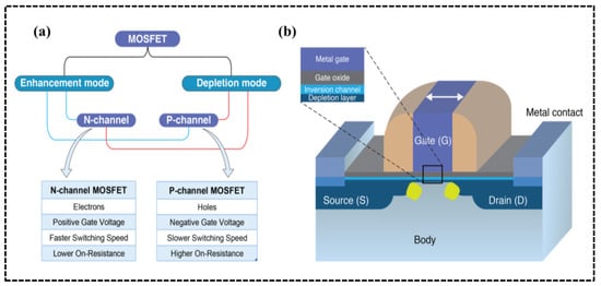
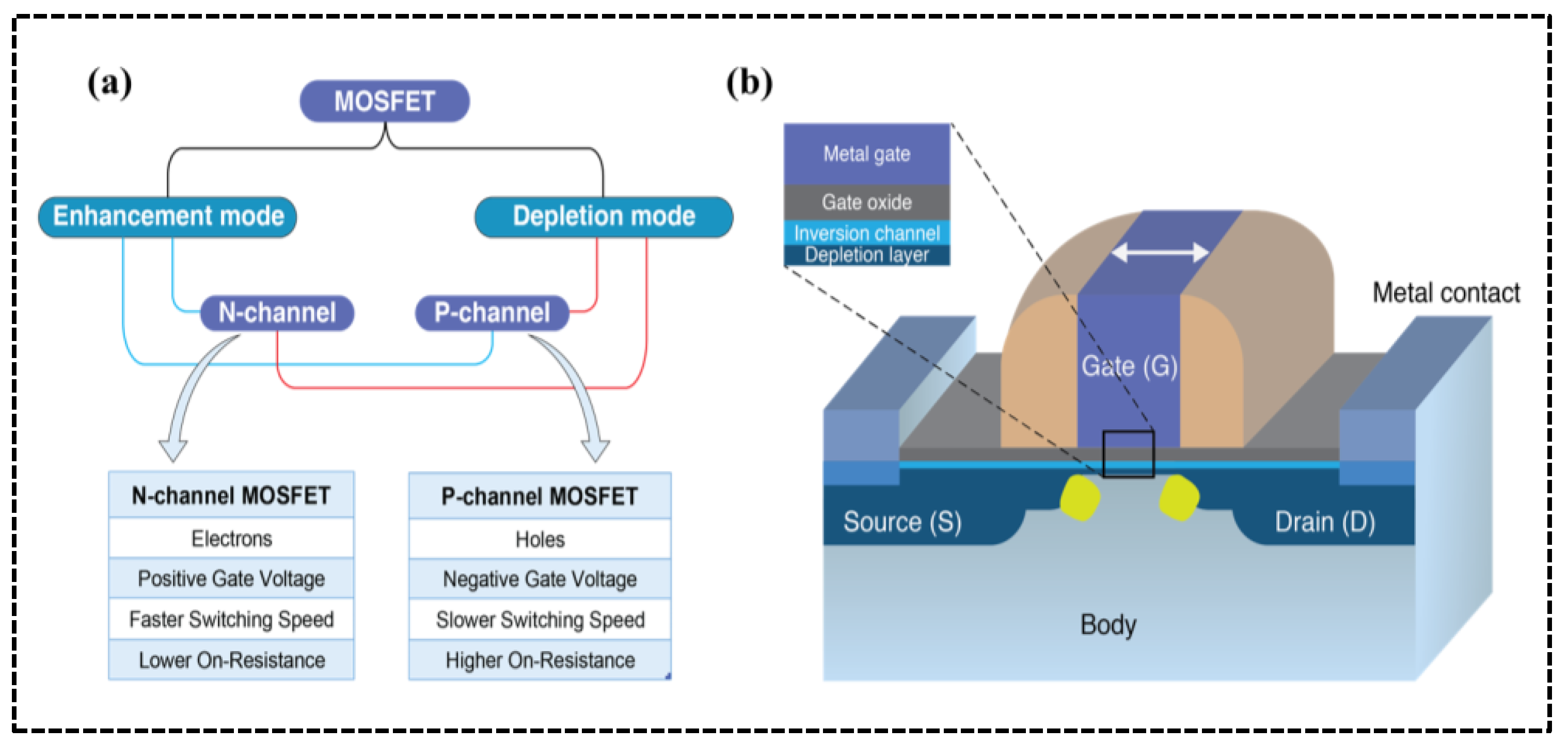
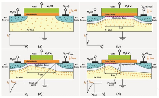
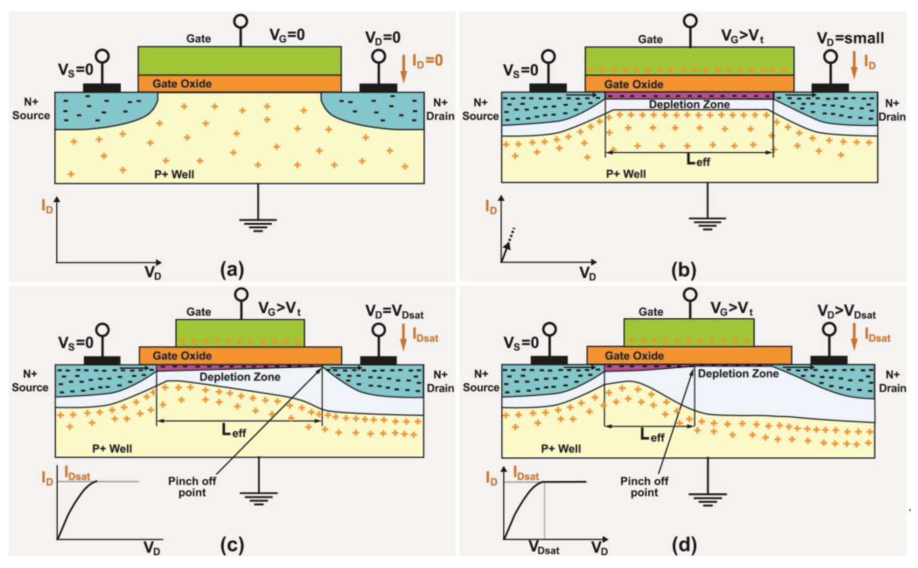
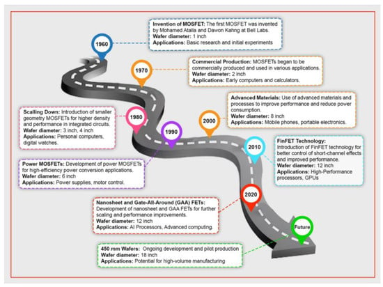
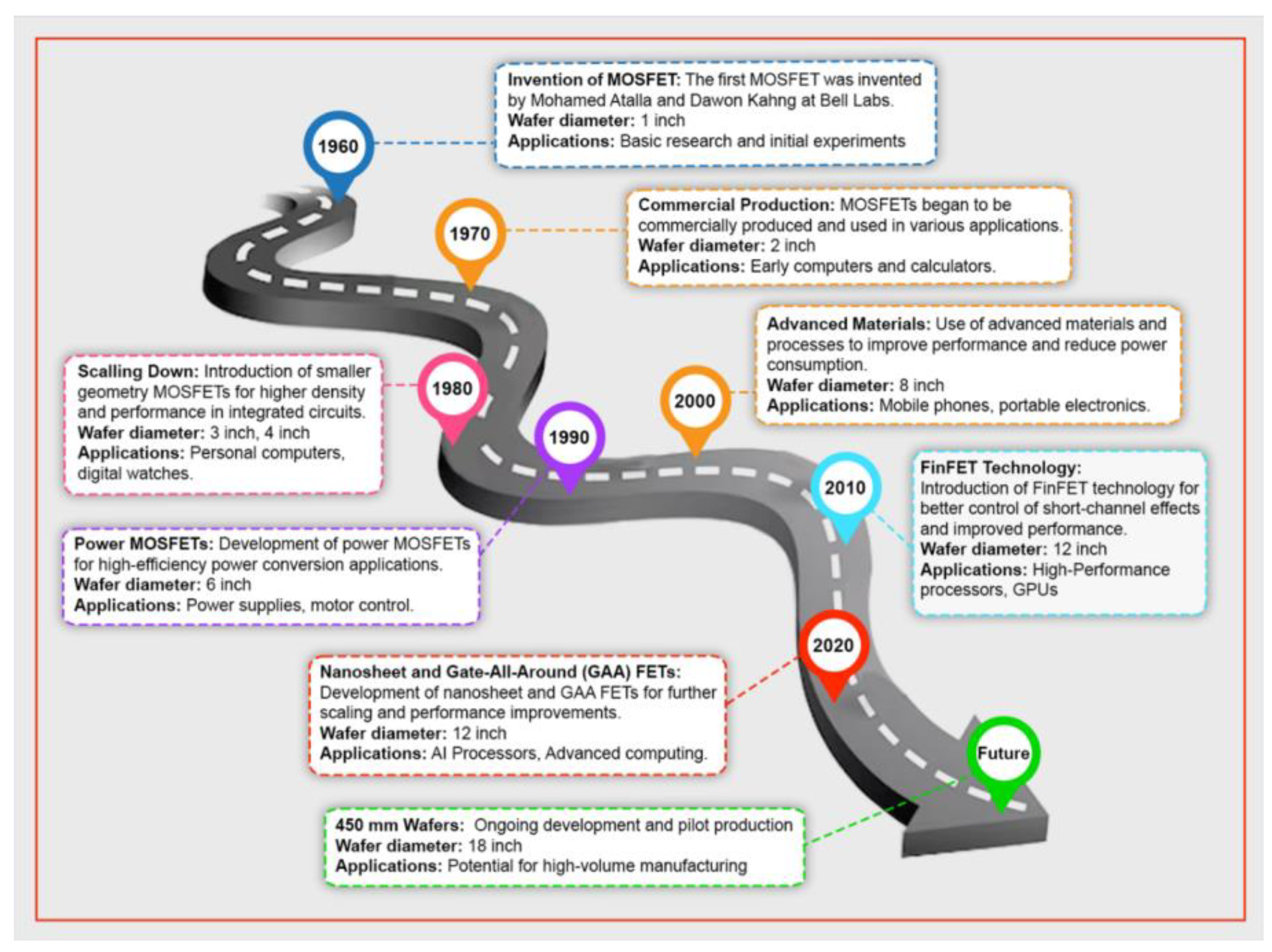
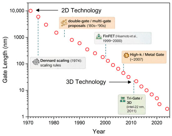
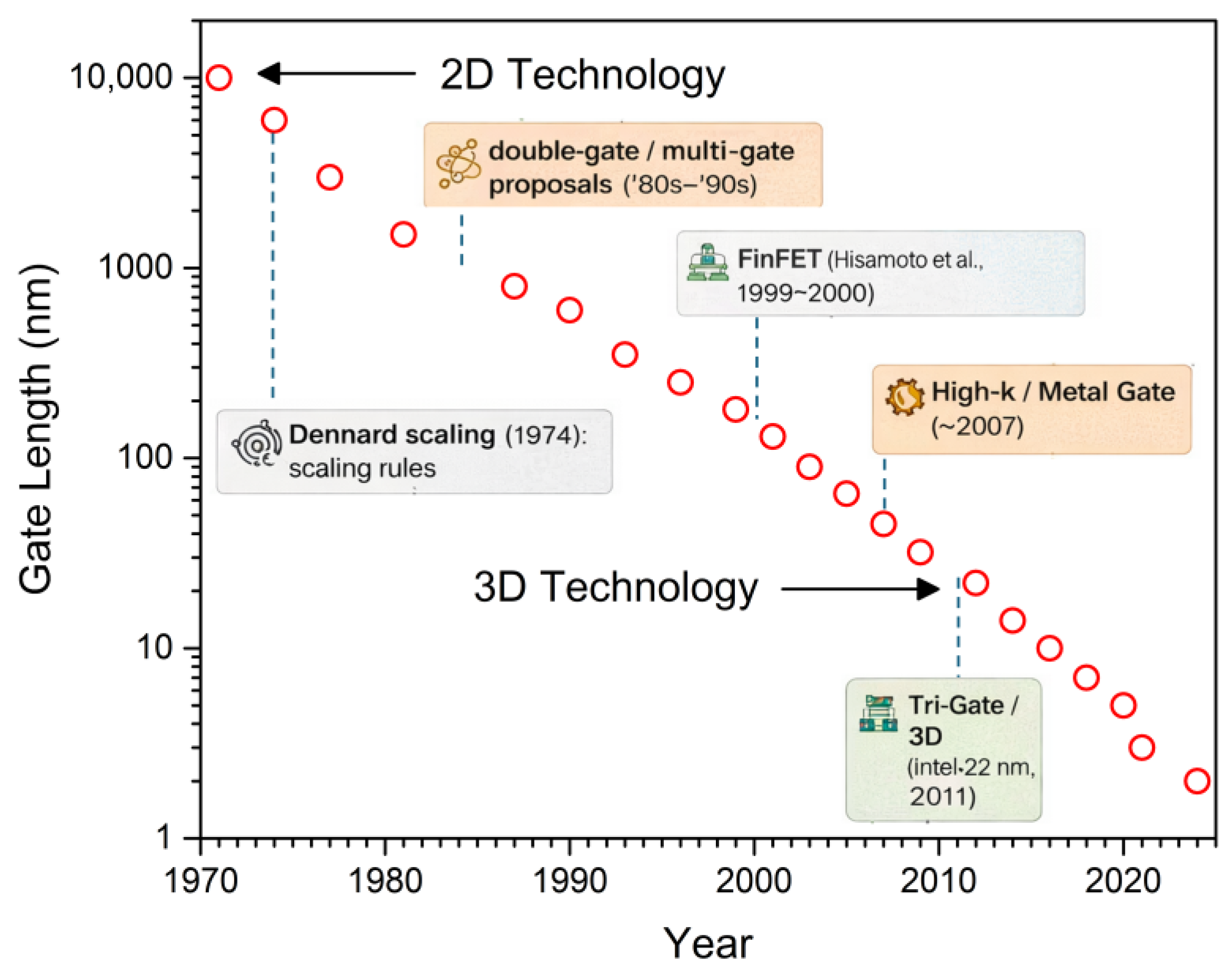
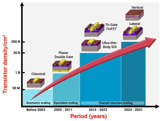
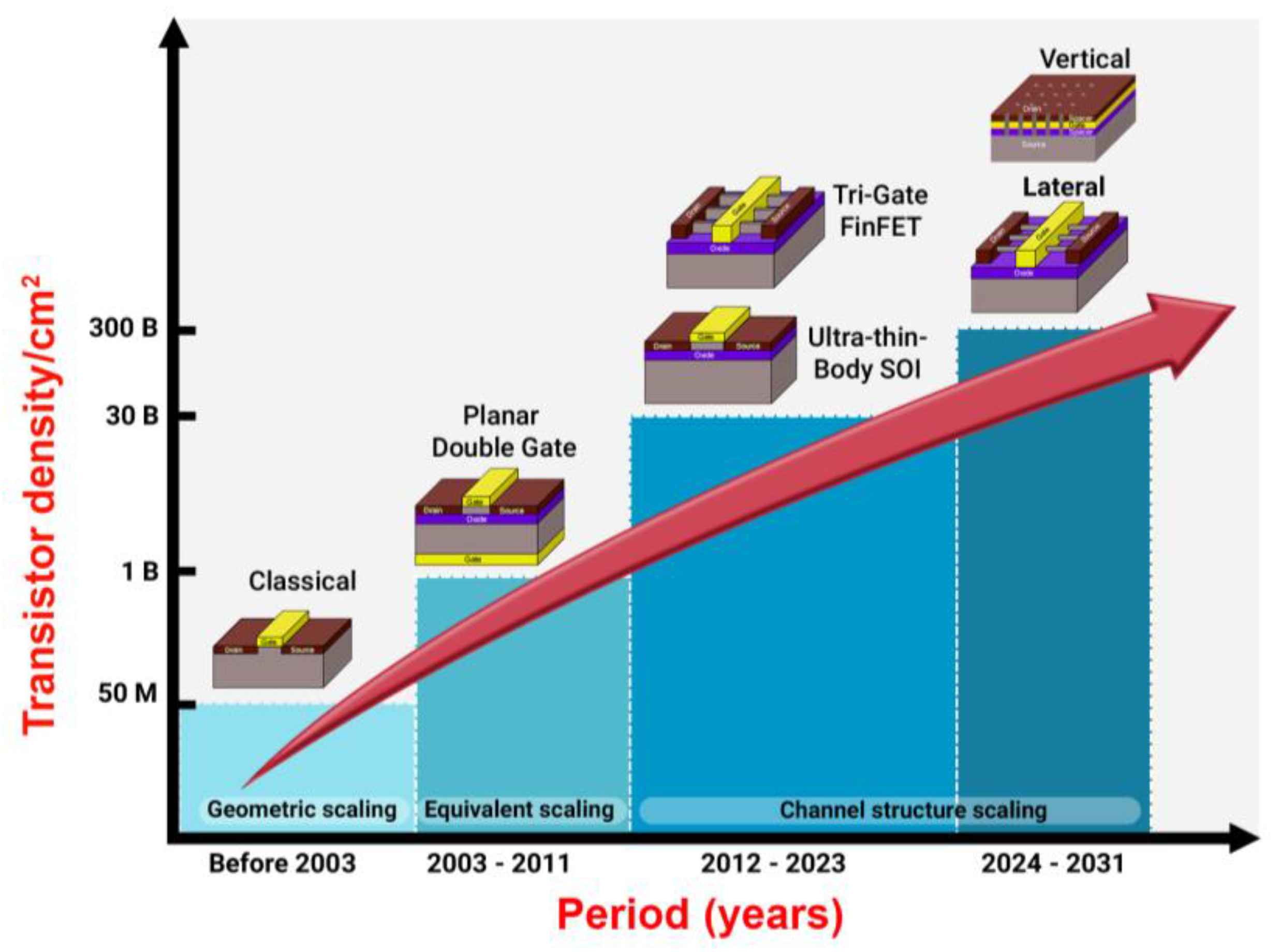
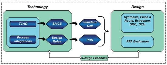
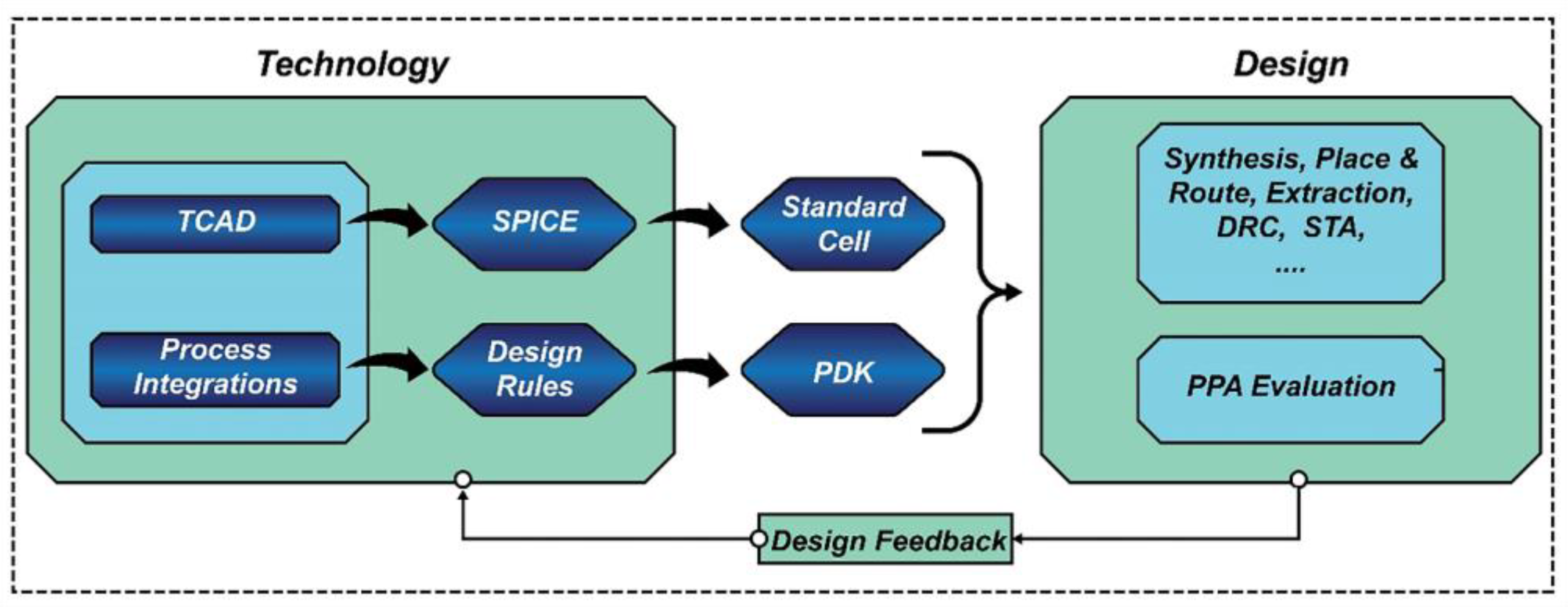
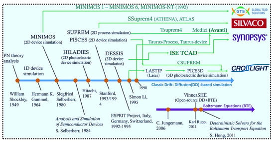
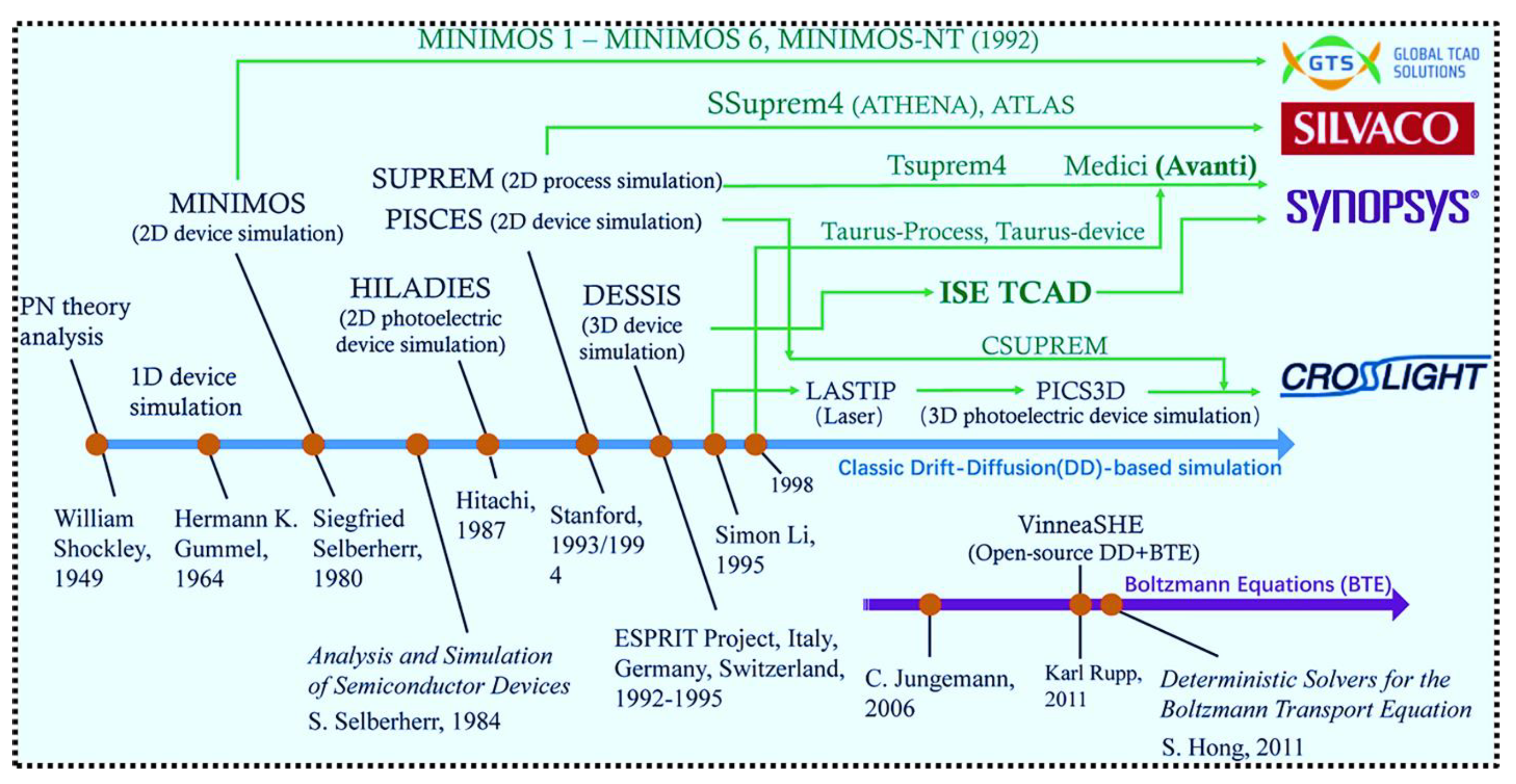
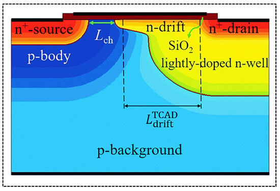
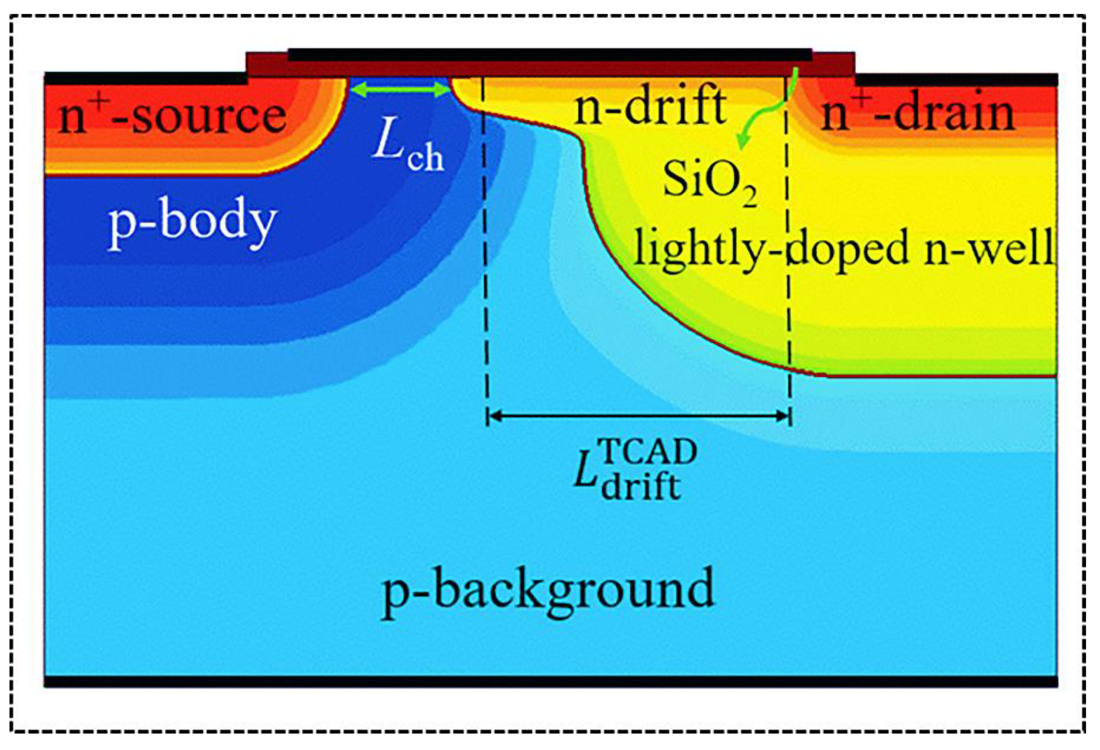
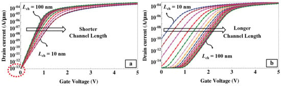
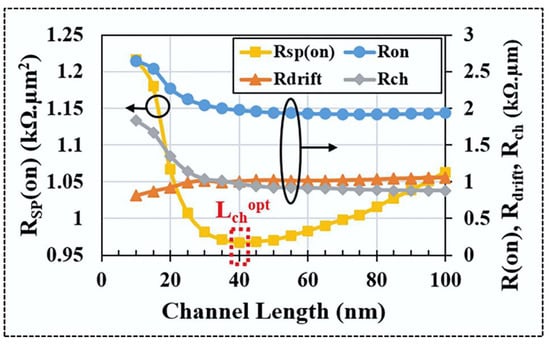
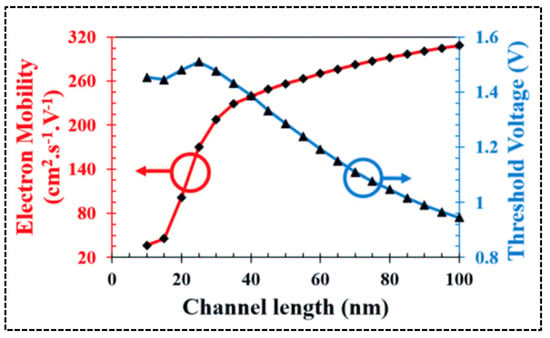
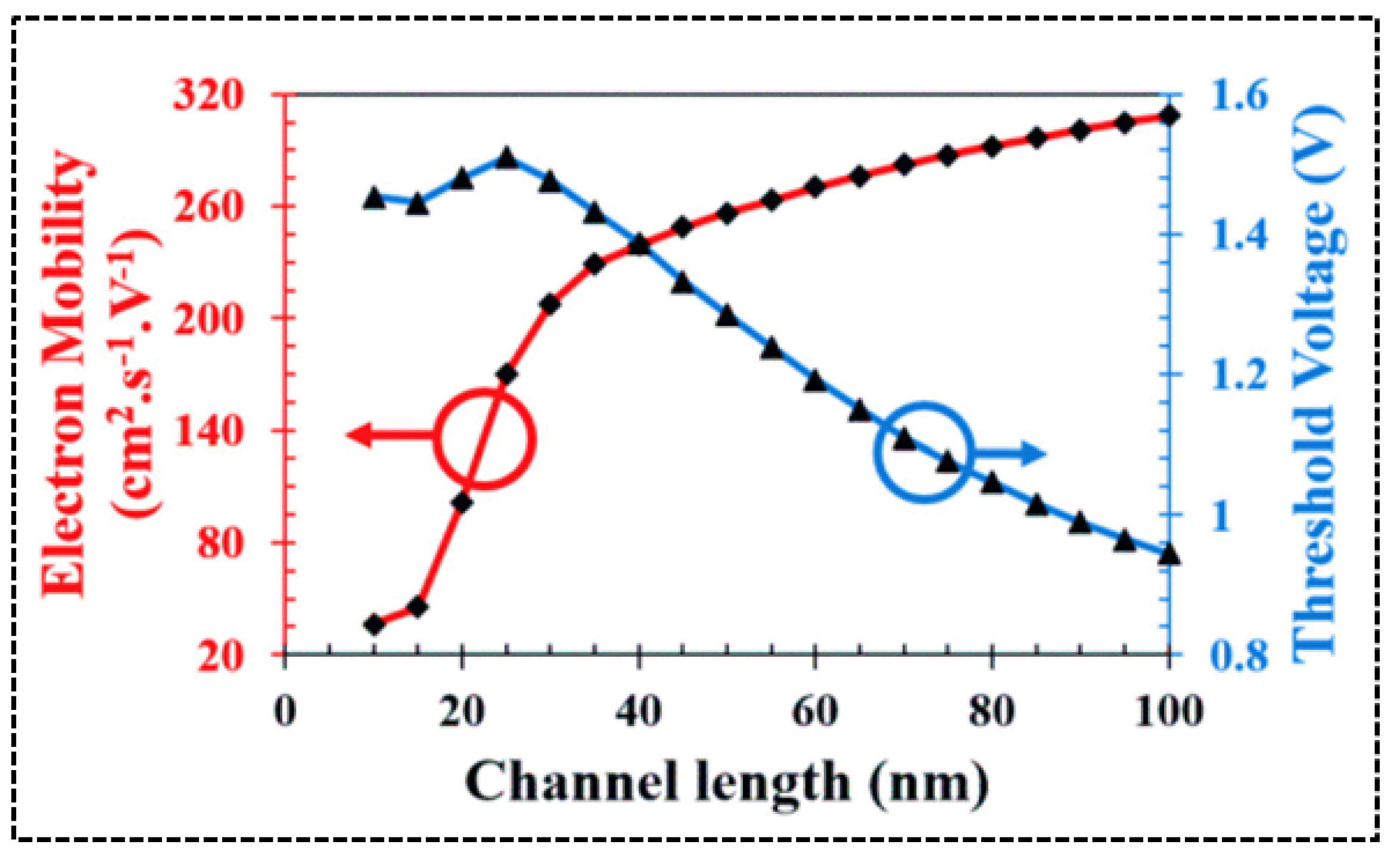
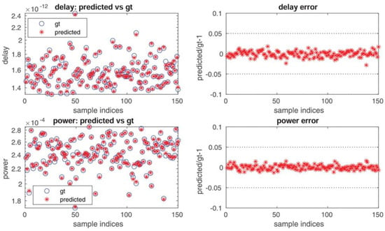
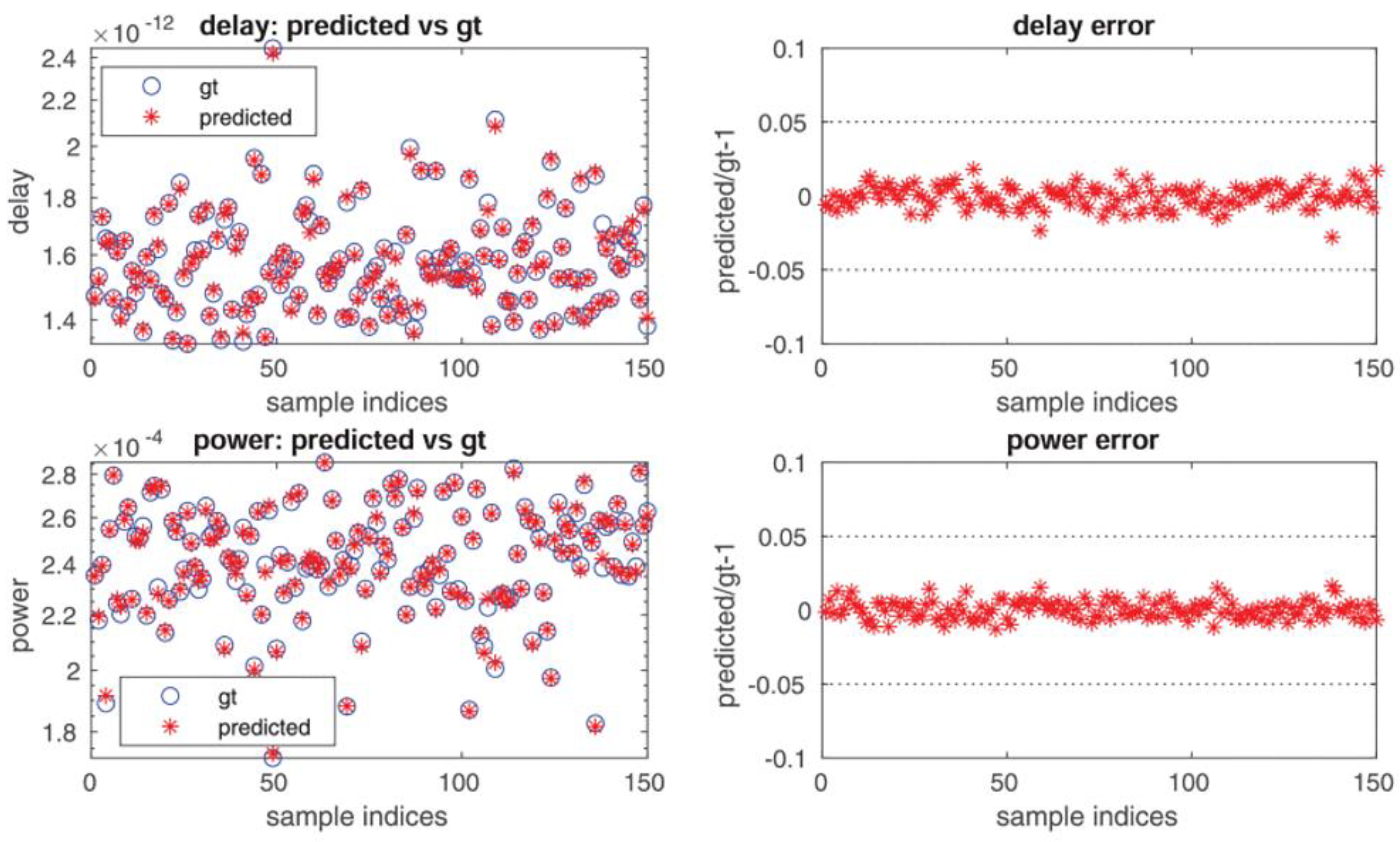
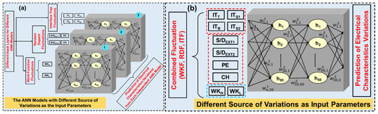
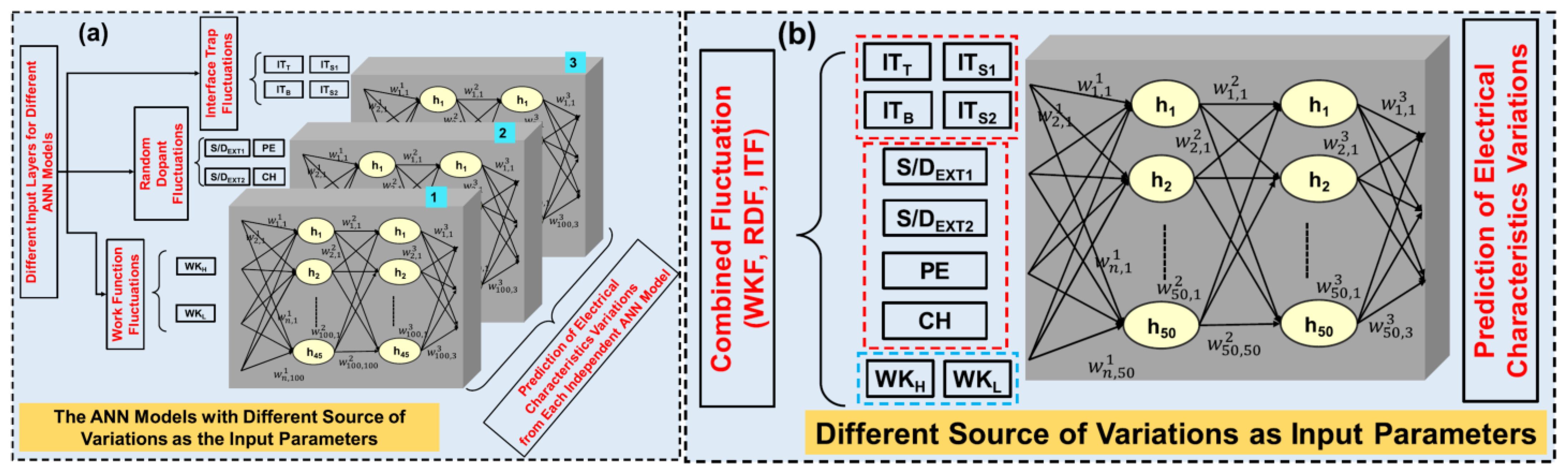
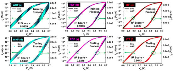
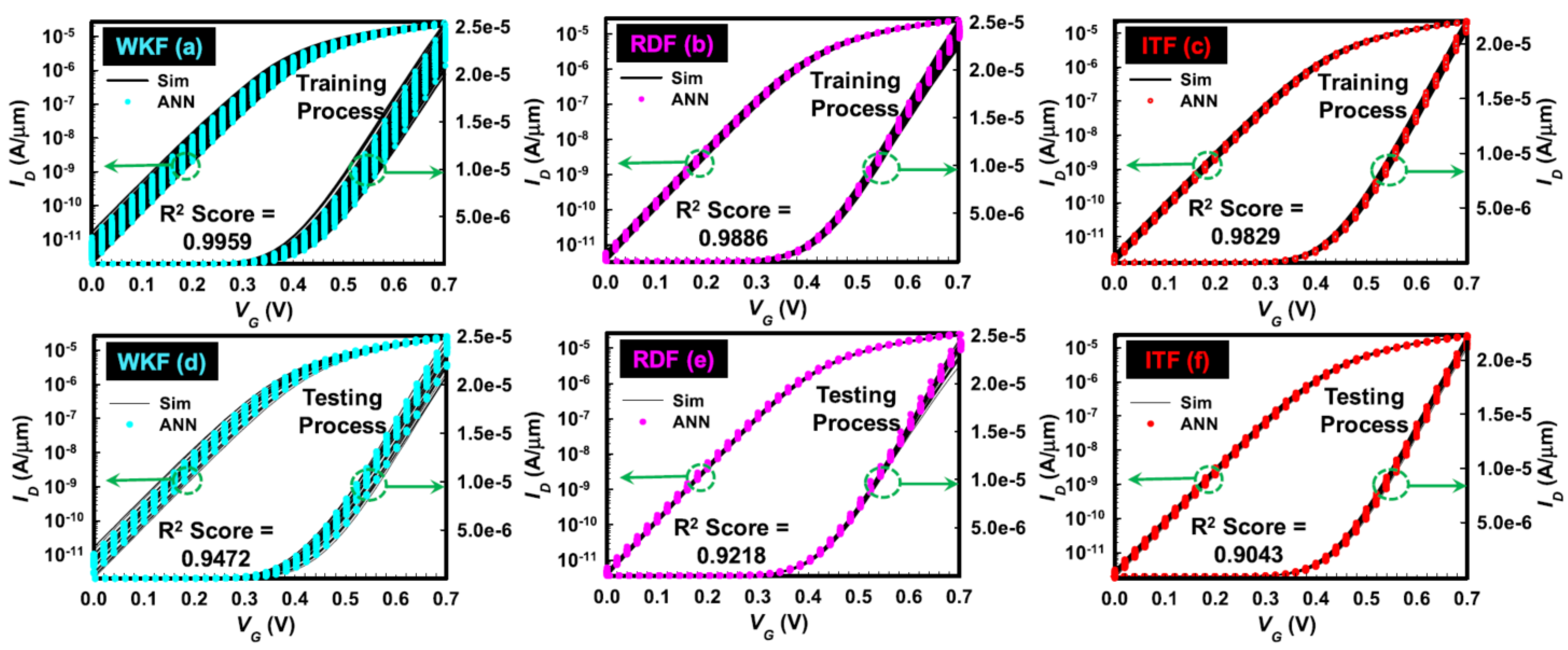
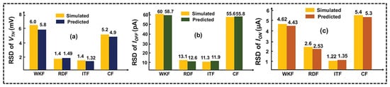
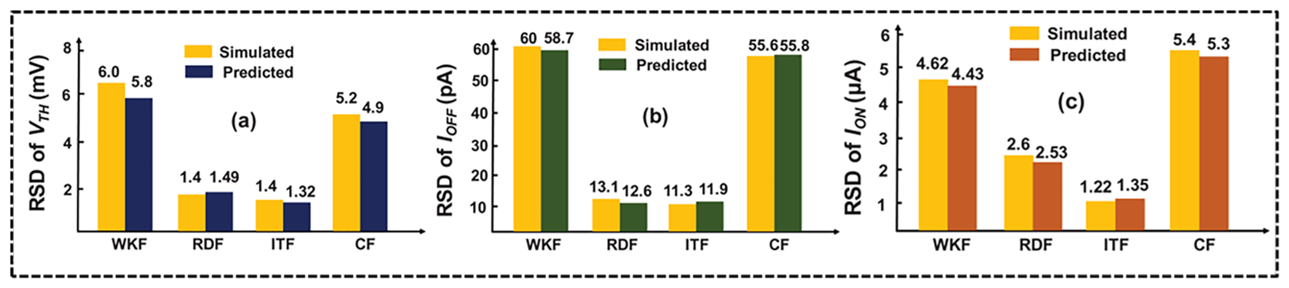
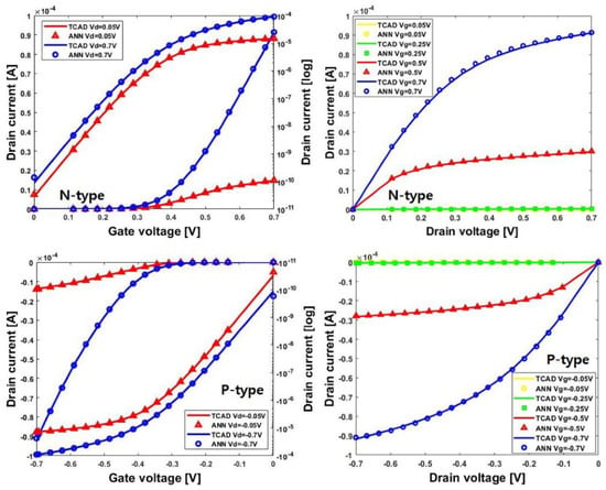
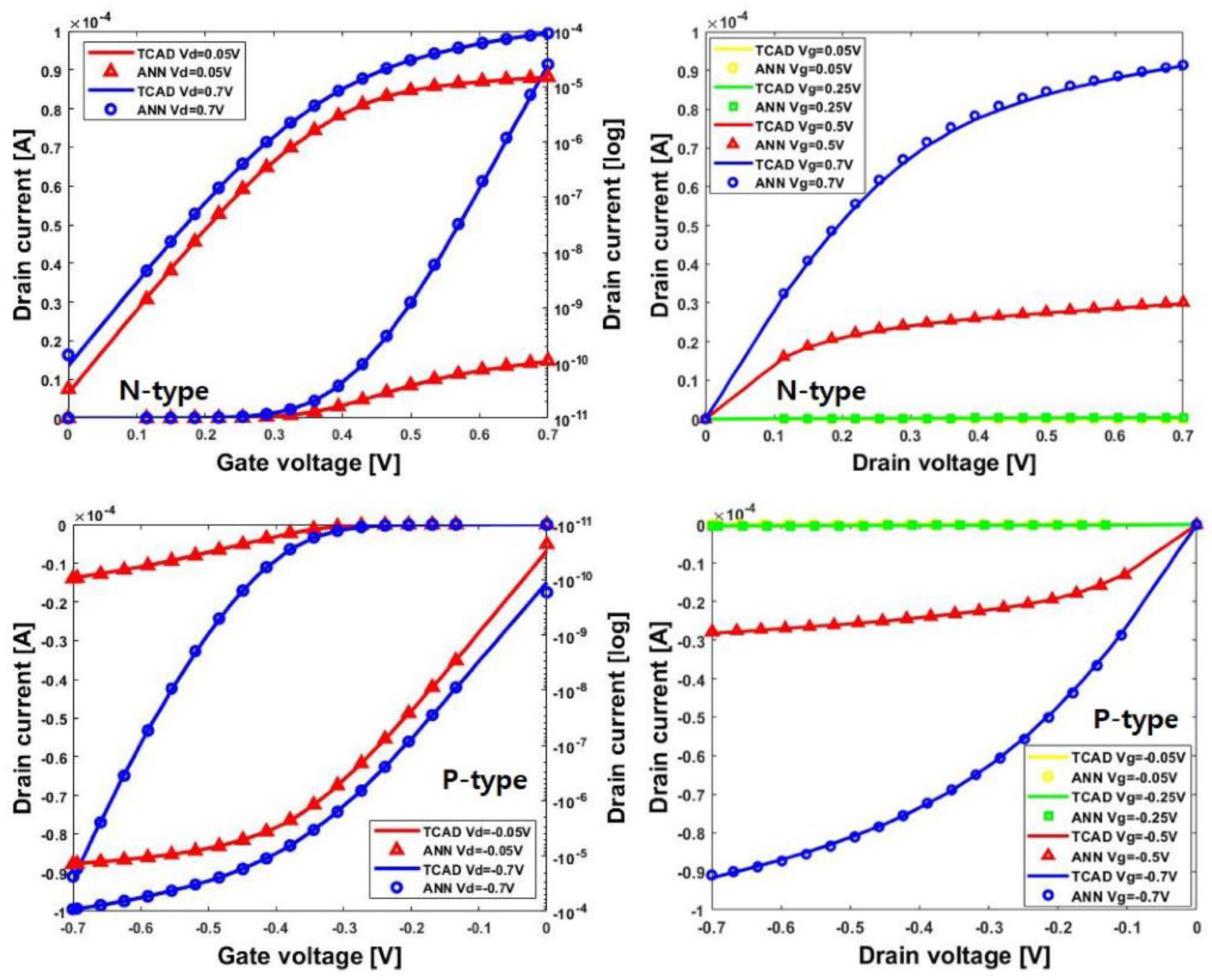
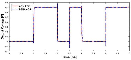
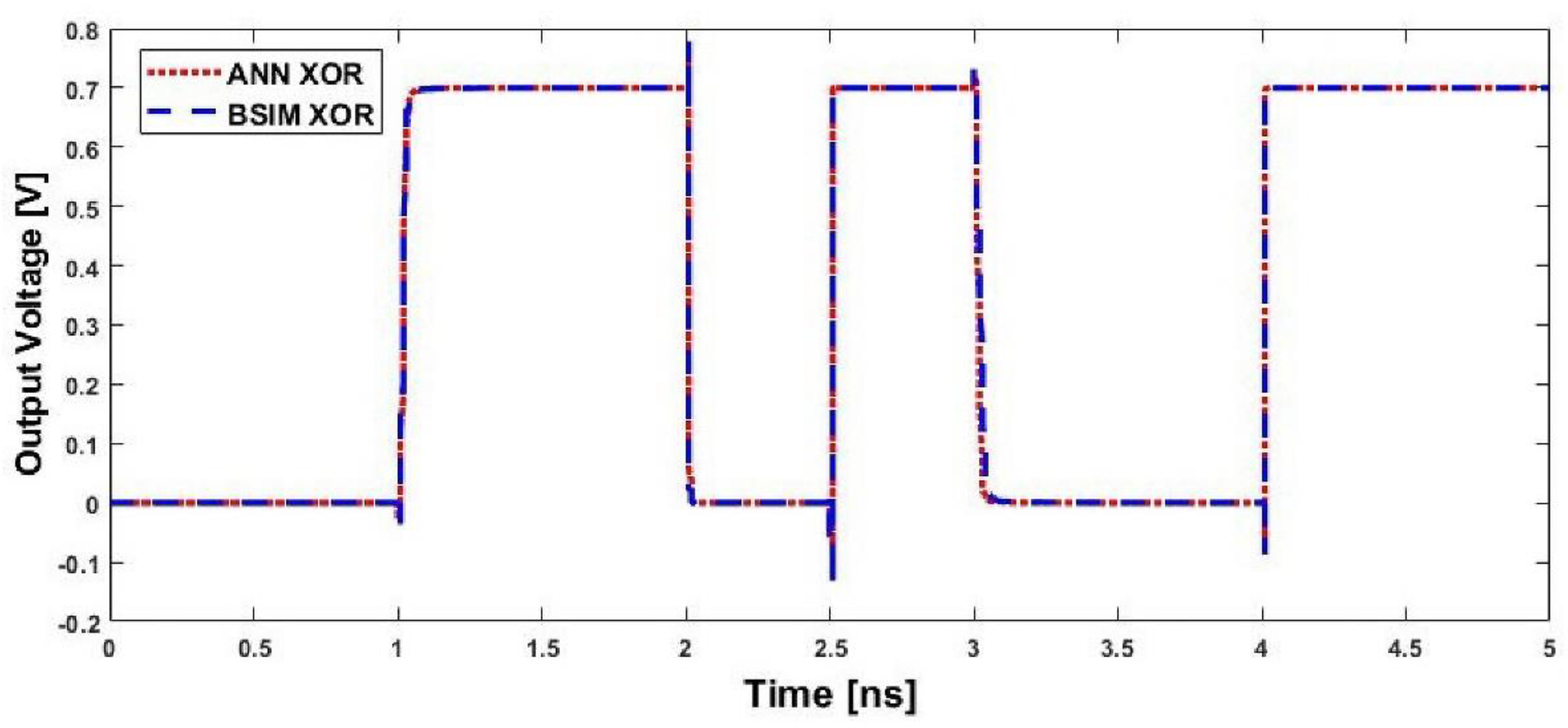
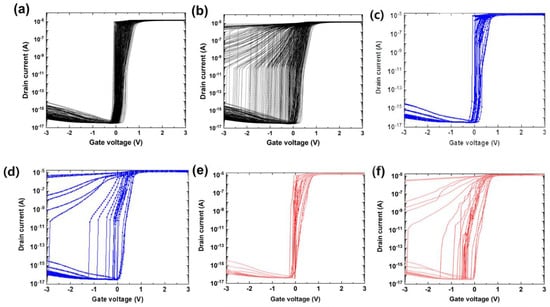
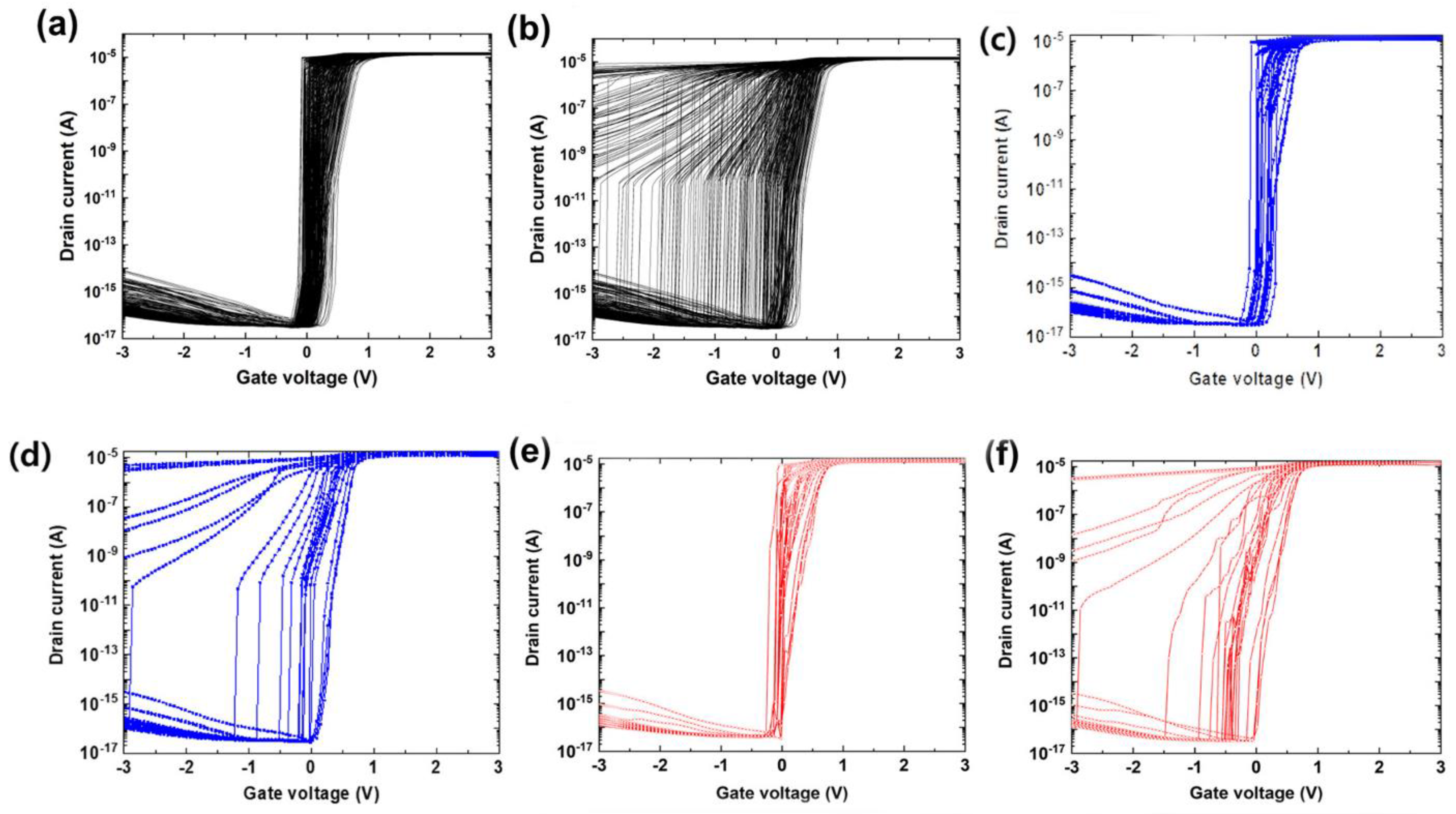
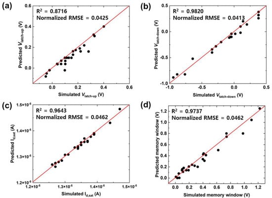
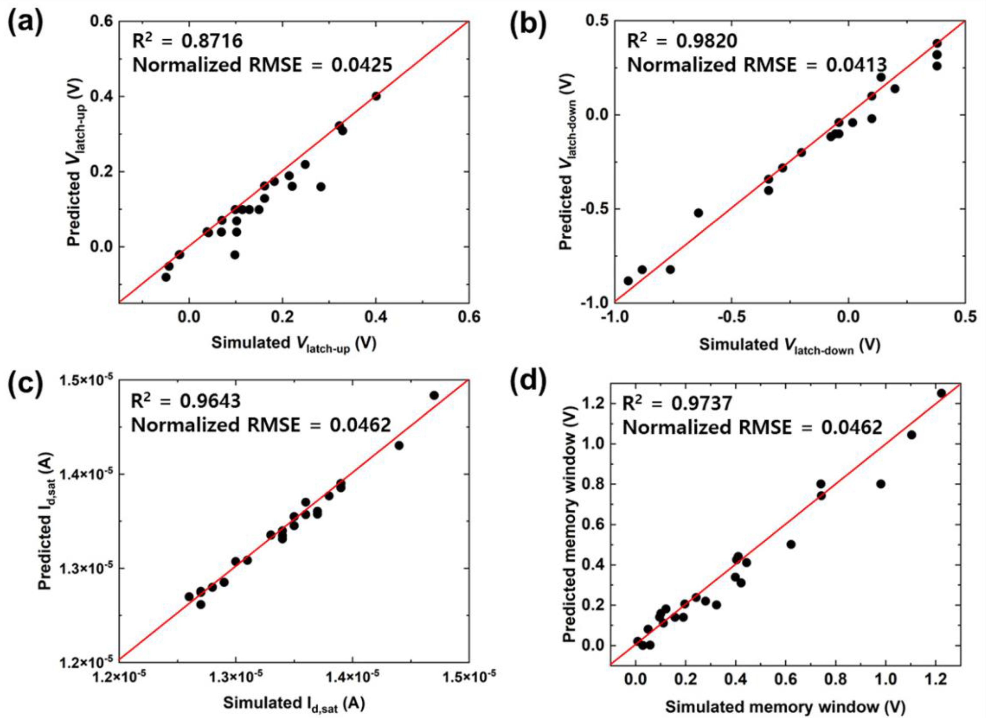

Disclaimer/Publisher’s Note: The statements, opinions and data contained in all publications are solely those of the individual author(s) and contributor(s) and not of MDPI and/or the editor(s). MDPI and/or the editor(s) disclaim responsibility for any injury to people or property resulting from any ideas, methods, instructions or products referred to in the content. |
© 2025 by the authors. Licensee MDPI, Basel, Switzerland. This article is an open access article distributed under the terms and conditions of the Creative Commons Attribution (CC BY) license.