1. Introduction
Modern technology continues to evolve through extensive research aimed at making nearly all sectors smarter and integrating them with artificial intelligence. At the core of this infrastructure lie data collection, transmission, and processing. Data communication, which is realized by transferring data from one point to another, has become one of the fundamental elements of today’s information and communication technology industries. In today’s world, the vast majority of devices support data communication. Computers, mobile phones, and industrial devices, which have become indispensable devices in our daily lives, transmit data over wired or wireless media, enabling information sharing in a fast and effective way [
1].
Data communication can be carried out in two ways: analog or digital. The increase in data size has made the speed and spectral efficiency of communication technologies highly significant. Three fundamental techniques—modulation, coding, and multiplexing—have continuously evolved in response to past and present technological needs and are now employed across all communication infrastructures.
Modulation, coding, and multiplexing are essential electronic techniques used to efficiently transmit information from one location to another. Modulation adapts the information signal to the transmission medium, enabling more efficient and reliable transmission, while multiplexing allows multiple signals to be transmitted simultaneously over a single transmission channel. Coding enhances communication efficiency by converting digital data into digital signals. These techniques are indispensable for the optimal functioning of communication systems and serve as the fundamental building blocks of electronic communication [
2]. They can be applied in both analog and digital data transmission.
There are two methods of digital data transmission: serial and parallel. Serial data transmission is preferred over parallel communication because it is more reliable over long distances, easier to implement at high speeds, and more cost-effective. Many protocols, such as CAN, I2C, SPI, and UART, use serial data transmission.
In serial data transmission, both binary and multi-level signaling techniques are employed. Multi-level signaling techniques allow saving channel bandwidth without sacrificing bit rate or increasing bit rate without demanding more transmission bandwidth. These techniques significantly enhance the performance of communication systems by improving data transmission efficiency [
3].
In this paper, a new multi-level line coding technique called the “multiplier technique” is proposed [
4]. This technique aims to provide an easy-to-implement and efficient alternative approach to data transmission.
2. Conventional Approach to Serial Data Transmission
Today, many high-speed digital transmission systems, both wireless and wired, rely on multi-level transmission techniques. This is primarily because these techniques enable higher data transmission rates by increasing spectral efficiency (SE, b/s/Hz), which is one of the most critical transmission parameters. Consequently, these techniques facilitate more efficient data transmission within limited bandwidths and enhance the overall performance of communication systems [
3].
M-ary Pulse Amplitude Modulation (M-PAM), M-ary Phase Shift Keying (M-PSK), and M-ary Quadrature Amplitude Modulation (M-QAM) are well-known and widely used modulation techniques in digital data transmission [
5]. M-ary Phase Shift Keying and M-ary Quadrature Amplitude Modulation are also used to implement secure data transmission with quantum communication protocol [
6]. In these modulation techniques, the signal’s amplitude, phase angle, or both are used to transmit data in symbols. M-PAM transmits data by changing the amplitude for each symbol, while M-PSK transmits data using phase shifts for each symbol. M-QAM combines both amplitude and phase shifts to achieve higher data transmission rates. These techniques play a crucial role in enhancing the efficiency of modern communication systems and optimizing bandwidth utilization. Although these modulation techniques are classified as digital communication methods, the data they carry is digital, while the modulated signal itself is analog. Line coding techniques are also widely used to improve throughput and communication speed.
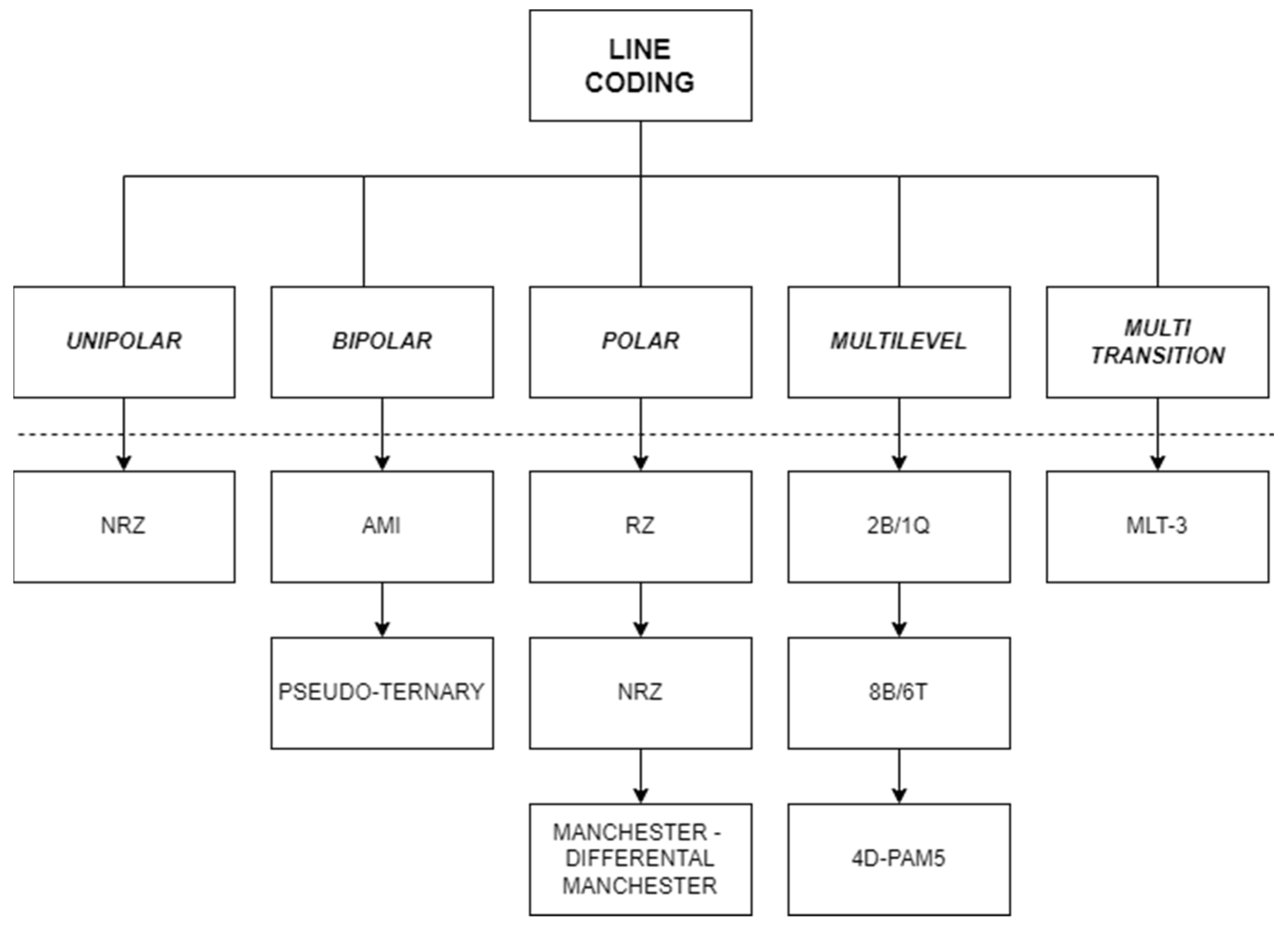
Line coding is a technique used to convert digital data into a digital signal. Various line coding methods exist, and the most commonly used ones are schematically illustrated in
Figure 1 [
7]. Engineers at AT&T, IBM, or RCA mostly created line codes in the 1960s for digital recording on magnetic media or digital transmission over telephone wires [
8,
9,
10,
11]. Subsequently, fiber optic communication methods and wireless methods became a major focus of line code advancements [
12,
13,
14,
15,
16,
17,
18,
19].
The most commonly used line coding methods are shown in
Figure 2 [
20]. These techniques are employed in various communication infrastructures, including DSL, Ethernet, and fiber optics.
The multiplier technique proposed in this paper is a new multi-level line coding method. An example coding signal is shown in Figure 5.
3. Proposed Approach: Multiplier Technique
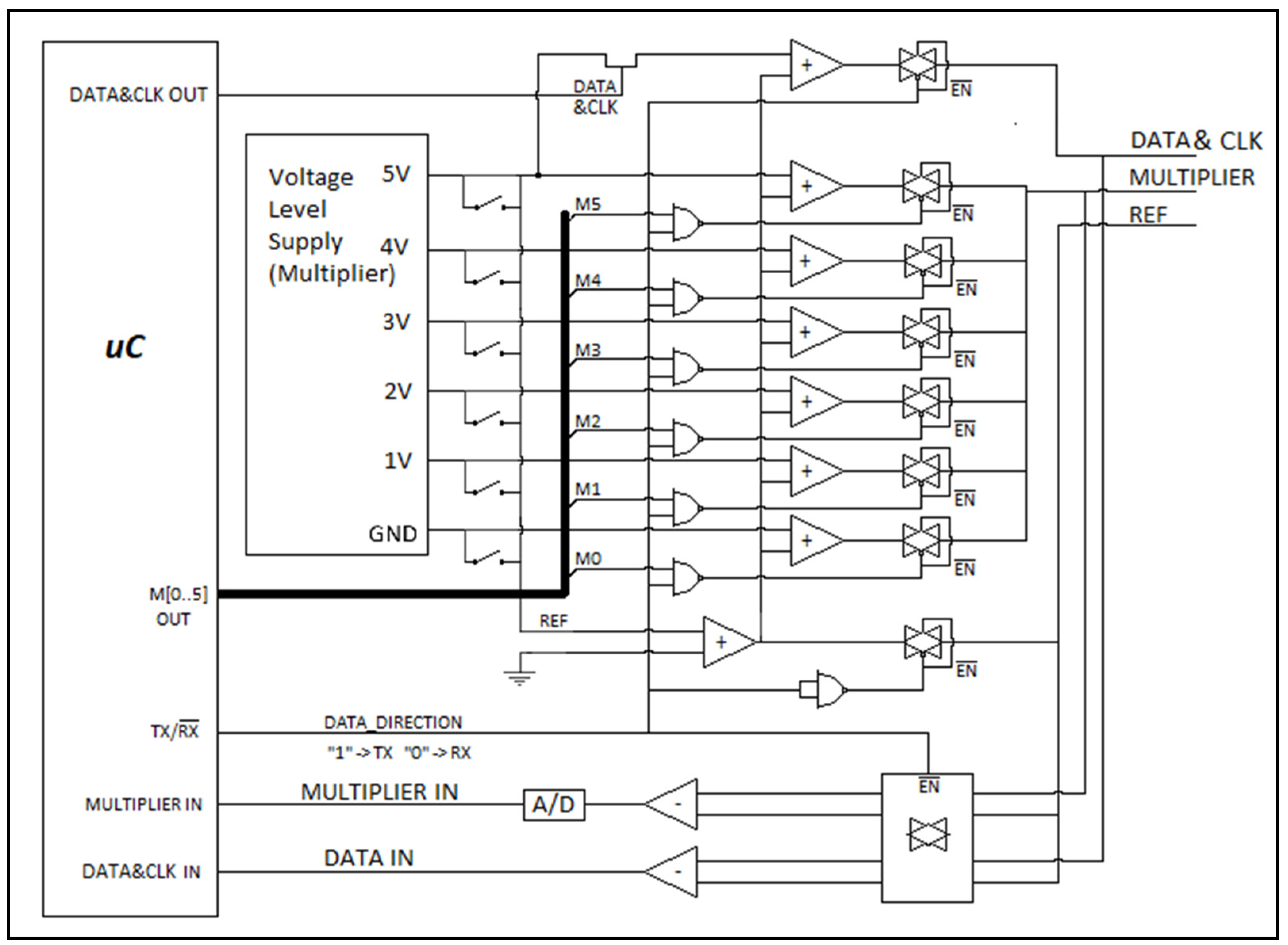
The block diagram of the multiplier technique is shown in
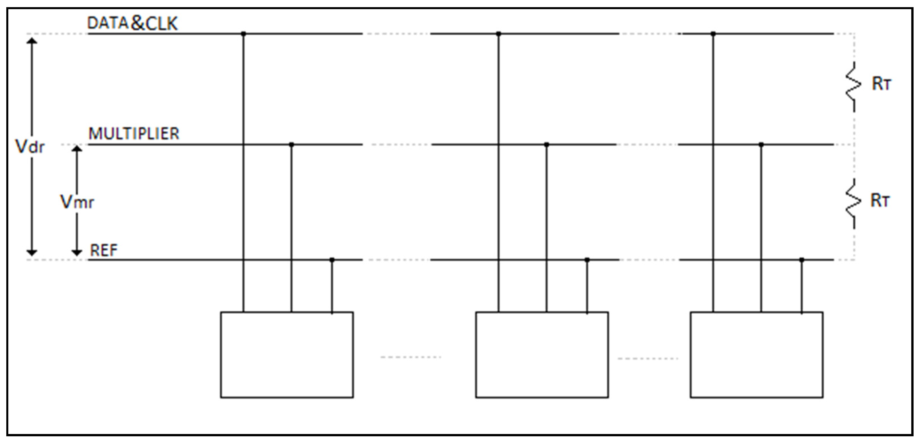
Figure 3. In this technique, data transmission is based on the deduplication of repeated data. At the sender side, the deduplication unit counts the repeated data in the incoming data, generates multiplier values of data, and transmits them to the receiver via the line. The deduplicated data count is transmitted to the receiver as a multiplier, enhancing the efficiency of the transmission process. During data transmission, operations are performed on the rising and falling edges of the DATA/CLK signal. On the receiver side, the data replication process is triggered by this signal to ensure synchronization. To perform these operations, at least three lines are required in wired communication: a Data (DATA/CLK) line, a Multiplier (MULTIPLIER) line, and a Reference (REF) line.
The network topology for single-multiplier communication is shown in
Figure 4. Due to data deduplication, changes in the data line occur only when there is a logic level transition. This feature allows the data line to function as a clock signal on the receiver side, enabling synchronous communication. The multiplier value is obtained using an analog-to-digital converter (ADC) during data exchanges, ensuring that the required multiplier values are accurately calculated and transmitted throughout the data transmission process.
The multiplier value obtained through the A/D converter and the sample data derived based on the direction of the data & CLK signal are presented in
Table 1.
Since this study was carried out on a short distance transmission line, the noise impact is minimal. On long distance lines, the noise level can degrade signal integrity. Signal selectivity can be improved by changing the voltage ranges and reference value given in
Table 1.
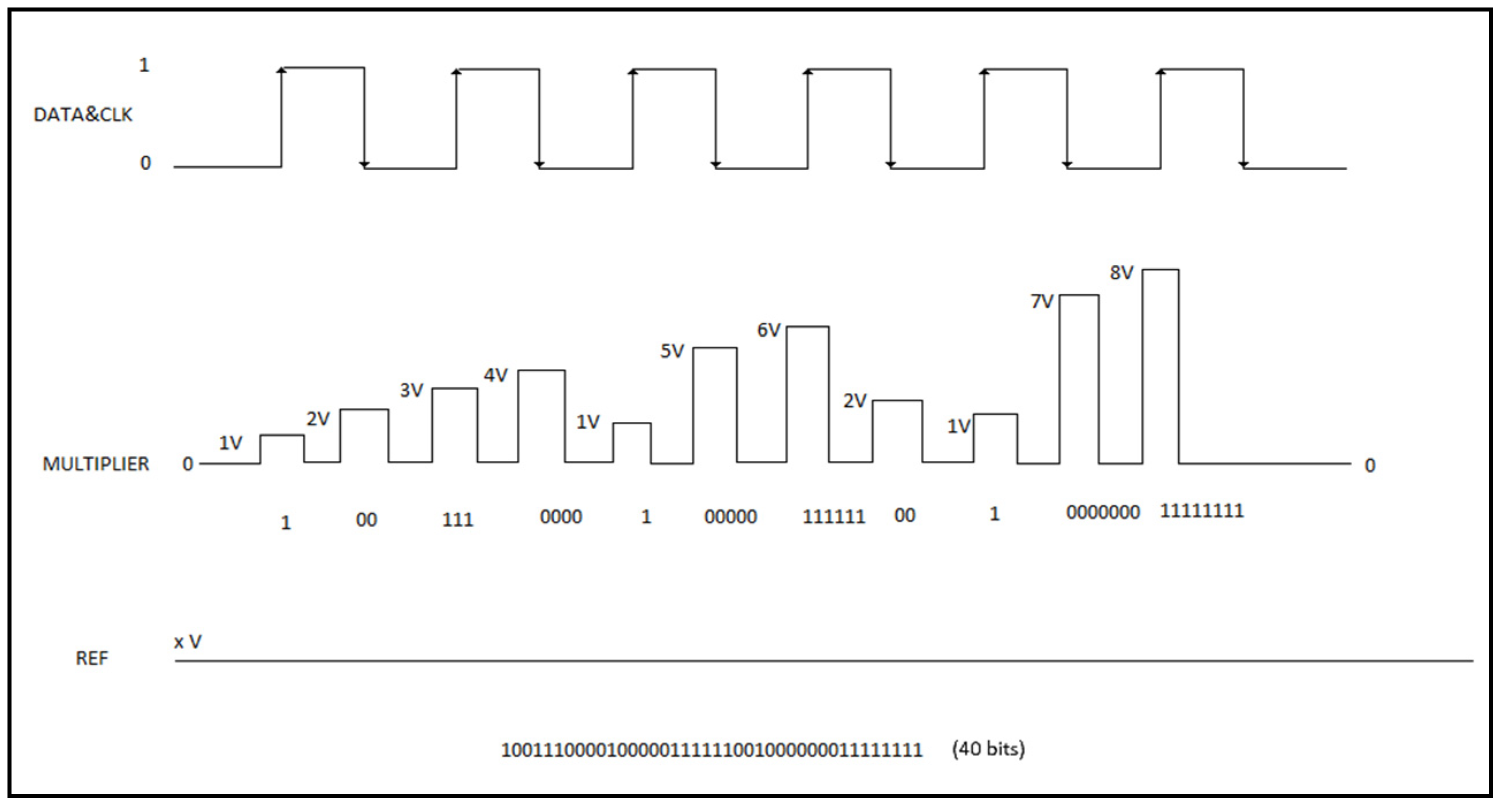
Figure 5 illustrates the signaling process during the transmission of 40 bits of data. In this communication, the DATA/CLK signal represents logic ‘1’ on the rising edge and logic ‘0’ on the falling edge. The transmitter conveys data by adjusting the position of the DATA/CLK signal and determining the number of repetitions of the logic value as the level (amplitude) of the multiplier signal. In
Figure 5, 40 bits of data are transmitted using six clock cycles.
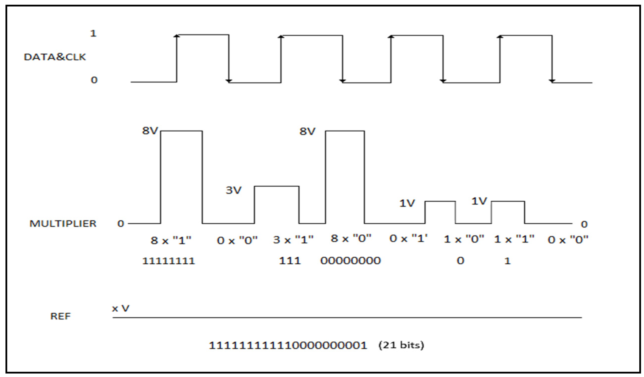
Considering the potential issue of an insufficient multiplier value, i.e., when the number of repeated data exceeds the maximum multiplier value, this problem can be resolved as shown in
Figure 6. When the multiplier value is zero (equal to the reference), it is corrected by switching the DATA & CLK signal. For example, in
Figure 6, the maximum multiplier value is set to 8. To send 11 logic ‘1’ values, a zero multiplier is used in between to ensure data transmission.
To minimize multiplier insufficiency, the multiplier level can be increased, or a multi-multiplier network topology can be implemented, as shown in
Figure 7. In this topology, the multiplier value can be raised to higher levels by increasing the number of multiplier components. For example, a multi-level multiplier structure defined as Multiplier = Multiplier-1 × Multiplier-2 helps overcome inefficiencies encountered during data transmission by increasing the multiplier value.
4. Application
In the application part of the study, an interface for data transmission using the multiplier technique was designed, and a basic protocol was developed. This interface ensures that the data flow is synchronized by effectively utilizing the multiplier technique during data transmission. The protocol increases the reliability of communication by specifying the fundamental rules necessary for the correct transmission and reception of data. This application demonstrates how the multiplier technique works in practice and how data transmission can be achieved efficiently.
For the interface design, a microcontroller, logic gates, and analog switches were used to analyze, deduplicate, and replicate the data. The design was carried out while staying within the logic voltage level range. The microcontroller enables data to be processed and made available for transmission. The logic gates are used for the correct routing and processing of the data signals, while the analog switches are used for the transmission of the data and the multi-level multiplier signal.
4.1. Interface
As shown in
Figure 8, tri-state analog switches were used to allow multiple devices to communicate on the same line. These switches ensure that only one device transmits data during communication. On both the transmitter and receiver sides, the analog switches were set to high-impedance mode, allowing data transmission only by the required devices. NAND gates were used for this purpose. When the bit that determines the data direction (TX/RX) is set to “1”, the transmitting circuit is activated, and the receiving circuit is deactivated. Conversely, When the direction bit is set to “0”, the transmitting circuit becomes passive, and the receiving circuit becomes active. This method ensures efficient utilization of data lines and enables accurate and synchronized communication between devices.
After the deduplication process is completed and the data is prepared for transmission, it is sent to the line through the transmitter.
On the transmitter side, a generator provides the multiplier levels. The multiplier value is selected using M(0..5) connections. At the output of the transmitter and receiver circuits, an adder and a subtractor receiver circuit are present. During data transmission, the amplitude of the signal is summed with the determined reference, and at the receiver side, it is processed after subtracting the reference. The reference line is used for long-distance communication and to reduce the effect of noise. When signals are sent or received, it is used as an offset value by adding or subtracting it from the reference value as shown in
Figure 8. Therefore, three lines were needed. This approach enhances signal selectivity, particularly in cases where the transmission line is long. In this application, the reference value is selected as GND. Therefore, no adder or subtractor circuits are required.
On the receiver side, for each rising and falling edge from the DATA & CLK line, the multiplier value from the MULTIPLIER line is detected by the A/D converter. Through this process, data replication is performed, and the original data is reconstructed. The A/D converter converts the analog multiplier value into a digital format, ensuring accurate reproduction of the transmitted data at the receiver.
In this study, PIC18F25K22 microcontroller, 74HC00N NAND gates, CD4066 analog switches, and internal A/D converter were used as circuit components. The PIC18F25K22 microcontroller was used to perform data processing and control tasks, while the 74HC00N NAND gates were used to execute logic operations. The CD4066 analog switches were preferred to provide high-impedance mode on data lines and to control data routing. Printed circuit boards were designed and produced, and tests were carried out between the two devices by connecting them as shown in
Figure 9.
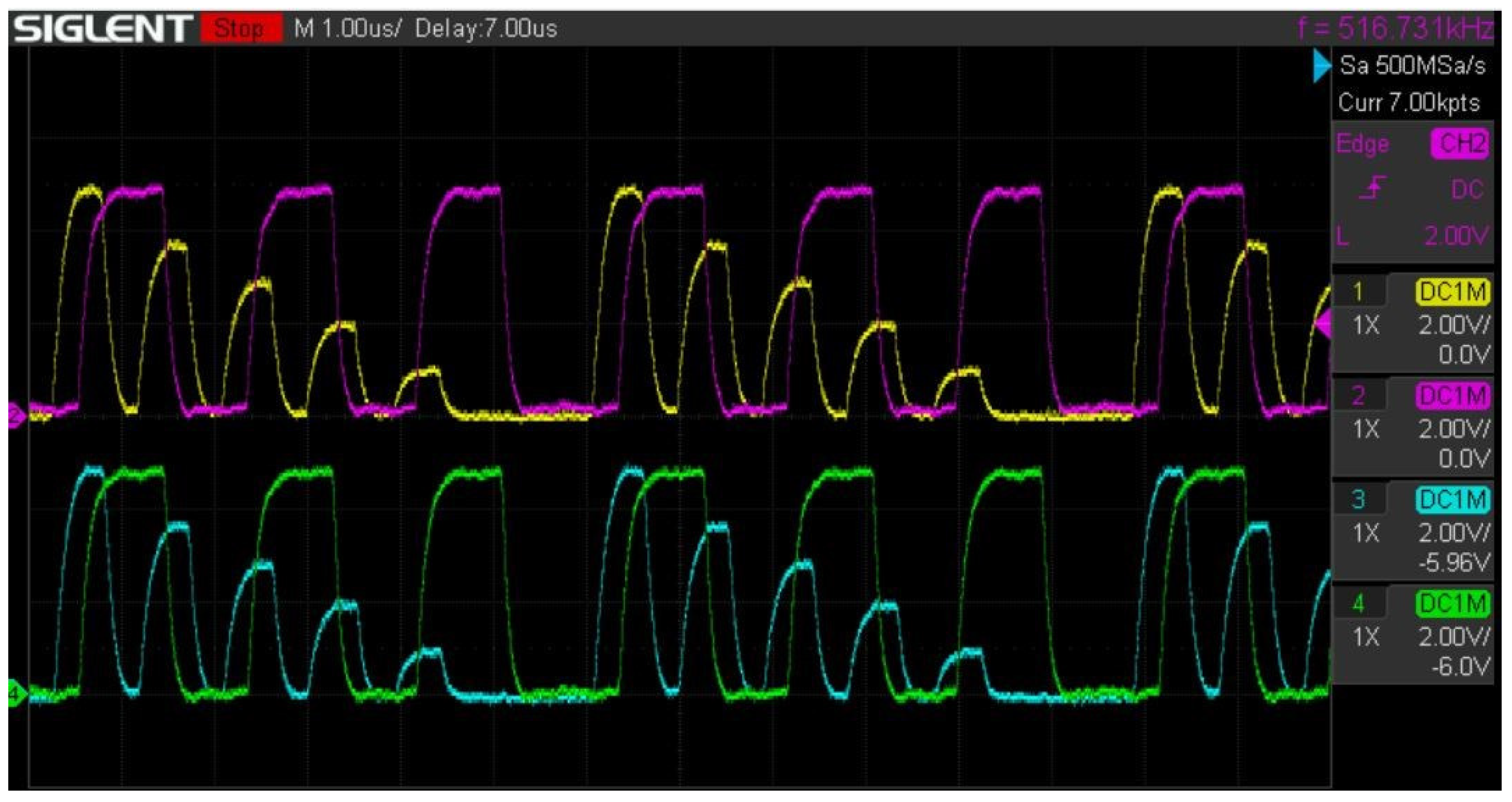
The data sequence “111110000111001” was continuously transmitted to the line, and
Figure 10 clearly shows successful signal transmission. Data transmission at a frequency of 516 kHz was successfully achieved with these components. However, the internal A/D converter could not operate at this speed. One of the critical parameters in designing semiconductors for such systems is the A/D conversion time.
Bitrate (BR) Calculation
The multiplier technique has a dynamic bandwidth (BW). According to the formula proposed by Harry Nyquistin in 1927 [
3],
Assuming that the number of repeated data reaches the maximum multiplier and there is a regular transition of logic levels:
Sample data: “11111000001111100000………”
If there is no repeated data in the transmission, the minimum bit rate is calculated as follows:
Sample data: “10101010101010………….”
4.2. Protocol
A protocol defines the rules, syntax, semantics, synchronization, and possible error recovery methods necessary for the correct transmission of data within a communication system. Protocols can be implemented using hardware, software, or a combination of both. Communication protocols are generally classified into two main types:
Inter-System Protocols: These protocols are used to communicate between two different systems. For example, they are used to transmit data between a computer and a development board. These protocols enable data transfer between remote devices. Examples include Universal Asynchronous Receiver-Transmitter (UART), Universal Synchronous Asynchronous Receiver-Transmitter (USART), and Universal Serial Bus (USB) [
21].
Intra-System Protocols: Inter-system protocols are used to communicate between two devices within the same circuit board or system. These protocols usually fulfill the requirements for low-level communication and short-distance data transmission. Examples include Inter-Integrated Circuit (I2C), Serial Peripheral Interface (SPI), and Controller Area Network (CAN) protocols [
21].
Protocols developed using the multiplier technique can be used both as inter-system and intra-system protocols. Each protocol has its own packet structure. For example,
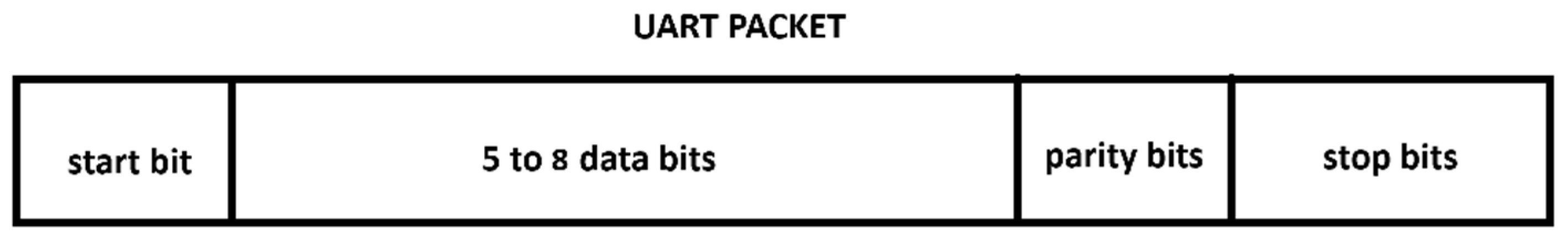
Figure 11 shows the packet structure of the UART protocol.
The basic-level packet structure used is shown in
Figure 12. This packet structure contains the fundamental components required for data transmission. In addition to the start and end bits, the packet content includes essential elements such as the Device ID, which identifies the target device, the Data to be transmitted, and the Block Check Character (BCC) as an error-checking value.
The protocol can be divided into two main parts: data sending and data receiving algorithms.
4.2.1. Data Sending Algorithm
The data sending algorithm consists of three stages.
Preparation of Data Packet: The “Device ID + Data + BCC” information is combined to create the packet to be transmitted.
Preparation of Data to Transmission Line: The generated packet is structured according to the maximum multiplier. For example, if there are eight consecutive logic ‘1’ bits and the maximum multiplier is 5, the packet is organized as 5 × 1, 3 × 1.
Transmission of Data: The data structured for the transmission line is transmitted by adding the start and end bits.
Figure 13 illustrates the flowchart of the data sending algorithm. This flowchart demonstrates how the data sending process occurs, step by step.
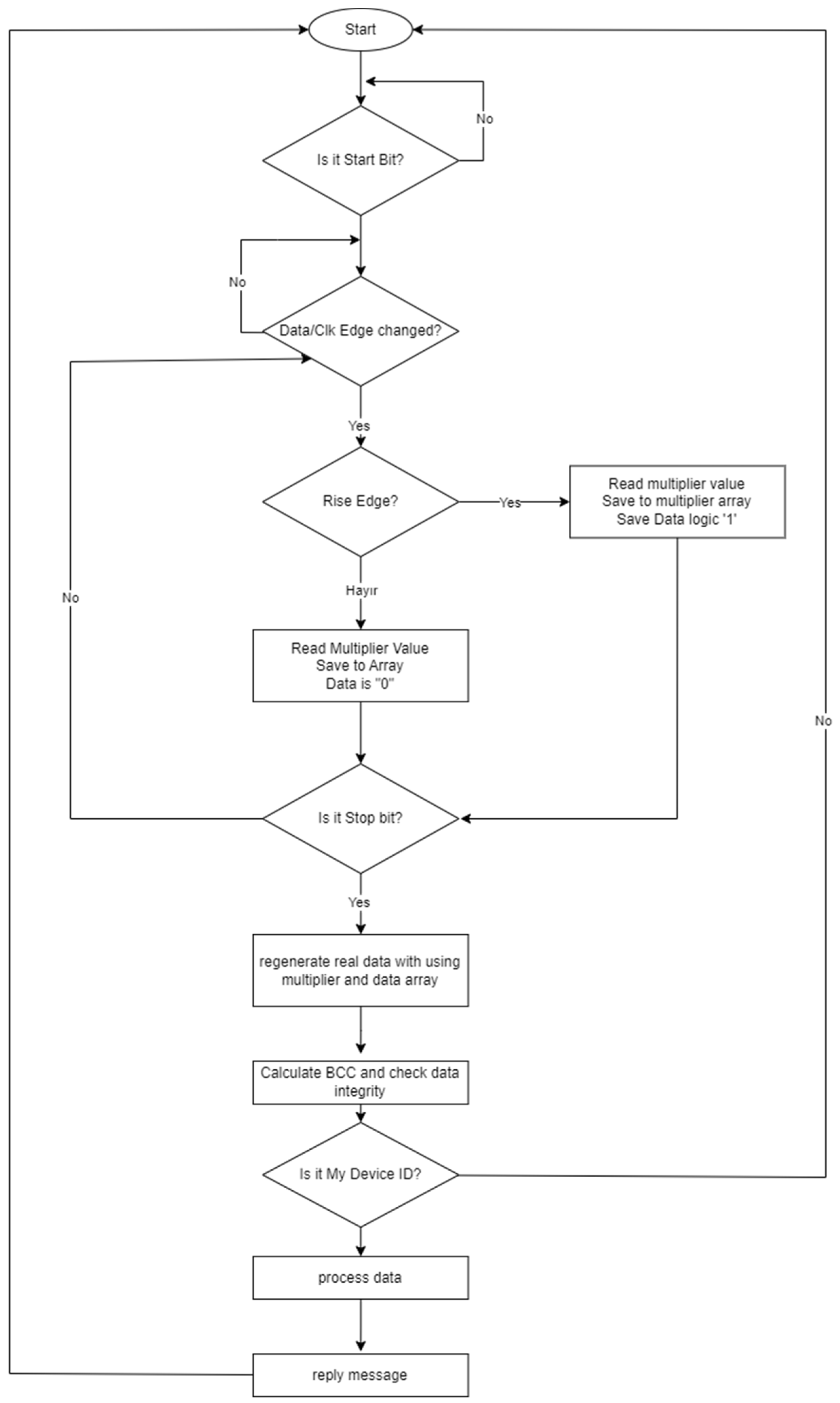
4.2.2. Data Receiving Algorithm
The data receiving algorithm consists of five stages:
Receiving Data: Once the start bit is detected, the data transmission process begins, and the incoming data is stored until the stop bit is detected.
Data Reorganization: The received multiplied values are reconstructed as data of 1-byte length. Example: Data received as 5 × 1, 3 × 1 is reconstructed as ‘11111111’.
Ensuring Data Integrity: The BCC value of the incoming packet is calculated and compared for verification.
Determination of Data Ownership: The Device ID section of the received packet is checked. If there is a match, the data is processed; otherwise, no action is taken.
Reply: A response is sent to the relevant device using the data sending algorithm.
Figure 14 shows the flow diagram of the data receiving algorithm.
With the developed base-level protocol, data communication between devices has been successfully achieved. This protocol defines all the rules, syntax, semantics, and synchronization required for secure, efficient, and error-free data transmission. It also provides protection against possible error conditions and ensures reliable communication.
5. Impact Analysis of Multiplier Value
Theoretically, a system with a multiplier value of “5” can reach a maximum speed that is ten times higher than a system transmitting one bit per cycle. For this to occur, the data would have to continuously follow a pattern such as “0000011111...”. However, the probability of such a scenario occurring in real-world conditions is almost zero. As the amount of repetitive data in the input increases, both speed and efficiency also improve. However, since this varies, the performance of the technique can be evaluated by calculating the average number of cycles.
In this study, the deduplication and replication units were implemented using software. The critical factors here are the buffer size and the multiplier value. When a 32-bit buffer is used, the deduplication process is performed for data of this length, and the multiplier values are generated. To observe the effect of the multiplier value and the bit length of the buffer size, the study used real values instead of pseudocode to generate all data from 8 to 32 bits. Simulations were conducted for multiplier values of 1, 2, 3, 4, 5, 8, 16, and 32, and the average cycle counts were obtained. The summarized results are presented in
Table 2.
It takes approximately 3.6 h to generate results for 232 numbers. However, since calculating all possible variations for 264 with the current system would take approximately 1.7 million years, estimations were made based on the obtained data, and tabular results were derived for larger values.
For each multiplier value, linear, exponential, and polynomial models were developed by analyzing the correlations among the real results obtained for 32-bit data. Error analysis was performed to identify the most suitable model. Linear models were found to be more accurate for longer data ranges, and the
Least Squares Method was used as the regression technique for predictions [
22,
23].
Table 3 presents a few of the models used along with their variance ratios.
The linear models used demonstrate an almost perfect agreement with real data (explained variance ratio R
2 ≈ 0.9999). (Explained variance ratio
R2 ≈
0.9999). The data obtained from these models for high values (2
64) indicate that the cycle gain increases exponentially and converges to 50%, as illustrated in
Figure 15. When analyzed together with
Figure 16, it can be seen that increasing the multiplier and bit length has a positive impact, but the effect saturates at 50%.
In most protocols with an external clock line (I2C, SPI, etc.), one bit of data is transmitted per clock cycle (on the rising or falling edge). As seen in
Table 2, while a 32-bit data is normally sent in 32 cycles, with a multiplier of “5”, it can be transmitted in 16.94901 cycles on average—a 47% decrease. In addition to the cycle gain, since data is transmitted on both edges of the clock signal (rising and falling), approximately four times more data can be transmitted in the same amount of time (ignoring multiplier insufficiency).
Another aspect to be analyzed is the performance of the proposed technique—specifically in terms of throughput and error rate—against conventional line coding and scrambling techniques under noisy conditions. The simulated bit error rate (BER) was measured over an Additive White Gaussian Noise (AWGN) channel using 1 Mbit of random data. For each Signal Noise Ratio (SNR) level from 0 to 20 dB, the average BER was calculated with five repetitions.
Figure 17 shows the result of simulations and
Table 4 shows throughput of techniques for random, real, and high repetitive data.
6. Conclusions and Future Work
In this paper, a new line coding method for serial data transmission was proposed, and an interface along with a basic-level protocol (master/slave, half-duplex) was developed. In the proposed approach, data transmission is achieved using an innovative technique referred to as the multiplier technique. The feasibility of the method was demonstrated, and detailed simulation data were obtained and analyzed.
The differences from traditional methods are as follows:
- -
Since the repeating data is transmitted to the other side as a value, the transmission process is not performed for each bit.
- -
The data signal also contains the clock signal.
- -
Data are sent on both sides of the clock signal.
- -
Suitable for both short- and long-distance communications via an adjustable REF line.
- -
Many protocols (modbus etc.) can work on the multiplier technique without changing their packet structure.
The fact that the method transmits data on both the rising and falling edges of each clock signal effectively doubles the bit rate. When combined with the capability of transmitting a number of data bits corresponding to the multiplier value in a single transmission, the method theoretically enables a “2 × Multiplier” speed increase or spectral efficiency for the same data size. The multiplier value, represented as a voltage level generated by the interface, is limited in range due to hardware constraints. Furthermore, as illustrated in
Figure 16, its influence on the signal becomes negligible when the multiplier reaches 8 or higher.
The value obtained in theory was examined for the real conditions through simulations. A matrix was constructed using the lengths of deduplicated data and multiplier values. Since it is not feasible to simulate extremely large values such as 264 individually, appropriate regression models were developed for each multiplier value. Using these models, approximate cycle averages for large-scale data were calculated, yielding meaningful results.
As a result of the analysis, increasing the multiplier value and the length of the deduplicated data does not linearly enhance the speed or efficiency of the system, but instead causes the cycle average to converge exponentially toward 50%. On average, this corresponds to a fourfold increase in data transmission speed.
According to the formulation in
Table 5, when the multiplier technique with a factor of 8 is applied to a system that normally operates at 2 Mbit/s, the resulting transmission rate is as follows:
Minimum: 4 Mbit/s
Average: 8 Mbit/s
Maximum: 32 Mbit/s
In addition, the method’s multi-level signaling capability enhances spectral efficiency.
The fact that the proposed method can be utilized in both inter-system and intra-system communication broadens its range of applications and increases its usability across various environments. This flexibility enables efficient data transmission between different devices and systems, offering an effective solution for diverse communication scenarios.
While the method’s deduplication of the repetitive data improves speed, the possibility of repeating the data causes the transmission speed to be variable.
Unlike conventional line coding techniques where the clock signal is embedded within the encoded data, the multiplier technique employs a separate physical line to carry external clock information. This increases the system cost. Moreover, due to the use of multi-level signaling, the system is more susceptible to noise.
Since the focus of this study was to observe the details and effects of the technique, general-purpose components were used. In future work, an interface for high speeds will be developed using high-speed ADCs and adaptive filters in an ASIC or FPGA environment.


