1. Introduction
Lithium-ion batteries, featuring strong endurance, high energy density, low weight, low self-discharge, and short charging time, are widely applied in electric vehicles, renewable energies, and uninterruptible power supplies [
1,
2]. Given the low voltage of a single battery, series and parallel connections are common for high voltage and large power requirements [
3,
4]. Inherent manufacturing inconsistencies cause variations in key cell parameters (capacity, internal resistance, inductance, etc.), leading to long-term voltage mismatch among batteries [
5,
6]. Thus, an effective voltage-balancing circuit is crucial for optimizing lithium-ion battery performance [
7].
Traditional voltage-balancing circuits are classified as passive and active types based on operating principles [
8,
9]. Passive circuits, simple and reliable, balance voltage by resistor-dissipated energy, but their low efficiency restricts use in high-performance systems [
10,
11]. Active circuits, using inductors, capacitors, etc., redistribute energy among batteries, offering higher efficiency and stronger balancing ability and becoming the focus of battery management research [
12,
13,
14,
15].
Among active circuits, capacitor-based topologies suit small series-connected batteries, providing large balancing currents but suffering from operation-time current spikes that reduce reliability [
16]. Inductor-based circuits avoid spikes with better reliability but limited balancing current [
17]. Both are simple but have difficulties achieving soft switching [
18]. Resonant voltage balancing topologies, using inductors and capacitors to form resonant cavities, enable soft switching and boost operating frequency and efficiency [
19]. However, existing topologies are used to balance multiple batteries simultaneously, each battery requires a relatively large number of components, and the charging speed is slow, which restricts their application [
20].
To address these issues, multi-port transformer-based voltage-balancing circuits have emerged. Adjusting the turns ratio
n allows these circuits to adapt a balancing current for faster balancing [
21,
22]. The distributed transformer-based topology in [
23] uses a transformer matrix to balance multiple battery packs, but more batteries mean more transformers, increasing costs and size. The multi-transformer-based topology in [
24], with two transistors and one transformer per battery, allows free energy flow but has low power density due to excessive components. The circuit in [
25] boosts balancing current and speed but cannot balance non-adjacent batteries. The circuit in [
26] enables direct energy exchange but needs many transistors. The resonant circuit in [
27] achieves soft switching without extra circuitry, but the extensive use of transistors and isolated gate drivers leads to high costs and large sizes, restricting its applications. The modular equalizer circuit in [
28] based on phase-shift modulation enables soft switching and any-cells-to-any-cells equalization, but with three transformers and multiple components per battery, it significantly increases transformer size and cost.
This paper proposes an isolated resonant voltage-balancing circuit for long series-connected batteries. It has fewer transistors per battery, a large balancing current, and a fast balancing speed. The charging and discharging of the series-connected batteries are achieved through the multi-port transformer, which achieves full isolation between the capacitor and the battery string without any direct transmission path. Additionally, a fixed-group-number control strategy is introduced to further increase the balancing current and enhance the overall balancing speed. The LC series resonant tank ensures soft-switching operation, improving efficiency. Additionally, the proposed converter is mainly based on the LLC converter and it is controlled by pulse frequency modulation (PFM). To validate the proposed circuit and control strategy, a 100 kHz voltage balancing prototype for 24 series-connected batteries is developed. Experimental results from static, charging, and discharging balancing tests demonstrate the effectiveness and feasibility of the proposed circuit.
2. Proposed Voltage-Balancing Circuit
2.1. Circuit Configuration
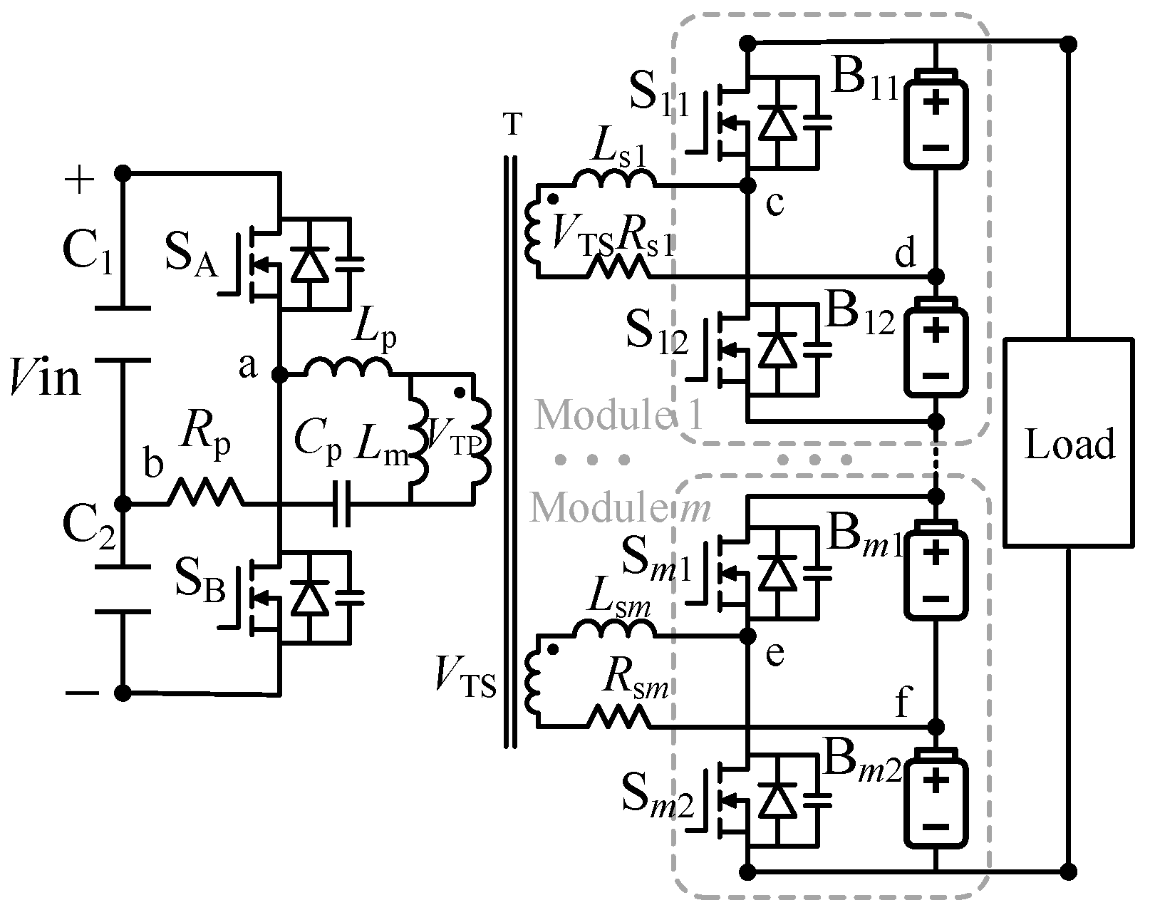
As illustrated in
Figure 1, the proposed voltage-balancing circuit demonstrates two crucial features that enhance its isolation capabilities. Firstly, no direct transmission bus is present between the capacitor and the battery string. Secondly, there is a single connection path between the primary and secondary sides, which is established via a multi-port transformer. The combination of these characteristics substantially improves the isolation effect. The circuit consists of six parts: a multi-port transformer, a half-bridge circuit, a resonant circuit, a rectifier circuit, a battery pack, and the load. Among them, C
1 and C
2 denote support capacitors, and S
A and S
B represent the transistors of the half-bridge. The resonant circuit is composed of a resonant inductance L
p, a resonant capacitor C
p, and a magnetizing inductance L
m. The transistors S
11~S
m2 form
m modules in groups of two. The charging and discharging of 2 m series-connected batteries are achieved through the transformer T.
2.2. Balancing Principle Analysis
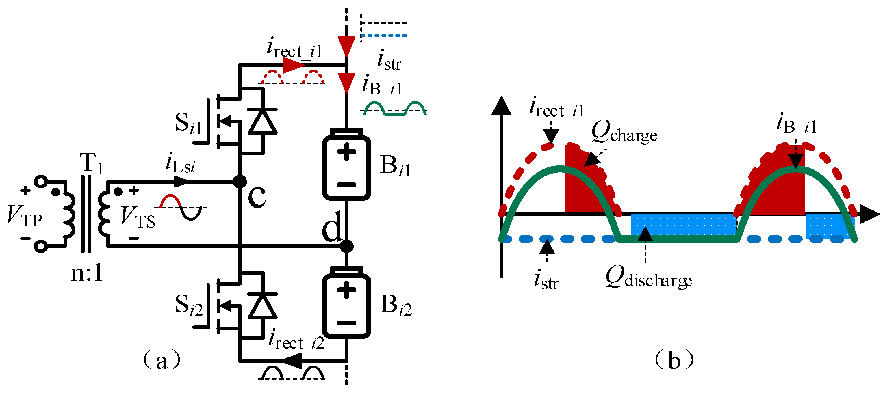
Figure 2 illustrates the voltage-balancing circuit schematic among batteries. Batteries and their corresponding transistors are connected in series in sequence. As illustrated in
Figure 2a, when diodes do not meet conduction conditions, the high-voltage battery’s charging path is cut off. When the switches in Module
i are conducted, the voltage
VTS across the magnetizing inductance is clamped by the voltage
VBi1 corresponding to battery B
i1. At this moment, if
VTS is less than the sum of
VBi1 and the diode drop voltage
VD, then Module
i can remain off. Otherwise, it is forced on, affecting control reliability.
Figure 2b shows the relationship between
VTS and
VBi. A control coefficient
kij is introduced, where
i ∈ {1, 2, …
m} represents the module number and
j ∈ {1, 2} represents the battery position (
j = 1 for upper,
j = 2 for lower). When there is a control signal in the transistor
Sij,
kij = 1, and the battery
Bij is charged; otherwise,
kij = 0, and the battery
Bij discharges.
Neglecting parasitic parameters, the total battery string voltage
Vstr within the effectively truncated module must satisfy the following conditions.
By transformation, the constraint related to the turns ratio
n can be derived as
In Equation (2), the most extreme scenario occurs when the average voltage Vave approaches the maximum single-battery voltage VBmax and the target battery voltage VBij nears the minimum voltage VBmin.
3. Analysis of Equalizing Current
3.1. Analysis of Equalizing Current Characteristics
When the battery voltage
VBij is lower than the average voltage
Vave, the corresponding transistor conducts to charge the corresponding battery. The current
iB_i1 flowing into the battery B
i1 mainly consists of two parts: one is the charging current
irect_i1, showing at most a half-cycle of sine wave per period, and the other is the discharging current
istr, as depicted in
Figure 3.
For a single battery, the charging current
irect_i1 is actually a simplified representation of the current
iLsi1 within a half-cycle. Therefore, the study of
irect_i1 can be transformed into the study of
iLsi1. After introducing the control coefficient
kij, the single-battery charging current
iLsi1 can be rewritten as
According to Equation (3), apart from the control coefficient ki1, the main hardware parameters that affect the current iLsi1 include the damping resistance Req, the resonant Inductance Lp, the characteristic impedance Z0, and the turns ratio n. The voltage parameters include the initial capacitor voltage VCpi10 as well as the distribution of Vave and VBi1. Here, VCpi10 represents the initial value of the voltage VCp corresponding to the resonant capacitor Cp, i denotes the module number, 1 represents the upper position, and 0 represents the initial value.
3.1.1. Influence of Damping Resistance Req on iLsi1
Taking time
t as the independent variable, the curves of current
iLsi1 for different
Req are plotted in
Figure 4a according to Equation (3). With the same parameters, the simulated current waveforms under various conditions are obtained through Matlab R2022b/Simulink, as illustrated in
Figure 4b. Comparison reveals that the peak values of
iLsi1 under identical equivalent resistance
Req differ. In the theoretical current waveform,
Vave and
VBi1 are constant. But in the simulation, capacitor voltage and
VBi1 change with current during operation. Capacitor
C1 discharges, its voltage drops, battery B
i1 charges, and its voltage rises. Thus, the voltage difference across passive components decreases, reducing the peak values of
iLsi1. However, the simulation trend agrees with the theoretical analysis.
3.1.2. Influence of Resonant Inductance Lp on iLsi1
In Equation (3), besides
Req,
Lp also affects the current. When the undamped resonant frequency is constant, different
Lp values change the characteristic impedance
Z0 and the attenuation coefficient. As illustrated in
Figure 5a (theoretical waveform) and
Figure 5b (simulation waveform), the current curves for different
Lp are illustrated. Increasing
Lp raises
Z0, which seems to reduce current. But the attenuation coefficient is inversely related to
Lp, so lower
Lp causes more significant current amplitude decay. Also, higher
Lp makes the circuit’s resonant frequency closer to the undamped one, and the current is closer to a sine wave. Below a certain
Lp threshold, the root-criterion interval of the equation shifts, and the solution form becomes an exponential superposition.
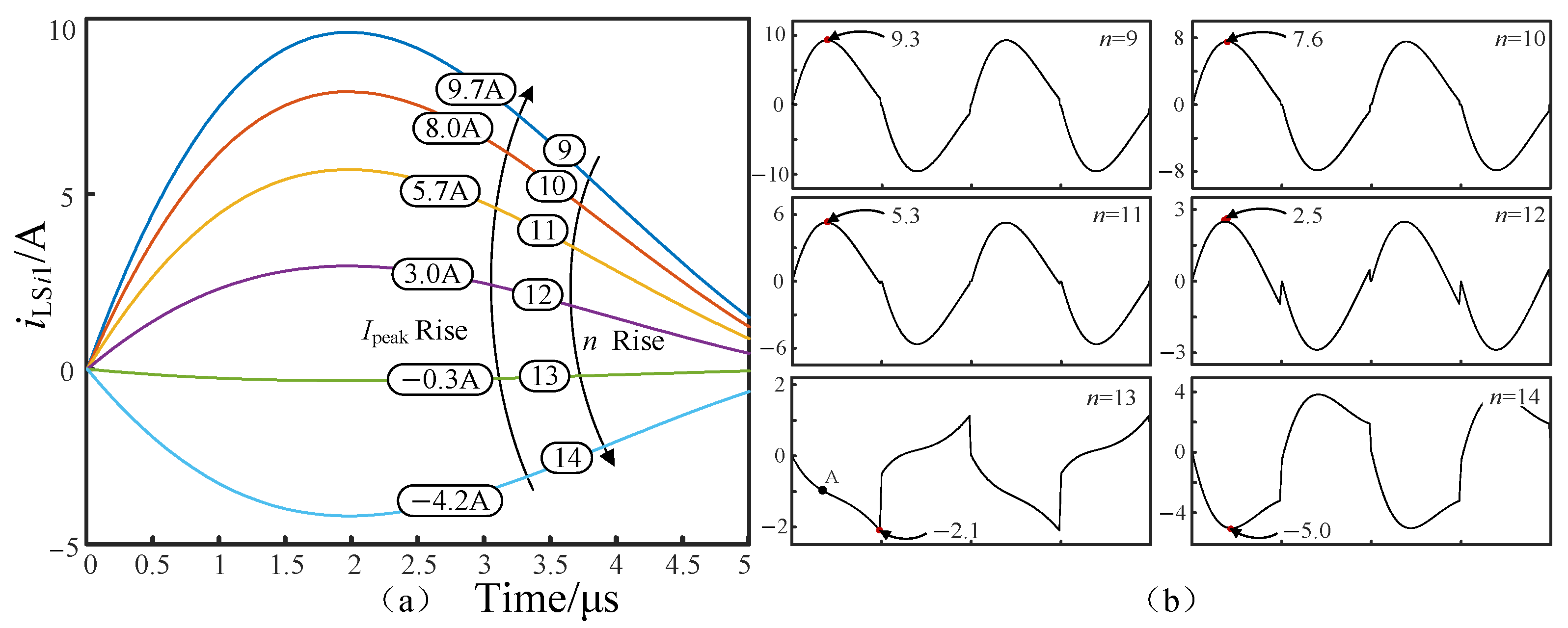
3.1.3. Influence of Transformer Turns Ratio n on iLsi1
The transformer turns ratio
n significantly impacts the equalizing current.
Figure 6 depicts the impact of
n on current
iLsi1, and
Figure 6a,b show theoretical and simulation current curves for different
n. With constant battery voltage, increasing
n decreases the current
iLsi1. Beyond a certain threshold, further
n increases reverse the voltage difference sign and current direction.
When n > 12, a current reversal occurs. At n = 13, the magnetizing inductance voltage is constant. The magnetizing current iLm flows from negative to positive, while the primary-side resonant current iLp reverses and rises slowly, increasing the difference between iLm and iLp. Initially, iLsi1 = 0, and then its negative absolute value grows. The resonant circuit voltage difference is small, with only a resonance tendency (point A), and the peak value of iLsi1 is at the switch-over point. When n = 14, the reverse voltage difference increases, and the resonance is stronger than at n = 13, with the minimum current at the resonance peak.
3.1.4. Influence of the Average Voltage Vave and the Target Battery Voltage VBi1 on iLsi1
When
n is between two turns ratio boundary values of
ndn and
nup, the sign of
iLsi1 depends on the distribution of
Vave and
VBi1. Taking
n = 12 as an example, the
iLsi1 curves against
Vave and
VBi1 can be drawn, as illustrated in
Figure 7. Based on their relationship, the XOY plane can be divided into three regions:
VBi1 <
Vave,
VBi1 =
Vave, and
VBi1 >
Vave. When
n equals the module number
m, if
VBi1 =
Vave, then
nVBi1 =
mVave, the resonant-cavity voltage is zero, the peak value of
iLsi1 is zero, and no energy transfer occurs. If
VBi1 <
Vave, then
nVBi1 <
mVave, the battery-pack voltage is larger, and the peak value of
iLsi1 is positive. If
VBi1 >
Vave, the peak value of
iLsi1 is negative.
During energy transfer, the peak value of iLsi1 is affected by the resonant-cavity voltage difference. With the positive direction from the battery packs to the single battery, the peak value of iLsi1 is maximized when Vave nears its maximum and VBi1 nears its minimum and minimized when Vave is at its minimum and VBi1 is at its maximum. The peak value of iLsi1 is directly proportional to Vave and inversely proportional to VBi1.
3.2. Influence of Parasitic Parameter on Voltage-Equalizing Current iLsi
In practical circuits, parasitic parameters can affect circuit characteristics, degrade performance, interfere with control, or cause circuit failure.
Figure 8 shows the secondary-side equivalent circuit considering parasitic inductance.
After transformation, the total resonant inductance can be calculated as
Lps =
Lp_now +
n2*
Ls. To keep the original undamped resonant frequency and characteristic impedance,
Lp must be reduced to equal the previous
Lp_former. The current
iLsi1 can be derived as
The secondary-side voltage expression can be written as
From Equation (5), VTS is a superposition of multiple voltages. Ignoring the small resistance voltage, compared with VTS without parasitic inductance, the main change is in the inductance voltage. With fixed frequency, the inductance voltage mainly depends on the current amplitude and inductance value.
Based on Equation (5), using
VBi1 and
Lsi as independent variables,
VTS is plotted in
Figure 9a,b. In
Figure 9a, sine
VBi1 affects the resonant-cavity voltage difference, a smaller
VBi1 leads to a larger current peak value and faster current-change rate, resulting in more severe voltage distortion.
The inductance voltage also depends on
Lsi.
Figure 9b illustrates the influence of
Lsi on
VTS. As
Lsi is in-series in the circuit, if
Lp and
Cp are fixed, changing
Lsi affects the characteristic impedance
Z0 and frequency. For decoupling, when
Lsi changes,
Lp should be adjusted synchronously to keep
Lps stable and the current unchanged.
When the distortion causes the peak value of
VTS to exceed
VBi1 +
VD in module
i, the module conducts in uncontrolled rectification, disrupting reliable control, as depicted in
Figure 9c. Under a fixed voltage-equalizing current, the
VTS distortion degree is proportional to
Ls, and a larger
Ls leads to more obvious distortion. Thus, optimizing parasitic parameters and designing hardware parameters to meet reliable control requirements is crucial for better voltage-equalizing performance.
3.3. Design of Key Parameters
In the circuit, the voltage-equalizing current is crucial. At the rated operating frequency, its amplitude is affected by hardware parameters Req, n, Lp, and the distribution of Vave and VBi1.
3.3.1. Transformer Turns Ratio n
Lithium-ion batteries operate at 1.9 V–2.5 V during normal operation. As n changes within this range, the current amplitude can be constantly positive or negative, meaning for a certain n, the circuit’s energy-transfer direction is fixed regardless of battery voltages.
After the battery with an initial energy storage of 0 is disconnected, the upper half-cycle current of a single module is calculated as
At high frequencies, the short switching period makes the exponential term negligible. Substituting
Vstr with
mVave and simplifying, the current amplitude can be obtained as
By solving Equation (7), two boundary values of the turns ratio, namely
ndn and
nup, are obtained as
With a certain margin reserved, the turns ratio n is designed to be 10.
3.3.2. Resonant Capacitor Cp
The resonant circuit consists of
Cp,
Lp, and
Lm. For a fixed-frequency converter, once
Lp is set,
Cp can be deduced from the undamped frequency
fr.
At an operating frequency of 100 kHz, the value of Cp is determined to be 140 nF.
3.3.3. Damping Resistance Req
Req includes primary- and secondary-side line resistances, switch resistance, transformer winding resistance, and battery parasitic resistance. To minimize losses and maximize efficiency,
Req is fixed once the hardware circuit is set. Its constraint is represented by
During the multi-module operation, the number of modules participating in energy transfer changes with the control strategy, and the equivalent resistance Reqm will also change. According to the parallel model, Reqm < Req, so when Req meets the constraints, Reqm does too.
When the frequency is fixed, once Lp is determined, Z0 will also be determined. Therefore, the design of Z0 can be transformed into the design of Lp. Consequently, the design of the current peak value can be achieved by adjusting Lp and n with fixed Req.
3.3.4. Design of Magnetizing Inductance Lm
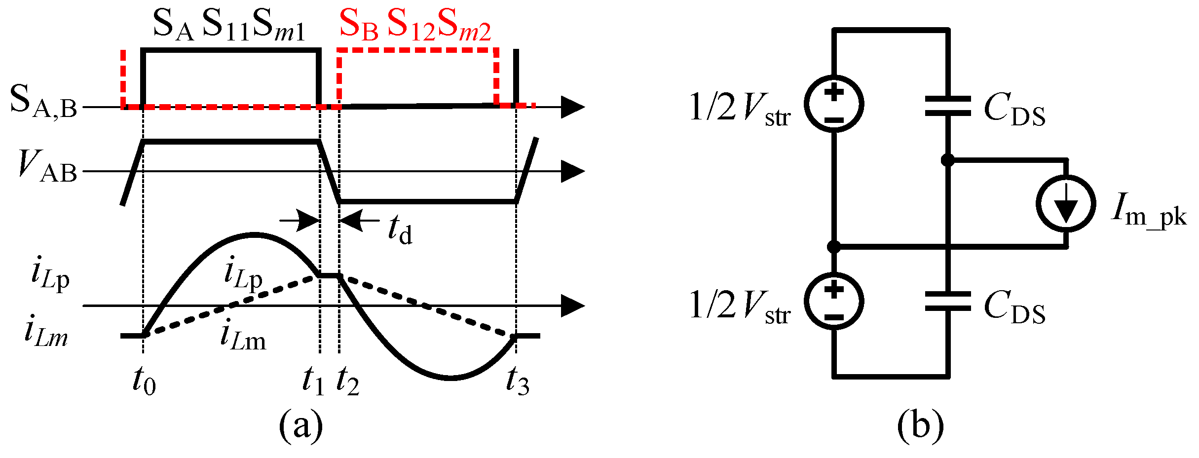
To ensure soft switching, the circuit must operate in the inductive region and meet the parasitic capacitance’s charging and discharging conditions during the dead time
td. The schematic diagram is shown in
Figure 10.
As shown in
Figure 10a, the discharge time of the magnetizing inductance as a current source is actually the dead time
td. The constraint expression to ensure the charging and discharging of the parasitic capacitance
CDS can be written as
In the first half-cycle, when the primary-side transistor is turned on, the magnetizing inductance is connected in parallel with the input voltage
Vin. With constant voltage across it, the magnetizing current rises linearly. Starting from
t0, after a quarter of a cycle, the magnetizing current reaches the maximum value. Therefore, the expression for the magnetizing peak value of
ILm_pk can be written as
By substituting Equation (12) into Equation (11), the constraint for the magnetizing inductance
Lm required for soft switching can be obtained as
Based on these factors, EPC9201 is selected as the switch, featuring an output parasitic capacitance of 1100 pF. For a switching frequency of 100 kHz, the period Ts is 10 μs. A dead time of 100 ns is implemented to prevent short-circuiting between the upper and lower switches. Calculations reveal that the maximum magnetizing inductance for achieving soft switching is 56.8 μH. Since a larger magnetizing inductance results in a smaller magnetizing current and reduced losses during dead time, the chosen magnetizing inductance is set at the maximum permissible value to ensure soft-switching capability.
Based on the above-mentioned parameter design scheme, the final hardware parameters are shown in
Table 1.
4. The Proposed Control Strategy
To equalize all battery voltages to
Vave, a fixed-group-number control strategy is adopted. Primary-side transistors are driven by square-wave signals with a 180°phase difference, and the secondary-side signals are the same. Signals for specific module transistors are determined by the control strategy, with the number of charging modules (
mon) constant during voltage equalization. A block diagram of the fixed-group-number control strategy is shown in
Figure 11.
Step 1: Set the control target. Use voltage standard deviation σ to judge equalization completion. Set control standard deviation target ε and other parameters like total module number (m) and mon.
Step 2: Set PWM signals: Set primary-side PWM signals SA and SB with a 50% duty cycle, the same frequency as the circuit. Block all secondary-side switching-tube signals.
Step 3: Collect data: Collect all battery voltages and group them by module. For the i-th module, the upper-position battery voltage is VBi1 and the lower-position is VBi2.
Step 4: Process data: Calculate the average voltage Vave, range R, and actual standard deviation σ based on the collected voltage data.
Step 5: Judge equalization completion: Compare σ with ε. If σ is less than ε, equalization ends; otherwise, proceed.
Step 6: Battery grouping. Divide all batteries into two groups by the label’s last digit. Group A (odd-numbered) has batteries with labels ending in 1, and Group B (even-numbered) has those ending in 2.
Step 7: Battery sorting: Sort batteries into each group by voltage in ascending order to obtain voltage serial numbers.
Step 8: Set voltage control values: Assign the mon-numbered battery voltage in each group to a register as the control voltage Vmon1 for Group A and Vmon2 for Group B.
Step 9: Compare voltage: Compare each battery voltage in a group with Vave. In Group A, if VBi1 < Vave, proceed; otherwise, apply a zero-level signal to the corresponding transistor. Do the same for Group B.
Step 10: Control PWM signals: Compare battery voltages meeting Step 9 with the control voltage. In Group A, if VBi1 < Vmon1, apply a PWM signal to the corresponding transistor; otherwise, apply a zero-level signal. Do the same for Group B.
After Step 10, continuously check σ. If it meets requirements, block all signals, indicating equalization is complete. If not, repeat steps 3–10.
5. Experimental Verification
To verify the effectiveness and correctness of the proposed circuit and the control strategy, an experimental platform for a 24-series Lithium Titanate Oxide (LTO) batteries was built according to
Figure 1 and
Table 1, as shown in
Figure 12.
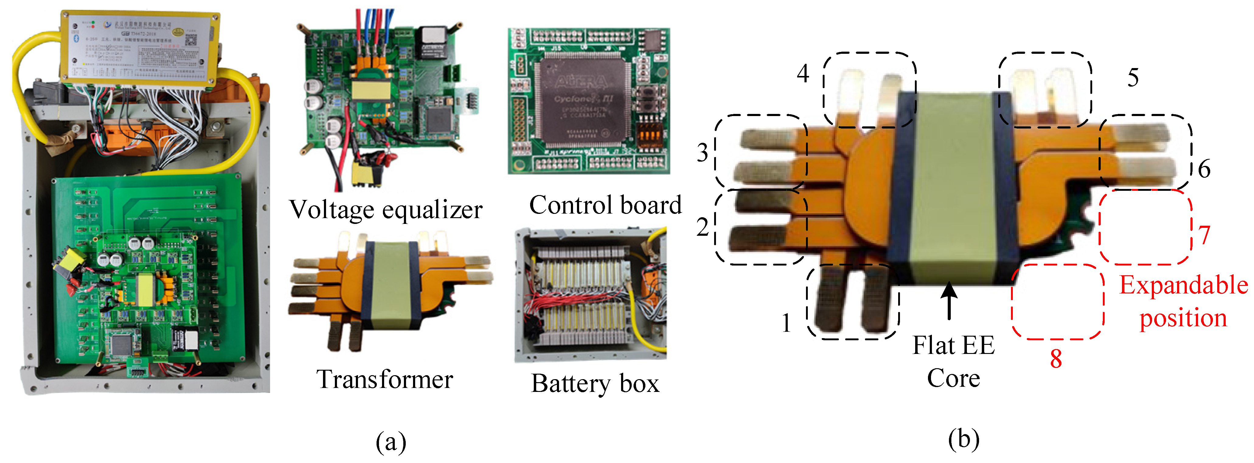
As shown in
Figure 12a, the experimental platform comprises an LTO battery box, a battery interface board, a voltage equalizer, a BMS signal board, and an FPGA control board. The 24-series LTO battery box is for voltage equalization, with a single-cell voltage of 1.9–2.5 V, 15 Ah capacity, and a 100 A charge–discharge current. The interface board shortens lines and reduces parasitic parameters. The equalizer uses GaN Transistors for high efficiency. The FPGA controls switches for energy regulation.
As depicted in
Figure 12b, the designed planar multi-winding transformer has a 10-turn primary of four-layer PCBs and a secondary of double-layer FPCs. With a flat EE core, it can support 32 battery packs with four extra windings at positions 7 and 8. It offers a cost-effective solution by improving the voltage equalization capability and reducing unit cost.
5.1. Soft-Switching Experiment
Figure 13 presents soft-switching experimental waveforms for the complete cycle of a single module (
Figure 13a), the half-cycle of two modules (
Figure 13b), and the complete cycle of two modules (
Figure 13c).
VTS,
iLp,
iLsi, and
iLsj represent the secondary-side voltage, the primary-side equalizing current, and the equalizing current of modules
i and
j, respectively.
In
Figure 13a, when
iLsi = 0, it indicates that neither battery in module
i reaches the equalization condition.
iLsj presents a complete sine wave, which indicates that both batteries in module
j meet the conditions, the upper-positioned battery
Bj1 is charged by the positive half-cycle sine wave with a peak value of 4.5 A, and the lower-positioned battery
Bj2 is charged by the negative half-cycle sine wave with a peak value of 4.9 A. The peak value of
iLp reaches 1.6 A. Through calculation, it can be deduced that apart from module
j, there are still other modules operating.
In
Figure 13b, both modules’ batteries meet the equalization conditions, with each having a half-cycle current per period. The upper-positioned battery in module j is charged by a positive half-cycle sine wave with a peak value of 4.9 A, and the lower-positioned battery in module
i is charged by a negative half-cycle sine wave with a peak value of 5.2 A. Although modules
i and
j are energized for only half a cycle in a single period, the primary-side current still exhibits a complete sinusoidal wave, reaching a peak value of 1.7 A.
In
Figure 13c, The peak value of
iLp reaches 1.8 A. Batteries in both modules meet the equalization conditions, showing the complete sine waves. Each module has a full-cycle current within a single period. The battery in module
j has a lower voltage, resulting in a larger equalizing current with a peak value of 8 A, while the battery in module
i has a higher voltage, leading to a smaller equalizing current with a peak value of 7 A.
As can be seen from
Figure 13, the
VTS waveform is distorted by parasitic parameters, while
iLp is a complete sinusoidal wave, achieving zero-voltage switching (ZVS) in all tested cycles.
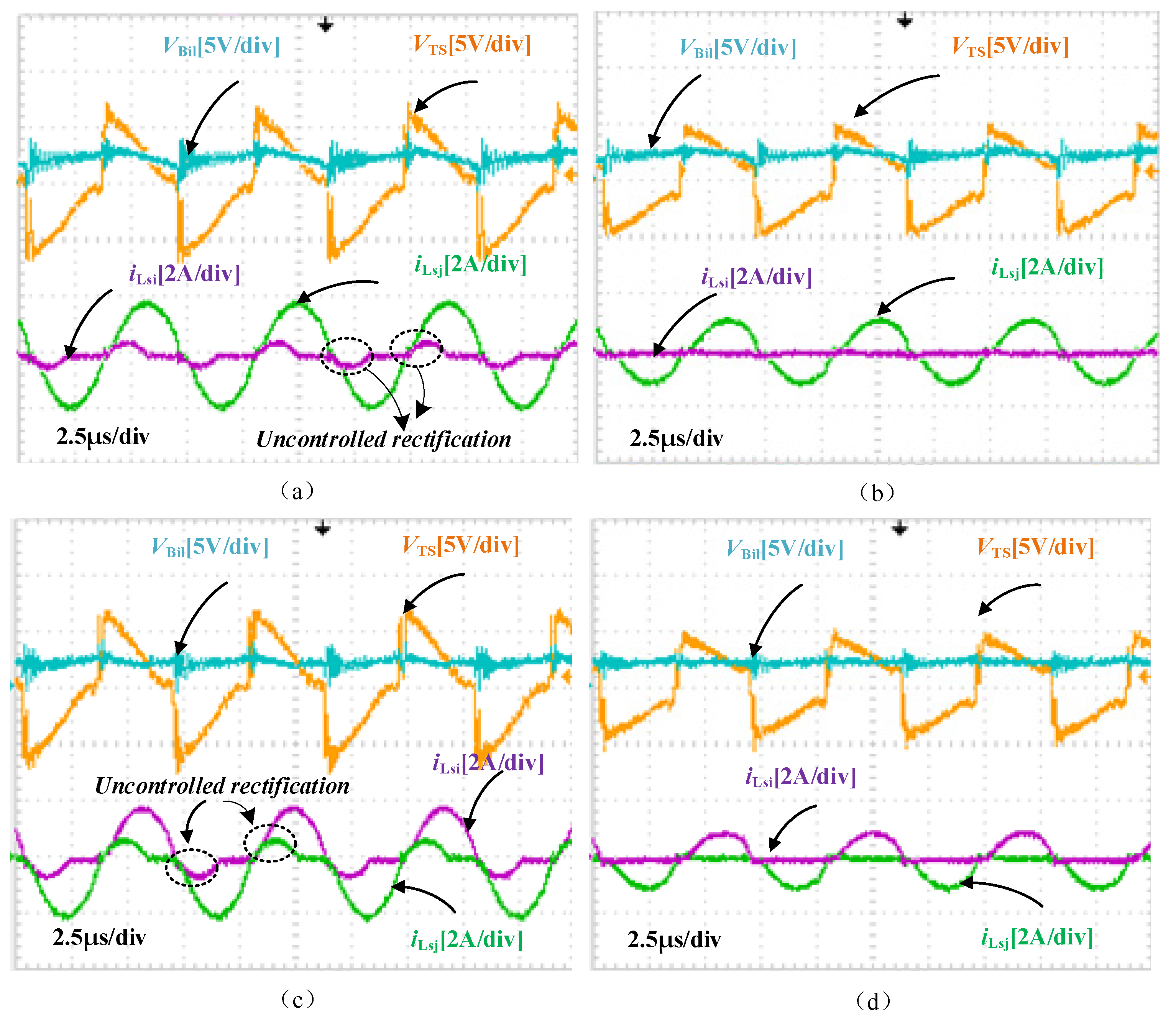
5.2. Parasitic Parameter Experiment
Secondary-side parasitic inductance distorts the transformer’s secondary-side port voltage VTS. When the VTS peak exceeds VBi1 + VD, uncontrolled rectification occurs, disrupting reliable control.
Figure 14 depicts the waveforms before and after optimizing the parasitic parameters. Before optimization, in the complete cycle of a single module (
Figure 14a) and the half-cycle of two modules (
Figure 14c), the parasitic inductance causes the distortion of
VTS. The peak value of
VTS reaches 6.5 V, which triggers uncontrolled rectification. The component-level optimizations primarily focus on minimizing circuit parasitic inductance by reducing the length of transformer windings and the wiring distance from batteries to the equalization circuit. After optimization, in the complete cycle of a single module (
Figure 14b) and the half-cycle of two modules(
Figure 14d), the distortion degree of
VTS is significantly reduced. The peak value of
VTS drops to 4 V, and the uncontrolled rectification phenomenon almost disappears. Experiments show that by optimizing the parasitic parameters, uncontrolled rectification can be eliminated both in the complete cycle of a single module and the half-cycle of two modules.
5.3. Voltage Equalization Control Experiment
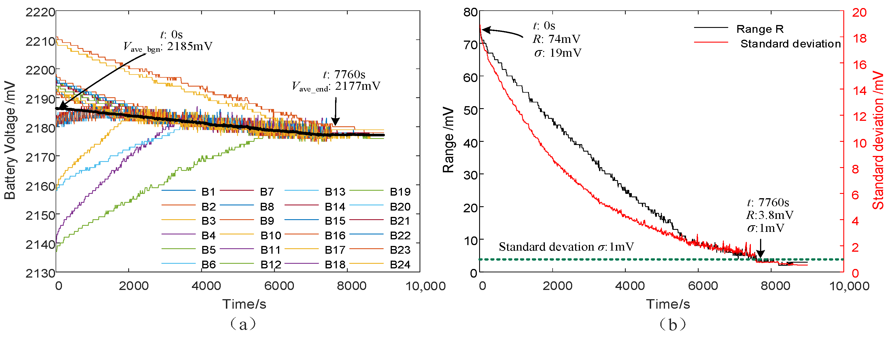
5.3.1. Static Voltage Equalization
The voltage recording graphs and statistical data curves are shown in
Figure 15. At 0 s, the control strategy is applied, and the circuit runs with
mon = 3. The initial average battery voltage, range, and standard deviation are 2185 mV, 74 mV, and 19 mV. By 7760 s, they drop to 2177 mV, 3.8 mV, and 1 mV, meeting the end condition (1 mV standard deviation). When the number of modules needing charging (
mneed) exceeds
mon, the voltage stays around the voltage
Vmon corresponding to the
mon-th battery. Batteries far from
Vmon have stable voltage-curve changes, while those near
Vmon fluctuate. This is because batteries at a relatively far distance have stable charge–discharge states and current directions, with stable internal resistance voltage. In the experiment, the battery pack transferred a cumulative 857 mV over 7760 s, resulting in an energy transfer rate of 0.11 mV/s. Notably, the highest efficiency reached 98.2%.
In
Figure 15a, four batteries have different voltage-rise slopes due to battery module impedance differences. Lower-slope batteries are in high-impedance modules, and higher-slope ones are in low-impedance modules.
5.3.2. Charging Voltage Equalization
The voltage recording graphs and statistical data curves are shown in
Figure 16. At 0 s, the control strategy is introduced with
mon = 6. Initial average battery voltage, range, and standard deviation are 2119 mV, 89 mV, and 29 mV. At 11,420 s, the average voltage and range are 2292 mV and 3 mV, and the standard deviation is 0.8 mV, meeting the end condition. Batteries charge until 11,560 s when the power is cut, with the average voltage reaching 2311 mV. Then, it enters the static stage, and the voltage stabilizes.
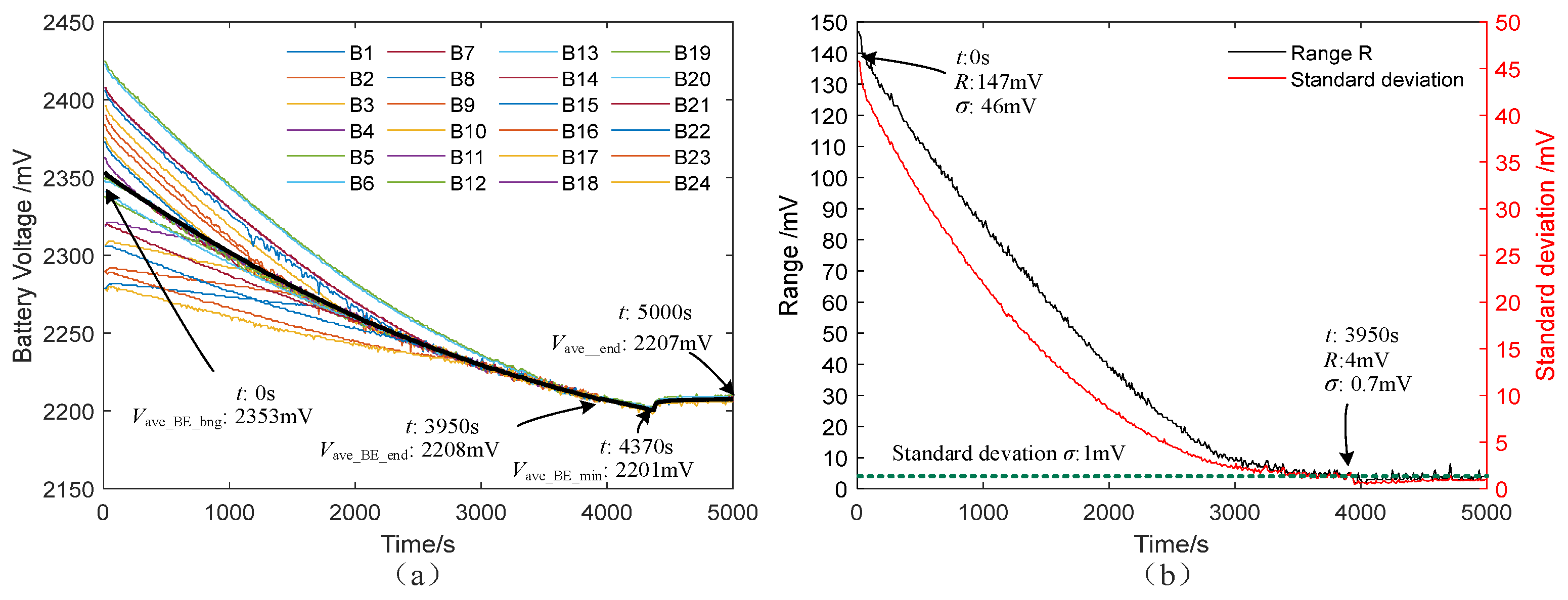
5.3.3. Discharging Voltage Equalization
Figure 17 shows voltage recording graphs and statistical data curves. At 0 s, the control strategy starts with
mon = 6. The initial average battery voltage, range, and standard deviation are 2353 mV, 147 mV, and 46 mV. At 3950 s, they drop to 2208 mV, 4 mV, and 0.7 mV, meeting the end condition. Batteries discharge until 4370 s, with the average voltage at 2201 mV. Then the discharge power is removed, and the system enters the static stage. By 5000 s, the voltage stabilizes.
5.4. Charging and Voltage Equalization Experiment of the Charger
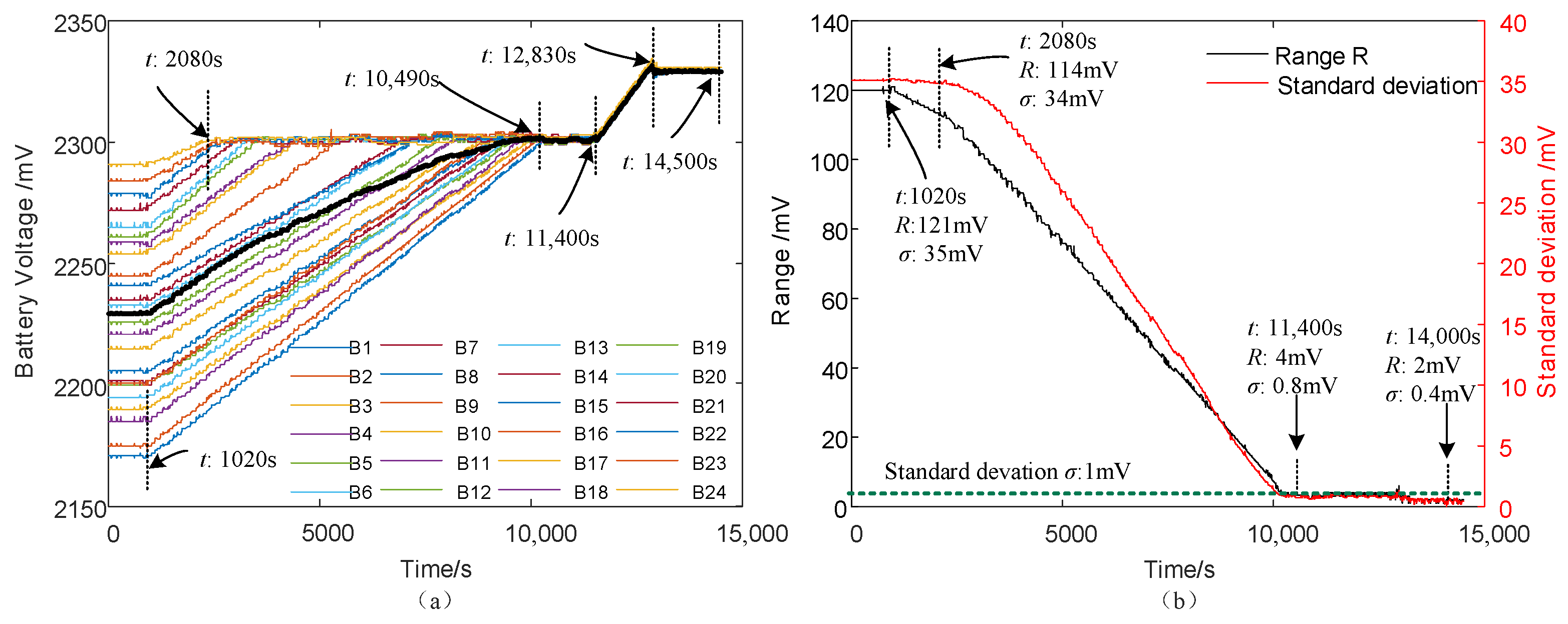
Figure 18 shows the voltage recording graphs and statistical data curves of the charging and equalization experiment of the charger, which consists of five stages. The first stage is the static stage, which lasts 1020 s and has an initial voltage range of 121 mV and a standard deviation of 35 mV. This is followed by the charging and voltage equalization stage, lasting 9470 s with a 3 A current and the number of equalization modules
mon = 6. In this stage, all batteries charge initially, and then high-voltage batteries stop charging at 2080 s while low-voltage ones continue. By 10,490 s, the range drops to 4 mV and the standard deviation drops to 0.8 mV, achieving equalization. Next is the maintenance stage, lasting 910 s, during which the voltage, range, and standard deviation are maintained within the target range. After that, the further charging and voltage equalization stage begins. At 11,400 s, a new target voltage is set, and all batteries charge. At 12,830 s, the power is cut when the target voltage is reached. Finally, the last stage is the static stage again, and at 14,000 s, the standard deviation shrinks to 0.4 mV and the range drops to 2 mV.
The comparison of different voltage-balancing circuits is listed in
Table 2. The proposed circuit and control strategy have full soft-switching operation, high equalization efficiency, large equalization current, the capability to equalize a large number of batteries, and a relatively small number of transistors. Using high-frequency wide-band-gap devices reduces circuit volume and improves overall power density.
6. Conclusions
This paper presents an isolated resonant voltage-balancing circuit based on a multi-port transformer for series-connected lithium-ion batteries. In the proposed circuit, each single battery only requires half a winding and one transistor. The resonant circuit is utilized to ensure that all switching devices can achieve soft switching. The multi-port transformer is employed to increase the equalization current and enable the arbitrary flow of energy among batteries. Notably, there is no direct transmission path between the capacitor and the battery string. As a result, the need for extra switches and control logic is removed, and full isolation is achieved. Additionally, the proposed fixed-group-number control strategy can increase the equalization current, further improving the equalization speed and efficiency. Finally, the designed equalization prototype of a 24-series-connected lithium-ion battery pack verifies the soft-switching performance. The equalization capabilities of the proposed circuit under different working conditions are verified through static equalization, charging equalization, and discharging equalization, with the highest efficiency reaching 98.2%.
Author Contributions
Conceptualization, X.X. and C.C.; methodology, X.X., C.C., and S.J.; formal analysis, X.X., C.C., and S.J.; validation, X.X., C.C., S.J., J.N., and Z.S.; investigation, X.X., C.C., S.J., J.N., and Z.S.; writing—original draft preparation, X.X., C.C., and S.J.; writing—review and editing, X.X., C.C., S.J., J.N., and Z.S. All authors have read and agreed to the published version of the manuscript.
Funding
This research was funded by the National Natural Science Foundation of China (Grant No. 52077183), the High-level Innovation Team and Distinguished Scholar Program of Guangxi Higher Education institutions (Grant Guangxi teach talent [2020] No. 6), the 2024 Guangxi University Young and Middle School Teachers’ Basic Scientific Research Ability Improvement Project (Grant No. 2024KY1151), and Guangxi Vocational College of Water Resources and Electric Power (2023RC01).
Data Availability Statement
The original contributions presented in this study are included in the article. Further inquiries can be directed to the corresponding author.
Conflicts of Interest
The authors declare no conflicts of interest.
References
- Liu, S.; Wang, Y.; Wang, S.; Zhao, W.; Shang, Y. A Compact Large-Current Equalizer Based on Flyback Conversion for Large-Scale Battery Packs. IEEE Trans. Power Electron. 2025, 40, 738–748. [Google Scholar] [CrossRef]
- Cao, Y.; Tian, E.; Chen, H.; Chen, H. Multi-Fault Diagnosis for Series-Connected Lithium-Ion Battery Packs Based on Improved Sensor Topology and Correlation Coefficient Method. IEEE Trans. Autom. Sci. Eng. 2025, 22, 7833–7844. [Google Scholar] [CrossRef]
- Ma, Y.; Luo, W. Research on the Integrated Converter and Its Control for Fuel Cell Hybrid Electric Vehicles with Three Power Sources. Electronics 2025, 14, 29. [Google Scholar] [CrossRef]
- Zhao, Z.; Hu, H.; He, Z.; Iu, H.H.-C.; Davari, P.; Blaabjerg, F. Power Electronics-Based Safety Enhancement Technologies for Lithium-Ion Batteries: An Overview From Battery Management Perspective. IEEE Trans. Power Electron. 2023, 38, 8922–8955. [Google Scholar] [CrossRef]
- Xiao, F.; Wu, L. Personalized Federated Lithium-Ion Battery Capacity Prediction via Cluster and Fusion Modules. IEEE Trans. Transp. Electrif. 2024, 10, 6434–6448. [Google Scholar] [CrossRef]
- Wei, Z.; Peng, F.; Wang, H. An LCC-Based String-to-Cell Battery Equalizer With Simplified Constant Current Control. IEEE Trans. Power Electron. 2022, 37, 1816–1827. [Google Scholar] [CrossRef]
- Li, X.; Chu, J. Lithium Battery Life Prediction for Electric Vehicles Using Enhanced TCN and SVN Quantile Regression. IEEE Access 2025, 13, 12581–12595. [Google Scholar] [CrossRef]
- Nie, J.; Fu, R.; Cai, C.; Ma, J.; Shu, Z.; Ma, L. A High Efficiency Battery Equalizing Circuit Based on Half Bridge Topology With Multiport Transformer. IEEE Trans. Ind. Electron. 2024, 71, 2522–2532. [Google Scholar] [CrossRef]
- Yu, L.; Zhang, Y.; Huang, N.; Zhang, F. An Active Equalization Method of Battery Pack Based on Event-Triggered Consensus Algorithm. Electronics 2024, 13, 151. [Google Scholar] [CrossRef]
- Xiao, H.; Fu, L.; Shang, C.; Fan, Y.; Bao, X.; Xu, X. A Lithium-Ion Battery State-of-Health Prediction Model Combining Convolutional Neural Network and Masked Multi-Head Attention Mechanism. IEEE Trans. Energy Convers. 2025, 40, 218–232. [Google Scholar] [CrossRef]
- Qiao, D.; Wei, X.; Jiang, B.; Fan, W.; Gong, H.; Lai, X.; Zheng, Y.; Dai, H. Data-Driven Fault Diagnosis of Internal Short Circuit for Series-Connected Battery Packs Using Partial Voltage Curves. IEEE Trans. Ind. Inform. 2024, 20, 6751–6761. [Google Scholar] [CrossRef]
- Hasanpour, N.; Mohammadi, M.R.; Tavakoli, A.; Khajehoddin, S.A. Modular Voltage Equalizer Circuit With AC-Bus Inter-Modules Connection. IEEE Trans. Transp. Electrif. 2024, 10, 682–698. [Google Scholar] [CrossRef]
- Manjunath, K.; Kalpana, R.; Singh, B. A Modularized Two-Stage Active Cell Balancing Topology With Reduced Balancing Time for Series Connected Li-Ion Battery String. IEEE Trans. Ind. Appl. 2025, 61, 502–514. [Google Scholar] [CrossRef]
- Rasheed, M.; Hassan, R.; Kamel, M.; Wang, H.; Zane, R.; Tong, S.; Smith, K. Active Reconditioning of Retired Lithium-Ion Battery Packs From Electric Vehicles for Second-Life Applications. IEEE J. Emerg. Sel. Top. Power Electron. 2024, 12, 388–404. [Google Scholar] [CrossRef]
- Yadu, A.; Brahmadathan, S.S.; Agarwal, S.; Sreevatsa, D.B.; Lee, S.; Kim, Y. On-Device Personalized Charging Strategy With an Aging Model for Lithium-Ion Batteries Using Deep Reinforcement Learning. IEEE Trans. Autom. Sci. Eng. 2024, 21, 5037–5047. [Google Scholar] [CrossRef]
- Murillo-Yarce, D.; Colvero, G.D.; Gómez, A.A.; Díaz, J.T.; Rodríguez, A.; Vázquez, A. A Modular Power Converter Topology to Interface Removable Batteries with 400 V and 800 V Electric Powertrains. Electronics 2025, 14, 215. [Google Scholar] [CrossRef]
- Park, S.-J.; Song, Y.-W.; Kang, B.; Kang, M.-J.; Kim, M.-Y.; Choi, Y.-J.; Lim, J.; Kim, H.-S.; Hong, Y. Effect of High-Temperature Thermal Management on Degradation of Li-Ion Battery for Fast Charging. IEEE Trans. Transp. Electrif. 2024, 10, 2912–2922. [Google Scholar] [CrossRef]
- Zhang, R.-P.; Shi, X.-G.; Wei, D.-C.; Wang, Y.-Q.; Yin, W.; Cheng, Y. Multistage Variable Current Pulse Charging Strategy Based on Polarization Characteristics of Lithium-Ion Battery. IEEE Trans. Energy Convers. 2025, 40, 422–436. [Google Scholar] [CrossRef]
- Zilio, A.; Fogagnolo, D.; Gallo, E.; Biadene, D.; Mattavelli, P. A Multiport Converter for Flexible Active Balancing in Li-Ion Batteries. IEEE Trans. Ind. Electron. 2024, 71, 7085–7094. [Google Scholar] [CrossRef]
- Zhang, R.; Wang, S.; Cao, Z.; Chung, H.S.-H. A Galvanic-Isolated Automatic Equalization Charging System for Series-Connected Cells or Battery Strings. IEEE Trans. Ind. Electron. 2024, 71, 13943–13954. [Google Scholar] [CrossRef]
- Xu, B.; Yan, Z.; Xiong, L.; Zhang, L.; Zhou, W.; Mai, R.; He, Z.; Liu, L. A Double-Switch Single-Transformer Integrated Equalizer for the Recycled Power Battery String of Automatic Guided Vehicles. IEEE Trans. Ind. Electron. 2023, 70, 2596–2606. [Google Scholar] [CrossRef]
- Ye, Y.; Huang, P.; Ke, Z.; Wang, X. Multiwinding Transformer Based Cell Balancing System With Cost-Effective Gate Drivers. IEEE Trans. Power Electron. 2025, 40, 2685–2690. [Google Scholar] [CrossRef]
- Uno, M.; Sugaya, R.; Sasama, Y. Selective Module-to-Cell Equalizer With Internal AC Heating Capability for Automotive Lithium-Ion Batteries at Subzero Temperatures. IEEE J. Emerg. Sel. Top. Power Electron. 2023, 11, 5430–5440. [Google Scholar] [CrossRef]
- Milas, N.T.; Tatakis, E.C. Fast Battery Cell Voltage Equalizer Based on the Bidirectional Flyback Converter. IEEE Trans. Transp. Electrif. 2023, 9, 4922–4940. [Google Scholar] [CrossRef]
- Yang, X.; Qi, Y.; Liu, J.; Jia, Z.; Wang, D. Bidirectional Converter Integrating Voltage Equalizer Based on Symmetrical Voltage Multiplier by Sharing a Magnetic Component for Series-Connected Cells. IEEE Trans. Transp. Electrif. 2021, 7, 1074–1087. [Google Scholar] [CrossRef]
- Chen, Y.; Xiao, Y.; Weng, W.; Huang, J.; Weng, Z.; Zou, T. A Multipath Balancing Circuit Based on a Flyback Converter With Battery Switching Units. IEEE Trans. Power Electron. 2024, 39, 15159–15173. [Google Scholar] [CrossRef]
- Wei, Z.; Wang, H.; Lu, Y.; Shu, D.; Ning, G.; Fu, M. Bidirectional Constant Current String-to-Cell Battery Equalizer Based on L2C3 Resonant Topology. IEEE Trans. Power Electron. 2023, 38, 666–677. [Google Scholar] [CrossRef]
- Liu, F.; Zou, R.; Liu, Y.; Wang, Y. A Modularized Voltage Equalizer Based on Phase-Shift Modulation for Series-Connected Battery Strings. IEEE Trans. Ind. Electron. 2023, 70, 12475–12485. [Google Scholar] [CrossRef]
Figure 1.
The proposed voltage-balancing circuit.
Figure 1.
The proposed voltage-balancing circuit.
Figure 2.
The voltage-balancing circuit among different batteries: (a) balancing circuit, (b) relationship between VTS and VBij.
Figure 2.
The voltage-balancing circuit among different batteries: (a) balancing circuit, (b) relationship between VTS and VBij.
Figure 3.
Schematic diagram of battery charging and discharging: (a) equivalent circuit, (b) the current in a single battery.
Figure 3.
Schematic diagram of battery charging and discharging: (a) equivalent circuit, (b) the current in a single battery.
Figure 4.
Influence of Req on iLsi1: (a) theoretical derivation, (b) circuit simulation.
Figure 4.
Influence of Req on iLsi1: (a) theoretical derivation, (b) circuit simulation.
Figure 5.
Influence of Lp on iLsi: (a) theoretical derivation, (b) circuit simulation.
Figure 5.
Influence of Lp on iLsi: (a) theoretical derivation, (b) circuit simulation.
Figure 6.
Influence of n on iLsi1: (a) theoretical derivation, (b) circuit simulation.
Figure 6.
Influence of n on iLsi1: (a) theoretical derivation, (b) circuit simulation.
Figure 7.
Influence of Vave and VBi1 on iLsi1.
Figure 7.
Influence of Vave and VBi1 on iLsi1.
Figure 8.
Analysis diagram of iLsi considering parasitic inductance: (a) equivalent circuit, (b) schematic diagram of voltage and current, (c) equivalent circuit for calculating iLsi.
Figure 8.
Analysis diagram of iLsi considering parasitic inductance: (a) equivalent circuit, (b) schematic diagram of voltage and current, (c) equivalent circuit for calculating iLsi.
Figure 9.
Theoretical waveforms of VTS: (a) influence of VBi1 on VTS; (b) influence of Lsi on VTS; (c) waveform in uncontrolled rectification.
Figure 9.
Theoretical waveforms of VTS: (a) influence of VBi1 on VTS; (b) influence of Lsi on VTS; (c) waveform in uncontrolled rectification.
Figure 10.
Schematic diagram of the soft-switching principle. (a) Waveform of soft switching, (b) discharge path during the dead time.
Figure 10.
Schematic diagram of the soft-switching principle. (a) Waveform of soft switching, (b) discharge path during the dead time.
Figure 11.
Block diagram of the fixed-group-number control strategy.
Figure 11.
Block diagram of the fixed-group-number control strategy.
Figure 12.
Experimental prototype platform: (a) experiment prototype, (b) multi-winding transformer.
Figure 12.
Experimental prototype platform: (a) experiment prototype, (b) multi-winding transformer.
Figure 13.
Waveform of soft switching experiment: (a) complete cycle of a single module, (b) half-cycle of two modules, (c) complete cycle of two modules.
Figure 13.
Waveform of soft switching experiment: (a) complete cycle of a single module, (b) half-cycle of two modules, (c) complete cycle of two modules.
Figure 14.
Waveforms before/after optimizing parasitic parameters: (a) unoptimized in the complete cycle of a single module, (b) optimized in the complete cycle of a single module, (c) unoptimized in the half-cycle of two modules, (d) optimized in the half-cycle of two modules.
Figure 14.
Waveforms before/after optimizing parasitic parameters: (a) unoptimized in the complete cycle of a single module, (b) optimized in the complete cycle of a single module, (c) unoptimized in the half-cycle of two modules, (d) optimized in the half-cycle of two modules.
Figure 15.
Static voltage equalization: (a) voltage recording graph, (b) statistical data curve.
Figure 15.
Static voltage equalization: (a) voltage recording graph, (b) statistical data curve.
Figure 16.
Charging voltage equalization: (a) voltage recording graph, (b) statistical data curve.
Figure 16.
Charging voltage equalization: (a) voltage recording graph, (b) statistical data curve.
Figure 17.
Discharging voltage equalization: (a) voltage recording graphs, (b) statistical data curves.
Figure 17.
Discharging voltage equalization: (a) voltage recording graphs, (b) statistical data curves.
Figure 18.
Experiment of charger: (a) voltage recording graphs, (b) statistical data curves.
Figure 18.
Experiment of charger: (a) voltage recording graphs, (b) statistical data curves.
Table 1.
Main parameters of the proposed circuit.
Table 1.
Main parameters of the proposed circuit.
| Parameters | Values |
|---|
| Number of modules | 12 |
| Number of batteries | 24 |
| Single-cell battery voltage | 1.9 V~2.5 V |
| Single-cell battery capacity | 15 Ah |
| Transformer turns ratio | 10 |
| Transformer magnetizing inductance | 56.8 µH |
| Secondary-side parasitic inductance | 0.1 µH |
| Resonant capacitance | 140 nF |
| Resonant inductance | 18 µH |
Table 2.
Comparison of different voltage-balancing circuits.
Table 2.
Comparison of different voltage-balancing circuits.
| References | Components | Frequency | ZVS | Num. of
Batt | Balancing
Current | Efficiency | Isolation | Size |
|---|
| T | M | C | L |
|---|
| [6] | 1 | 0.5N | 2 | 1 | 200 kHz | Partial | 4 | 0.505 A | 88.1% | Partial | medium |
| [9] | 2 | 4 + 2N | 3 | 2 | 100 kHz | Partial | 12 | 1.8 A | 96% | Partial | Big |
| [12] | 0.5N | 0.5N | N | N | 100 kHz | None | 4 | 0.6 A | 86% | Partial | Big |
| [19] | 1 | 2N + 2 | 2N + 2 | N | 50 kHz | Full | 7 | 0.6 A | 96.3% | Partial | medium |
| [21] | 1 | 0.5N | 2 | 1 | 120 kHz | None | 4 | - | 94.2% | Partial | medium |
| [24] | N | 2N | 2N | N | 29 kHz | None | 4 | 5 A | 90.6% | Partial | Big |
| [23] | 1 | 4 | 4 | 1 | 100 kHz | Partial | 12 | 0.3 A | 92.8% | Partial | Small |
| [25] | 1 | N | 1 | 2 | 100 kHz | Partial | 6 | 0.312 A | - | Partial | medium |
| [27] | 1 | 4 + 2N | 2 | 2 | 16 kHz | Partial | 4 | 0.5 A | 90.1% | Partial | Big |
| [28] | 3 | 2N | 2N | N + 6 | 75 kHz | Partial | 9 | - | 89–91% | Partial | Big |
| Proposed | 1 | 2 + N | 1 | 2 | 100 kHz | Full | 24 | 3 A | 98.2% | Full | Small |
| Disclaimer/Publisher’s Note: The statements, opinions and data contained in all publications are solely those of the individual author(s) and contributor(s) and not of MDPI and/or the editor(s). MDPI and/or the editor(s) disclaim responsibility for any injury to people or property resulting from any ideas, methods, instructions or products referred to in the content. |
© 2025 by the authors. Licensee MDPI, Basel, Switzerland. This article is an open access article distributed under the terms and conditions of the Creative Commons Attribution (CC BY) license (https://creativecommons.org/licenses/by/4.0/).


