1. Introduction
Millimeter wave and Terahertz (THz) waves have gained significant attention for their favorable atmospheric propagation characteristics, rendering them indispensable in diverse fields such as medical imaging, wireless communications, industrial inspection, and security screening [
1,
2]. Despite their vast potential, several challenges impede the widespread adoption of MMW imaging systems, including the lack of reliable and cost-effective detectors, limited sensitivity, complex integration requirements, and slow response times. Existing commercial detectors are often prohibitively expensive [
3,
4], and their operational complexity further increases system cost and limits scalability.
This work proposes a unique solution by exploring the application of Glow Discharge Detectors (GDDs) based on weakly ionized plasma (WIP) technology. Each GDD costs about half a dollar, making them exceptionally convenient for large-area imaging arrays. GDDs exhibit impressive sensitivity to MMW/THz radiation, faster response times, and cost-effectiveness compared to traditional detectors [
5]. Additionally, they demonstrate superior and quicker responses when detecting high-power MMW radiation [
6].
While previous systems often relied on electrical detection modes that required external lock-in amplifiers and complex circuitry, our current FPA design addresses these limitations by integrating a simplified detection system. Specifically, the architecture consists of GDDs arranged in an array, a multiplexer (MUX) for efficient row selection, and direct Fast Fourier Transform (FFT)-based signal processing through a data acquisition (DAQ) platform. By eliminating the need for external lock-in amplifiers, we significantly reduce system complexity, mitigate potential failures due to voltage spikes during GDD switching, and dramatically improve speed, reliability, and cost-effectiveness. This streamlined design offers a practical and scalable solution for real-time millimeter-wave imaging applications.
Building on this foundation, the system integrates Frequency Modulated Continuous Wave (FMCW) radar techniques to further enhance signal analysis and imaging capabilities.
The focus is on harnessing the advantages of GDDs to simplify detection systems and significantly reduce the development cost of MMW Focal Plane Arrays [
3,
4,
5,
6,
7,
8,
9]. Building on the cost-effective GDD-based MMW detection system, this research takes a step further by integrating Frequency Modulated Continuous Wave radar [
9,
10,
11] for enhanced signal analysis and imaging capabilities. GDDs comprise glass envelopes containing an inert gas such as neon with additives to increase ionization efficiency. Two electrodes about a cm long and about a millimeter thick, as shown in
Figure 1, with about a millimeter separation are used for DC bias to break down the gas and create a plasma medium inside the glass envelope. Illumination with MMW/THz waves increases current through ionizing collisions, thus providing electronic detection [
3,
4,
6,
7,
8,
9]. It also increases light intensity emitted by plasma, thus generating up-conversion of the MMW/THz image to visible radiation [
12]. Here, we concentrate on electronic detection.
The GDD can be used as an MMW detector when connected to DC voltage and operating in the abnormal glow regime of the current-voltage (I–V) characteristics. The following
Table 1 summarizes the performance parameters of the existing dedicated THz sensors and points out the benefits of using GDD as an MMW sensor in our experiments.
Each GDD costs about half a dollar, making them convenient for imaging arrays [
5].
Table 2 compares the proposed GDD-FPA system with existing MMW/THz detectors, emphasizing its cost-effectiveness, elimination of lock-in amplifiers, and faster acquisition time. Notably, the system achieves sub-pixel imaging while maintaining noise-equivalent power (NEP) of 3.9 × 10
−10 W/√Hz, competitive with commercial alternatives.
As summarized in
Table 2, the proposed system addresses key limitations of conventional detectors—such as high cost, slow response, and external signal conditioning—while enabling scalable FPA designs for rapid millimeter-wave imaging.
The proposed methodology involves splitting the MMW radiation into two components: the main signal for imaging and a reference signal. To demonstrate the concept in principle, the main signal is directed onto an 8 × 8 Focal Plane Array equipped with GDDs, while the reference signal is focused onto a target object with intentional shape variations. The reflected signals from the object serve as a reference, and the difference in frequencies between the direct and reflected MMW radiation provides crucial range information. This article details the experimental setup, signal processing techniques, and imaging methodology. The integration of FMCW approach aims to overcome the limitations of current MMW detectors, providing a pathway for cost-effective MMW imaging systems with advanced capabilities. The research opens new possibilities for the widespread adoption of MMW technology across diverse domains. Our system, leveraging a Glow Discharge Detector, integrated with a Chirped FMCW radar, offers substantial improvements over existing systems. By eliminating the need for external lock-in amplifiers, and using a simplified detection architecture consisting of GDDs, a multiplexer for row selection, and direct FFT-based signal processing via a data acquisition system, we reduce potential failures due to voltage spikes during GDD switching, significantly simplify the circuitry, and dramatically improve the system’s reliability, cost-effectiveness, and speed, positioning it as a viable alternative for real-time millimeter-wave imaging applications.
2. Methodology and Experimental Setup
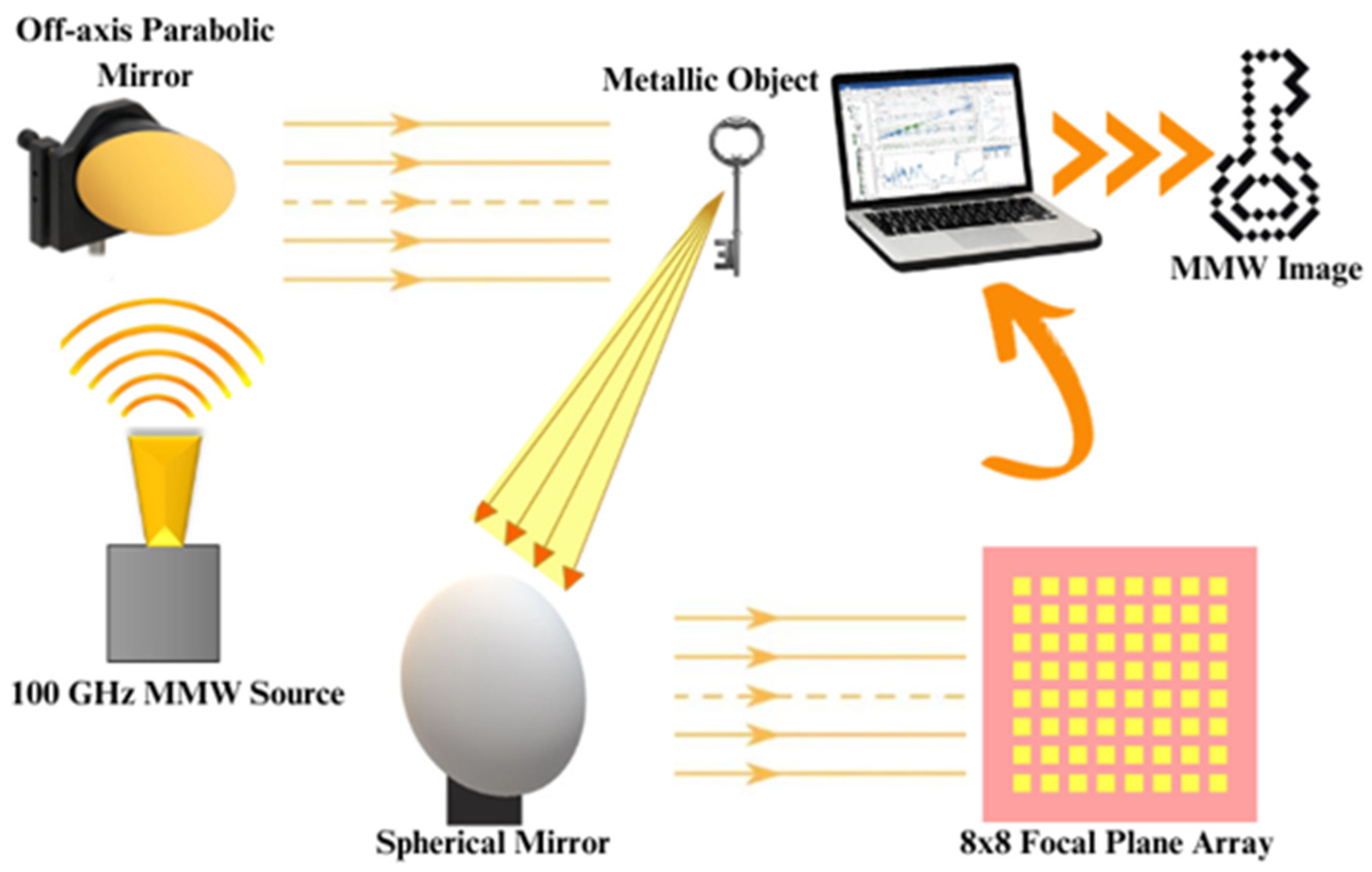
The approach to extending the current single-row detector to an 8 × 8 matrix board entails the establishment of a thorough experimental system, illustrated in
Figure 2. The experimental setup consists of several key components that enable the detection and imaging of millimeter waves using glow discharge detectors as pixel elements. A commercially available MMW source, manufactured by Virginia Diodes Inc. (Charlottesville, VA, USA) (VDI TX272), is employed to provide the MMW radiation necessary for the detection process. The MMW source emits radiation in the desired frequency range and serves as the input signal for the GDD-based detection system.
The MMW source operates at a frequency of 100 GHz, modulated using a 10 KHz square wave with an amplitude of 5 V peak-to-peak. The radiation emitted from the source is first collected by an off-axis parabolic mirror positioned in line with the horn antenna of the radiation source. This mirror collimates the Gaussian beam towards the metallic object placed in the object plane. The reflected MMW radiation from the object is then focused by a spherical mirror, which projects the beam onto the image plane where the GDD-based FPA is located. To ensure precise calibration and alignment of the system, a laser was used to locate the detector array at the reflective focal length of the spherical mirror. The entire design of the imaging system follows a dedicated quasi-optical layout that optimizes the collimation and focusing of MMW radiation onto the detection array, facilitating accurate imaging.
The Focal Plane Array is crafted by organizing an 8 × 8 matrix board and a multiplexer unit for row selection, as depicted in
Figure 3. The FPA board comprises 8 rows, and each of these rows accommodates 8 GDD sensors. In the GDD circuit board configuration, the TLP171D optocoupler was strategically employed for each row, serving as a crucial component for seamless switching operations. These GDD sensors, based on weakly ionized plasma technology, exhibit high sensitivity and fast response times to MMW radiation. The GDDs are positioned with their heads oriented toward the incident MMW radiation, ensuring effective detection along electrode length. This is often preferable to other GDD orientations because of the longer plasma interaction length. In response to MMW incidence, the GDD experiences an additional current surge, signifying the detected signal. This subtle variation in current is then carefully processed, enabling the subsequent stages of signal transformation. The amplifier IC ADA4177-ARZ amplifies the signal, ensuring precise control and stability in the amplification process, with the output representing the enhanced signal from the MMW detection system. This amplified signal plays a pivotal role in the circuit’s holistic purpose. The detection circuit in the FPA converts the detected MMW-induced current variation into a clear and measurable voltage signal. This transformation facilitates efficient reading and subsequent analysis through the data acquisition stage, culminating in a comprehensive and insightful detection mechanism for MMW radiation.
In essence, the circuit acts as a sophisticated translator, converting the subtleties of MMW-induced current variations into a robust and comprehensible voltage signal. The strategic arrangement of the detection circuit is very functional, facilitating efficient detection and analysis of MMW radiation. To prevent excessive heat generation and power consumption from operating all 64 GDDs simultaneously at 100 V DC, a sequential scanning approach was implemented. This method reduces thermal buildup while maintaining system performance by switching through the rows one at a time, ensuring efficient detection without compromising the imaging quality. To facilitate the scanning process and select individual rows to be scanned, an 8:1 multiplexer (MUX) is utilized. The MUX acts as a selector, enabling the sequential scanning of each row of the GDD array. The MUX selection function is performed using an Arduino microcontroller, which controls the MUX by sending appropriate signals to select the desired row. The data acquisition process involves capturing the electrical signals generated by the GDDs in response to the incident MMW radiation. A data acquisition platform is employed to measure and process these signals for further analysis and image reconstruction. The acquired electrical signals from the GDDs are fed into the DAQ system, which computes the averaged Fast Fourier Transform spectrum of the time signals. The FFT algorithm extracts the frequency components present in the signals and provides a magnitude-based representation of the detected MMW radiation. The averaged FFT spectrum serves as the basis for further analysis and image generation. A block diagram of the overall system architecture is shown in
Figure 4 to provide a high-level overview of the signal acquisition and imaging process.
Using the magnitude data obtained from the FFT results, the image reconstruction process begins. For the 8 × 8 matrix board, step motor movements are not required as the entire image can be captured by sequentially scanning each row using MUX and Arduino. The magnitude data from each row is collected and combined to form a complete 8 × 8 pixel image. For larger arrays, such as 16 × 16, 32 × 32, and 64 × 64, the same logic applies. The MUX selection function and Arduino control enable the scanning of each row, while step motor movements are incorporated to perform the necessary translational movements for capturing the complete image. The process is repeated for each row until the entire array is scanned, resulting in the generation of high-resolution MMW images. The entire experimental setup is as shown in
Figure 5.
To validate the functionality and performance of the expanded GDD array and the scanning mechanism, a series of experiments are conducted. The MMW source emits modulated radiation, and the GDD-based detection system captures the corresponding electrical signals. The acquired signals are processed using the DAQ system, and the FFT results are analyzed to evaluate the detection performance and image quality. The performance of the expanded GDD array and scanning mechanism is evaluated based on several factors. These include detection sensitivity, response time, image quality, and cost-effectiveness. Comparative analysis with existing MMW detection techniques and FPAs is conducted to assess the advantages and limitations of the proposed methodology.
3. Imaging Results Analysis Using 8 × 8 FPA
In the captured millimeter-wave images, noise and pixel variations arise from several interconnected factors. One primary source is the variation in reflected signal intensity across different regions of the target object. Even though the MMW beam is collimated using optical elements, energy distribution at different beam spots varies, resulting in non-uniform illumination. Additionally, inconsistencies among individual GDD elements in the FPA contribute to detection variability. Since the GDDs are not commercially fabricated sensors, inherent differences in plasma properties, breakdown mechanisms, and cathode sensitivity regions exist among detectors, despite operating under similar biasing conditions. As a result, the reflected radiation cannot be uniformly focused and detected across all FPA pixel elements, leading to signal fluctuations and image noise. Furthermore, the system’s ability to image all types of metallic objects is fundamentally constrained by the physical resolution limit, determined by the sizes of the imaging optics and the effective pixel area of the detectors. Imaging complex or curved metal objects introduces additional challenges, as finer structural details become harder to resolve with the existing 8 × 8 array configuration. Future improvements—such as enlarging the imaging mirrors and employing smaller cross-section GDDs—would significantly enhance spatial resolution, allowing more accurate reconstruction of intricate shapes and finer surface features.
The implementation of an 8 × 8 focal plane array utilizing glow discharge detectors has demonstrated significant advancements in the acquisition of fast millimeter-wave images with substantially enhanced quality. The experimental results showcased a marked improvement in the speed of MMW image acquisition without compromising on image fidelity or resolution. The FPA system, when subjected to various MMW radiation scenarios, exhibited rapid data acquisition capabilities, capturing images at an accelerated rate while maintaining a heightened level of detail. The primary contribution of our work lies in the development of an 8 × 8 Focal Plane Array utilizing glow discharge detectors, which significantly accelerates the acquisition of millimeter-wave images without compromising image quality. By employing this FPA system, we achieved a substantial reduction in image acquisition time by up to 75%, capturing 8 × 8 images in an average time frame of 4 s. This advancement is crucial for time-sensitive applications such as security surveillance and dynamic object tracking, where rapid and accurate imaging is essential.
To support the enhanced image acquisition, specific numerical values were used for the object and image distances. Initially, both the object distance and the image distance were set at 2 m. Adjustments were made to improve the system’s practical performance: the object distance was reduced to 1.5 m, while the image distance was increased to 3 m. These values were chosen to improve image magnification and thus resolution. The recalculated theoretical resolution limits show an improvement from approximately 0.015 m to 0.011 m due to the adjustments in object and image distances. These numerical values were chosen to enhance the system’s practical performance. The deliberate and precise application of these adjustments demonstrates a significant practical enhancement in image quality. The increased image distance, coupled with a higher magnification factor, results in sharper and more detailed imagery. In conclusion, while the principles employed are based on fundamental geometrical optics, the strategic adjustments in object and image distances, along with the advanced FPA system, have yielded substantial benefits in our imaging system.
The system’s spatial resolution was calculated using the modified Rayleigh criterion [
13]:
where
= 3 mm (100 GHz),
= object distance (1.5 m), and
D = mirror diameter (0.5 m). Optimizing
and image distance (
= 3 m) improved the theoretical resolution from 15 mm to 11 mm, enabling finer detail capture.
Furthermore, the enhancements in the FPA’s sensitivity and resolution were evident in the quality of the acquired MMW images. Comparative analysis between images captured using the enhanced FPA and conventional methods showcased a remarkable improvement in image clarity, finer details, and overall image quality. Notably, the signal-to-noise ratio (SNR) exhibited a notable increase, emphasizing the FPA’s enhanced sensitivity in detecting minute MMW radiation variations. The noise levels of the detection circuit were measured using a spectrum analyzer and found to be 2.1 × 10⁻⁶ V/√Hz. The bandwidth of the amplifier used in the detection circuit, calculated from the frequency response, was determined to be 60 kHz. The effective detection region of the GDD, located between the electrodes and with a diameter of approximately 3 mm, contributed to the system’s improved sensitivity. The total MMW radiation power incident on this cross-section was estimated to be 34 mW, with the detected signal from the amplifier output measured at 740 mV. Hence, the responsivity for the detection system was determined to be 21.8 V/W. The measured value of the Noise Equivalent Power (NEP) was approximately 3.9 × 10⁻¹⁰ W/√Hz, which represents an order of magnitude improvement over previous experimental results. Additionally, the minimum detectable signal power of the system was calculated to be about 0.95 nW, highlighting the system’s enhanced sensitivity. By optimizing the detection efficiency through the use of parabolic reflectors positioned behind each GDD to focus incident radiation onto the region between the electrodes, further improvements in sensitivity and resolution can be achieved.
In our system, the Fast Fourier Transform (FFT) algorithm plays a pivotal role in signal processing by focusing specifically on the 10 KHz modulation frequency, which modulates the MMW radiation source. This selective approach allows the system to filter out all other frequency components, thereby enhancing both the clarity and efficiency of signal detection. By concentrating only on the desired 10 KHz signal, the algorithm significantly improves the signal-to-noise ratio, ensuring more accurate imaging results.
Additionally, the FFT algorithm aids in noise reduction, further refining image quality. Signal acquisition from the detection circuit is performed at a high sampling rate of 100 KHz, capturing 20,000 samples per detection event. This high-resolution data acquisition improves the system’s overall detection capability, allowing for precise and rapid imaging. This method eliminates the need for external signal conditioning, such as a lock-in amplifier, while still providing robust and reliable performance in millimeter-wave imaging.
3.1. Comparative Analysis of MMW Images
To assess the improvements achieved in our MMW imaging system, we conducted a comparative analysis between the image obtained from the current system and that from previous work. In this section, we present a side-by-side comparison of MMW images, highlighting the enhancements in image quality, resolution, and clarity. We first showcase the image obtained from previous MMW imaging system, providing a baseline for comparison. This image represents the state-of-the-art capabilities at the time and serves as a reference point for evaluating the advancements achieved in our system. Next, we present the image captured using our new MMW imaging system. This image demonstrates the improvements achieved through the integration of advanced signal processing techniques, enhanced detector sensitivity, and optimized system configurations. Key features such as finer details, reduced noise levels, and improved contrast are highlighted in these images. The results of the comparative analysis between MMW image from previous work and the one obtained using our enhanced system are detailed in
Figure 6.
The scanned portion of the shape of the object is demarcated within a frame outlined by dotted lines. Outside this marked region, pixel values are evident, indicating the presence of unwanted noise in the acquired image. These extraneous pixel values contribute to the overall noise level and may affect the quality of the image analysis. The deliberate adjustments to the object and image distances have significantly enhanced the image quality, particularly in capturing finer details of the target shape, as per the explanation in
Section 3. This improvement is evident in the second figure despite the presence of some unwanted pixel values, showcasing the system’s ability to resolve smaller features with greater clarity. Additionally, the new approach demonstrates a reduction in the number of unwanted noisy pixels compared to the previous method.
3.2. Enhancing MMW Imaging Results
In the field of millimeter-wave imaging, the accuracy of detecting objects is often hindered by variations in intensity. To address this challenge, an algorithm plays a crucial role in refining MMW imaging results. This algorithm operates on matrices derived from MMW imaging, which include information about the object shape, noise levels, and maximum pixel values from the object. By strategically subtracting noise and normalizing pixel values, the algorithm significantly enhances the quality of the images. This simple yet effective algorithmic improvement is particularly valuable for applications in security systems and industrial inspections where precise detection is of utmost importance.
Within the realm of image processing, an algorithm has been crafted to improve the fidelity of pixel values obtained from MMW imaging. This process involves a sequence of thoughtful steps: loading pixel values from an input source, normalizing these values, and applying histogram equalization to enhance overall contrast. Crucially, the algorithm dynamically establishes a threshold based on the 35th percentile of the equalized values, facilitating effective thresholding. The output is a nuanced progression from the original image to a normalized iteration, further refined through histogram equalization, and culminating in an enhanced image as shown in
Figure 7. This algorithm, marked by its simplicity yet efficacy, bears significant implications for refining MMW imaging outcomes, particularly in scenarios where precision and clarity are of paramount importance.
The algorithm’s effectiveness stems from its hierarchical approach to signal enhancement. First, systematic noise suppression isolates the target signal by leveraging the known modulation characteristics of the MMW source. Next, adaptive normalization preserves relative intensity relationships across the image while compensating for non-uniform illumination. Finally, the dynamic thresholding mechanism automatically adjusts to local contrast variations, ensuring consistent feature extraction across diverse imaging scenarios. This multi-stage processing pipeline balances computational efficiency with perceptual clarity, making it particularly suited for operational environments where both speed and reliability are critical.
The achieved results signify a substantial leap forward in the domain of millimeter-wave imaging, showcasing the FPA’s capability to rapidly acquire high-quality MMW images, setting a promising precedent for its potential deployment across various real-world applications.
3.3. Sub-Pixel Imaging Results: 16 × 16 Image Demonstration
The implementation of a scanning mechanism driven by a step motor has enabled sub-pixel imaging, enhancing the overall system design for millimeter-wave imaging.
Figure 8 illustrates this capability with the result of a 16 × 16 image. Using an 8 × 8 Focal Plane Array, each horizontal and vertical step movement, with a precision step size of 4 mm, effectively creates a 16 × 16 image using only 8 × 8 real pixels. The coordinated operation of the multiplexer selection function and Arduino control facilitates the scanning of individual rows efficiently.
To ensure precise mechanical alignment during sub-pixel scanning, a calibration procedure was implemented using a laser-based reference system. A precision laser was positioned in front of the transmitter horn and directed through the optical path—collimated by the Off-Axis Parabolic Mirror, reflected by the target object, and focused by the spherical mirror onto the FPA. A grid-marked reference sheet was placed at the image plane, allowing visual confirmation of the laser spot locations. By correlating the reflected laser spots with the known grid markings, the linear translational stages were aligned and calibrated to match the designed step size. The motor controller was programmed to perform movements with step sizes equivalent to half the pixel spacing of the 8 × 8 scanning configuration, thereby enabling sub-pixel image reconstruction. This alignment approach ensured accurate positioning, minimized cumulative error during scanning, and validated the repeatability of the imaging process.
This integration not only streamlines the process but also ensures the precise translational movements required for capturing the complete image. The process is systematically repeated until the entire array is scanned, resulting in the generation of high-resolution MMW images. This approach is scalable and can be applied to larger arrays such as 32 × 32 and 64 × 64, further simplifying the process and optimizing time utilization. For larger FPAs, the incorporation of step motor movements allows for capturing intricate details, ensuring the production of high-fidelity MMW images.
These advancements in system design significantly improve the speed and automation of image acquisition, leveraging the inherent advantages of GDD imaging. While not a conceptual breakthrough, these improvements represent valuable enhancements in the practical implementation of MMW imaging systems, providing faster and more detailed imaging capabilities crucial for various applications.
4. Experimental Setup and Measurements for FMCW Radar Detection Using Single GDD Detection Circuit
In FMCW radar systems [
9,
10,
11] operating in the W-band and MMW frequencies, a specialized chirped signal source is essential. Here, we used the chirped radiation source from Virginia Diodes Inc. (VDI), while a signal generator generated a sawtooth signal connected to a voltage-controlled oscillator (VCO) to produce the desired chirped signal. The VCO output frequency corresponding to varying control voltages was meticulously calibrated for accuracy. W-band radiation is efficiently coupled into free space through a conical horn antenna, ensuring optimal transmission for radar detection.
The experimental setup, as depicted in
Figure 9, comprises essential quasi-optical components. A 100 mm off-axis parabolic mirror serves to accurately collimate the FMCW beam, while a free-standing wire grid polarizer (beam splitter) with a diameter of 98 mm precisely splits the beam. One half of the beam is directed to the GDD (reference beam) using mirror 1, while the other half is directed towards a strategically positioned target plate.
Reflections from the metal plate are meticulously redirected to a spherical mirror and then back to the GDD in the single GDD detection circuit, as shown in
Figure 10, effectively serving as the signal beam from the target. This setup allows for comprehensive detection and analysis of MMW radiation. Precise measurements of the full frequency swing (Δf) and time scan (Ts) in the experiment are critical for accurate data acquisition and analysis. The measured values of Δf (6.25 GHz) and Ts (1 ms) provide crucial insights into the behavior of the FMCW radar system under study.
Interpreting Experimental Results
The Optical Path Difference (OPD) is a fundamental parameter in FMCW radar detection, influencing the accuracy and reliability of the measurements obtained. Description of the two possible optical paths of the experimental quasi-optical design is detailed in
Figure 9. By meticulously applying the relevant equations and considering the intricacies of the experimental setup, the OPD is accurately determined. The analysis of experimental results reveals a close correspondence between the measured beat frequency and the calculated OPD, validating the effectiveness of the experimental setup and measurement techniques employed. While experimental results closely align with theoretical expectations, minor discrepancies are noted. These variations are attributed to inherent limitations in range resolution and beat frequency resolution, necessitating careful consideration during data interpretation and analysis.
The OPD directly determines the beat frequency measured in an FMCW radar system. Small inaccuracies in OPD calculation lead to corresponding errors in the extracted distance or range measurements. Since the beat frequency (fb) is proportional to OPD, any error in OPD translates into an error in the estimated distance. Additionally, the system’s spatial resolution is governed by the range resolution formula, indicating that larger frequency sweeps (Δf) result in finer distance resolution. In our setup, the full frequency swing of 6.25 GHz yields a theoretical range resolution of approximately 0.02 m. Therefore, accurate calibration of OPD and careful control of frequency sweep parameters are essential for achieving high-precision millimeter-wave imaging and reliable object localization in future 3D-imaging implementations.
In the experiments conducted for FMCW radar detection utilizing the single GDD detection circuit, several key parameters were measured and analyzed to validate the performance of the system. The VCO, driven by a sawtooth signal from a signal generator, produced a swept frequency ranging from 102.63 GHz at 4.4 V to 108.89 GHz at 7.8 V. These output frequencies were meticulously calibrated to achieve the desired chirp rate and frequency modulation characteristics necessary for FMCW radar operation. Thus, the chirped radiation source was characterized by a full frequency swing (Δf) of 6.25 GHz. The measured Δf and time scan (Ts) were critical parameters in characterizing the FMCW radar system. With a Δf of 6.25 GHz and Ts of 1 ms, the system exhibited a wide frequency sweep and rapid scanning capability, enabling efficient detection and analysis of MMW radiation.
The raw data of the FMCW signal, as illustrated in
Figure 11, were analyzed using a FFT python code that showcase the signal response of the Glow Discharge Detector in the quasi-optical setup with the FMCW method.
In interpreting the experimental results, it was essential to calculate the optical path difference rather than the physical distance traveled by the radiation. Considering that the distance is half the OPD, the measured beat frequency of 69.16 kHz, shown in
Figure 12, corresponded to an OPD of 3.33 m. This value was determined by analyzing the paths taken by the radiation from the source to the GDD, accounting for reflections from the beam splitter and the target plate. While the experimental results closely aligned with theoretical predictions using (2) [
14], minor discrepancies were observed.
In the equation, represents the beat frequency, corresponds to the full frequency swing, stands for the chirp sweep time, ‘c’ denotes the velocity of light in free space, and ‘R’ corresponds to the target range. In FMCW radar systems, this equation is frequently employed to establish the relationship between various operational parameters.
The variations were attributed to limitations in range resolution and beat frequency resolution, which were estimated to be approximately 0.02 m and 1 kHz, respectively, using (3) [
15] and (4) [
16].
where
δR is the range resolution and
δfb is the beat frequency resolution.
Despite these discrepancies, the experimental measurements demonstrated excellent agreement with the expected behavior of the FMCW radar system [
17]. The comprehensive analysis of experimental measurements provided valuable insights into the performance and capabilities of the FMCW radar system utilizing the single GDD detection circuit. By precisely characterizing essential parameters such as frequency swing, time scan, and optical path difference, this study will aid in measuring depths or range, thereby facilitating the generation of 3D MMW images.
To provide a clear overview of the system’s experimental performance, key measurement parameters and observed values are summarized in
Table 3.
5. Limitations of Existing Experimental Configuration in FMCW Radar Imaging
While the experimental setup shown in
Figure 13 utilizing FMCW radar detection with the single GDD detection circuit has shown promising results, several limitations and challenges have been identified, necessitating further refinement and optimization for enhanced performance. One significant limitation arises from back reflections originating from the object under study. In the current quasi-optical setup, reflections from the object may inadvertently strike mirror 1, leading to additional optical paths and the generation of extra beat frequency components. These additional components can introduce noise and interfere with the accuracy of the measurements obtained. Mitigating these back reflections is crucial to ensure the fidelity of the detected signals and the reliability of the imaging process.
Another notable challenge is the uniform projection of the reference frequency component across all pixel GDDs within the Focal Plane Array board. Achieving uniformity in the projection of the reference frequency is essential for accurate and consistent imaging results. However, variations in the projection intensity may occur due to factors such as optical alignment errors or discrepancies in the optical path lengths. Addressing these inconsistencies is paramount to ensure the uniformity and reliability of the imaging process across the entire FPA board.
Prospective Paths and Solutions for Achieving 3D MMW Imaging with FMCW
To overcome these limitations and enhance the capabilities of FMCW radar imaging with the single GDD detection circuit, several avenues for improvement can be explored:
Optimization of Quasi-Optical Setup
Refining the quasi-optical setup to minimize back reflections and stray signals is imperative. This may involve (1) redesigning optical components (e.g., mirror 1) to reduce unintended reflections, (2) implementing servo-controlled mirror angle optimization to dynamically maximize target reflectivity, and (3) integrating parabolic reflectors behind each GDD to focus incident radiation onto the inter-electrode region (where plasma sensitivity is highest). Additionally, anti-reflective coatings on optical surfaces will minimize losses at mirror interfaces.
Uniform Projection Techniques
Implementing advanced projection techniques, such as beam shaping or adaptive optics, can help achieve uniform projection of the reference frequency component across the entire FPA board. By optimizing the distribution of the reference frequency, the accuracy and reliability of the imaging process can be significantly improved.
Integration of Feedback Mechanisms
Incorporating feedback mechanisms and real-time monitoring systems can enable continuous adjustment and calibration of the optical components to maintain uniformity and stability in the projection process. This proactive approach can mitigate variations and ensure consistent imaging performance over time.
6. Conclusions
In this article, we have presented an expansion of the existing single-row detector to an 8 × 8 matrix board with eight rows of glow discharge detectors as pixel elements. By utilizing the advantages of glow discharge detectors, we have demonstrated a cost-effective and reliable solution for millimeter-wave imaging, offering promising applications in various domains. The use of GDDs as low-cost MMW/THz radiation detectors and pixels in focal plane arrays has proven to be advantageous over commercially available detectors. GDDs exhibit high sensitivity and fast response times to MMW radiation, making them an ideal choice for cost-effective detection systems [
1,
6,
7]. By constructing an 8 × 8 matrix board with GDD sensors, we have successfully extended the single-row detector to a scalable FPA configuration.
The introduction of an 8:1 multiplexer and the use of an Arduino microcontroller for MUX selection have enabled efficient scanning of individual rows. This scanning mechanism eliminates the need for step motor movements in generating 8 × 8 images, making the process simpler and more time efficient. For larger FPAs, such as 16 × 16, 32 × 32, and 64 × 64, the same logic can be applied, incorporating step motor movements to capture high-resolution MMW images. The data acquisition system, coupled with the FFT algorithm, effectively processes the electrical signals from the GDDs and extracts the magnitude-based representation of the detected MMW radiation. This approach has proved to be robust and capable of filtering noise, resulting in improved detection signal levels even for extremely low radiation intensities. The obtained MMW images showcase the potential of this low-cost and efficient detection system for various applications. The proposed methodology has several advantages over previous low-cost GDD FPAs, including better responsivity, active overvoltage protection, elimination of the need for external lock-in amplifiers, and faster image acquisition.
Moreover, the integration of Frequency Modulated Continuous Wave (FMCW) radar technology enhances the versatility and capabilities of the MMW imaging system. By incorporating FMCW radar detection, we can overcome limitations such as back reflections from objects and ensure uniform projection of reference frequency components across all pixel GDDs within the FPA board. This opens up new possibilities for achieving ultra-high-resolution MMW imaging and enables more sophisticated image reconstruction techniques.
Our GDD-FPA system achieves breakthrough cost-performance balance, as quantified in
Table 2. While microbolometers offer superior NEP (2 × 10
−11 W/√Hz) and Schottky diodes faster response (1 ns), our solution uniquely combines PCB-compatible integration (
$0.50/unit), μs-scale response, and FFT-based signal conditioning eliminating lock-in amplifiers. This enables <4 s 8 × 8 imaging—75% faster than pyroelectric arrays—making it ideal for real-time security screening.
Looking ahead, the proposed methodology can be further extended to explore even larger FPA configurations, such as 128 × 128 or higher, for ultra-high-resolution MMW imaging. Additionally, the integration of image-processing techniques and advanced algorithms can enhance the capabilities of the MMW detection system, enabling more sophisticated and accurate image reconstruction. In conclusion, the expanded GDD-based FPA, coupled with the scanning mechanism and data acquisition system, offers a cost-effective and reliable solution for MMW imaging. This research presents a steppingstone towards realizing the full potential of MMW technology in addressing pressing societal challenges and advancing the frontiers of modern technology.
7. Future Works
In forthcoming research, our primary focus will be on refining the resolution and sensitivity of the 8 × 8 Focal Plane Array utilizing glow discharge detectors. Efforts will involve exploring novel materials and fabrication techniques to optimize individual detector sensitivity while reducing noise levels. Enhancements in signal processing algorithms will also be pursued to boost sensitivity in detecting millimeter-wave radiation. Simultaneously, we plan to integrate advanced image-processing techniques, such as machine learning algorithms and deep learning architectures. This integration aims to elevate image quality, reduce noise, and improve object detection within captured millimeter-wave data. By amalgamating these techniques, we aim to not only enhance visual quality but also facilitate automated analysis, thereby broadening the FPA’s potential applications across diverse fields.
Moreover, our future endeavors will involve the implementation of FMCW radar technology to achieve 3D MMW imaging, as illustrated in
Figure 14. Our plan includes employing a 2-way power divider in conjunction with two horn antennas connected to the output ports of the divider. This setup aligns well with the specifications and objectives of our project. The utilization of a 2-way power divider will enable efficient distribution of power to multiple components while maintaining signal integrity. This device effectively splits the input signal into two equal parts, facilitating seamless operation across the system. Incorporating horn antennas at the output ports of the divider offers several advantages. Horn antennas are known for their directional properties, providing enhanced gain and coverage in specific directions. This characteristic is particularly beneficial for applications where focused signal transmission or reception is required.
Concurrently, we will pursue system miniaturization through three key strategies: (1) replacement of conventional mirrors with ultra-thin metasurface optics to reduce quasi-optical path lengths, (2) development of monolithic GDD-multiplexer modules using PCB-embedded plasma cavities, and (3) implementation of folded beam paths via kinematic mirror mounts. These modifications target a 50% reduction in system volume while maintaining current resolution thresholds, crucial for field-deployable applications.
Overall, our future works aim to advance the capabilities of the FPA while validating its functionality in real-world contexts, cementing its position as a versatile and efficient millimeter-wave imaging solution adaptable across multifaceted domains.


 ,
, 


