Article

A Linearized Open-Loop MDAC with Memory Effect Compensation Technique for High-Speed Pipelined ADC Stage

State Key Laboratory of Millimeter Waves, Southeast University, Nanjing 210018, China
*
Author to whom correspondence should be addressed.
Electronics 2025, 14(9), 1753; https://doi.org/10.3390/electronics14091753
Submission received: 1 April 2025 / Revised: 19 April 2025 / Accepted: 22 April 2025 / Published: 25 April 2025
(This article belongs to the Section Microelectronics)

Abstract

:
This paper presents a prototype open-loop pipelined stage in a 45 nm CMOS process for supporting 1.8 GS/s and 10-bit design specifications of pipelined ADCs. In order to alleviate the severe non-linearity expressed by open-loop MDACs, an innovative current-mode harmonic compensation is proposed to provide input related third harmonic terms to cancel non-linearity. In addition, an effective double-sampling scheme is optimized by modifying compensation timing and input of a residual amplifier so that the pipelined stage can be immune to memory effect and improve power efficiency. The memory effect compensation scheme can provide a 21 dB improvement on output SNDR of the double-sampling pipelined stage. The simulation results illustrate that the open-loop pipelined ADC stage achieves an output SNDR of at least 52 dB with 840 mV input amplitude and 240 fF load while consuming only 11.24 mW.

1. Introduction

Modern advanced signal processing systems impose higher speed requirements on analog-to-digital converters (ADCs), and pipeline ADCs are the best compromise between speed and accuracy. As a critical component in pipelined ADCs, the settling speed and accuracy of the multiplying digital-to-analog converter (MDAC) seriously affect the performance of the ADC. There are two main problems with traditional closed-loop structures: Firstly, with advancements in CMOS technology, the gate length of MOS transistors has decreased, and supply voltages have also been reduced. As a result, achieving high DC gain directly has become increasingly difficult, which directly affects the linearity related to static error [1,2]. If high DC gain is obtained through an auxiliary gain boosting circuit, it will also increase the power consumption [3]. The second issue is that even though there are many methods available to avoid instability in closed-loop amplifiers, this problem will still become prominent in high-speed application scenarios [4].
Recently, the academic community has proposed many effectively improved MDAC structures. For example, the closed-loop structure-based ring amplifier provides a large slew rate for fast settling while achieving power efficiency [5,6,7]. However, the ring amplifier faces challenges, such as difficulties in the configuration of the dead-zone voltage and relative sensitivity to process, voltage, and temperature (PVT) variations. The research on open-loop MDACs mainly includes two types of residual amplifiers: incomplete-settled and complete-settled. The incomplete-settled residual amplifier significantly mitigates the issue of high-power consumption in pipeline ADCs because it only operates during the amplification phase [8,9,10]. However, due to the correlation between the gain of residual amplifier and the integration time, a shorter amplification phase duration requires a steeper gain-time integration slope. Consequently, the gain error caused by jitter becomes larger. The complete-settled residual amplifier is immune to the aforementioned clock jitter issue; as long as the operation state of the amplifier is established, it is independent of time changes. The main problem for open-loop complete-settled residual amplifiers is that the transconductance Gm, which is purely determined in the voltage domain, varies with signal due to the large-signal characteristics of MOS transistors [11,12,13,14,15]. This problem can be alleviated by either high-order gain calibration or linearization techniques in the analog domain.
In this work, a high-speed, medium-precision open-loop pipelined stage is presented. This open-loop MDAC effectively avoids the risk of instability in high-frequency signal processing compared to close-loop MDAC and can output 8-bit residual signals without any digital correction. Furthermore, it innovatively employs a current-mode compensation technique, which reduces gain sensitivity to process–voltage–temperature (PVT) variations. In addition, the amplifier sharing technique is adopted to improve power efficiency, and the memory effect cancellation method mentioned in this paper avoids the problem of requiring additional long reset times in traditional double-sampling MDACs.

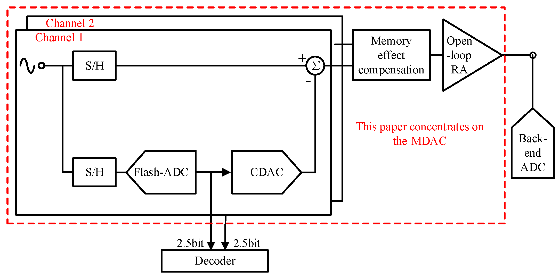
2. Architecture of the Proposed Pipelined ADC Stage

The block diagram of the proposed pipelined ADC stage is given in Figure 1. The complete stage includes a gate voltage bootstrap S/H circuit, high-speed sub-ADC, CDAC, memory charge cancellation circuit, and open-loop residual amplifier. In order to alleviate the accuracy requirement for an open-loop amplifier, the pipelined ADC stage is designed as a 2.5-bit/stage, converting 3-bit output codes that include 1-bit redundancy. As stated in [11], the employment of top-plate sampling for incorporating a reset period can reduce the use of clocks that turn off prematurely, but it will compress amplification time and increase the impact of channel charge injection effects. Since the open-loop residual amplifier is quite sensitive to the input common-mode voltage, the prototype MDAC still employs bottom-plate sampling and is assisted with a memory effect cancellation circuit. In order to meet the requirements of matching and ADC speed, as well as suppress sampling noise in the switched capacitor circuit, the unit capacitance C0 of the CDAC is chosen to be 60 fF, which results in a total differential sampling capacitance of 960 fF for the pipelined ADC stage. The CDAC is constructed in the form of a thermometer code, which determines whether the capacitors in the MDAC are connected to +VREF or −VREF. The final conversion result is transmitted into the residual amplifier after being subtracted from the sampled input signal. The proposed pipelined ADC stage benefits from a linearized design, allowing the residual output to achieve at least 0.85 V of swing under a power supply voltage of 1.2 V.

3. The Open-Loop Amplifier Linearized Through Harmonic Compensation

3.1. Performance Limitation of MDAC

The performance of pipeline ADC is often limited by its first stage. For a pipelined ADC with N-bit total resolution and k-bit per-stage resolution, since the first stage needs to provide a (N-k) bit accurate input signal for the second stage, the precision requirement amplifier can be effectively relaxed due to its 2k gain. For a single pole 2.5-bit/stage MDAC system, the residual output voltages can be given by the following equation:
V o u t = C S A C P + C S V i n A i = 1 8 D i V r e f C i C P + C S 1 e t S B W
where Vref is the reference voltage, tS is the small signal settling time, BW is the main pole bandwidth, and CP and CS are parasitic capacitance and sampling capacitance, respectively. The equation reveals that the error in Vout primarily comprises two components: firstly, the DC gain error in term C S A / C P + C S caused by nonlinearity, and secondly, the dynamic gain error term 1 e t S B W due to small-signal settling errors. Taking the MDAC designed for a 10-bit resolution ADC in this work as an example, and assuming the magnitudes of these two errors are equal, the nonlinear error Δ A / A in DC gain must satisfy:
ε D C = Δ A A 1 2 j + 1 × L S B V F S × 2 k 1 = 0.1953
where Δ A is the DC gain error, L S B V F S = 1 2 N , and j is the additional peak-to-peak DNL/INL accuracy required for the quantization margin; if the additional requirement is 0.5 LSB, then j is 1.
Similarly, the amplifier’s allowed settling error needs to be:
ε s e t t l e = e t S B W 1 2 j + 1 × L S B V F S × 2 k 1
Therefore, when the settling time tS needs to be less than 450 ps, the required bandwidth can be calculated as BW = 2.206 GHz. However, since a typical MDAC is a multi-pole system, the actual required bandwidth will be higher. With the limitation of linearity and bandwidth, we have the specifications needed to design the MDAC’s amplifier.

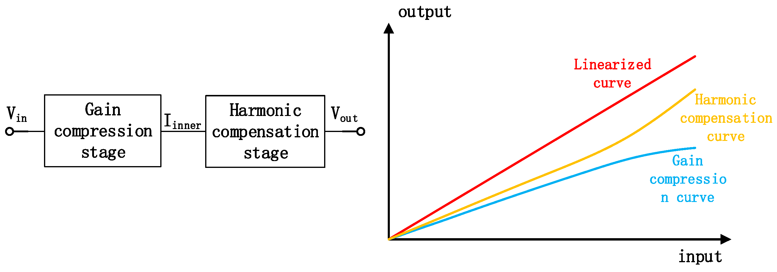
3.2. Amplifier Linearity Analysis

An effective method for linearizing the voltage amplifier utilizing post-correction is shown in Figure 2. The main design idea is to consider the two-stage amplifier as a cascade of a V-I converter and an I-V converter, where the two converters have opposite curvature variations. It allows the compressed linearity to be well-corrected.
As shown in [15], traditional operational amplifiers exhibit compressing V-I characteristics due to the limitation of the fixed tail current source. Therefore, the linearization design discussed in this paper primarily focuses on the I-V module. Any MOS transistor integrated in a circuit will cause nonlinearity due to its channel modulation effect and the variation of gm with the input. Now, if the large-signal model of a Gm unit with third-order nonlinearity is expanded in polynomial form, the V-I characteristics can be obtained:
I o u t 1 = a 1 V i n 1 a 3 V i n 1 3
V o u t 2 = b 1 I o u t 1 + b 3 I o u t 1 3
where a1 and a3 have the same polarities, and a1 represents the equivalent transconductance of the first stage, and a3 indicates the compressing characteristic of the V-I transfer. Similarly, b1 represents the equivalent transimpedance of the second stage, and b3 is the Nonlinear coefficient of the second stage. The corrected output voltage can be obtained by substituting Equation (4) into Equation (5):
V o u t 2 = a 1 b 1 V i n 1 ( a 3 b 1 a 1 3 b 3 ) V i n 1 3 3 a 1 2 a 3 b 3 V i n 1 5 +   3 a 1 a 3 2 b 3 V i n 1 7 a 3 3 b 3 V i n 1 9
where A = a1b1 is the target gain for the amplifier design and ( a 3 b 1 a 1 3 b 3 ) is the total third-order nonlinearity at the amplifier output. To ideally cancel the effect of the original a 3 V i n 1 3 , b1 and b3 need to satisfy:
( a 3 b 1 a 1 3 b 3 ) V i n 1 3 = 0
thus, obtaining the ideal values for b1 and b3:
b 1 = A a 1 b 3 = a 3 A a 1 4
In practical design, since a1 has an impact in the form of a square in the fifth-order term of 3 a 1 2 a 3 b 3 V i n 1 5 , a1 is set slightly smaller, while b1 is set slightly larger.

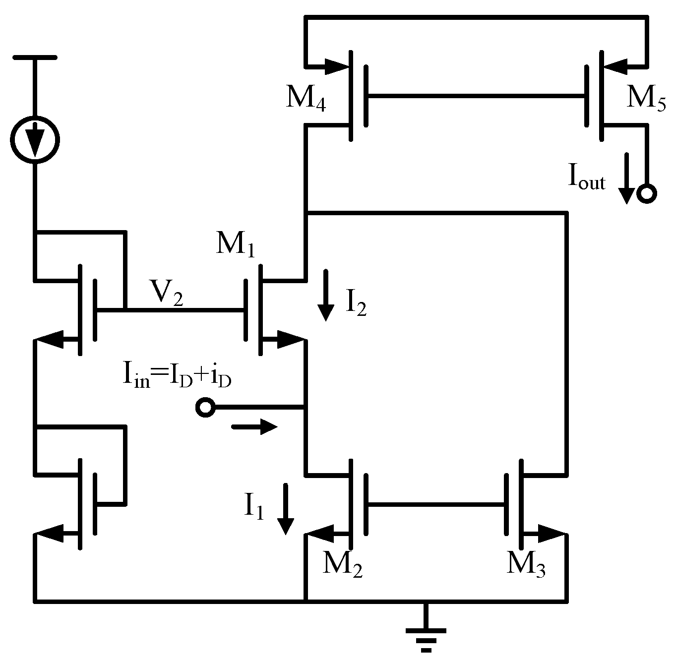
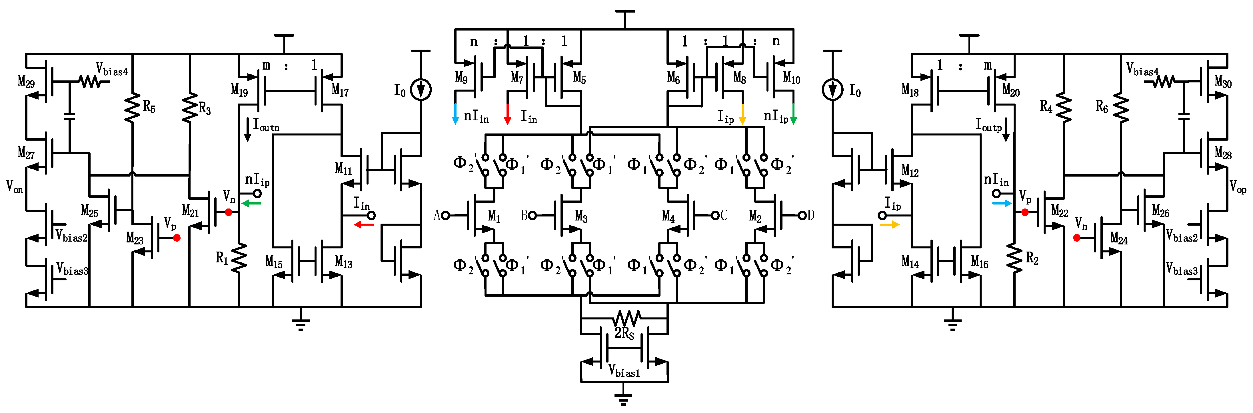
3.3. Current-Mode Harmonic Compensation Circuit Design

From the above analysis, it can be seen that in order to cancel the nonlinearity of the third-order term, a positive b3 is required. Since it is difficult to directly obtain a cubic current signal in CMOS circuits, a method of obtaining the cubic term through two successive current squaring circuits is considered in this work.
To reduce additional nonlinearity caused by unnecessary MOS transistors, the current squaring circuit needs to use the simplest structure to obtain reliable squared current signals. The current square circuit [16] shown in Figure 3 is used in this paper. Under the conditions of the large-signal model, assuming that the input current, which is the output current of the first stage Iin = ID + iD, where ID is the fixed DC current part and iD is the AC current part., then, the output current Iout is given by:
I o u t = m [ 2 I 0 + ( I D + i D ) 2 8 I 0 ]
In Figure 3, m is the current mirror multiplication factor, and I0 is the bias current. To obtain a positive cubic term, the mirrored first-stage output current nIin in Figure 4 must be subtracted from Iout:
I o u t n I i n = I o u t n ( I D + i D )
However, such current subtraction requires additional current steering circuits, which inevitably increases the power consumption of the circuit and introduces non-ideal effects. Therefore, by utilizing the symmetric property of the differential circuit, the output current Iout of the first current squaring circuit is added with the mirrored current from the other side of the original first-stage output. In this case, we have:
I o u t + n I i n = I o u t + n ( I D i D )
and expanding this expression gives:
I o u t + n ( I D i D ) = m i D 2 8 I 0 + ( m I D 4 I 0 n ) i D + 2 m I D + m I D 2 8 I 0 + n I D
From the above equation, it can be seen that the constant term must be positive, and the necessary requirement for the compensation design is that m/8I0 and (mID/4I0n) have opposite symbols. If the first-stage nonlinearity of an open-loop amplifier requires significant compensation, a larger n should be necessary to obtain a larger positive cubic term in the final compensation result.
For simplicity and to ensure sufficient gain, the second current squaring circuit adopts a common-source amplifier structure, as shown in Figure 4. The current signal is firstly converted into an equivalent voltage signal before performing the squaring operation. In order to achieve better squaring property to improve compensation capability, the common-source transistor M1 needs to operate near the subthreshold region, and the size of M1 must be carefully chosen as a compromise due to bandwidth issues. Since the second squaring circuit is a simple common-source structure, it introduces inherent nonlinearity to this configuration, which degrades the overall harmonic compensation efficiency. Therefore, transconductance compensation is applied to M1 by using another transistor M3 working in class-C to compensate during large output swings. Vp and Vn are the voltages of the corresponding nodes in the differential circuit.
The result of the second squaring and unfolding of the current I o u t + n I i n = I o u t + n ( I D i D ) is:
k n I o u t + n ( I D i D ) R 1 V T 2 = k n 2 m 8 I 0 m I D 4 I 0 n R 1 2 i D 3 + 2 V T R 1 m i D 2 8 I 0 + ( m I D 4 I 0 n ) i D + 2 m I D + m I D 2 8 I 0 + n I D + V T 2
where kn is the inherent parameters of transistors, and VT is the threshold voltage of M1. In Equation (10), the third-order current component I = 2 k n m 8 I 0 m I D 4 I 0 n R 1 2 i D 3 will exhibit positive polarity after being reconverted to voltage through V o u t = V D D I R 2 .
The entire current-mode harmonic compensation circuit uses NMOS transistors as much as possible, so most transistors exhibit similar mobility variations across different process corners, resulting in a more stable compensation effect.

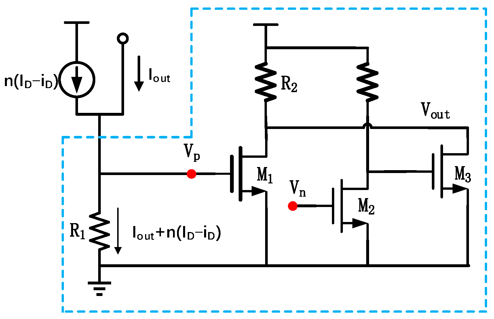
3.4. First-Stage Amplifier

The first-stage amplifier employs the simple differential source degeneration structure shown in Figure 5. The first stage requires a trade-off between bandwidth, gain, and linearity during the design. The transconductance of this stage can be figured from the following equation:
G m = g m 1 + g m R S
A larger Rs would improve linearity but would also lead to a decrease in Gm, as well as a decrease in the dominant pole and gain. Therefore, in this work, Rs does not need to be very large; it only needs to alleviate the pressure on the current-mode harmonic compensation stage. In summary, Rs is set to 1.38 kΩ in this work. On the other hand, due to the high precision requirements of the first-stage CDAC, which is susceptible to the parasitic capacitance at the input of the amplifier, the gain of the first-stage amplifier should not be set too large. In this design, the gain of the first stage is approximately 1.2.

3.5. Open-Loop Amplifier with Current-Mode Harmonic Compensation

The overall two-stage open-loop amplifier structure is shown in Figure 6. In order to drive the large sampling capacitor of the subsequent pipelined stage, an additional buffer is added. The total gain of the amplifier is 4.466, which will be corrected with CDAC gain calibration [11,14] to achieve an inter-stage gain of about 4. The static current of this design is 5.88 mA, resulting in a power consumption of 7.056 mW for a single amplifier.
Employing conventional noise analysis techniques allows us to show how input referred thermal noise density is approximately given by the following expression:
V n , i n 2 ¯ = 4 K T [ γ g m 22 2 R 2 R 4 + γ g m 22 R 2 + 1 R 2 + γ ( g m 9 + g m 22 ) m 2 ( g m 2 g m 2 R S + 1 ) 2 + γ ( g m 18 + g m 8 + g m 4 + 2 g m 16 ) + g m 2 2 R S ( g m 2 R S + 1 ) 2 ( g m 2 g m 2 R S + 1 ) 2 + γ g m 2 ]
where k is the Boltzmann constant, and γ is the process-dependent noise coefficient. From the above analysis, the most effective method to reduce the overall noise of the amplifier is to increase the small-signal transconductance of MOS transistors M2 and M22, and to increase the current scaling coefficient m, while decreasing the small signal transconductance of M4, M8, M9, M16, and M18.

4. Memory Effect Compensation

4.1. Memory Effect Analysis

All multiplexing sampling systems are inevitably affected by the memory effect, and pipelined ADCs operating in double-sampling mode are no exception. When only considering the influence between adjacent phases, the output voltage of a conventional double-sampling system, as shown in Figure 7, which includes inter-channel crosstalk in each cycle [17], can be expressed as:
V o u t 2 = V o u t 1 A C p C s + C p A C s V i n 2 C p C s + C p A C s
where Cs and Cp are the sampling capacitor and input parasitic capacitor of the amplifier, respectively, A is the open-loop gain of the amplifier, and the term containing Vout1 represents the memory effect interference. It can be seen that the magnitude of the inter-channel crosstalk in the output of conventional closed-loop sampling systems is greatly influenced by the open-loop gain A. Therefore, the memory effect can be attenuated with a large DC gain of the op-amp and small parasitic capacitance. However, for the same Vout1, the inter-channel crosstalk has more severe impacts on Vout2 in an open-loop MDAC, because of the relatively low amplifier gain; therefore, a precise compensation scheme is necessary.

4.2. Memory Effect Compensation Scheme

The most ideal and simplest way to eliminate crosstalk caused by memory effects is resetting, but inserting an additional reset phase would significantly reduce the time available for the amplification phase because of the particularity of double sampling. In order to avoid occupying time from the amplification phase, this work adopts a memory charge cancellation technique.
The pipelined ADC stage implemented based on this scheme is shown in Figure 8. The timing logic is shown in Figure 8b, where Φ1′ and Φ2′ control the memory effect cancellation for channel 1 and channel 2, respectively. Figure 8c illustrates the configuration of input terminals of the improved open-loop amplifier. The input transistors of the conventional open-loop amplifier are split into four parts: A, B, C, and D, each with a size equivalent to half of the original. The four input terminals are alternately paired in two adjacent amplification phases to achieve memory charge cancellation at the input of the amplifier.
During phase Φ2, channel 2 samples the signal onto Cs, while the residual signal generated at the end of the previous phase Φ1 is amplified in channel 1 and simultaneously charges the input parasitic capacitance of the amplifier. Since the amplifier operates in fully differential mode, the charges stored on the capacitors at terminals A, B, C, and D of the amplifier are opposite polarity, and the charge amounts are assumed to be +Q and −Q, respectively. In the subsequent Φ1 phase, the amplifier input terminals B and C are switched to paths opposite to those in the Φ2 phase before the residual signal of channel 2 is amplified. The charges stored on the input capacitors of terminals A and C have opposite polarities but equal amounts, thus, the memory charge will be canceled out. The same effect also occurs at terminals B and D.
The memory effect in open-loop pipelined ADC with double-sampling is more severe compared to that in a closed-loop structure. By advancing the memory effect compensation control signal to a brief period before the actual turn-on moment of the amplification phases Φ12, charge cancellation can be performed prior to inputting the residual voltage of the corresponding channel, thereby further improving the accuracy of compensation. On the other hand, the switch configurations for each of the amplifier input terminals A, B, C, and D are set to be identical, which minimizes differences in input parasitic capacitance Cp between the terminals. This method prevents incomplete charge cancellation caused by input capacitance mismatch.

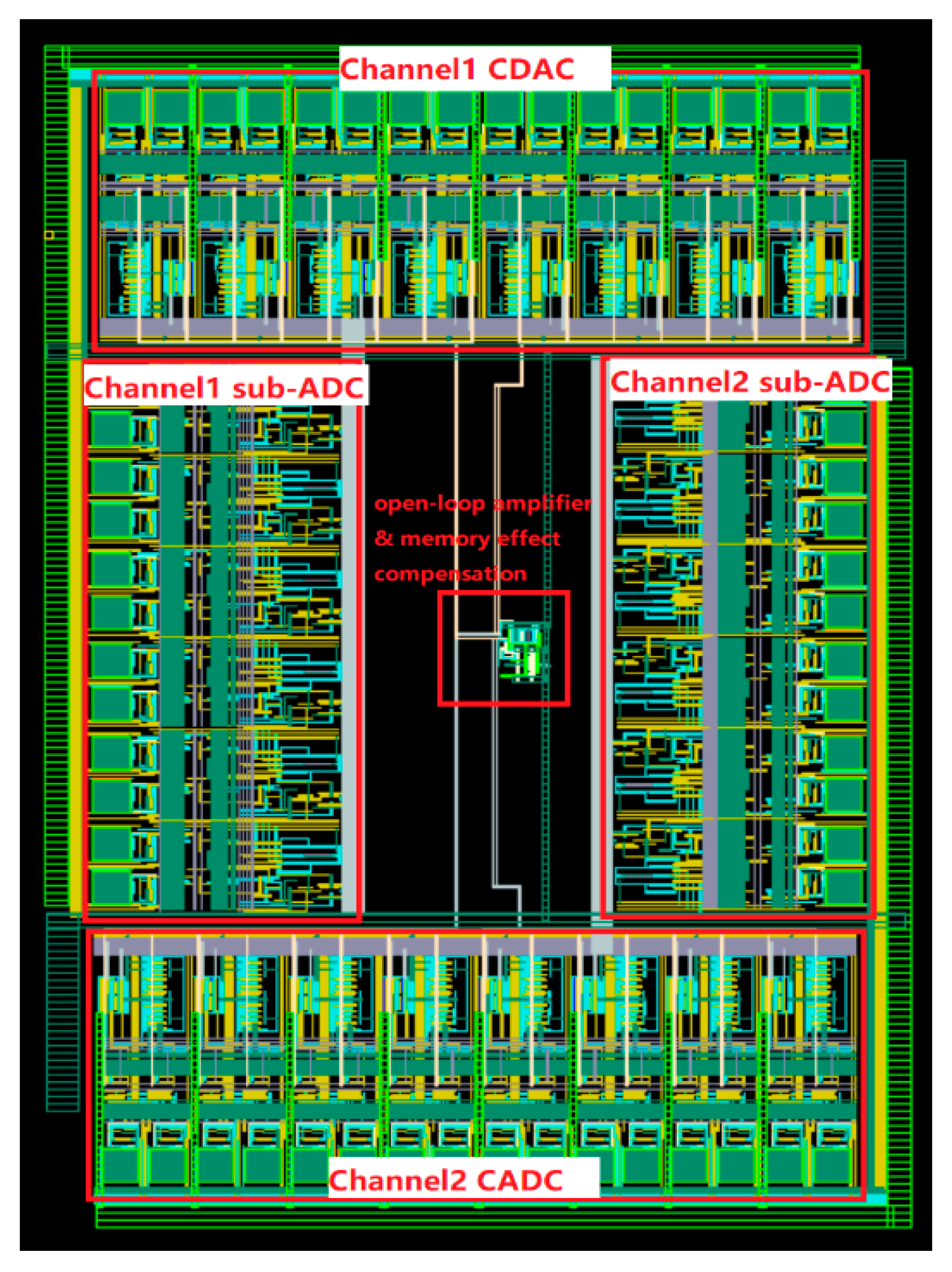
5. Simulation Results

The pipelined ADC stage based on an open-loop structure is manufactured in 45 nm CMOS technology. The layout of the pipelined ADC stage is shown in Figure 9, and it includes gate voltage bootstrap S/H circuits, a double-sampling MDAC, and a high-speed dynamic comparator in a fully differential structure. Each module is carefully laid out to minimize mismatch, and the occupied area of the proposed ADC stage is 0.06 mm2.

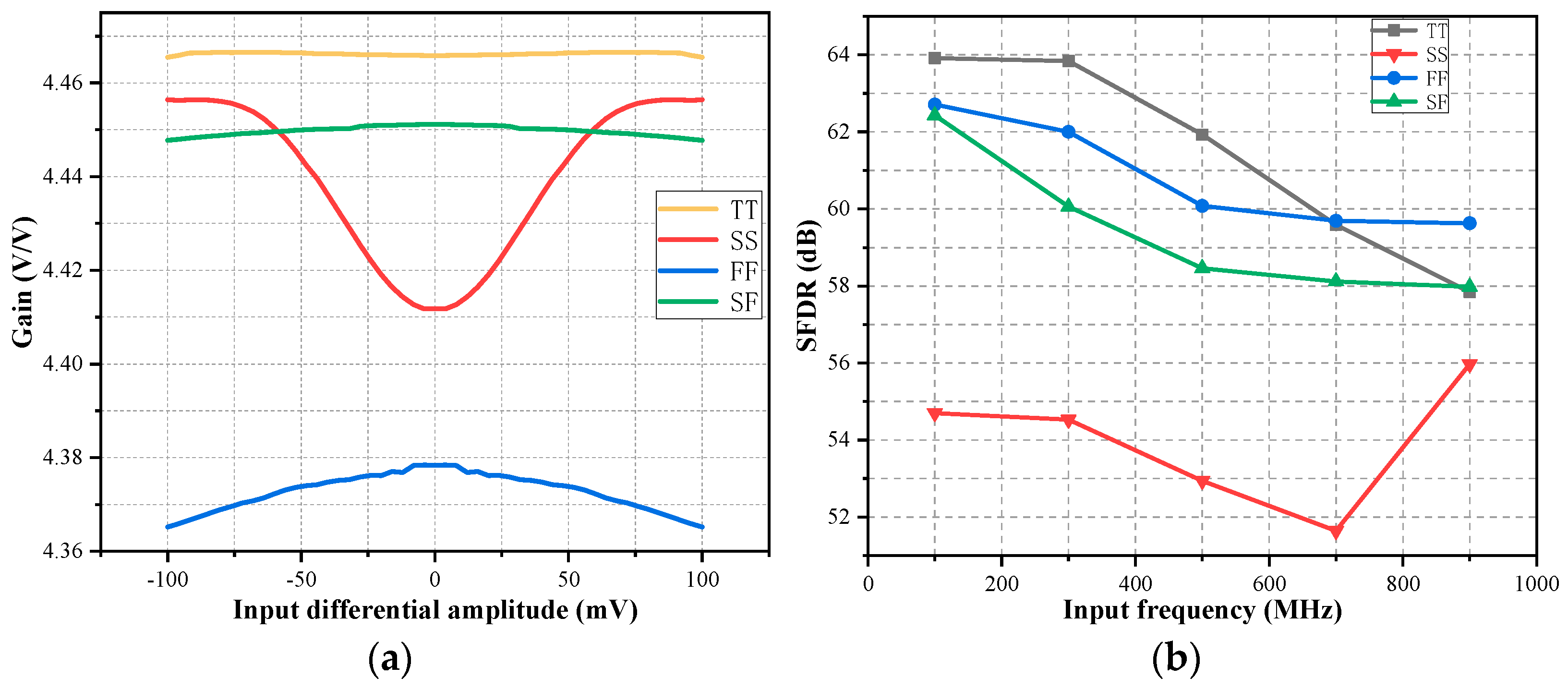
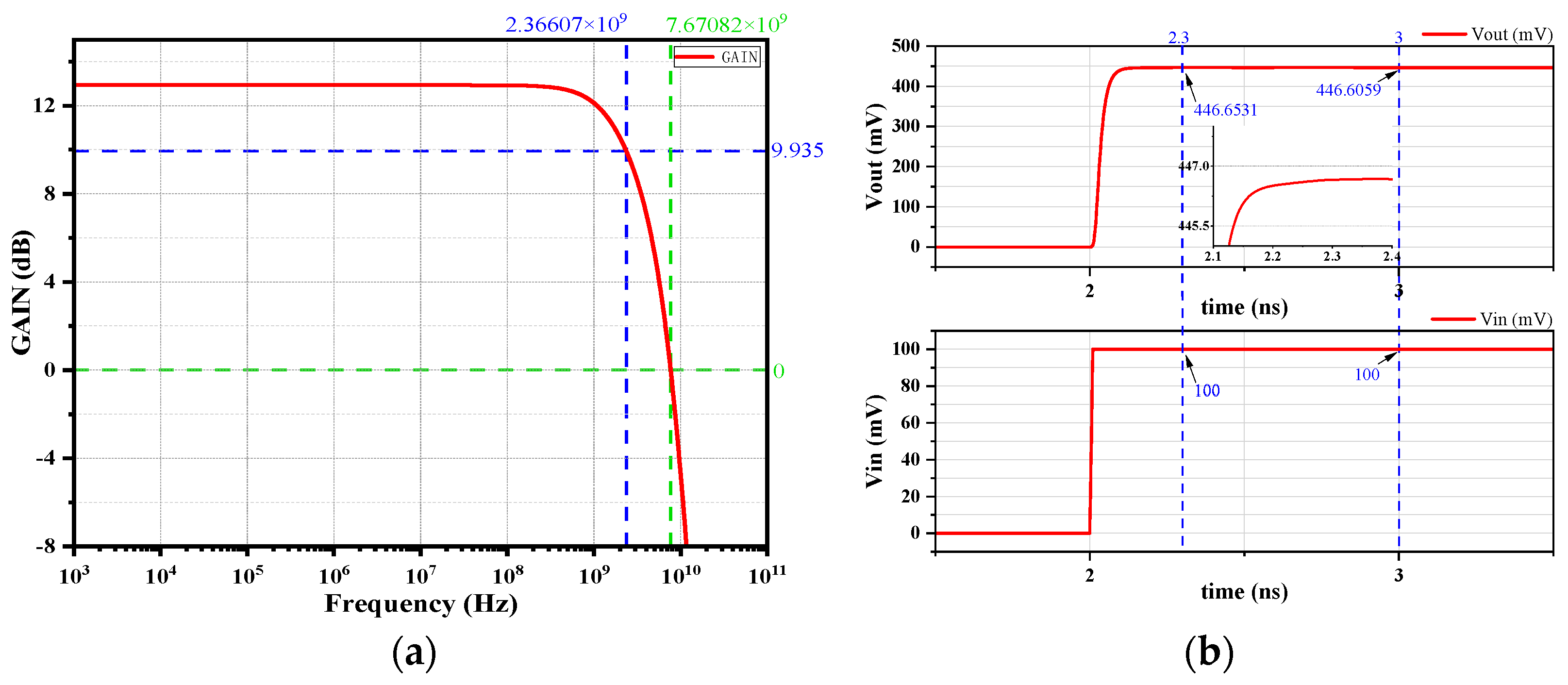
5.1. Simulation Results of the Open-Loop Amplifier

Figure 10 illustrates the relationship of DC gain versus input amplitude of an open-loop amplifier. Figure 10a shows that the open-loop amplifier maintains good DC gain flatness under both TT and SF process corners. The DC gain flatness decreases under SS and FF process corners, while the FS process corner exhibits poor DC gain flatness performance, which is therefore not presented in the figure. The carrier mobility of PMOS deviates more significantly compared to NMOS under slow corner conditions, resulting in substantial DC operating point drift in the amplifier despite the implementation of common-mode feedback. This operating point drift becomes particularly pronounced when the carrier mobilities of NMOS and PMOS change in opposite directions. Figure 10b further indicates that the dynamic error of SFDR also worsens under the SS corner due to relatively poor gain flatness.
To further illustrate the impact of process variations and device mismatches on SFDR performance, Figure 11 presents approximately 250 Monte Carlo simulation results under a 900 MHz input signal scenario. The results demonstrate that the output SFDR of the MDAC is higher than 50 dB.
When the input differential amplitude is 100 mV and the initial gain is 4.466, the output VPP should be 893.2 mV. The normalized maximum gain deviation is 0.001138 under the TT corner, which meets the 9-bit accuracy requirement. If reducing the input amplitude to improve accuracy, when the input differential amplitude is 95 mV and the initial gain is 4.466, then the output VPP should be 848.54 mV. The normalized maximum gain deviation is 0.000078, which meets the 13-bit accuracy requirement.
In terms of dynamic error, since the open-loop amplifier adopts a fully open-loop structure, the dominant pole of the circuit is determined by both the load and output resistance of the amplifier. The dominant pole can be figured out by analyzing Figure 6, which is expressed as:
ω p 1 = 1 R o u t C L = 1   +   g m 27 r o 27 1   +   g m 29 r o 29 1   +   g m 29 r o 29 r o 27 + r o 29 C L
Figure 12a shows the AC response of the harmonic-compensated open-loop amplifier, and it can be observed that the −3 dB bandwidth is approximately 2.366 GHz, with a GBW of 7.67 GHz. In order to more intuitively reflect the impact of bandwidth on dynamic errors, the simulation result of transient response is shown in Figure 12b. The input signal is a step wave with a differential amplitude of 100 mV, and the load is set to 120 fF. From the step response waveform, it can be seen that the input signal undergoes a jump at 2 ns, and the output signal can complete the settling and meet the 10-bit accuracy requirement of dynamic error within approximately 250 ps.

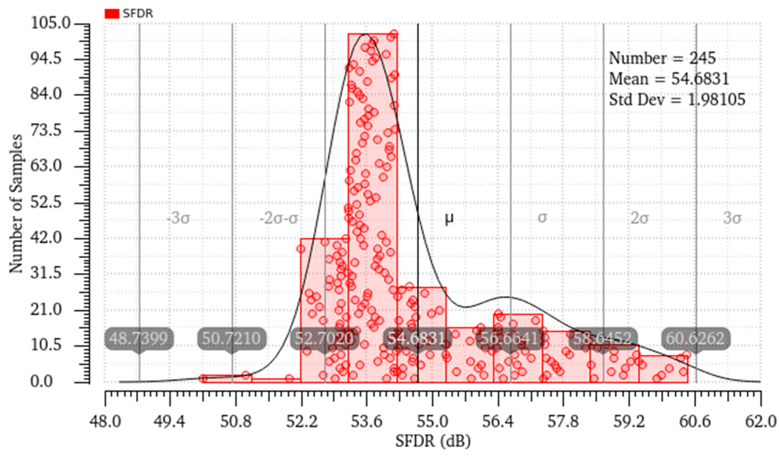
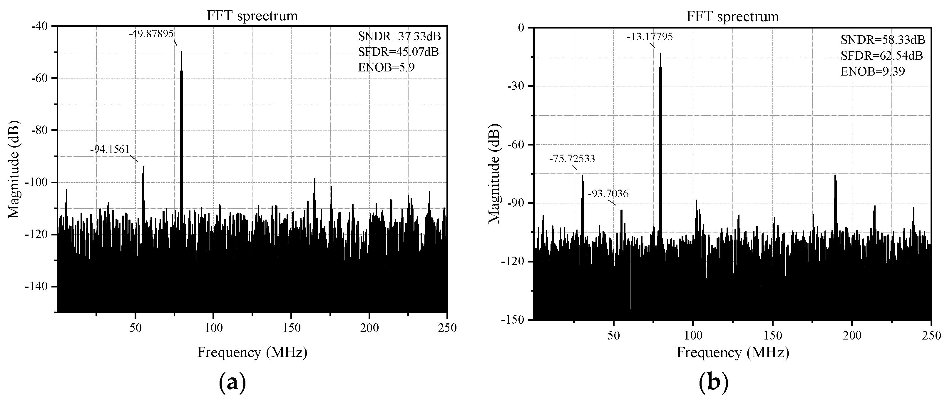
5.2. Simulation Results of the Memory Effect Compensation Circuit

To verify the effectiveness of the memory effect compensation circuit, this work simulates the output spectrum of the double-sampling amplification mode under two conditions: with and without the memory effect compensation circuit. The comparison results of the spectrum are shown in Figure 13. In the simulation, an 80 MHz sine wave is applied to channel 1, and a 55 MHz sine wave is applied to channel 2, both having differential amplitudes of 90 mV, while the output of sub-DAC is manually set to zero. The simulation comparison results show that without the memory effect compensation, the SNDR is compressed to only 37.33 dB because of channel crosstalk. However, when the memory effect compensation circuit is active, the crosstalk signal is canceled before amplification, resulting in an output SNDR of 58.33 dB, which is an improvement of 21 dB compared to the previous case.

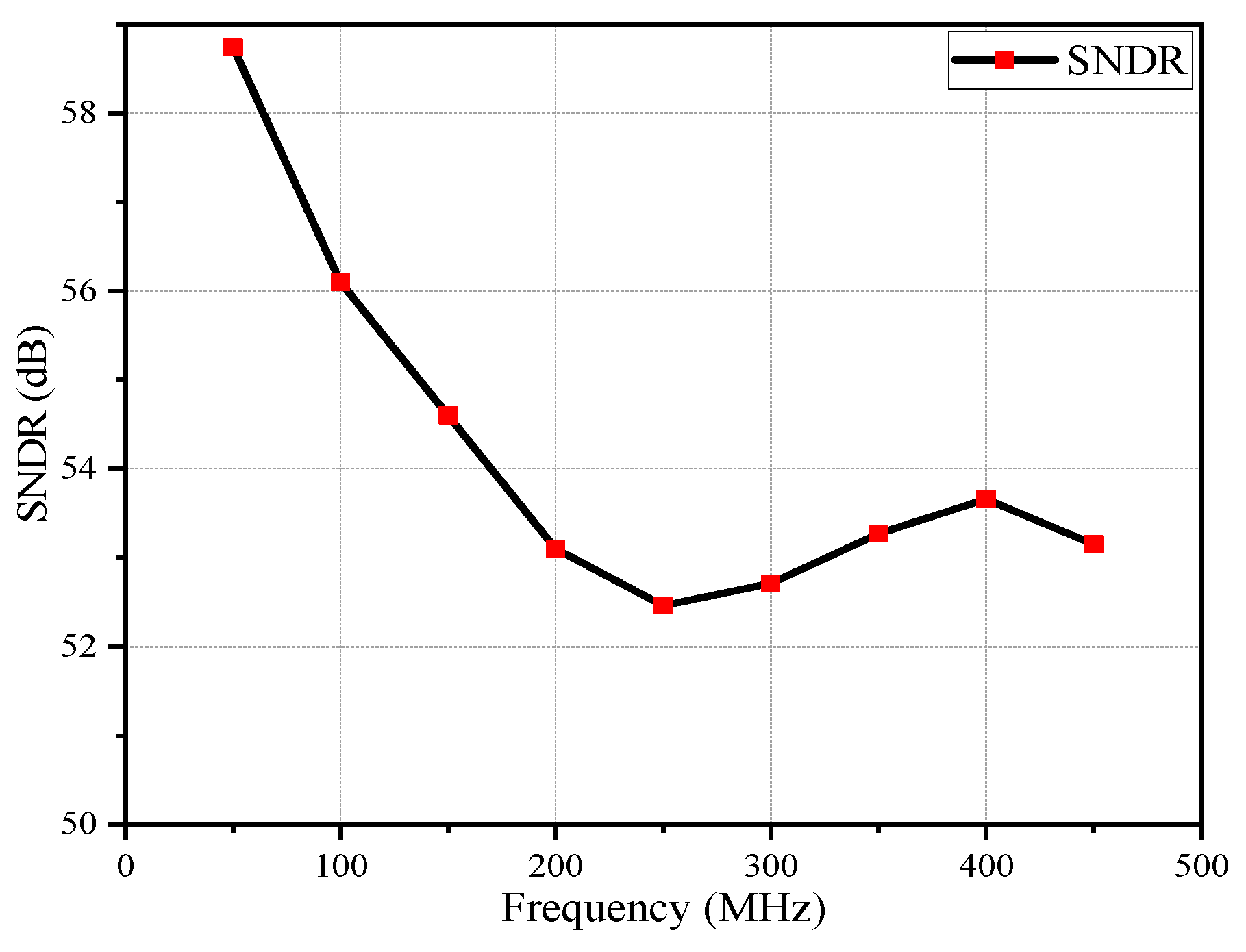
5.3. Simulation Results Comparison

Figure 14 illustrates the relationship between the output SNDR of the pipelined stage and the input signal frequency at an equivalent sampling rate of 1.8 GS/s. The figure shows that the proposed open-loop MDAC provides an output SNDR of at least 50 dB under the double-sampling mode, equivalent to an 8-bit ENOB settling precision, which can satisfy the design requirements for the first stage of a 10-bit ENOB pipelined ADC. Table 1 shows a comparison between the state-of-the-art pipelined ADC [8,11,14,18,19,20,21,22,23,24,25,26,27] and this work.

6. Conclusions

This paper proposes a prototype open-loop pipelined ADC stage. An innovative linearization technique based on the current-mode compensation circuit is employed for the MDAC. The current-mode compensation circuit can provide positive third-order harmonics related to the input signal to counteract the negative third-order harmonics derived from the gain compression of the preceding amplifier. In addition, the memory effect cancellation technique can alleviate the severe inter-channel crosstalk of the open-loop MDAC in the double-sampling mode. This scheme is optimized by tuning the timing of compensation and aligning the input capacitance of the amplifier, achieving a 21 dB improvement on the output SNDR of the MDAC. The open-loop pipelined ADC stage obtains the least output SNDR of 52.46 dB at 1.8 GS/s while consuming 11.24 mW. The prototype pipelined stage is proven to be sufficient to support the design requirements for a 10-bit pipelined ADC.

Author Contributions

Conceptualization, J.W.; Data curation, J.W.; Formal analysis, J.W.; Investigation, J.W.; Methodology, J.W.; Project administration, Q.M.; Resources, Q.M.; Supervision, Q.M.; Validation, J.W.; Visualization, J.W.; Writing—original draft, J.W.; Writing—review and editing, J.W., S.G., G.L., J.S. and S.L. All authors have read and agreed to the published version of the manuscript.

Funding

This research funded by National Natural Science Foundation of China, NSFC:U2430210 and Jiangsu Province Key Project, BG2024035.

Data Availability Statement

The data presented in this study are available on request from the corresponding author.

Conflicts of Interest

The authors declare that they have no known competing financial interests or personal relationships that could have appeared to influence the work reported in this paper.

References

  1. Liu, M.; Li, D.; Zhu, Z. A Dual-Supply Two-Stage CMOS Op-amp for High-Speed Pipeline ADCs Application. IEEE Trans. Circuits Syst. II Express Briefs 2019, 67, 650–654. [Google Scholar] [CrossRef]
  2. Feng, X.; Ma, S.; Zou, M.; Wu, T. A High Gain and Wide Bandwidth Dual-Power CMOS Op-amp for High-Speed ADCs Application. In Proceedings of the 2023 IEEE 15th International Conference on ASIC (ASICON), Nanjing, China, 24–27 October 2023; pp. 1–4. [Google Scholar] [CrossRef]
  3. Liu, Y.; Shen, Y.; Chen, M.; Xu, H.; Chen, X.; Liu, J.; Wang, Z.; Yu, F. A Single-Stage Gain-Boosted Cascode Amplifier with Three-Layer Cascode Feedback Amplifier for Front-End SHA in High-Linearity Pipelined ADC. IEEE Trans. Very Large Scale Integr. (VLSI) Syst. 2024, 33, 47–51. [Google Scholar] [CrossRef]
  4. Zhang, C.; Wei, J.; Yang, Y.; Liu, M. A 12-bit 1.25 GS/s RF sampling pipelined ADC using a bandwidth-expanded residue amplifier with bias-free gain-boost technique. Microelectron. J. 2022, 130, 105611. [Google Scholar] [CrossRef]
  5. Lagos, J.; Hershberg, B.; Martens, E.; Wambacq, P.; Craninckx, J. A Single-Channel, 600-MS/s, 12-b, Ringamp-Based Pipelined ADC in 28-nm CMOS. IEEE J. Solid-State Circuits 2019, 54, 403–416. [Google Scholar] [CrossRef]
  6. Lagos, J.; Hershberg, B.; Martens, E.; Wambacq, P.; Craninckx, J. A 1Gsps, 12-bit, single-channel pipelined ADC with dead-zone-degenerated ring amplifiers. In Proceedings of the 2018 IEEE Custom Integrated Circuits Conference (CICC), San Diego, CA, USA, 8–11 April 2018; pp. 1–4. [Google Scholar]
  7. Zhang, H.; He, B.; Guo, X.; Wu, D.; Liu, X. A 1-GS/s 12-bit Single-Channel Pipelined ADC in 28-nm CMOS with Input-Split Fully Differential Ring Amplifier. IEEE Trans. Very Large Scale Integr. (VLSI) Syst. 2023, 31, 1931–1938. [Google Scholar] [CrossRef]
  8. Jiang, W.; Zhu, Y.; Zhang, M.; Chan, C.-H.; Martins, R.P. A Temperature-Stabilized Single-Channel 1-GS/s 60-dB SNDR SAR-Assisted Pipelined ADC with Dynamic Gm-R-Based Amplifier. IEEE J. Solid-State Circuits 2019, 55, 322–332. [Google Scholar] [CrossRef]
  9. Park, Y.; Song, J.; Choi, Y.; Lim, C.; Ahn, S.; Kim, C. An 11-b 100-MS/s Fully Dynamic Pipelined ADC Using a High-Linearity Dynamic Amplifier. IEEE J. Solid-State Circuits 2020, 55, 2468–2477. [Google Scholar] [CrossRef]
  10. Kim, Y.-H.; Cho, S. A 1-GS/s 9-bit Zero-Crossing-Based Pipeline ADC Using a Resistor as a Current Source. IEEE Trans. Very Large Scale Integr. (VLSI) Syst. 2016, 24, 2570–2579. [Google Scholar] [CrossRef]
  11. Yu, L.; Miyahara, M.; Matsuzawa, A. A 9-bit 1.8 GS/s 44 mW Pipelined ADC Using Linearized Open-Loop Amplifiers. IEEE J. Solid-State Circuits 2016, 51, 2210–2221. [Google Scholar] [CrossRef]
  12. Park, C.; Chen, T.; Noh, K.; Zhou, D.; Prakash, S.; Alizadeh, M.N.; Karsilayan, A.I.; Chen, D.; Geiger, R.L.; Silva-Martinez, J. A 12-Bit 125-MS/s 2.5-Bit/Cycle SAR-Based Pipeline ADC Employing a Self-Biased Gain Boosting Amplifier. IEEE Trans. Circuits Syst. I Regul. Pap. 2020, 67, 3618–3629. [Google Scholar] [CrossRef]
  13. Dias, D.; Goes, J.; Costa, T. A PVT-Robust Open-loop Gm-Ratio ×16 Gain Residue Amplifier for >1 GS/s Pipelined ADCs. In Proceedings of the 2024 IEEE International Symposium on Circuits and Systems (ISCAS), Singapore, 19–22 May 2024; pp. 1–5. [Google Scholar] [CrossRef]
  14. Wu, C.; Yuan, J. A 12-Bit, 300-MS/s Single-Channel Pipelined-SAR ADC with an Open-Loop MDAC. IEEE J. Solid-State Circuits 2019, 54, 1446–1454. [Google Scholar] [CrossRef]
  15. Sehgal, R.; Van Der Goes, F.; Bult, K. A 13-mW 64-dB SNDR 280-MS/s Pipelined ADC Using Linearized Integrating Amplifiers. IEEE J. Solid-State Circuits 2018, 53, 1878–1888. [Google Scholar] [CrossRef]
  16. Bult, K.; Wallinga, H. A class of analog CMOS circuits based on the square-law characteristic of an MOS transistor in saturation. IEEE J. Solid-State Circuits 1987, 22, 357–365. [Google Scholar] [CrossRef]
  17. Borkar, B.D.; Tijare, A.D. VLSI implementation of current mode analog multiplier. In Proceedings of the 2015 International Conference on Communications and Signal Processing (ICCSP), Melmaruvathur, India, 2–4 April 2015; pp. 0531–0534. [Google Scholar] [CrossRef]
  18. Naderi, A.; Mojarrad, H.; Ghasemzadeh, H.; Khoei, A.; Hadidi, K. Four-quadrant CMOS analog multiplier based on new current squarer circuit with high-speed. In Proceedings of the IEEE EUROCON 2009, St. Petersburg, Russia, 18–23 May 2009; pp. 282–287. [Google Scholar] [CrossRef]
  19. Zhong, L.; Cheng, H.; Deng, H. A double sampling S/H circuit for dual-channel pipelined ADC based on op-sharing. In Proceedings of the 2013 International Conference on Anti-Counterfeiting, Security and Identification (ASID), Shanghai, China, 25–27 October 2013; pp. 1–5. [Google Scholar] [CrossRef]
  20. Kim, H.-J.; An, T.-J.; Myung, S.-M.; Lee, S.-H. Time-Interleaved and Circuit-Shared Dual-Channel 10 b 200 MS/s 0.18 μm CMOS Analog-to-Digital Convertor. IEEE Trans. Very Large Scale Integr. (VLSI) Syst. 2013, 21, 2206–2213. [Google Scholar] [CrossRef]
  21. Xia, B.; Valdes-Garcia, A.; Sanchez-Sinencio, E. A 10-bit 44-MS/s 20-mW Configurable Time-Interleaved Pipeline ADC for a Dual-Mode 802.11b/Bluetooth Receiver. IEEE J. Solid-State Circuits 2006, 41, 530–539. [Google Scholar] [CrossRef]
  22. Devarajan, S.; Singer, L.; Kelly, D.; Pan, T.; Silva, J.; Brunsilius, J.; Rey-Losada, D.; Murden, F.; Speir, C.; Bray, J.; et al. A 12-b 10-GS/s Interleaved Pipeline ADC in 28-nm CMOS Technology. IEEE J. Solid-State Circuits 2017, 52, 3204–3218. [Google Scholar] [CrossRef]
  23. Sehgal, R.; van der Goes, F.; Bult, K. A 12 b 53 mW 195 MS/s Pipeline ADC with 82 dB SFDR Using Split-ADC Calibration. IEEE J. Solid-State Circuits 2015, 50, 1592–1603. [Google Scholar] [CrossRef]
  24. Wang, X.; Shi, M.; Li, P.; Liu, J.; Huang, Z.; Chen, C.; Jiang, W. A 10b 1. In 25GS/s Residue Post-Amplified Pipelined-SAR ADC with Supply-and-Temperature Stabilized Open-Loop Residue Amplifier. In Proceedings of the 2023 IEEE International Symposium on Circuits and Systems (ISCAS), Monterey, CA, USA, 21–25 May 2023; pp. 1–5. [Google Scholar] [CrossRef]
  25. Yu, Q.; Pu, J.; Luo, J.; Huang, Z.; Wu, J.; Zhu, X.; Xiang, F.; Chen, L.; Li, J.; Li, Q.; et al. A 12b 8GS/s Time-Interleaved 2b/cycle Pipelined-SAR ADC with Layout-Customized Bootstrap and Super- Source-Follower Based Open-Loop Residue Amplifier. In Proceedings of the 2022 IEEE Asian Solid-State Circuits Conference (A-SSCC), Taipei, Taiwan, 6–9 November 2022; pp. 1–3. [Google Scholar] [CrossRef]
  26. Li, N.; Zhang, H.; Liu, B.; Pei, L.; Wang, J.; Qi, H.; Zhang, J.; Wang, X.; Zhang, H. A 10-Bit 500-MS/s Pipelined SAR ADC with Nonlinearity-Compensated Open-Loop Amplifier and Parallel Conversion Through Comparator Reusing. IEEE Trans. Circuits Syst. II Express Briefs 2024, 72, 354–358. [Google Scholar] [CrossRef]
  27. Fang, L.; Wen, X.; Fu, T.; Gui, P. A 12-Bit 1 GS/s RF Sampling Pipeline-SAR ADC with Harmonic Injecting Cross-Coupled Pair Achieving 7.5 fj/Conv-Step. IEEE Trans. Circuits Syst. I Regul. Pap. 2022, 69, 3225–3236. [Google Scholar] [CrossRef]
Figure 1. Block diagram of the proposed pipelined ADC stage.
Electronics 14 01753 g001
Figure 2. Principle of post-correction.
Electronics 14 01753 g002
Figure 3. Current squaring circuit.
Electronics 14 01753 g003
Figure 4. The second current squaring circuit.
Electronics 14 01753 g004
Figure 5. First-stage amplifier.
Electronics 14 01753 g005
Figure 6. The overall two-stage open-loop amplifier structure.
Electronics 14 01753 g006
Figure 7. A conventional double-sampling circuit.
Electronics 14 01753 g007
Figure 8. The proposed (a) diagram of the pipelined stage; (b) timing sequence; (c) input terminal of amplifier.
Electronics 14 01753 g008
Figure 9. The proposed pipelined stage with open-loop MDAC.
Electronics 14 01753 g009
Figure 10. Simulated result of (a) DC gain vs. input amplitude, and (b) SFDR vs. input frequency.
Electronics 14 01753 g010
Figure 11. Monte Carlo simulation results of output SFDR.
Electronics 14 01753 g011
Figure 12. (a) The AC response and (b) transient response of harmonic-compensated open-loop amplifier.
Electronics 14 01753 g012
Figure 13. The compared spectrum (a) without and (b) with the memory effect compensation circuit.
Electronics 14 01753 g013
Figure 14. Simulated output SNDR versus input frequency at equivalent sampling rate of 1.8 GS/s.
Electronics 14 01753 g014
Table 1. MDAC performance comparison of pipelined ADC stage.
[11][8][14][27]This Work
Process65 nm28 nm65 nm28 nm45 nm
Supply (V)1.211.20.91.2
Input amplitude (mV)800120016001100850
Sampling rate (GS/s)1.810.311.8
Output accuracy of residual amplifier (bit)797118
Power9.92 mW2.5 mW8.12 mW2.37 mW11.24 mW 1
1 Excluding power supply on clock generator and digital circuit biases.
Disclaimer/Publisher’s Note: The statements, opinions and data contained in all publications are solely those of the individual author(s) and contributor(s) and not of MDPI and/or the editor(s). MDPI and/or the editor(s) disclaim responsibility for any injury to people or property resulting from any ideas, methods, instructions or products referred to in the content.

