Article

Wafer-Level Amplitude Equalizer Based on an Integrated Passive Device Process with Two Resonance Points for Wavy In-Band Transmission

1
Beijing Institute of Radio Measurement, Beijing 100854, China
2
Yangtze Delta Region Institute, University of Electronic Science and Technology of China, Huzhou 313001, China
3
School of Information Engineering, Kunming University, Kunming 650214, China
*
Authors to whom correspondence should be addressed.
Electronics 2025, 14(9), 1715; https://doi.org/10.3390/electronics14091715
Submission received: 24 March 2025 / Revised: 14 April 2025 / Accepted: 19 April 2025 / Published: 23 April 2025
(This article belongs to the Section Microelectronics)

Abstract

:
Amplitude equalizers play an important role in microwave transmission systems, and their performance can directly improve the signal transmission quality. Nowadays, the miniaturized equalizer is in good need of a highly integrated radio frequency (RF) front end. In this paper, a wafer-level amplitude equalizer based on an integrated passive device (IPD) process is proposed. Moreover, the equalizer circuit containing two resonance points within the transmission frequency band is also proposed. The amplitude equalizer operates at the center frequency of 3.88 GHz, with two resonance points of 2.9 GHz and 5.2 GHz; the minimum insertion loss is 1.17 dB, the maximum attenuation is 4 dB, and the in-band voltage standing wave ratio (VSWR) is less than 1.6:1. All the measured results are in good agreement with the designed results. The size of the proposed equalizer is 0.8 mm × 0.65 mm × 0.1 mm (0.011λ × 0.008λ × 0.001λ), which shows great potential in the miniaturization application of the RF microsystem. Furthermore, the new equalizer circuit with two resonance points is especially suitable for wavy in-band transmission.

1. Introduction

Due to the dispersion effects of microwave transmission, as well as the inherent characteristics of the active components (i.e., amplifiers and mixers), gain fluctuations inevitably occur within the operating frequency bands, which may have a serious impact on the quality of signal transmission. Therefore, the in-band flatness has become an important parameter for the design of microwave circuit systems [1,2,3]. To improve the in-band flatness, the equalizer was first proposed by F. E. Terman in the 1940s [4]. D. J. Mellor derived the topology prototype for the matched microstrip equalizer in 1977, which led to significant improvements in the performance and size of the equalizers [5]. Subsequently, waveguide and coaxial implemented equalizers, microstrip equalizers, substrate-integrated waveguide (SIW) equalizers, and semi-lumped equalizers were proposed [6,7,8,9,10]. However, with the development of high-precision microwave communication, microwave measurement equipment, bio-medical detection, and other applications, the amplitude equalizer requirements of in-band flatness and miniaturization are becoming increasingly high [11,12,13], and the traditional design methods may not meet the demands.
Nowadays, miniature passive devices are fabricated on rigid or flexible substrates for specific applications [14,15,16]. Among them, passive devices based on the integrated passive device (IPD) process can be fabricated on wafers (such as silicon, GaAs) used in semiconductor processes and can be compatible with the complementary metal oxide semiconductor (CMOS) process for wafer-level production [17,18]. Furthermore, IPD processes have the advantage of high processing line accuracy and consistency compared with processes on ceramics or printed circuit boards (PCBs). RF passive devices such as filters, power dividers, and baluns are designed and fabricated based on the IPD process, which shows great potential for hybrid integration and applications in RF microsystems [19,20,21,22,23]. Moreover, traditional equalizer circuits always have one resonance point and can only adjust the microwave system in-band flatness with a single slope. However, the in-band transmission gain is always wavy, adjustment with a single slope is difficult to meet the requirement, and the cascade of multiple equalizers greatly increases the circuit size [4,24]. Therefore, equalizers with multiple slope adjustment capabilities are needed, which means that the equalizer with multiple resonance points needs to be designed and fabricated.
In this paper, a wafer-level amplitude equalizer based on the IPD process is proposed. First, an equalizer circuit topology with two resonance points is proposed, integrating a bridged-T attenuator circuit and a frequency selection circuit. Then, the wafer-level equalizer is designed and fabricated based on the GaAs-IPD process with a compact size of 0.8 mm × 0.65 mm × 0.1 mm (0.011λ × 0.008λ × 0.001λ). The equalizer operates at the center frequency of 3.88 GHz, with two resonance points of 2.9 GHz and 5.2 GHz; the minimum insertion loss is 1.17 dB, the maximum attenuation is 4 dB, and the in-band voltage standing wave ratio (VSWR) is less than 1.6:1. All the measured results are in good agreement with the designed results. Thus shows great potential in the miniaturization application of RF microsystems. Furthermore, the equalizer with two resonance points is especially suitable for wavy in-band transmission.

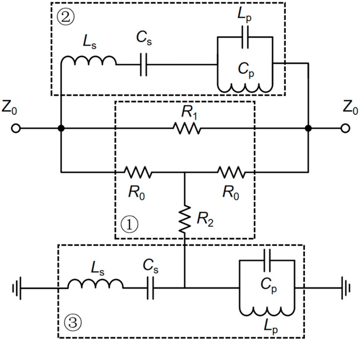
2. Circuit Design and Fabrication Process

The proposed equalizer circuit in this work consists of an attenuator circuit and a frequency selection circuit. The circuit topology of the proposed equalizer is shown in Figure 1. The attenuator circuit determines the maximum attenuation of the equalizer. Among the existing attenuator circuits, the bridged-T attenuator circuit has the advantages of simple structure, good impedance matching, and flexible design [6,10]. The structure of the bridged-T attenuator is shown in unit ① in Figure 1.
The two series resistors R0 are equal to the source/load impedance (Z0) of 50 ohm. And, resistance R1 and R2 can be calculated as follows:
R 1 = Ζ 0 ( 10 A 20 1 )
R 2 = Z 0 ( 1 10 A 20 1 )
where A represents the expected attenuation value of the bridged-T attenuator. The attenuation can be adjusted by changing the value of R1 and R2 [10].
The working band of the equalizer can be determined by the frequency selection circuit. In this paper, unit ② and unit ③ in Figure 1 constitute the frequency selection circuit, and the circuit topology of the equalizer with two resonance points is proposed. As shown in unit ② in Figure 1, two resonance points can be obtained within the band by a series connection of a parallel resonance circuit and a series resonance circuit. In detail, the parallel resonance circuit and the series resonance circuit in unit ② can each produce one resonance point. The resonance point frequency (f) of each resonance circuit can be obtained by the following equation:
f = 1 2 π L C
where L and C represent the inductance and capacitance of the resonance circuit, respectively. The center frequency (f0) of the equalizer can be obtained by the equation shown as follows:
f 0 = f s f p
where fs and fp represent the resonance point frequency of the series resonance circuit and parallel resonance circuit. Furthermore, the unit ③ circuit is added to improve the impedance matching of the equalizer and constitutes the selection circuit with unit ②.
The IPD process has the advantage of compatibility with the semiconductor processes. The GaAs semiconductor process, as a mainstream semiconductor process, is widely used in the manufacture of RF amplifiers and mixers and has the characteristics of low cost and simple processing. Therefore, this work selects the IPD process based on the GaAs wafer and tapes out the chips to the GaAs process foundry. Figure 2 shows the multi-layer structures of the IPD process on the GaAs wafer. A series of layers such as gold layers (i.e., M0, M1, and M2), Si3N4 layers (i.e., N1, N2, N3, and VM), and polyimide layers (i.e., PV) can be fabricated and used for forming a MIM (metal–insulator–metal) capacitor, a high-Q value spiral inductor, and a thin-film resistor; then, the circuit shown in Figure 2a can be constructed. The function and thickness of layers, the structural relationship between the layers, and the process steps are similar to the descriptions mentioned in the previous work [19]. The back gold layer (M0) with a thickness of 2 μm is electroplated on the bottom surface of the GaAs wafer, which is used as the equivalent ground of the device. The SiN adhesion layer (N1) with a thickness of 0.16 μm is grown on the surface of the GaAs wafer. And, the TaN thin-film resistor layer is deposited by sputtering deposition. Next, the first metal layer (M1) is patterned and grown with a thickness of 1 μm, which is used for the inductor connecting line and the lower electrode plate of the MIM capacitor. The SiN dielectric layer (N2) with a thickness of 0.4 μm is grown, and the second metal (M2) is electroplated with a thickness of 4 μm, which is used for the planar spiral inductor and the upper electrode plate of the MIM capacitor. Next, the third SiN passivation layer (N3) with a thickness of 5 μm is grown, which aims to protect the circuit. After the circuit structure was completed on the GaAs wafer, the wafer was divided into multiple independent chips by dicing process.

3. Results and Discussion

In this work, the required maximum attenuation of the amplitude equalizer is 4 dB, and the equalizer operates at the center frequency of 3.88 GHz, with two resonance points of 2.9 GHz and 5.2 GHz. According to Equations (1) and (2), the resistance R1 and R2 can be obtained as shown in Table 1. Based on the derivation of Equations (3) and (4), the chip size of IPD circuit models (i.e., inductor and capacitor) and simple design are also considered, the component values are set as the same value in units ② and ③, and the models of inductors and capacitors are selected as the value in Table 1.
Based on the IPD process, the electromagnetic field model of the equalizer is designed with FEM software HFSS (Ansys Electronics Desktop 2020 R2). The layout of the inductor, capacitor, resistor, and ground–signal–ground (GSG) pads are marked in Figure 3a. Figure 3b shows the fabricated equalizer, and its physical size is only 0.8 mm × 0.65 mm × 0.1 mm. Then, the equalizer is measured using a vector network analyzer (Keysight N5247A, Santa Rosa, CA, USA) with on-wafer GSG probes (Cascade ACP), as shown in Figure 4.
The measured results of S-parameters are shown in Figure 5a with a solid line and show that the maximum attenuation of the amplitude equalizer is ~4 dB; the equalizer operates at the center frequency of 3.88 GHz, with two resonance points of ~2.9 GHz and ~5.2 GHz. The minimum insertion loss is 1.17 dB, and the in-band return loss is greater than 15 dB. Moreover, the VSWR is less than 1.6:1, as shown in Figure 5b, which means that the equalizer has good matching with source/load impedance. The simulated results are shown with a dashed line. In summary, all the measured results are in good agreement with the designed results, and slight deviation is mainly due to the error brought by the test environment. Therefore, the feasibility of the proposed circuit and the accuracy of the IPD process design method are verified.
Table 2 shows a list of concerned performance parameters of various amplitude equalizers. In reference [6], the equalizer is integrated on a system-on-chip (SOC) chip fabricated by the SiGe BiCMOS process, which also has a compact size of the equalizer by the IPD process. However, the equalizer based on the IPD process has the capability of miniaturization and monolithic integration. This means that the IPD equalizer has better integration flexibility, which is more suitable for hybrid integration and application in RF microsystems. The amplitude equalizers designed by coplanar waveguide and SIW methods and fabricated on Al2O3 ceramic are presented in [7,8], which have the capability of monolithic integration and larger layout size. Although the equalizer designed by the dual-mode SIW method also has two resonance points, it increases the difficulty of design and device size compared with the method proposed in this work. The equalizer in [9] is designed by the semi-lumped microstrip method and fabricated by the PCB process on a microwave board, which has a great improvement when compared to the equalizers designed with the distributed microstrip method. However, it is still larger in size compared to the equalizer proposed in this work. Compared to the equalizer in [10], the proposed equalizer is monolithic and improves the circuit topology with two resonance points, which means better adjustment capability. In summary, the proposed amplitude equalizer in this paper has obvious advantages in circuit topology, layout size, integration flexibility, and adjustment capability.

4. Conclusions

This paper proposed a wafer-level amplitude equalizer based on the GaAs-IPD process. A circuit topology of the equalizer with two resonance points is also proposed. The wafer-level amplitude equalizer with two resonance points is designed and fabricated based on the IPD process. The measured results show good agreement with the design parameters. Wafer-level amplitude equalizers with compact size show great potential in the miniaturization application of the RF microsystem. Furthermore, the equalizing effect with two resonance points may have good applications in the adjustment of wavy in-band transmission of microwave systems. However, only two resonance points can be obtained by the proposed circuit topology, including the series connection of a parallel resonance circuit and a series resonance circuit in frequency selection circuit, and circuit topologies of equalizers with multiple resonance points need to be studied in the future.

Author Contributions

Conceptualization, M.X., X.Y., and Y.L.; formal analysis, G.L.; investigation, X.Y.; methodology, M.X. and X.L.; software, X.Y. and G.L.; writing—original draft, X.Y.; writing—review and editing, X.S. and W.L. All authors have read and agreed to the published version of the manuscript.

Funding

This research was funded by the National Natural Science Foundation of China, grant number 61864004, and the Natural Science Foundation of Fujian Province, grant numbers 2023J011802 and 2023J05301.

Data Availability Statement

The data that support the findings of this study are available from the corresponding authors upon reasonable request.

Conflicts of Interest

The authors declare no conflicts of interest.

References

  1. Sheikholeslami, A. Equalizer circuit [Circuit Intuitions]. IEEE Solid-State Circuits Mag. 2020, 12, 6–7. [Google Scholar] [CrossRef]
  2. Li, Q.; Yang, T. Dispersion analysis of shielded asymmetrical coplanar stripline and its broadband transition to microstrip. In Proceedings of the IEEE MTT-S International Wireless Symposium, Shanghai, China, 20–23 September 2020; pp. 1–3. [Google Scholar]
  3. Jain, N.; Brown, B. Dispersion characteristics of microstrip transmission line on glass microwave IC’s. IEEE Microw. Guid. Wave Lett. 1997, 7, 344–346. [Google Scholar] [CrossRef]
  4. Terman, F.E. Network theory, filters, and equalizers. Proc. IRE 1943, 31, 288–302. [Google Scholar] [CrossRef]
  5. Mellor, D.J. On the design of matched equalizers of prescribed gain versus frequency profiles. In Proceedings of the IEEE MTT-S International Microwave Symposium Digest, San Diego, CA, USA, 21–23 June 1977; pp. 308–311. [Google Scholar]
  6. Lakshminarayanan, S.; Hofmann, K. A digitally controllable passive variable slope gain equalizer for wideband radio frequency system-on-chip applications. In Proceedings of the 32nd IEEE International System-on-Chip Conference, Singapore, 3–6 September 2019; pp. 461–465. [Google Scholar]
  7. Pang, X.; Xia, L.; Jiao, J. A gain equalizer based on grounded coplanar waveguide with sprial-shaped defected ground. In Proceedings of the IEEE 9th International Symposium on Microwave, Antenna, Propagation and EMC Technologies for Wireless Communications, Chengdu, China, 26–29 August 2022; pp. 15–19. [Google Scholar]
  8. Zhang, D.; Liu, Q.; Zhou, D.; Wang, S.; Zhang, Y. A gain equalizer based on dual-mode circular substrate integrated waveguide resonators. IEEE Microw. Wirel. Compon. Lett. 2017, 27, 539–541. [Google Scholar] [CrossRef]
  9. Xiao, X.; Li, W. A novel design and realization of microstrip lumped-like amplitude equalizer. In Proceedings of the IEEE International Conference on Microwave and Millimeter Wave Technology, Beijing, China, 5–8 June 2016; pp. 293–295. [Google Scholar]
  10. Li, S.; Ma, L.; Wang, L.; Wu, B.; Cheng, Y.; Lei, X.; Liu, F.; Cheng, G.J. An ultrawideband GaAs mmic microstrip directional coupler with high directivity and very flat coupling. IEEE Trans. Microw. Theory Tech. 2022, 70, 2271–2279. [Google Scholar] [CrossRef]
  11. Zhang, Y.; Xu, J.; He, C. A directivity-compensated wideband microstrip coupler based on capacitive-loading patches and reflectionless amplitude equalizers. IEEE Microw. Wirel. Compon. Lett. 2025, 35, 189–192. [Google Scholar] [CrossRef]
  12. Scheder, A.; Pfahler, T.; Bridier, A.; Vossiek, M. An ultra-wideband microstrip gain equalizer on thin-film ceramic for future millimeter wave applications up to and beyond 120 GHz. In Proceedings of the IEEE Wireless and Microwave Technology Conference, Clearwater, FL, USA, 15–16 April 2024; pp. 1–4. [Google Scholar]
  13. Han, L. A reconfigurable microwave equalizer with different maximum attenuations based on RF MEMS switches. IEEE Sens. J. 2016, 16, 17–18. [Google Scholar] [CrossRef]
  14. Wu, Y.; Yeng, I.; Yu, H. The improvement of CoZrTaB thin films on different substrates for flexible device applications. AIP Adv. 2021, 11, 025139. [Google Scholar] [CrossRef]
  15. Wu, Y.; Yu, H. A low-cost novel method to fabricate integrated magnetic core inductor embedded in organic substrate. IEEE Trans. Magn. 2022, 58, 1–5. [Google Scholar] [CrossRef]
  16. Xu, W.; Sinha, S.; Dastagir, T.; Wu, H.; Bakkaloglu, B.; Gardner, D.; Cao, Y.; Yu, H. Performance enhancement of on-chip inductors with permalloy magnetic rings. IEEE Electron Device Lett. 2010, 32, 69–71. [Google Scholar] [CrossRef]
  17. Li, K.; Wu, Y.; Lai, Z.; Yang, Q.; Wang, W. An Iterative extremely accurate generalized design methodology for TSV-based hybrid AlScN FBAR and IPD filtering chips. IEEE Trans. Microw. Theory Tech. 2025, 1–12. [Google Scholar] [CrossRef]
  18. Wei, Y.C.; Wang, C.; Gao, J.Y.; Meng, F.Y.; Wang, X.L.; Wu, Y.L. Lumped dual-band transformer with chebyshev and quasi-elliptic responses based on GaAs-IPD. IEEE Trans. Compon. Packag. Manuf. Technol. 2025, 15, 339–346. [Google Scholar] [CrossRef]
  19. Li, X.; Xing, M.; Liu, G.; Yang, X.; Dai, C.; Hou, M. Compact, reflectionless band-pass filter: Based on GaAs IPD process for highly reliable communication. Electronics 2021, 10, 2998. [Google Scholar] [CrossRef]
  20. Chu, H.N.; Jiang, M.J.; Ma, T.G. On-chip dual-band millimeter-wave power divider using GaAs-based IPD process. IEEE Microw. Wirel. Compon. Lett. 2020, 30, 173–176. [Google Scholar] [CrossRef]
  21. Zoschke, K.; Wolf, M.J.; Topper, M.; Ehrmann, O.; Fritzsch, T.; Kaletta, K. Fabrication of application specific integrated passive devices using wafer level packaging technologies. IEEE Trans. Adv. Packag. 2007, 30, 359–368. [Google Scholar] [CrossRef]
  22. Li, C.C.; Hou, F.; Cao, Y.L.; Chen, W.; Liu, Q.; Qiu, L.F. Silicon-based 3-D self-packaged filtering power divider based on a multimode resonator. IEEE Microw. Wirel. Compon. Lett. 2025, 1–4. [Google Scholar] [CrossRef]
  23. Yang, X.; Sun, X.; Lu, Y. Silicon bridge for high-level RF microsystem package and mixed signals transmission. In Proceedings of the IEEE MTT-S International Microwave Workshop Series on Advanced Materials and Processes for RF and THz Applications, Chengdu, China, 13–15 November 2023; pp. 1–2. [Google Scholar]
  24. Zhang, A.; Xu, J.; Liu, Z. A microstrip linear-phase BPF using dual-band negative group delay equalizers. IEEE Microw. Wirel. Compon. Lett. 2024, 34, 387–390. [Google Scholar] [CrossRef]
Figure 1. The circuit topology of the proposed equalizer. ① Circuit structure of the bridged-T attenuator. ② ③ Circuit structure of the frequency selection circuit.
Electronics 14 01715 g001
Figure 2. Structure schematic and major fabrication steps of the GaAs IPD process. (a) Structure schematic (cross-section) of the GaAs IPD process. (b) Steps of the GaAs IPD process. I. GaAs substrate with the M0 layer (Au). II. The N1 layer (Si3N4) is deposited on the GaAs substrate. III. The VM layer (Si3N4 passivation) is deposited. IV. TaN is deposited for the thin-film resistor. V. The M1 layer (Au) is deposited. VI. The N2 layer (Si3N4) is deposited as a dielectric layer. VII. The PV layer (polyimide) is deposited between the M1 layer and the M2 layer. VIII. The M2 layer (Au) is deposited.
Electronics 14 01715 g002
Figure 3. Images of the designed and fabricated amplitude equalizer based on the GaAs IPD process. (a) Plane structure of the electromagnetic field model of the proposed amplitude equalizer. (b) Microscope image of the fabricated amplitude equalizer.
Electronics 14 01715 g003
Figure 4. Test environment of the amplitude equalizer. The network analyzer and probe station with GSG probes are marked.
Electronics 14 01715 g004
Figure 5. Simulated and measured results of the proposed amplitude equalizer. (a) S-parameter. (b) VSWR.
Electronics 14 01715 g005
Table 1. Components’ values of the proposed amplitude equalizer.
ComponentValueComponentValue
Ls2.654 nHCs0.597 pF
Lp0.663 nHCp2.389 pF
R050.0 ΩR285.6 Ω
R129.2 Ω
Table 2. Performance summary of the proposed amplitude equalizers.
ReferenceProcessDesign
Method
Wafer
-Level
Integration
Form
Return Loss
(dB)
Resonance
Point
Size
(mm2)
Operating
Frequency
(GHz)
[6]SiGe
BiCMOS
Microstrip
lumped
YesOn chip≤−10One0.4290.2–1.85
[7]Al2O3
ceramic
Coplanar
waveguide
NoMonolithic≤−11One30.46–9
[8]Al2O3
ceramic
Dual-mode SIWNoMonolithic/Two186.213–13.5
[9]PCBMicrostrip
Semi-lumped
NoMonolithic/One5252–3
[10]GaAs IPDMicrostrip
lumped
YesOn chip≤−20One/2–20
This workGaAs IPDMicrostrip
lumped
YesMonolithic≤−15Two0.521–7
Disclaimer/Publisher’s Note: The statements, opinions and data contained in all publications are solely those of the individual author(s) and contributor(s) and not of MDPI and/or the editor(s). MDPI and/or the editor(s) disclaim responsibility for any injury to people or property resulting from any ideas, methods, instructions or products referred to in the content.

