
A Novel Modified Delta-Connected CHB Multilevel Inverter with Improved Line–Line Voltage Levels


Abstract
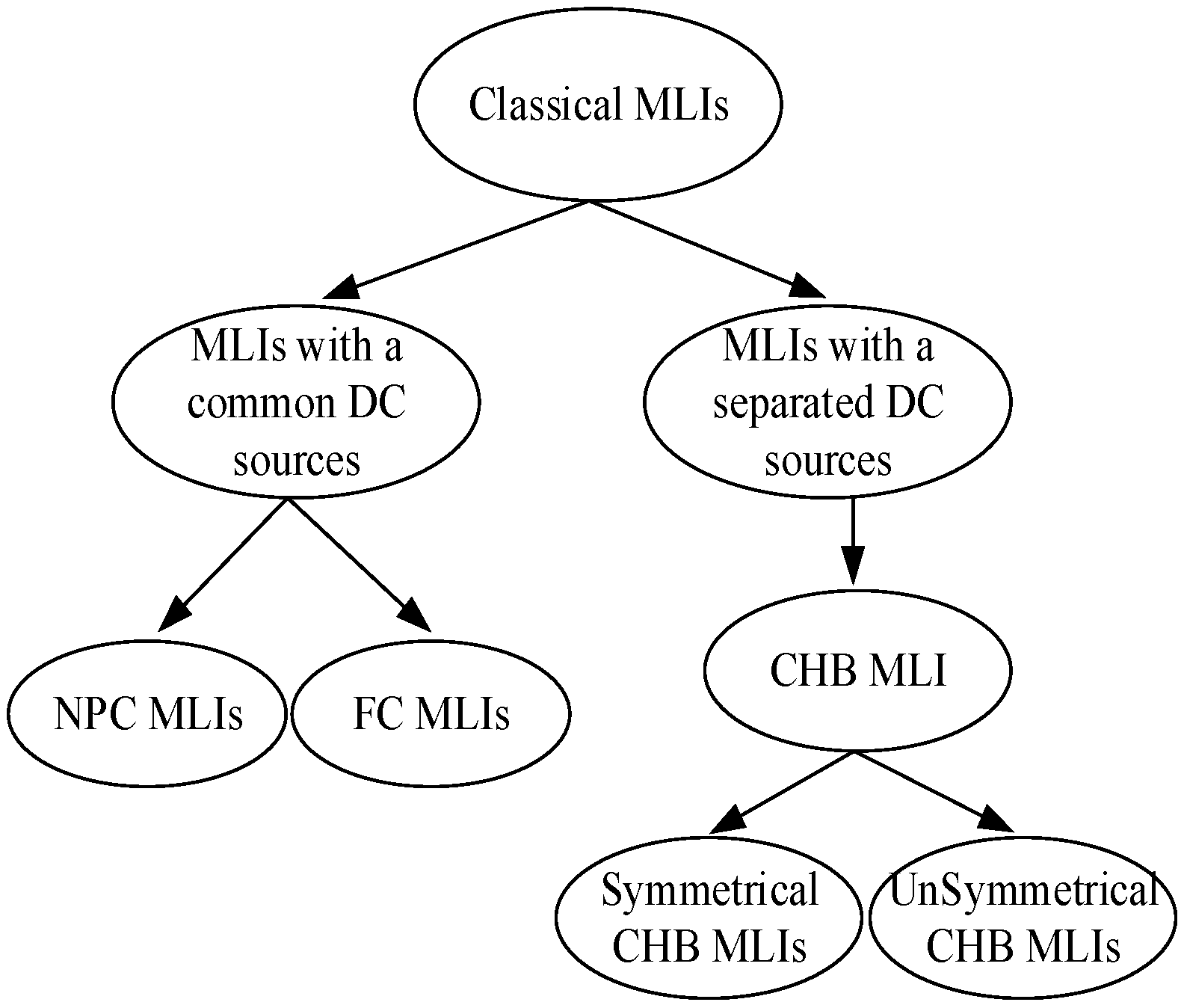
1. Introduction
- The CHB MLI topology has the fewest components among the alternative topologies to produce the same voltage levels.
- Extreme modularity.
- Low cost.
- High inverter efficiency.
- Easy to construct and control.
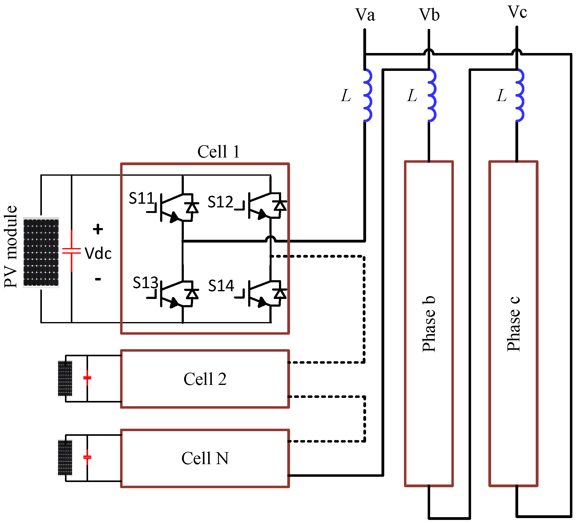
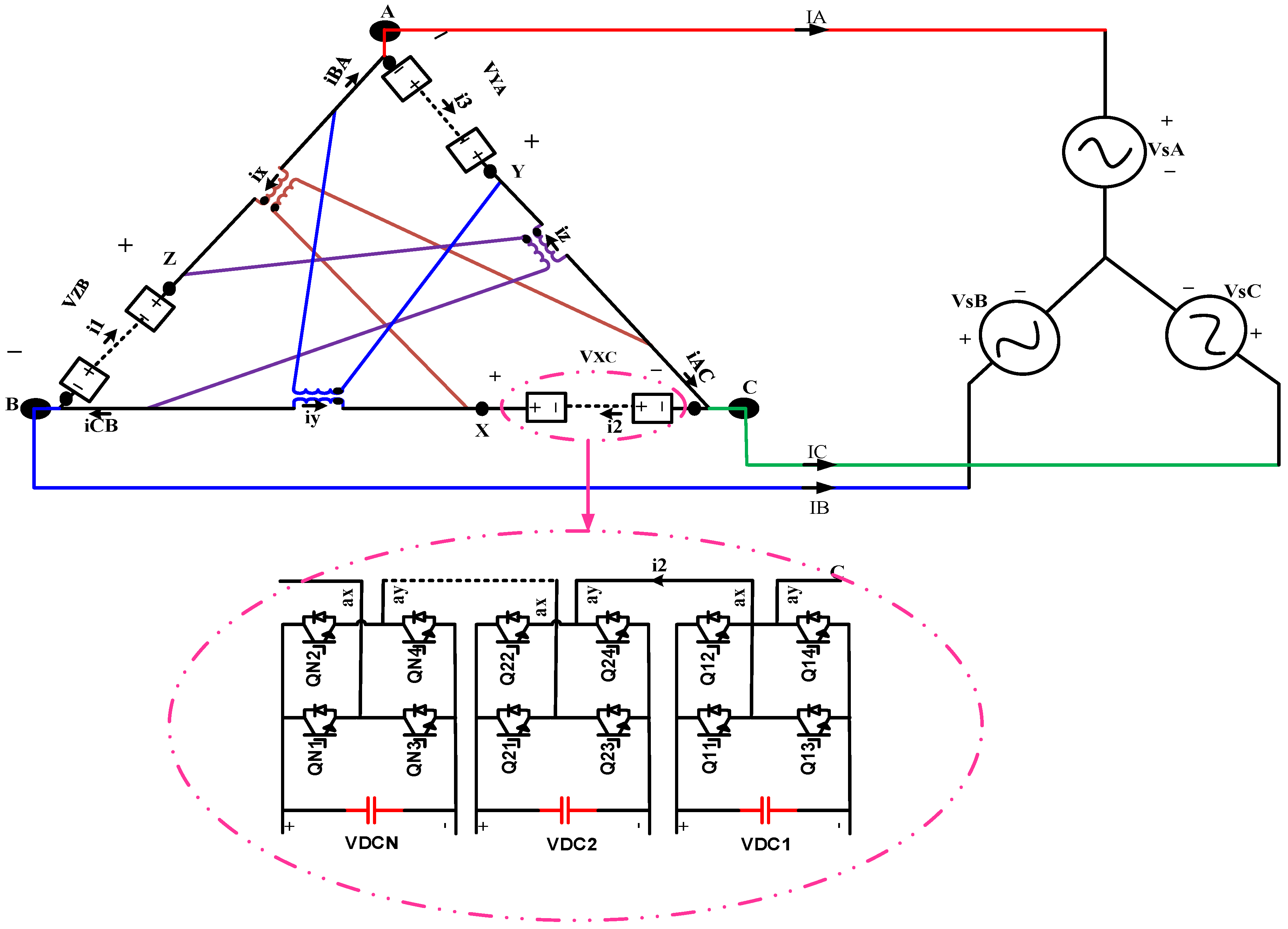
2. Description of the Proposed Topology
- Achieving more voltage levels with fewer switches than the traditional delta-connected multilevel inverter topology.
- Enhanced voltage quality and current waveform.
- Reduced voltage stress on switches compared to the conventional delta-connected CHB configurations.
- ✓
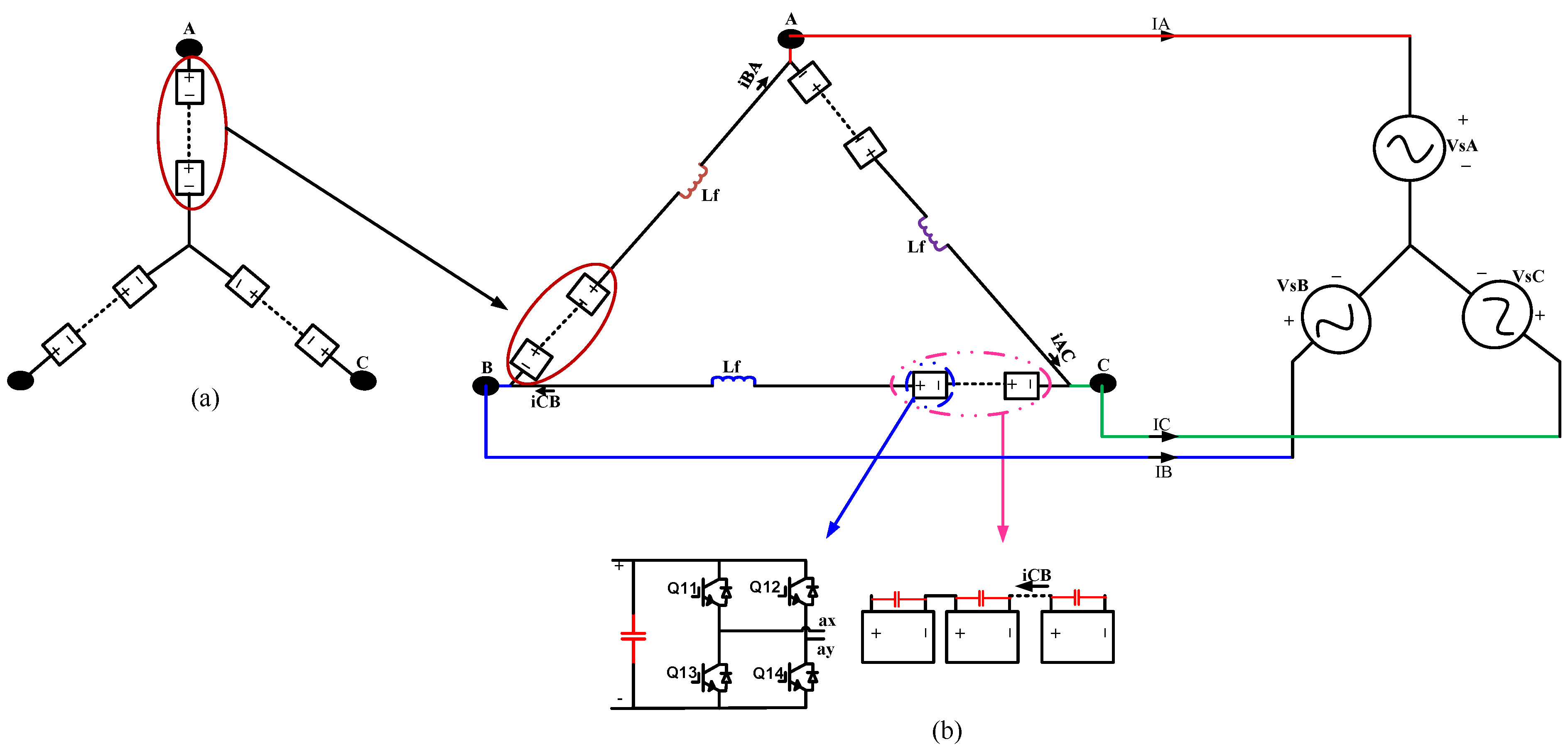
- Stresses on the switches are as follows:where V is the root mean square (RMS) of the line–line grid voltage and N is the number of cascaded H-bridge cells in each phase.
- ✓
- On the other hand, voltage stresses on the switches of the conventional delta-connected CHB are as follows:
- The proposed topology ensures uniform current distribution across all switches, with each switch subjected to the same RMS grid current (I); the current stress is .
3. Analysis of the Proposed Topology
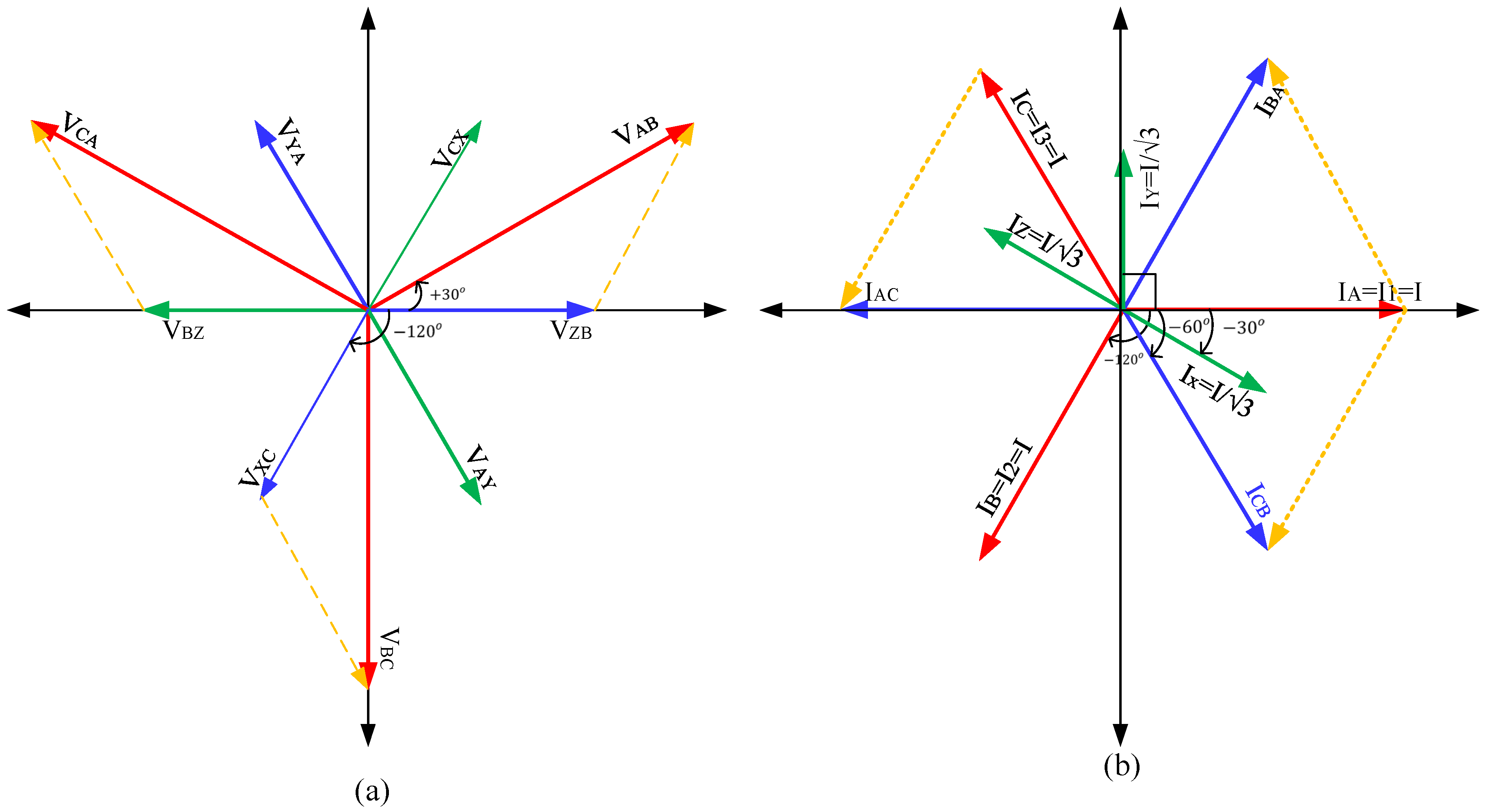
3.1. Analysis of Voltage Relationships
3.2. Analysis of Currents Relationships
3.3. Analysis of Power Relationships
3.4. Loss Analysis
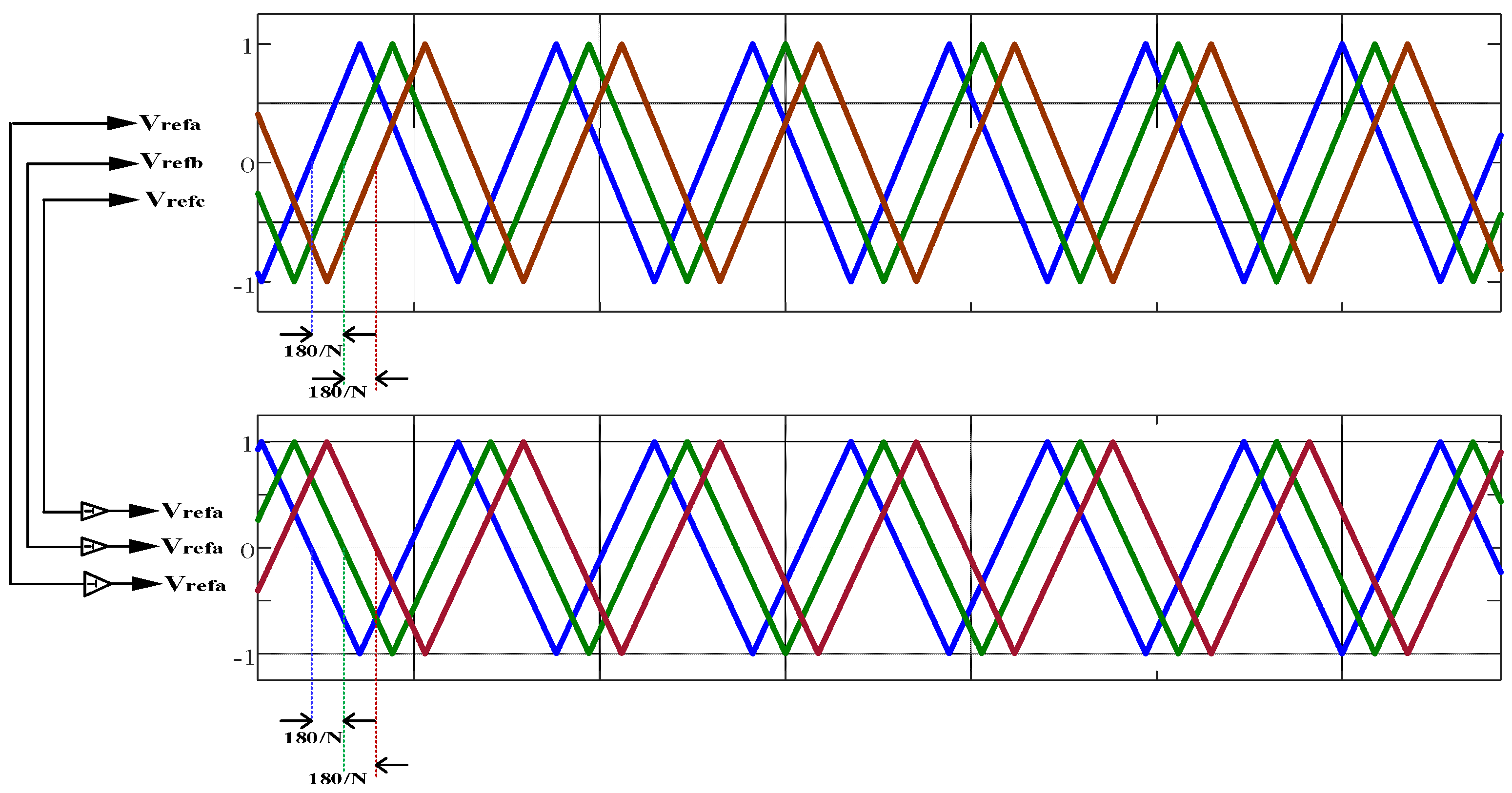
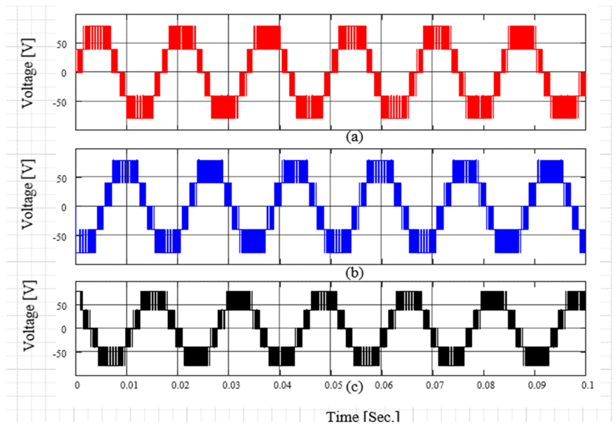
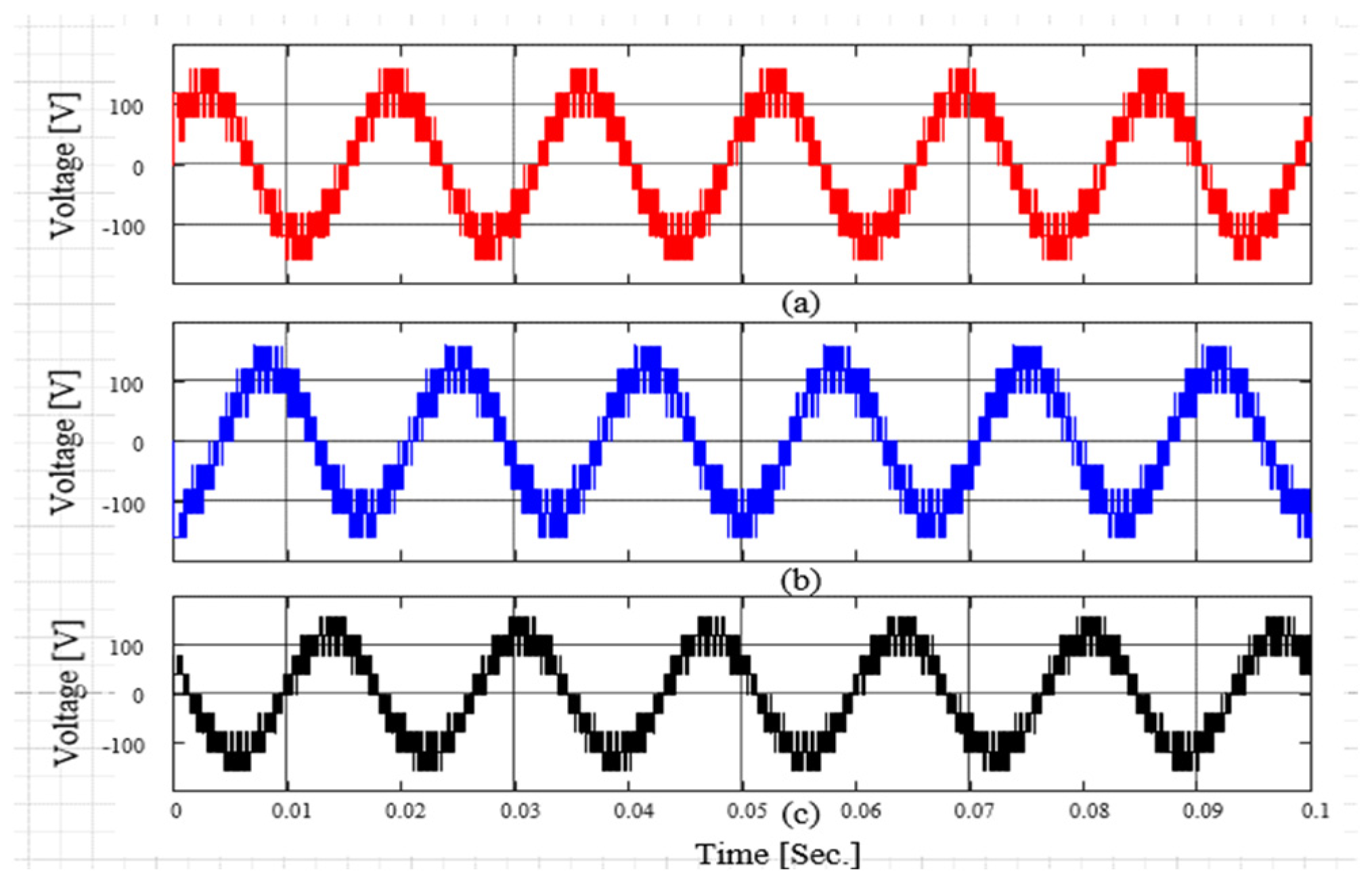
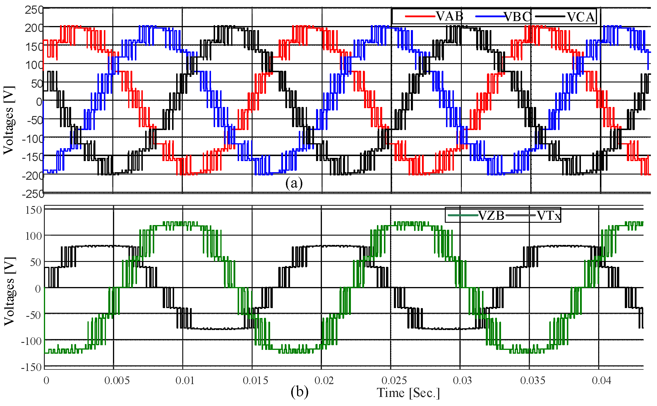
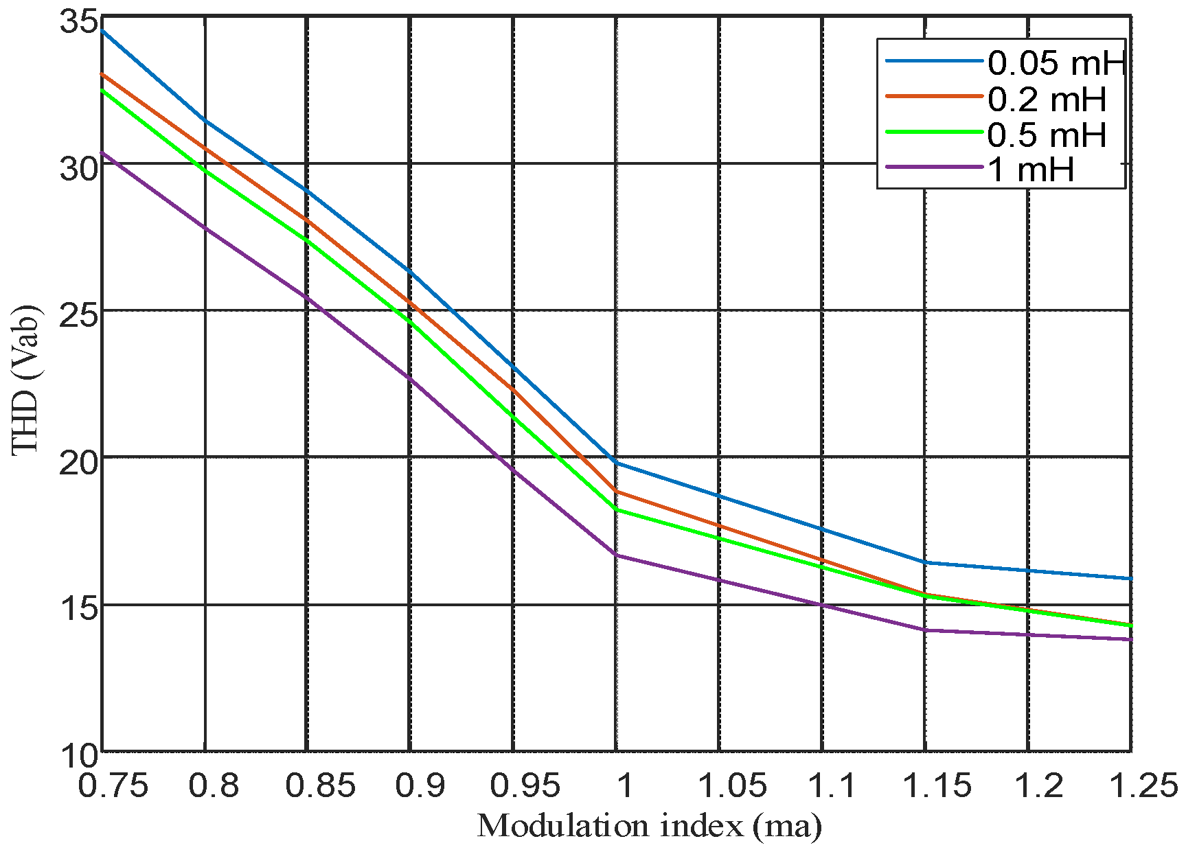
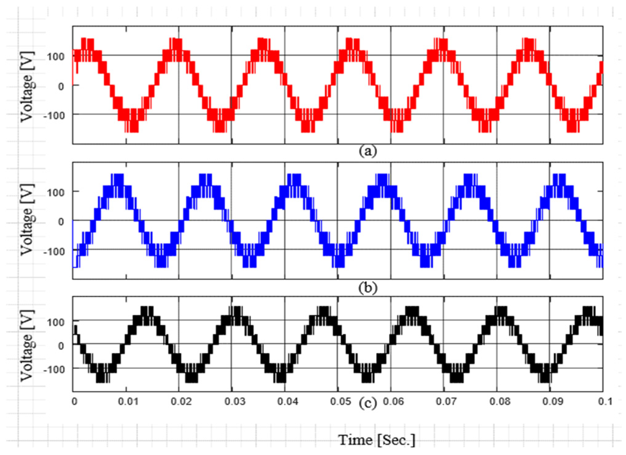
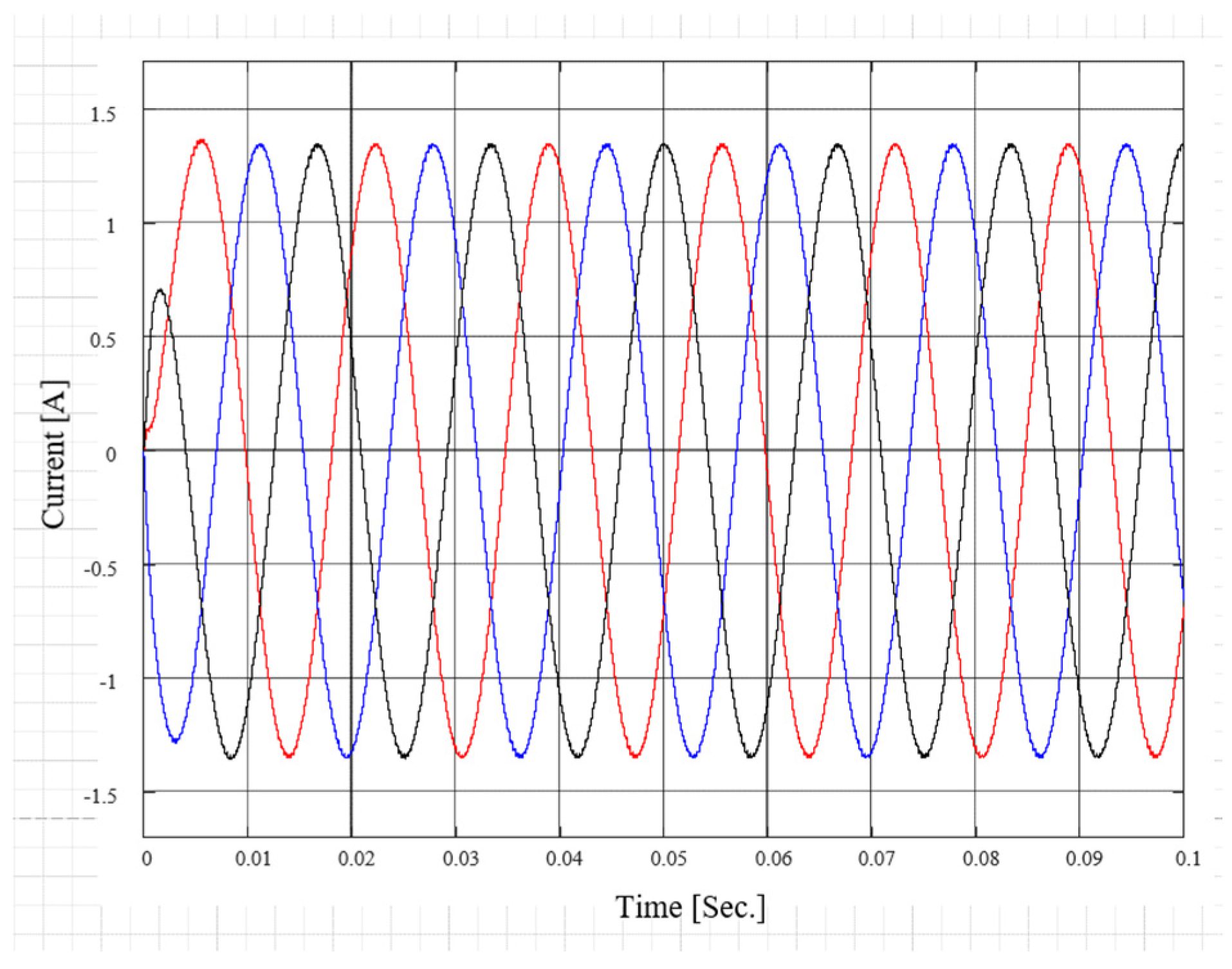
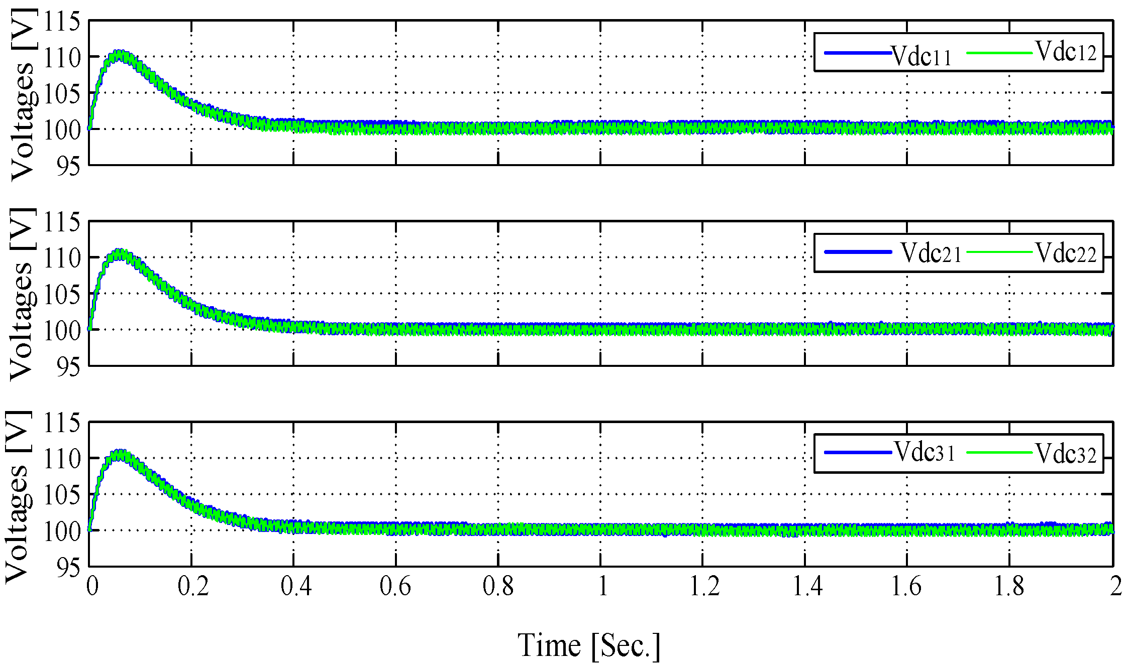
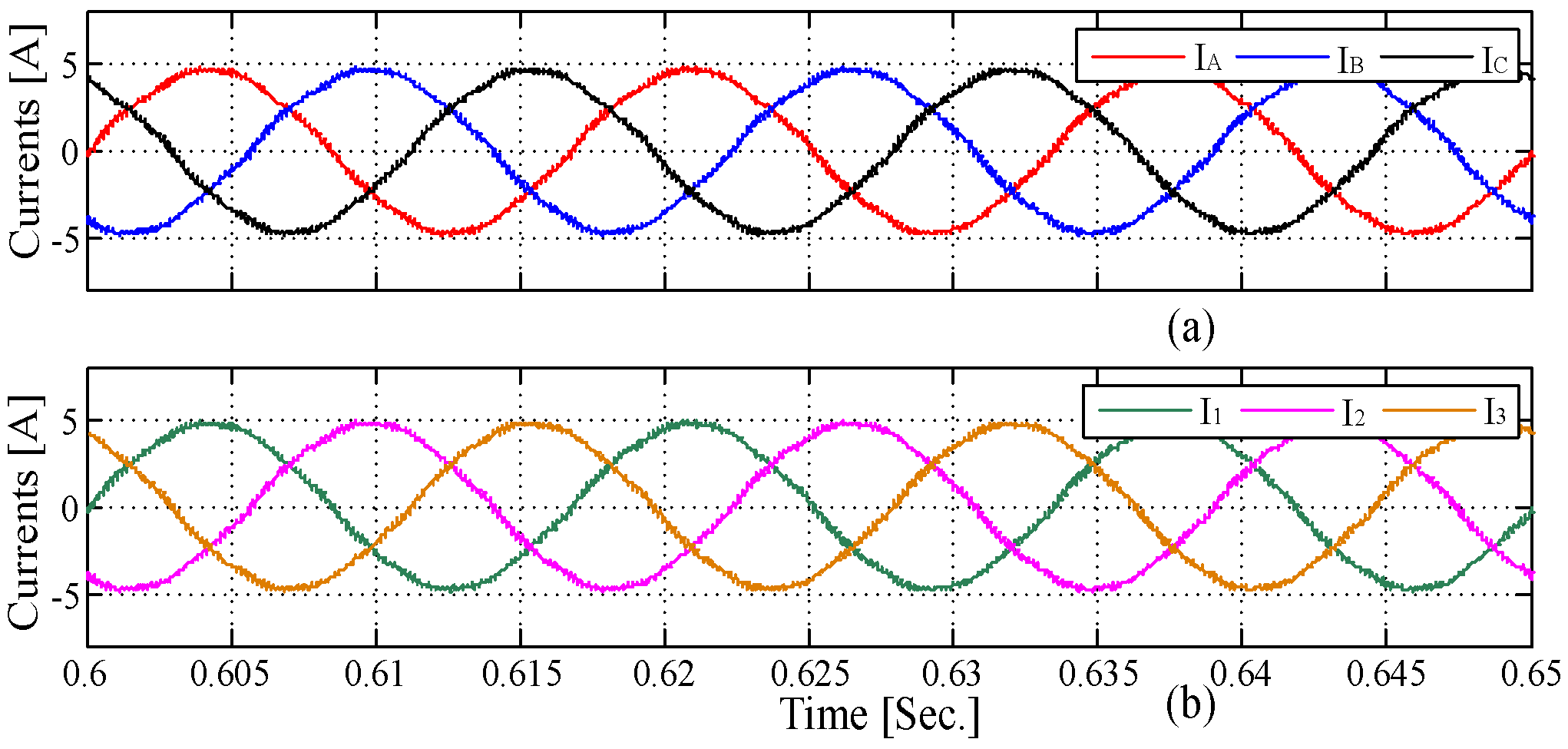
4. Simulation Results
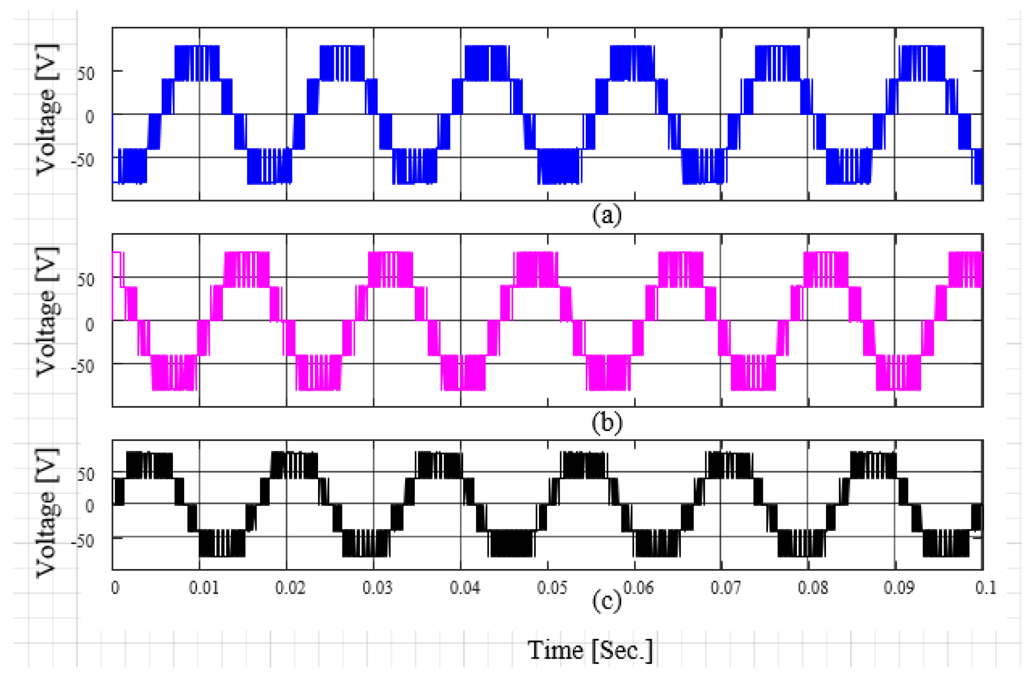
4.1. Open-Loop Test Under a Resistive Load
4.2. Open-Loop Test Under a Resistive–Inductive Load
4.3. PV–Grid Connection Application
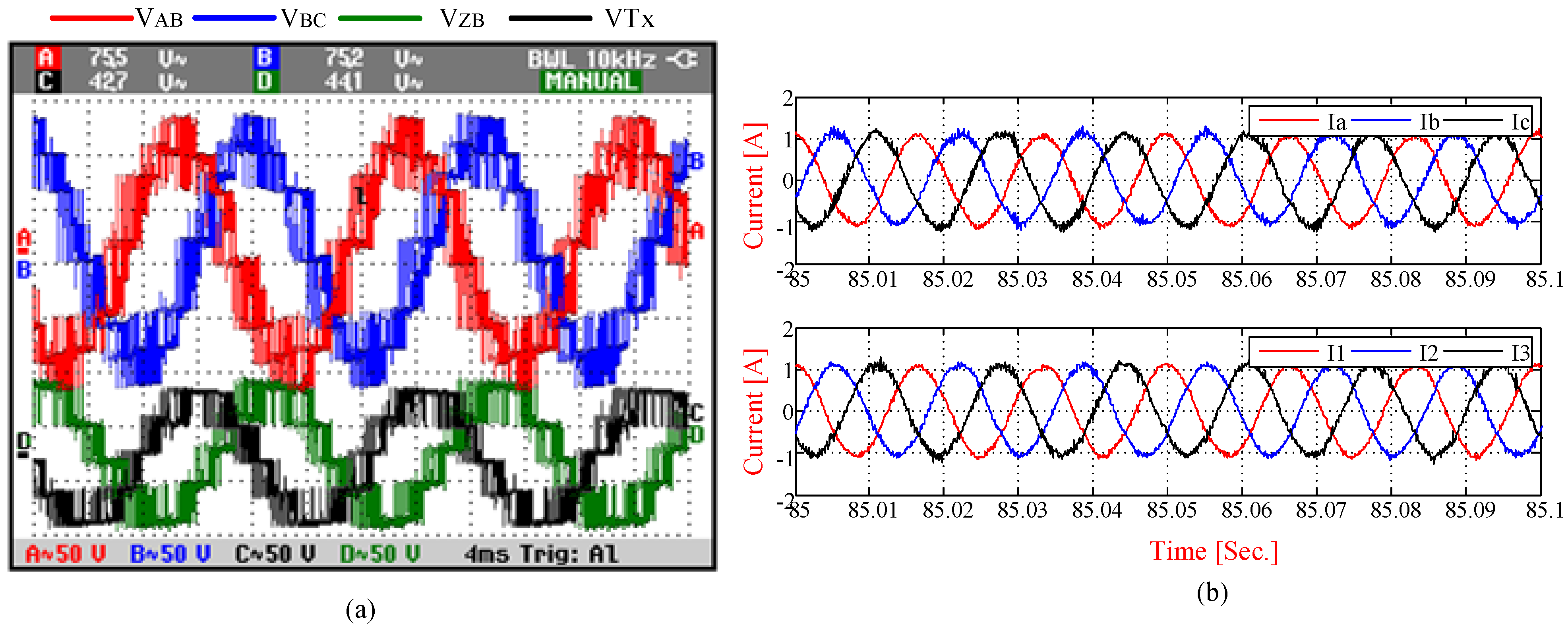
5. Experimental Results
6. Conclusions
Funding
Data Availability Statement
Acknowledgments
Conflicts of Interest
References
- Gupta, K.K.; Ranjan, A.; Bhatnagar, P.; Sahu, L.K.; Jain, S. Multilevel inverter topologies with reduced device count: A review. IEEE Trans. Power Electron. 2015, 31, 135–151. [Google Scholar] [CrossRef]
- Nabae, A.; Takahashi, I.; Akagi, H. A new neutral-point-clamped PWM inverter. IEEE Trans. Ind. Appl. 1981, 5, 518–523. [Google Scholar] [CrossRef]
- Rodriguez, J.; Lai, J.S.; Peng, F.Z. Multilevel inverters: A survey of topologies, controls, and applications. IEEE Trans. Ind. Electron. 2002, 49, 724–738. [Google Scholar] [CrossRef]
- Colak, I.; Kabalci, E.; Bayindir, R. Review of multilevel voltage source inverter topologies and control schemes. Energy Convers. Manag. 2011, 52, 1114–1128. [Google Scholar] [CrossRef]
- Kincic, S.; Chandra, A.; Babic, S. Multilevel inverter and its limitations when applied as statcom. In Proceedings of the 9th Mediterranean conference on control and automation, Dubrovnik, Croatia, 27–29 June 2001. [Google Scholar]
- Daher, S.; Schmid, J.; Antunes, F.L.M. Multilevel inverter topologies for stand-alone PV systems. IEEE Trans. Ind. Electron. 2008, 55, 2703–2712. [Google Scholar] [CrossRef]
- Jakkula, S.; Jayaram, N.; Pulavarthi, S.V.K.; Shankar, Y.R.; Rajesh, J. A generalized high gain multilevel inverter for small scale solar photovoltaic applications. IEEE Access 2022, 10, 25175–25189. [Google Scholar] [CrossRef]
- Memon, A.J.; Mahar, M.A.; Larik, A.S.; Shaikh, M.M. A comprehensive review of reduced device count multilevel inverters for pv systems. Energies 2023, 16, 5638. [Google Scholar] [CrossRef]
- Noman, A.M.; Al-Shamma’A, A.A.; Asef, P.; Alkuhayli, A. Hybrid cascaded MLI development for PV-grid connection applications. IET Power Electron. 2023, 16, 1717–1731. [Google Scholar] [CrossRef]
- Noman, A.M.; Alkuhayli, A.; Al-Shamma’a, A.A.; Addoweesh, K.E. Hybrid MLI Topology Using Open-End Windings for Active Power Filter Applications. Energies 2022, 15, 6434. [Google Scholar] [CrossRef]
- Yousefizad, S.; Azimi, E.; Nasiri-Zarandi, R.; Hafezi, H. A cascaded multilevel inverter based on new basic units. Int. J. Electron. 2022, 109, 2158–2177. [Google Scholar] [CrossRef]
- Seifi, A.; Hosseinpour, M.; Hosseini, S.H. Applications. A novel bidirectional modular multilevel inverter utilizing diode-based bidirectional unit. J. Circuit Theory Appl. 2023, 51, 3226–3245. [Google Scholar] [CrossRef]
- Balal, A.; Dinkhah, S.; Shahabi, F.; Herrera, M.; Chuang, Y.L. A review on multilevel inverter topologies. Emerg. Sci. J. 2022, 6, 185–200. [Google Scholar] [CrossRef]
- Venkataramanaiah, J.; Suresh, Y.; Panda, A.K. A review on symmetric, asymmetric, hybrid and single DC sources based multilevel inverter topologies. Renew. Sustain. Energy Rev. 2017, 76, 788–812. [Google Scholar] [CrossRef]
- Malinowski, M.; Gopakumar, K.; Rodriguez, J.; Perez, M.A. A survey on cascaded multilevel inverters. IEEE Trans. Ind. Electron. 2010, 57, 2197–2206. [Google Scholar] [CrossRef]
- Tolbert, L.; Peng, F. Multilevel converters as a utility interface for renewable energy systems. In Proceedings of the IEEE Power Engineering Society Summer Meeting, Seattle, WA, USA, 16–20 July 2000. [Google Scholar]
- Mohan, H.M.; Dash, S.K.; Ram, S.K.; Caesarendra, W. Performance assessment of three-phase PV tied NPC multilevel inverter based UPQC. In Proceedings of the International Conference on Intelligent Controller and Computing for Smart Power (ICICCSP), Hyderabad, India, 21–23 July 2022. [Google Scholar]
- Kurdkandi, N.V.; Marangalu, M.G.; Hemmati, T.; Mehrizi-Sani, A.; Rahimpour, S.; Babaei, E. Five-level NPC based grid-tied inverter with voltage boosting capability and elimnated leakage current. In Proceedings of the 13th Power Electronics, Drive Systems, and Technologies Conference (PEDSTC), Tehran, Iran, 1–3 February 2022. [Google Scholar]
- Salim, C.H. Electronica; Automatica; Series APF based on Five and Seven-level NPC Inverters using Modified PQ Method. Electroteh. Electron. Autom. (EEA) 2023, 71, 22–29. [Google Scholar]
- Latran, M.B.; Teke, A. Investigation of multilevel multifunctional grid connected inverter topologies and control strategies used in photovoltaic systems. Renew. Sustain. Energy Rev. 2015, 42, 361–376. [Google Scholar] [CrossRef]
- Cheng, H.; Zhao, Z.; Wang, C. A Novel Unidirectional Three-Phase Multilevel Rectifier Composed of Star-Connected Three Single-Phase Topology Based on Five-Level Flying Capacitor DC–DC Converter. IEEE Trans. Ind. Electron. 2022, 70, 5493–5503. [Google Scholar] [CrossRef]
- Kampitsis, G.; Batzelis, E.I.; Mitcheson, P.D.; Pal, B.C. A clamping-circuit-based voltage measurement system for high-frequency flying capacitor multilevel inverters. IEEE Trans. Power Electron. 2022, 37, 12301–12315. [Google Scholar] [CrossRef]
- Bouamrane, O.; Khalili, T.; Tyass, I.; Rafik, M.; Raihani, A.; Bahati, L.; Benhala, B. Flying capacitors multilevel inverter: Architecture, control and active balancing. In Proceedings of the International Conference on Energy and Green Computing, Meknes, Morocco, 9–10 December 2021. [Google Scholar]
- Vishvakarma, R.P.; Singh, S.P.; Shukla, T.N. Multilevel inverters and its control strategies: A comprehensive review. In Proceedings of the 2nd International Conference on Power, Control and Embedded Systems, Allahabad, India, 17–19 December 2012. [Google Scholar]
- Rohner, S.; Bernet, S.; Hiller, M.; Sommer, R. Modulation, losses, and semiconductor requirements of modular multilevel converters. IEEE Trans. Ind. Electron. 2009, 57, 2633–2642. [Google Scholar] [CrossRef]
- Pamujula, M.; Ohja, A.; Kulkarni, R.D.; Swarnkar, P. Cascaded ‘H’bridge based multilevel inverter topologies: A review. In Proceedings of the International Conference for Emerging Technology (INCET), Belgaum, India, 5–7 June 2020. [Google Scholar]
- Dhanamjayulu, C.; Girijaprasanna, T. Experimental Implementation of Cascaded H-Bridge Multilevel Inverter with an Improved Reliability for Solar PV Applications. Int. Trans. Electr. Energy Syst. 2023, 2023, 8794874. [Google Scholar] [CrossRef]
- Cao, Y.; Tolbert, L.M. 11-Level cascaded H-bridge grid-tied inverter interface with solar panels. In Proceedings of the Applied Power Electronics Conference and Exposition (APEC), Palm Springs, CA, USA, 21–25 February 2010. [Google Scholar]
- Xiao, B.; Hang, L.; Mei, J.; Riley, C.; Tolbert, L.M.; Ozpineci, B. Modular Cascaded H-Bridge Multilevel PV Inverter with Distributed MPPT for Grid-Connected Applications. IEEE Trans. Ind. Appl. 2015, 51, 1722–1731. [Google Scholar] [CrossRef]
- Choi, H.; Zhao, W.; Ciobotaru, M.; Agelidis, V.G. Large-scale PV system based on the multiphase isolated dc/dc converter. In Proceedings of the 3rd IEEE International Symposium on Power Electronics for Distributed Generation Systems (PEDG), Aalborg, Denmark, 25–28 June 2012. [Google Scholar]
- Rivera, S.; Wu, B.; Kouro, S.; Wang, H.; Zhang, D. Cascaded H-bridge multilevel converter topology and three-phase balance control for large scale photovoltaic systems. In Proceedings of the 3rd IEEE International Symposium on Power Electronics for Distributed Generation Systems (PEDG), Aalborg, Denmark, 25–28 June 2012. [Google Scholar]
- Ozdemir, S.; Altin, N.; Sefa, I. Single stage three level grid interactive MPPT inverter for PV systems. Energy Convers. Manag. 2014, 80, 561–572. [Google Scholar] [CrossRef]
- Vinayaka, B.C.; Prasad, S.N. Modeling and design of five level cascaded h-bridge multilevel inverter with DC/DC boost converter. Int. J. Eng. Res. Appl. 2014, 4, 50–55. [Google Scholar]
- Sivapriya, A.; Kalaiarasi, N. A review on cascaded h-bridge and modular multilevel converter: Topologies, modulation technique and comparative analysis. In Advanced Power Electronics Converters for Future Renewable Energy Systems, 1st ed.; Taylor & Francis Group: London, UK, 2023; pp. 195–222. [Google Scholar]
- Nagarjuna, A.; Kumar, D.; Reddy, B.; Udaykiran, M. Fifteen level cascaded H-bridge multilevel inverter fed induction motor. Int. J. Innov. Technol. Explor. Eng. 2019, 8, 640–645. [Google Scholar] [CrossRef]
- Rivera, S.; Kouro, S.; Wu, B.; Leon, J.I.; Rodriguez, J.; Franquelo, L.G. Cascaded H-bridge multilevel converter multistring topology for large scale photovoltaic systems. In Proceedings of the IEEE International Symposium on Industrial Electronics (ISIE) 2011, Gdansk, Poland, 27–30 June 2011. [Google Scholar]
- Zhao, W.; Choi, H.; Konstantinou, G.; Ciobotaru, M.; Agelidis, V.G. Cascaded H-bridge multilevel converter for large-scale PV grid-integration with isolated DC-DC stage. In Proceedings of the 3rd IEEE International Symposium on Power Electronics for Distributed Generation Systems (PEDG), Aalborg, Denmark, 25–28 June 2012. [Google Scholar]
- Villanueva, E.; Correa, P.; Rodriguez, J.; Pacas, M. Control of a single-phase cascaded H-bridge multilevel inverter for grid-connected photovoltaic systems. IEEE Trans. Ind. Electron. 2009, 56, 4399–4406. [Google Scholar] [CrossRef]
- Li, J.; He, Y.; Liu, J. Research on the Capability of Star-connected CHB-STATCOM to Compensate the Unbalanced Voltage of Power Grid. IEEE Trans. Power Electron. 2025, 40, 8577–8591. [Google Scholar] [CrossRef]
- Tandekar, J.K.; Ojha, A.; Jain, S. Application of CHB-MLI as a Three-Phase Star-Connected Nine-Level Shunt Active Power Filter. In Multilevel Converters, 1st ed.; Ahmad, S., Bakhsh, F.I., Sanjeevikumar, P., Eds.; Wiley: Hoboken, NJ, USA, 2024; pp. 339–360. [Google Scholar]
- Marquez, A.; Leon, J.I.; Vazquez, S.; Franquelo, L.G. Advanced control of a multilevel cascaded H-bridge converter for PV applications. In Proceedings of the 40th Annual Conference of the IEEE Industrial Electronics Society, IECON, Dallas, TX, USA, 29 October–1 November 2014. [Google Scholar]
- Alexander, S. Development of solar photovoltaic inverter with reduced harmonic distortions suitable for Indian sub-continent. Renew. Sustain. Energy Rev. 2016, 56, 694–704. [Google Scholar] [CrossRef]
- Sahoo, S.K.; Bhattacharya, T. Phase-shifted carrier-based synchronized sinusoidal PWM techniques for a cascaded H-bridge multilevel inverter. IEEE Trans. Power Electron. 2017, 33, 513–524. [Google Scholar] [CrossRef]
- Govindaraju, C.; Baskaran, K. Efficient sequential switching hybrid-modulation techniques for cascaded multilevel inverters. IEEE Trans. Power Electron. 2011, 26, 1639–1648. [Google Scholar] [CrossRef]
- Khemili, F.Z.; Bouhali, O.; Lefouili, M.; Chaib, L.; El-Fergany, A.A.; Agwa, A.M. Design of Cascaded Multilevel Inverter and Enhanced MPPT Method for Large-Scale Photovoltaic System Integration. Sustainability 2023, 15, 9633. [Google Scholar] [CrossRef]
- Chang, W.-N.; Liao, C.-H. Design and Implementation of a STATCOM Based on a Multilevel FHB Converter with Delta-Connected Configuration for Unbalanced Load Compensation. Energies 2017, 10, 921. [Google Scholar] [CrossRef]
- Yu, Y.; Konstantinou, G.; Townsend, C.D.; Aguilera, R.P.; Agelidis, V.G. Delta-Connected Cascaded H-Bridge Multilevel Converters for Large-Scale Photovoltaic Grid Integration. IEEE Trans. Ind. Electron. 2017, 64, 8877–8886. [Google Scholar] [CrossRef]
- Yu, Y.; Konstantinou, G.; Townsend, C.D.; Aguilera, R.P.; Hredzak, B.; Agelidis, V.G. Delta-connected cascaded H-bridge multilevel photovoltaic converters. In Proceedings of the 41st Annual Conference of Industrial Electronics Society, Yokohama, Japan, 9–12 November 2015. [Google Scholar]
- Wen, J.; Smedley, K.M. Synthesis of multilevel converters based on single-and/or three-phase converter building blocks. IEEE Trans. Power Electron. 2008, 23, 1247–1256. [Google Scholar] [CrossRef]
- Peng, F.Z.; Wang, J. A universal STATCOM with delta-connected cascade multilevel inverter. In Proceedings of the 35th IEEE Power Electronics Specialists Conference, Aachen, Germany, 20–25 June 2004. [Google Scholar]
- Zhixing, H.; Fujun, M.; An, L.; Qianming, X.; Yandong, C.; Huagen, X.; Guobin, J. Circulating current derivation and comprehensive compensation of cascaded STATCOM under asymmetrical voltage conditions. IET Gener. Transm. Distrib. 2016, 10, 2924–2932. [Google Scholar] [CrossRef]
- Babu, N.S.; Al Hosani, K. A novel DC voltage control for a cascade H-bridge multilevel STATCOM. In Proceedings of the 41st Annual Conference of the IEEE Industrial Electronics Society IECON, Yokohama, Japan, 9–12 November 2015. [Google Scholar]
- Jung, J.-J.; Lee, J.-H.; Sul, S.-K.; Son, G.T.; Chung, Y.-H. DC Capacitor Voltage Balancing Control for Delta-Connected Cascaded H-Bridge STATCOM Considering Unbalanced Grid and Load Conditions. IEEE Trans. Power Electron. 2018, 33, 4726–4735. [Google Scholar] [CrossRef]
- Padiyar, K.R.; Kulkarni, A.M. Modeling and analysis of FACTS and HVDC controllers. In Dynamics and Control of Electric Transmission and Microgrids, 1st ed.; Padiyar, K.R., Kulkarni, A.M., Eds.; Wiley: Hoboken, NJ, USA, 2019. [Google Scholar]
- Akagi, H. Classification, terminology, and application of the modular multilevel cascade converter (MMCC). IEEE Trans. Power Electron. 2011, 26, 3119–3130. [Google Scholar] [CrossRef]
- Molinas, M.; Suul, J.A.; Undeland, T. Low voltage ride through of wind farms with cage generators: STATCOM versus SVC. IEEE Trans. Power Electron. 2008, 23, 1104–1117. [Google Scholar] [CrossRef]
- Mohammadi, P.H.; Bina, M.T. A transformerless medium-voltage STATCOM topology based on extended modular multilevel converters. IEEE Trans. Power Electron. 2010, 26, 1534–1545. [Google Scholar]
- Liang, Y.; Nwankpa, C. A new type of STATCOM based on cascading voltage-source inverters with phase-shifted unipolar SPWM. IEEE Trans. Ind. Appl. 1999, 35, 1118–1123. [Google Scholar] [CrossRef]
- Lee, C.; Leung, J.; Hui, S.; Chung, H.-H. Circuit-level comparison of STATCOM technologies. IEEE Trans. Power Electron. 2003, 18, 1084–1092. [Google Scholar] [CrossRef]
- Marzo, I.; Sanchez-Ruiz, A.; Barrena, J.A.; Abad, G.; Muguruza, I. Power balancing in cascaded H-bridge and modular multilevel converters under unbalanced operation: A review. IEEE Access 2021, 9, 110525–110543. [Google Scholar] [CrossRef]
- Hameed, U.; Sadiq, H.; Khalid, H.A.; Khan, M.U.; Ali, M. Investigation of zero sequence injection method for balancing of multi-level Cascaded-H bridge inverter. In Proceedings of the IEEE International Conference on Computing, Electronic and Electrical Engineering, Quetta, Pakistan, 12–13 November 2018. [Google Scholar]
- He, Z.; Ma, F.; Xu, Q.; Chen, Y.; Li, C.; Li, M.; Guerrero, J.M.; Luo, A. Reactive power strategy of cascaded delta-connected STATCOM under asymmetrical voltage conditions. IEEE J. Emerg. Sel. Top. Power Electron. 2017, 5, 784–795. [Google Scholar] [CrossRef]
- Wu, P.-H.; Chen, H.-C.; Chang, Y.-T.; Cheng, P.-T. Delta-connected cascaded H-bridge converter application in unbalanced load compensation. IEEE Trans. Ind. Appl. 2016, 53, 1254–1262. [Google Scholar] [CrossRef]
- Liu, H.; Tolbert, L.M.; Khomfoi, S.; Ozpineci, B.; Du, Z. Hybrid cascaded multilevel inverter with PWM control method. In Proceedings of the Power Electronics Specialists Conference, Rhodes, Greece, 15–19 June 2008. [Google Scholar]
- Kangarlu, M.F.; Babaei, E. A generalized cascaded multilevel inverter using series connection of submultilevel inverters. IEEE Trans. Power Electron. 2012, 28, 625–636. [Google Scholar] [CrossRef]
- Gandomi, A.A.; Saeidabadi, S.; Hosseini, S.H.; Babaei, E.; Sabahi, M. Transformer-based inverter with reduced number of switches for renewable energy applications. IET Power Electron. 2015, 8, 1875–1884. [Google Scholar] [CrossRef]


| Topology | NPC | FC | CHB (Star) | CHB (Delta) | Proposed Topology |
|---|---|---|---|---|---|
| Main switches | 24 | 24 | 24 | 48 | 24 |
| Clamping diodes | 36 | 0 | 0 | 0 | 0 |
| Flying capacitors | 0 | 18 | 0 | 0 | 0 |
| Dc link capacitors | 4 | 4 | 6 | 12 | 6 |
| Intermediate inductors | 0 | 0 | 0 | 3 | 0 |
| Intermediate transformers | 0 | 0 | 0 | 0 | 3 |
| DC sources | 1 | 1 | 6 | 12 | 6 |
| Modularity | No | No | Yes | Yes | Yes |
| Inherent voltage balancing capability | No | No | Yes | Yes | Yes |
| Required grid-side transformer (if necessary) | Yes | Yes | Yes | Yes | No |
| Load resistance and inductance (for the R and L testing) | 48 Ω, 77 mH |
| DC input voltage (for the R and L testing) | 40 V |
| RMS grid voltage | 120 V |
| Grid interface inductance | 2.5 mH |
| Fundamental frequency | 60 Hz |
| 900 Hz |
| Maximum power (Pmax) | 245 W |
| Maximum power voltage (Vmax) | 28.8 V |
| Maximum power current (Imax) | 8.5 A |
| Open-circuit voltage (Voc) | 31.5 V |
| Short-circuit current (Isc) | 9.5 A |
| Load resistance | 48 Ω |
| Load inductance | 77 mH |
| 900 Hz | |
| Three coupled transformers | Part No. 810.1201 Each: 230 V, 1.5 KVA |
| IGBTs | Part No. SKM75GB12V |
| IGBT drives | Part No. SKYPER 32 R |
| PV modules | Part No. KACST 245 |
Disclaimer/Publisher’s Note: The statements, opinions and data contained in all publications are solely those of the individual author(s) and contributor(s) and not of MDPI and/or the editor(s). MDPI and/or the editor(s) disclaim responsibility for any injury to people or property resulting from any ideas, methods, instructions or products referred to in the content. |
© 2025 by the author. Licensee MDPI, Basel, Switzerland. This article is an open access article distributed under the terms and conditions of the Creative Commons Attribution (CC BY) license (https://creativecommons.org/licenses/by/4.0/).
Share and Cite
Noman, A.M. A Novel Modified Delta-Connected CHB Multilevel Inverter with Improved Line–Line Voltage Levels. Electronics 2025, 14, 1711. https://doi.org/10.3390/electronics14091711
Noman AM. A Novel Modified Delta-Connected CHB Multilevel Inverter with Improved Line–Line Voltage Levels. Electronics. 2025; 14(9):1711. https://doi.org/10.3390/electronics14091711
Chicago/Turabian StyleNoman, Abdullah M. 2025. "A Novel Modified Delta-Connected CHB Multilevel Inverter with Improved Line–Line Voltage Levels" Electronics 14, no. 9: 1711. https://doi.org/10.3390/electronics14091711
APA StyleNoman, A. M. (2025). A Novel Modified Delta-Connected CHB Multilevel Inverter with Improved Line–Line Voltage Levels. Electronics, 14(9), 1711. https://doi.org/10.3390/electronics14091711