Communication

A 6–18 GHz Low-Noise Amplifier with 19 dBm OP1dB and 2.6 ± 0.3 dB NF in 0.15 μm GaAs Process

1
State Key Laboratory of Optoelectronic Materials and Devices, Institute of Semiconductors, Chinese Academy of Sciences, Beijing 100083, China
2
College of Materials Science and Optoelectronic Technology, University of Chinese Academy of Sciences, Beijing 100049, China
*
Author to whom correspondence should be addressed.
Electronics 2025, 14(8), 1600; https://doi.org/10.3390/electronics14081600
Submission received: 12 March 2025 / Revised: 3 April 2025 / Accepted: 11 April 2025 / Published: 15 April 2025

Abstract

:
A three-stage low-noise amplifier (LNA) operating over the 6–18 GHz frequency range is designed and implemented, featuring a flat noise figure (NF) and enhanced output 1 dB compression point (OP1dB). To improve linearity and minimize distortion, a power high-electron-mobility transistor (HEMT) is employed in the final stage. Additionally, resistive feedback and self-biasing techniques are integrated to extend the amplifier’s bandwidth. The proposed LNA exhibits a high and flat power gain of 25 ± 1 dB, with an input return loss of more than 10 dB. The measured NF remains stable at 2.6 ± 0.3 dB over the 6–18 GHz range. Furthermore, the OP1dB exceeds 19.5 dBm across the entire 3 dB gain bandwidth (BW). The circuit is fabricated using a 0.15 μm GaAs pHEMT process, occupying a compact chip area of 1.2 × 1.8 mm2.

1. Introduction

Ultra-wideband (UWB) communication systems operating within the 3.1–10.6 GHz spectrum demonstrate broad applicability in diverse fields, including high-resolution radar systems, precision instrumentation, short-range communication, and high-speed transceiver architectures [1,2]. As the first active module in a UWB receiver, the low-noise amplifier (LNA) is a key component whose noise figure, gain, linearity, and bandwidth considerably influence receiver sensitivity. Recent studies have indicated that GaAs technology is well suited for the design of LNAs. GaAs achieves a better balance of low noise figure, high linearity, and compact footprint at a relatively low cost [3]. This makes it an excellent choice for applications where both high performance and cost-effectiveness are crucial. In modern radar and communication systems, LNAs must simultaneously handle weak signals and strong interference, necessitating high OP1dB to maintain linearity and prevent distortion under dynamic conditions. However, current LNAs do not have sufficiently high OP1dB, which renders them unable to meet the various requirements of multiple frequency bands and higher standards. Consequently, it is crucial to design a broadband LNA with high OP1dB, which is of great research significance.
In recent years, researchers have reported several approaches to extending the bandwidth of LNAs, including distributed topologies, inductive peaking, and resistive feedback techniques. Distributed topologies can achieve significant bandwidth extension [4,5]. However, their practical implementation faces constraints including excessive component footprint, poor noise figure, and high power consumption. The inductive peaking technique [6], though effective for frequency response improvement, similarly requires a large chip area. In contrast, resistive feedback topologies have been extensively reported [7] as a space-efficient bandwidth expansion solution. Hybrid microwave integrated circuits (HMICs) offer a distinct alternative [8], achieving compact size, low noise figure, and optical sensing capability, but their bandwidth is limited by lumped-element matching and they are sensitive to environmental factors like light exposure. According to the above literature research, few LNAs have been reported to operate across the C- to Ku-bands with NF below 3 dB, power gain over 20 dB, and OP1dB over 10 dBm.
In this paper, a broadband three-stage LNA with a flat NF and high OP1dB is proposed, addressing the critical challenge of achieving high linearity, wide bandwidth, and low noise figure across the 6–18 GHz spectrum. By leveraging a power high-electron-mobility transistor (HEMT) in the final stage and optimizing the output matching network, the design achieves a record-high OP1dB of 19.5 dBm across the entire operational bandwidth. Furthermore, to extend bandwidth while maintaining flat gain and noise performance, resistive feedback networks are employed in the latter two stages, expanding the 3 dB bandwidth (BW) to 12.9 GHz (5.7–18.6 GHz) and ensuring a flat NF of 2.6 ± 0.3 dB and gain of 25 ± 1 dB. Additionally, a self-biasing architecture reduces the chip area to 1.2 × 1.8 mm2 and eliminates the need for dual power supplies, overcoming the multi-power supply complexity and large footprint issues. The LNA’s high OP1dB and wide bandwidth enable dual-use in both receive and transmit chains, thereby broadening the scope of potential applications and offering a compact, high-performance solution for applications including military radars, wireless communication systems, and broadband instrumentation (such as spectrum analyzers and vector network analyzers).

2. LNA Circuit Design

2.1. Topology of the LNA

The schematic of the proposed three-stage LNA is presented in Figure 1. Self-biasing technology is adopted in all stages, in which RS1/CS1/L3 participate in M1 biasing. The gate of M1 is biased to the ground by inductor L3, and the source terminal is biased by resistor RS1. The principle behind this self-biasing technique is that the source resistor RS1 raises the source potential of the transistor M1. With the gate grounded via the inductor L3, a gate–source voltage VGS of −0.6 V is generated without the need for a negative power supply. Based on the bias condition of M1, analogous voltage distributions can be derived for the gate and drain bias of M2/M3. The parallel capacitor CS1 plays a crucial role in circuit performance. Due to the frequency response of the capacitors, CS1 can bypass low-frequency signals, reducing low-frequency resonance. By suppressing low-frequency resonance, CS1 helps to stabilize the gain across the frequency band, thereby improving the gain flatness. Moreover, it optimizes the impedance characteristics of the circuit, reducing oscillations and enhancing the overall stability of the circuit. For the three-stage amplifier design, the values of the source resistors RS are determined by the bias currents IDD. Given that the LNA is biased at VGS = −0.6 V and the total bias current is 180 mA (I1 = 20 mA, I2 = 70 mA, I3 = 90 mA), we can calculate that RS1 = 30 Ω, RS2 = 9 Ω, and RS3 = 7 Ω. Self-biasing technology effectively reduces the number of power supplies from two (1 gate, 1 drain) to a single supply, minimizes power pads, and decreases the chip footprint. In addition, the resistive feedback technique is utilized in the latter two stages. The resistive feedback network comprises a resistor Rf and a blocking capacitor Cf, forming a negative feedback path between the gate and the drain. The function of this particular negative feedback path is to suppress low-frequency gain, thereby achieving a flat broadband response and enhancing stability, which leads to an expansion of the bandwidth.
A basic guideline is given regarding the circuit design: low NF is the key parameter for the first stage, while high linearity is the main index for the third stage. Inter-stage impedance matchings achieve an overall flat gain response. Hence, the first two stages of the circuit are designed with low-noise HEMTs, and the final stage uses a power HEMT with higher linearity, which significantly improves the OP1dB of the LNA while maintaining high gain and low noise. What is more, the widths of transistors are selected as WM1 = 4 × 30 μm, WM2 = 6 × 55 μm, and WM3 = 6 × 80 μm. The width of the transistor is gradually increased from the first to the third stage to improve OP1dB while saving power consumption. Since the NF of the first stage dominates the LNA’s overall NF, minimizing its noise contribution is critical. The bias voltage of the first-stage transistor is adjusted to 2 V through the insertion of a series resistance R1 in its drain bias path, which suppresses short-channel effects and minimizes the NFmin of the first stage. In addition, inductor L3 participates in forming a reactive impedance π-matching network with inductors L1 and L2, approximating the optimal noise impedance while balancing wideband input standing-wave ratio (VSWR) performance. At the same time, the linearity of the final stage contributes more to the overall linearity of the amplifier [9]. The output matching network is formed with capacitor C6 and inductors L11 to achieve output impedance matching and a trade-off between OP1dB and the standing wave. Resistor R3 improves stability at the cost of consuming output power.

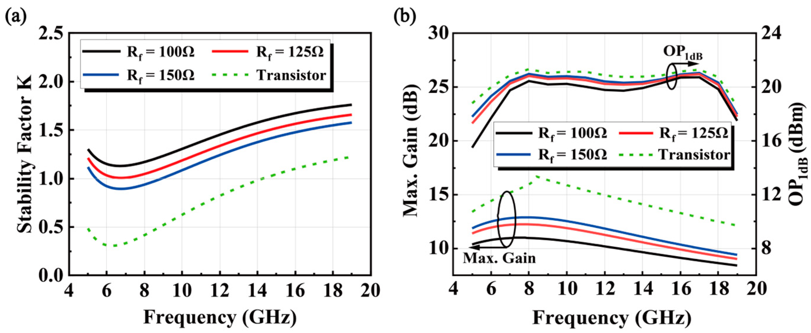
2.2. Resistive Feedback Technique

The resistive feedback technique is utilized in the last two stages, enhancing circuit stability while moderately reducing broadband gain. However, it is unsuitable for the LNA input stage. The feedback resistance Rf would significantly increase the noise figure because of its inherent thermal noise. Since the first stage plays a dominant role in the LNA’s overall noise performance, excluding Rf here is essential to minimize the noise figure, ensuring the LNA meets the low-noise design requirement. Figure 1 illustrates the optimized feedback network (highlighted in red). The capacitor Cf, assigned a substantial capacitance value of 2 pF, effectively minimizes its influence on the system’s frequency characteristics. This capacitor primarily serves as a DC blocking component to maintain proper bias isolation between the transistor’s gate and drain terminals, ensuring stable operating conditions.
Figure 2 comparatively demonstrates three critical performance parameters, maximum gain, output 1 dB compression point (OP1dB), and stability factor k, for both the standalone transistor and the third-stage feedback amplifier. Furthermore, we evaluate how variations in the feedback resistance Rf influence the frequency response of the circuit. It can be seen that as the resistor Rf increases, the maximum gain and OP1dB increase and the stability factor k decreases. The feedback amplifier circuit improves the stability of the circuit and prevents the circuit from generating self-excitation. At the same time, although the feedback amplifier circuit reduces the maximum gain and OP1dB by decreasing the amplitude of the input signal of the transistor, it suppresses the low-frequency gain and greatly improves the gain flatness. The circuit’s unconditional stability condition (k > 1) requires Rf ≤ 125 Ω. Through comprehensive trade-off analysis, the feedback resistance value was established at 125 Ω, achieving balanced performance characteristics. After completing the design of the input and output matching networks, the circuit’s stability factor k will be further improved, ensuring the circuit achieves unconditionally stable operation.

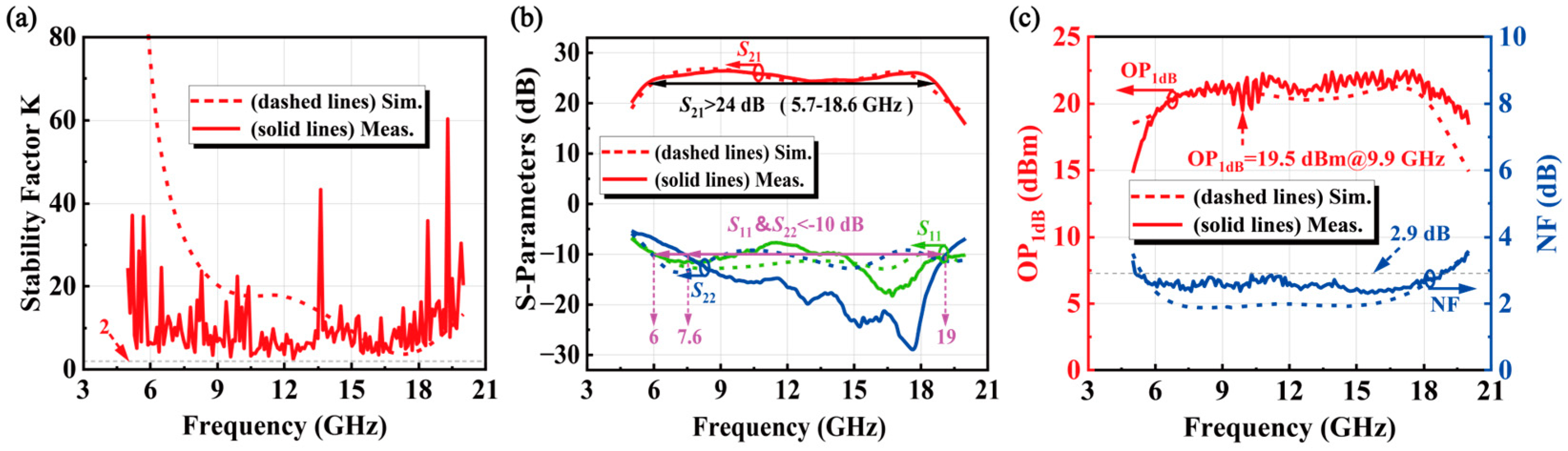
3. Results and Discussion

The proposed LNA is fabricated using a 0.15 µm GaAs pHEMT process with a chip size of 1.8 × 1.2 mm2. Figure 3 presents the annotated chip micrograph. The S-parameters, OP1dB, and NF of this LNA are measured using Keysight PNA-X N5247B via on-wafer probing. As shown in Figure 4a, the measured stability factor k of the LNA exceeds 2 across the entire 5–20 GHz band, confirming absolute stability. Comparative results between simulated and measured S-parameters are illustrated in Figure 4b, where the LNA exhibits a maximum gain of 26.4 dB at 9 GHz and a 3 dB bandwidth (BW) spanning 5.7–18.6 GHz. Input/output matching performance demonstrates broadside optimization, with the measured S11 remaining below −9 dB across 6–19 GHz and S22 suppressed under −10 dB from 7.6 to 19 GHz. In addition, Figure 4c provides the measured and simulated NF and OP1dB. It can be seen that the measured NF is below 2.9 dB over 5–19 GHz and OP1dB exceeds 19.5 dBm within the 6–19 GHz operational bandwidth. Table 1 summarizes the key performance of LNAs for quantitative evaluation. To better evaluate the LNA’s performance, a widely adopted figure of merit (FOM) is employed, incorporating critical parameters including power gain, noise figure, BW, DC power consumption, and linearity (P1dB). The FOM is defined as follows [10]:
FOM = Gain max dB × BW ( GHz ) × P 1 dB ( mW ) ( N F mean 1 ) × P DC ( mW )
In comparison with other work, the proposed LNA achieves a low and flat NF response (competitive with [5,11]), delivers a 25 dB gain surpassing those of [5,12], and reaches the highest OP1dB of 21 dBm among these works for superior linearity. Despite the higher PDC, the LNA achieves the highest FOM, effectively balancing gain, noise, bandwidth, linearity, and power consumption. Overall, the proposed low-noise amplifier demonstrates advantages in key parameters, achieving a low and flat NF, high power gain, the highest OP1dB, and a competitive FOM.

4. Conclusions

In this paper, a broadband LNA with high OP1dB is presented. The LNA is implemented in a 0.15 μm GaAs pHEMT process. It achieves 12–18 GHz bandwidth, 25 ± 1 dB gain, and 2.6 ± 0.3 dB NF. The OP1dB is greater than 19.5 dBm over the entire 3 dB gain BW. This design’s combination of high OP1dB, low NF, and wide bandwidth makes it suitable for applications such as military radar jamming mitigation, multi-user communication, and broadband instrumentation, where robust signal handling and integration density are critical.

Author Contributions

Conceptualization, X.W., T.M. and B.C.; data curation, X.W.; formal analysis, X.W. and T.M.; investigation, X.W.; methodology, X.W. and T.M.; software, X.W. and Tao Men; validation, X.W.; writing—original draft, X.W.; writing–review and editing, X.W., T.M. and B.C. All authors have read and agreed to the published version of the manuscript.

Funding

This research received no external funding.

Data Availability Statement

The original contributions presented in this study are included in the article. Further inquiries can be directed to the corresponding author(s).

Conflicts of Interest

The authors declare no conflicts of interest.

References

  1. Shan, L.Q.; Hu, Y.T.; Zhang, F.H.; Chen, M. Resource Allocation for Multicarrier Communication in the Finite Blocklength Regime. IEEE Wirel. Commun. Lett. 2023, 12, 1771–1775. [Google Scholar] [CrossRef]
  2. Nikandish, G.; Yousefi, A.; Kalantari, M. A Broadband Multistage LNA With Bandwidth and Linearity Enhancement. IEEE Microw. Wirel. Compon. Lett. 2016, 26, 834–836. [Google Scholar] [CrossRef]
  3. Jiang, Y.; Su, G.-D.; Sun, D.; Huang, Y.; Lin, Z.; Liu, J. GaAs based MMIC LNA for X-band Applications. In Proceedings of the 2022 IEEE MTT-S International Microwave Workshop Series on Advanced Materials and Processes for RF and THz Applications (IMWS-AMP), Guangzhou, China, 12–14 December 2022; pp. 1–3. [Google Scholar]
  4. Mesgari, B.; Saeedi, S.; Jannesari, A. Cell Weighting and Gate Inductive Peaking Techniques for Wideband Noise Suppression in Distributed Amplifiers. IEEE Trans. Circuits Syst. I Regul. Pap. 2020, 67, 4507–4520. [Google Scholar] [CrossRef]
  5. Yan, X.; Luo, H.; Zhang, J.; Zhang, H.; Guo, Y. Design and Analysis of a Cascode Distributed LNA With Gain and Noise Improvement in 0.15-m GaAs pHEMT Technology. IEEE Trans. Circuits Syst. II Express Briefs 2022, 69, 4659–4663. [Google Scholar] [CrossRef]
  6. Li, N.; Feng, W.; Li, X. A CMOS 3-12-GHz Ultrawideband Low Noise Amplifier by Dual-Resonance Network. IEEE Microw. Wirel. Compon. Lett. 2017, 27, 383–385. [Google Scholar] [CrossRef]
  7. Wang, Z.; Chen, J.; Hou, D.; Zhou, P.; Chen, Z.; Wang, L.; Xu, X.; Hong, W. A 1-27 GHz SiGe Low Noise Amplifier With 27-dB Peak Gain and 2.85 ± 1.45 dB NF. IEEE Trans. Circuits Syst. II Express Briefs 2024, 71, 2629–2633. [Google Scholar] [CrossRef]
  8. Caddemi, A.; Cardillo, E.; Patanè, S.; Triolo, C. An Accurate Experimental Investigation of an Optical Sensing Microwave Amplifier. IEEE Sens. J. 2018, 18, 9214–9221. [Google Scholar] [CrossRef]
  9. Razavi, B. RF Microelectronics, 2nd ed.; Prentice-Hall: Englewood Cliffs, NJ, USA, 2011. [Google Scholar]
  10. Wang, L.; Cheng, Y.J. A 2-20-GHz Ultrawideband High-Gain Low-Noise Amplifier With Enhanced Stability. IEEE Microw. Wirel. Compon. Lett. 2024, 34, 415–418. [Google Scholar] [CrossRef]
  11. Li, J.X.; Yuan, Y.; Zeng, J.L.; He, D.; Yu, Z.J. A Broadband LNA With Multiple Bandwidth Enhancement Techniques. IEEE Microw. Wirel. Technol. Lett. 2023, 33, 551–554. [Google Scholar] [CrossRef]
  12. Cheng, X.; Zhang, L.; Chen, F.-J.; Deng, X. A broadband GaAs pHEMT low noise driving amplifier with current reuse and self-biasing technique. Analog. Integr. Circuits Signal Process. 2019, 99, 191–198. [Google Scholar] [CrossRef]
  13. Yang, Z.; Wang, K.S.; Fan, Y.H.; Yan, Y.P.; Liang, X.X. Design of a GaAs-Based Ka-Band Low Noise Amplifier MMIC with Gain Flatness Enhancement. Electronics 2023, 12, 2325. [Google Scholar] [CrossRef]
  14. Chen, Y.M.; Wang, Y.S.; Chiong, C.C.; Wang, H. A 21.5-50 GHz Low Noise Amplifier in 0.15-μm GaAs pHEMT Process for Radio Astronomical Receiver System. In Proceedings of the IEEE Asia-Pacific Microwave Conference (APMC), Electr Network, Brisbane, QLD, Australia, 28 November–1 December 2021; pp. 7–9. [Google Scholar]
  15. Babenko, A.A.; Lasser, G.; Popovic, Z. 0.01-22-GHz Feedback-Stabilized Single-Supply GaAs Cascode Distributed Amplifiers. IEEE Microw. Wirel. Compon. Lett. 2021, 31, 1291–1294. [Google Scholar] [CrossRef]
Figure 1. Schematic of the LNA.
Electronics 14 01600 g001
Figure 2. Simulated (a) stability factor k and (b) maximum gain and output 1 dB compression points for the transistor and the feedback amplifier.
Electronics 14 01600 g002
Figure 3. Chip micrograph of the LNA.
Electronics 14 01600 g003
Figure 4. Simulated and measured (a) stability factor k, (b) S-parameters, and (c) NF and OP1dB.
Electronics 14 01600 g004
Table 1. Performance summary and comparison with other broadband LNAs.
ReferenceTechniqueFreq. (GHz)Gain (dB)NF (dB)OP1dB (dBm)PDC (mW)Area (mm2)FOM
[5]0.15-μm GaAs2–4214.13101291.5321.86
[11]0.15-µm GaAs0.5–2424.71.7-2.8102121.4727.38
[12]0.15-μm GaAs17–28172.26301.520.66
[13]0.15-μm GaAs32–4021.52.210561.3525.59
[14]0.15-μm GaAs22.5–3422.53–4.5−2.5362.51.44
[15]0.15-μm GaAs0.01–2223NA21NA3.75NA
This Work0.15-μm GaAs6–18252.3–2.9217202.1635.52
Disclaimer/Publisher’s Note: The statements, opinions and data contained in all publications are solely those of the individual author(s) and contributor(s) and not of MDPI and/or the editor(s). MDPI and/or the editor(s) disclaim responsibility for any injury to people or property resulting from any ideas, methods, instructions or products referred to in the content.

