Article

A Newly Designed Double-Sided Cooling Wire-Bondless Power Module with Silicon Carbide MOSFETs and Ultra-Low Stray Inductance

by
Xiaoyun Rong
1,*,
Ruizhu Wu
2 and
Phil Mawby
1,*
1
School of Engineering, University of Warwick, Library Rd., Coventry CV4 7AL, UK
2
Chongqing Seres Phoenix Intelligent Innovation Technology Co., Ltd., No. 7, Wuyunhu Road, Shapingba District, Chongqing 400030, China
*
Authors to whom correspondence should be addressed.
Electronics 2025, 14(8), 1520; https://doi.org/10.3390/electronics14081520
Submission received: 27 February 2025 / Revised: 1 April 2025 / Accepted: 2 April 2025 / Published: 9 April 2025
(This article belongs to the Section Power Electronics)

Abstract

:
This paper presents the design and characterisation of a novel double-sided cooling, wire-bondless half-bridge power module incorporating silver sintering technology and silicon carbide MOSFETs. Initially, the module was meticulously designed, optimised, and simulated using Ansys (Electronics Desktop 2021 R1) Q3D and Icepak to assess its stray parameters and thermal performance, respectively. The module has a low simulated stray inductance of 4.7 nH, which would be even lower in a multi-chip version of the design. Additionally, the thermal performance of the double-sided power module is compared with the single-sided version, showing a 30 °C reduction in junction temperature. Following the design work, a double-sided cooled half-bridge module was successfully fabricated, which underwent double pulse analysis and single-phase inductive load testing. Die attachment within the module employs nanosilver paste, with the flexibility to adjust the length of the copper connector to meet diverse requirements. The design exhibits remarkable compactness, and comprehensive electrical testing affirms its suitability for practical applications.

1. Introduction

The utilisation of power electronic devices is finding wide application across various market sectors including power systems, automotives, and electric vehicles (EVs). Especially in EVs, which significantly contribute to reduced pollutants and noise emissions, power electronic devices, alongside batteries, form the cornerstone of their operation [1,2,3]. Currently, silicon is still the most commonly used material for power electronic devices; however, the emergence of wide-bandgap (WBG) semiconductors such as silicon carbide (SiC) has garnered considerable attention due to their inherent advantages including reduced losses, high switching frequencies, enhanced thermal capabilities, and high power density [4,5]. Compared to materials such as ZnSe and GaN, SiC is more favourable for EV power modules owing to its outstanding material properties and mature technology. SiC exhibits a bandgap of approximately 3.2 eV, closely comparable to GaN (3.4 eV) and higher than ZnSe (2.7 eV). Regarding thermal conductivity, SiC offers 2.9 W/K·cm, outperforming GaN (1.2 W/K·cm) and far exceeding ZnSe (0.19 W/K·cm) [6,7]. Furthermore, SiC technology benefits from well-established fabrication processes and a robust, reliable supply chain, factors critical for research on advanced packaging techniques. In contrast, ZnSe has negligible industrial adoption, and GaN continues to face substantial challenges related to substrate availability [8]. To take full advantages of WBG semiconductor devices, advanced packaging, which prioritises low parasitic parameters, improved thermal management, and the utilisation of advanced packaging materials, plays a pivotal role in the device application [9].
Packaging of power electronic devices stands as a critical determinant of operational efficiency. Besides the electrical performance of the packaging, its mechanical operation is equally as important. The mechanical performance determines the cooling of the device as well as the reliability of the package. Device properties and package robustness such as mechanical support, electrical interconnection, thermal management and protection from the outside environment determine the applicability of power electronics systems. Variations in packaging among different vendors can manifest in differences in size, weight, efficiency, and cooling capabilities [10,11,12]. This paper presents a fully packaged double-sided half-bridge module, incorporating customised cases printed by a Raise 3D printer and silicone encapsulants.
When designing and building power modules, two important factors need to be taken into consideration, these are (1) the method of die attachment and (2) internal circuit interconnection and layout. Recent changes in legislation (Hazardous Substances (RoHS)), mean that lead-based solder die-attach processes can no longer be used in these products. Consequently, traditional die-attach materials like Pb95Sn5 are no longer acceptable. This has led to the rapid uptake of silver sintering die-attach approaches, especially in automotive markets, as they are also highly reliable in comparison to lead-based solutions. Sintering processes fall into two broad categories: (1) pressure-less and (2) pressurised processes. Both can be referred to as low-temperature joining techniques (LTJTs) as the sinter temperature is usually lower than 250 °C. Silver sinter die attachment demonstrates significantly better thermal and electrical conduction performance and, hence, enhanced reliability [13,14,15,16].
Traditionally, wire/ribbon bonding is used to connect to the upper surface of the chip. Both approaches are subjected to considerable mechanical stress, which limits the operational lifespan of the module. In contrast, wire-bondless designs demonstrate significantly improved performance in power cycling tests. An additional benefit is that wire-bondless designs have a notable reduction in parasitic inductance, which offers faster switching and lower switching losses and hence reduced junction temperature. The lower inductance and lower losses enable the development of much more compact packages, as well as increasing the efficiency, reliability and longevity of EVs. Moreover, wire-bondless design can provide a better opportunity to interface to both sides of the module with advanced cooling schemes [17,18,19,20,21,22].
Compared with traditional approaches, the double-sided cooling strategy has superior electrical and thermal performance. The thermal resistance (Rth) between the device and the coolant can be reduced by 50%, which means the heat can be removed more efficiently and enable higher Pulse Width Modulation (PWM) frequency. One example [23] shows that when Rth(j-c) (Junction-to-Case Thermal Resistance) is reduced from 0.4 to 0.2 K·cm2/W, current rating can increase 61% if assuming the same die size. The design in this paper is a representative example as the upper leg and the lower leg are attached to different Active Metal Brazing (AMB) structures. Moreover, better thermal management leads to more uniform temperature distribution, and the maximum junction temperature can be reduced between 15% and 35%. For EVs with double-sided cooling systems, smaller and less complex designs can have a lower initial cost and power consumption during operation. All these factors can help to extend the battery life and reduce the long-term cost [18,19,20,21,24,25].
Currently, the most popular substrate for EV power modules is Direct-Bond Copper (DBC), a metallization technique that bonds copper foil to the surface of Al2O3 ceramic substrates. However, at high temperatures, the thermal reliability of DBC substrates is poor. In EVs, the heat generated by the power module impacts efficiency, making effective heat dissipation crucial for optimal performance. The AMB process which has a Si3N4 substrate offers significant advantages. For example, compared to Al2O3, Si3N4 has 5 times better thermal conductivity, fifty times greater reliability in thermal shock tests, one-third the thermal expansion coefficient, and 2.2 times the flexural strength [22,26,27]. Therefore, Si3N4 was selected as the substrate ceramic material for this study.
This paper focuses primarily on the design, development, assembly, and testing of a double-sided SiC power electronic converter, with the aim of improving energy conversion efficiency in electric vehicle applications. Section 2 elaborates on the detailed component selection for the half-bridge and the design procedures. In Section 3, the parasitic parameters and thermal simulations of the half-bridge module based on SiC MOSFETs are discussed in conjunction with the selected components from Section 2. Section 4 provides a comprehensive, step-by-step assembly procedure. Finally, Section 5 encompasses two low-power electrical tests, which are the double pulse test and single-phase inductive load test, with all corresponding results presented accordingly. As the primary focus is on advanced packaging technology, high-power testing is reserved for future work.

2. Design and Optimisation of the Double-Sided Half-Bridge Module

In this section, the double-sided half-bridge module designed by the authors is depicted part by part, encompassing AMB substrates, customised copper connectors, SiC bare dies (SCT110N120G3D2AG), and power and signal connectors.

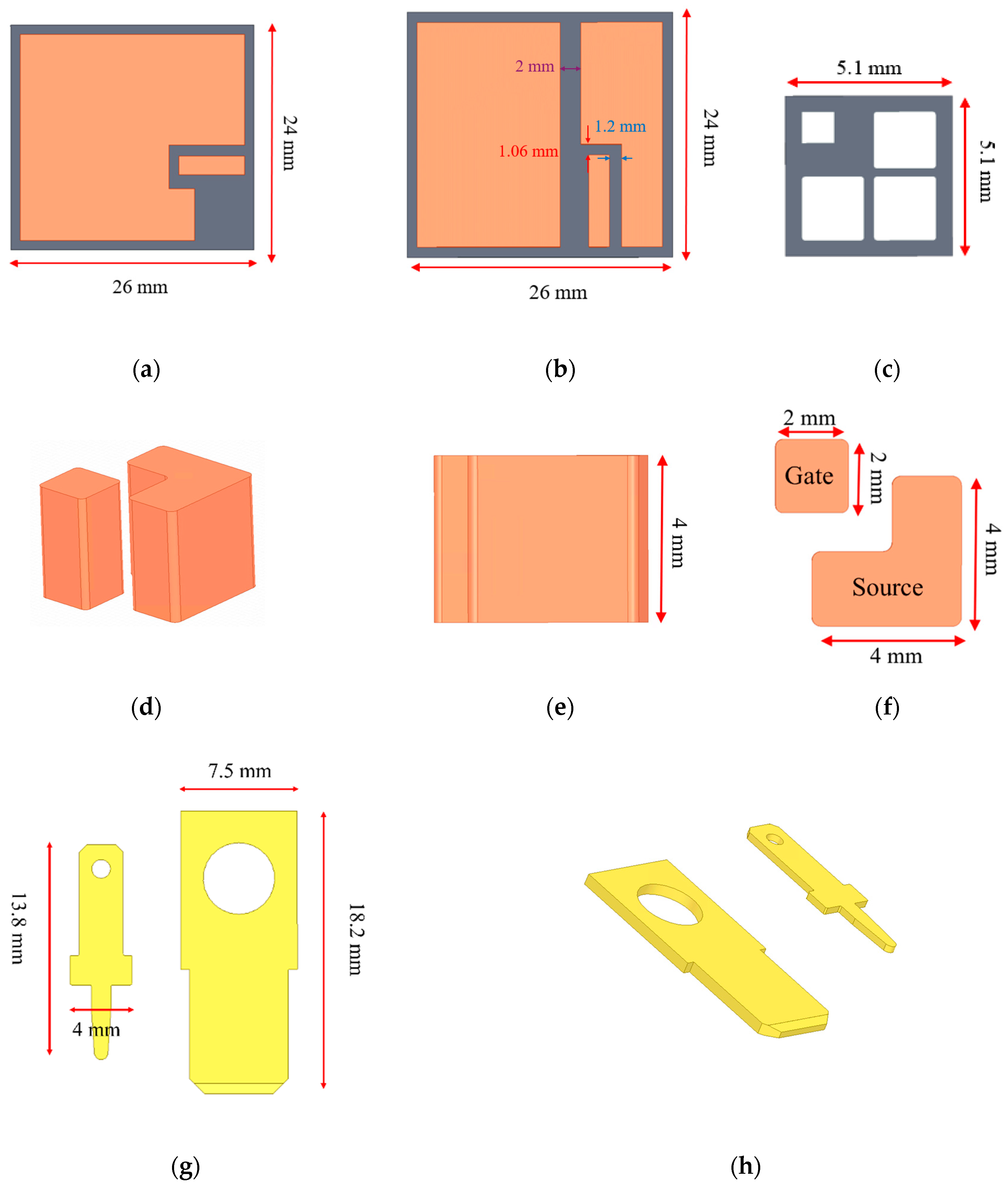
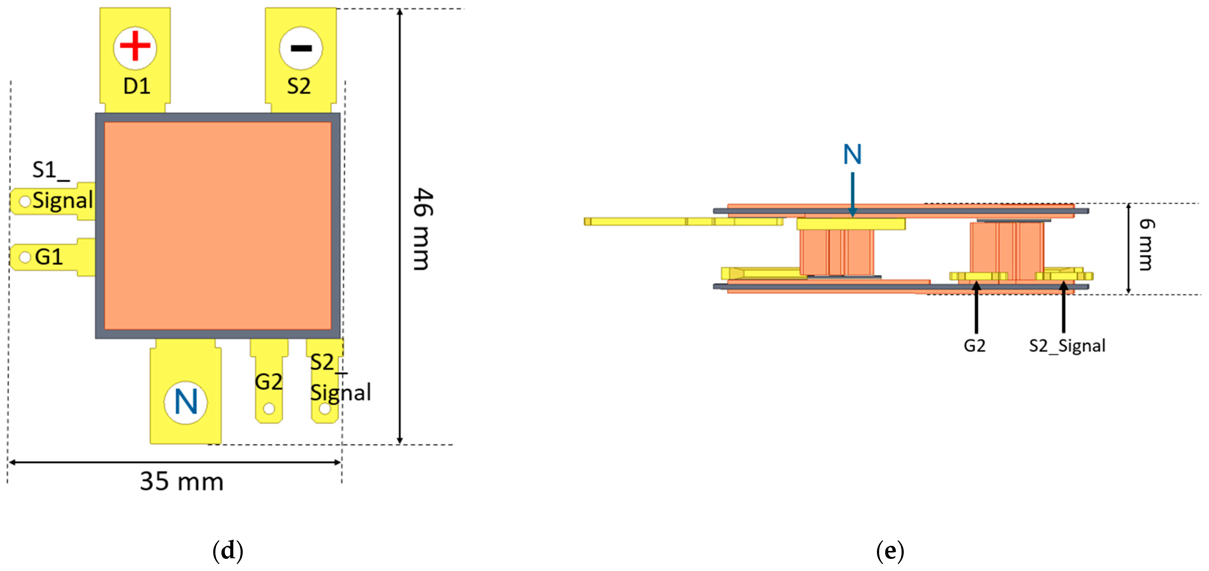
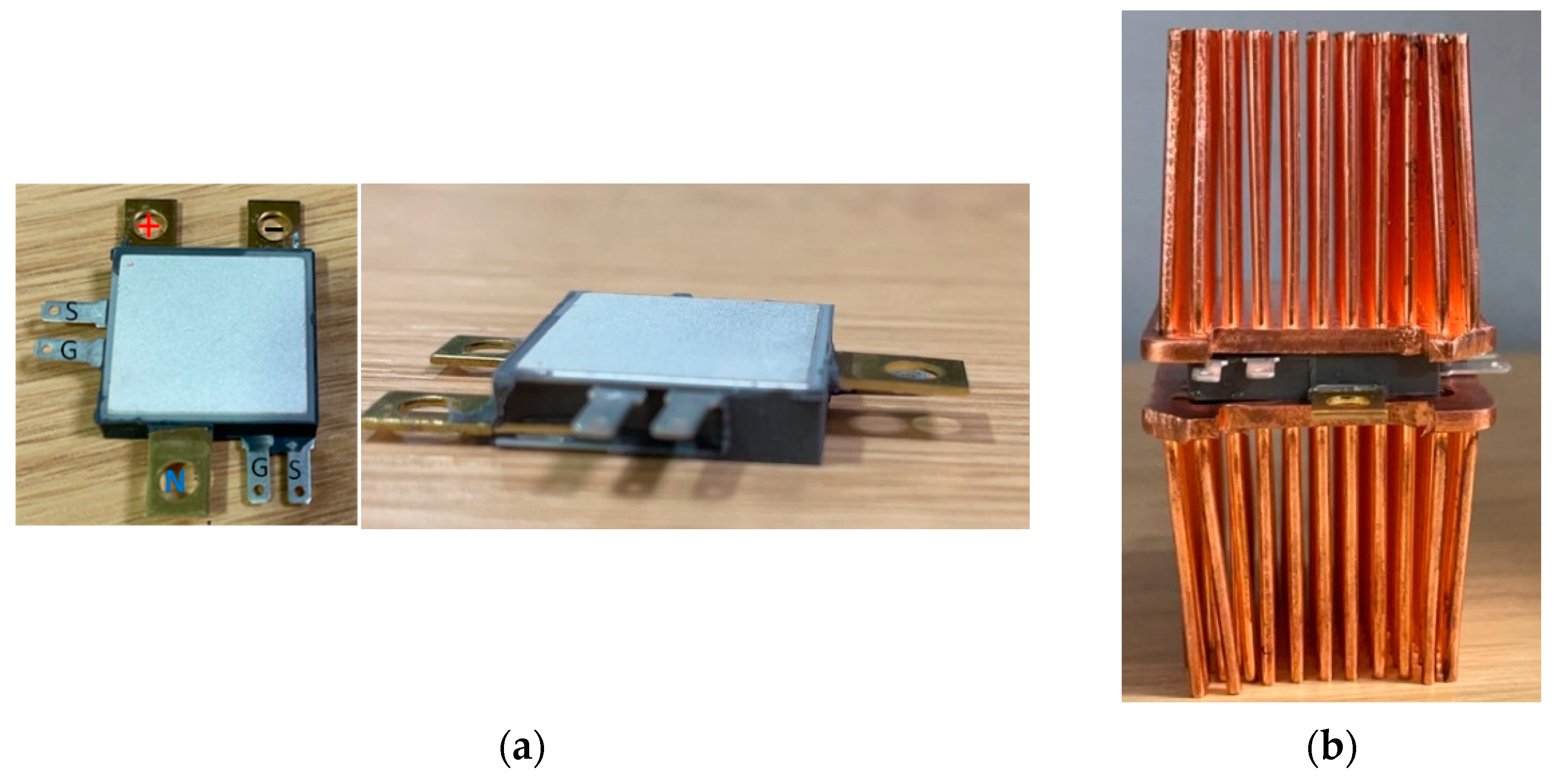
2.1. Layout of AMB Boards, Customised Copper Connectors, Bare Die, and Power and Signal Connectors

In contrast to the single-sided converter, this double-sided design incorporates two AMB substrates within the circuit, positioned to make a sandwich structure, with the chip in the middle (the filling). The AMB substrates, crafted by the authors, are illustrated in Figure 1a,b, featuring a layout-side copper thickness of 0.3 mm, a Si3N4 base thickness of 0.32 mm, and a backside copper thickness of 0.3 mm. When designing the layout of the DBC board, both the feasibility and design rules for AMB circuit are taken into consideration. Commonly used design rules are as follows:
  • Position the gate contact close to the die to minimise stray inductance;
  • Arrange the current flow from the die to the source contact in the opposite direction to the current flow from the drain to the die to reduce stray inductance;
  • Use Kelvin-source contacts for the gate signals to effectively minimise parasitic resistances and reduce false switching events.
The small copper blocks, as depicted in Figure 1d–f, are utilised in the design to establish connections between the two AMB substrates, thereby facilitating the interconnection between the upper and lower SiC devices within the half-bridge circuit. Research shows this kind of copper connector can significantly reduce the stray inductance compared with traditional wire bonds or copper clips [22]. In this study, the distance between the two substrates is designed to be 4 mm, primarily constrained by the assembly capabilities within the laboratory. This selection allows us to strike a balance between minimising stray inductance and addressing practical assembly considerations. It is noteworthy that while this value is subject to adjustment in accordance with specific application requirements, such adaptions may be facilitated by enhanced packaging tools. Figure 1c shows the bare die (SCT110N120G3D2AG) employed in this power module, and Figure 1g,h show the front and general view of the power and signal connector of the module. These two components are selected based on market availability.

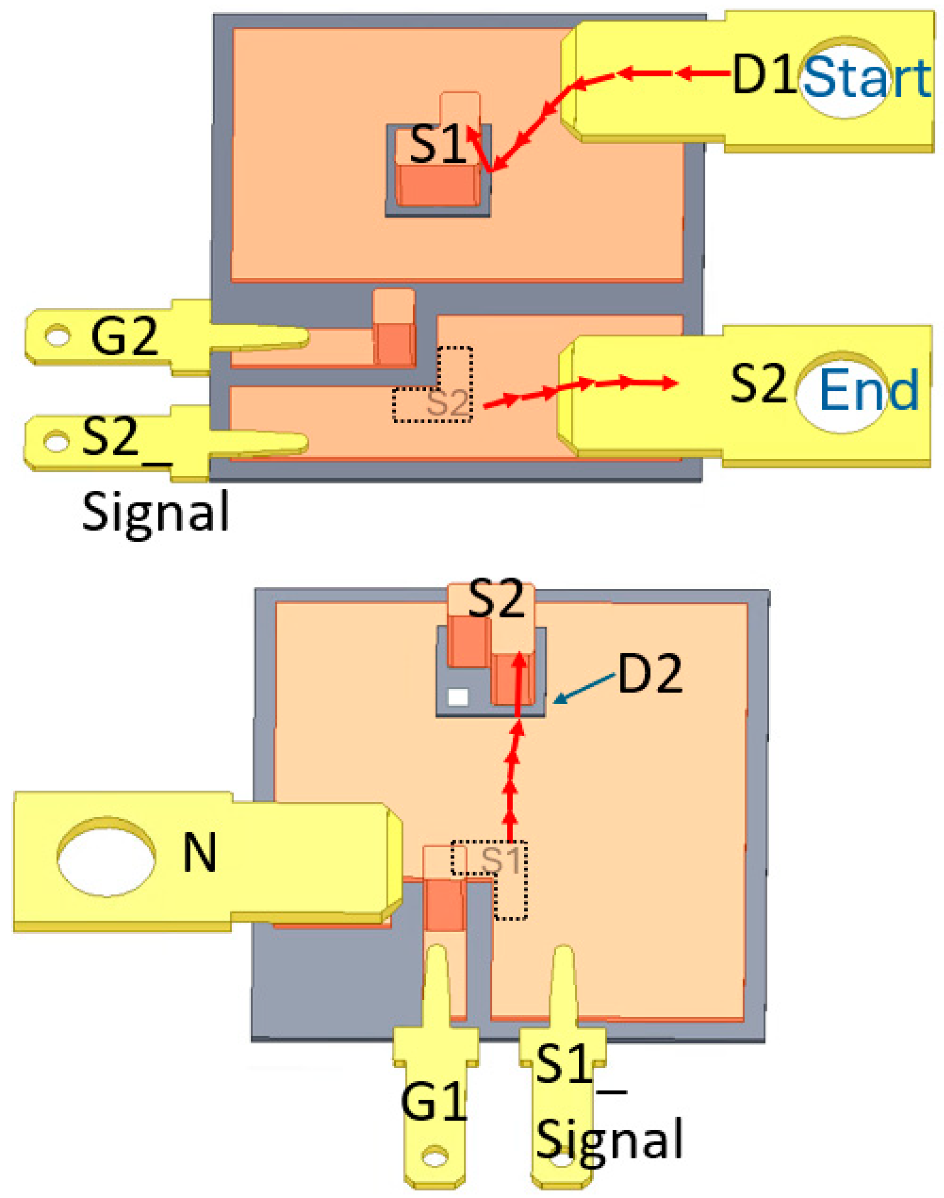
2.2. Assembling of the Double-Sided Half-Bridge Circuit

The actual assembly process of the double-sided half-bridge is depicted in detail in Section 4. Figure 2 below is used for the demonstration of the construction of the power module, rather than displaying the actual packaging process. Figure 2a illustrates the first step, where MOSFET dies both for upper legs and lower legs are attached to the AMB substrate. In the second step, the customised copper blocks are sintered on to the source pads of the MOSFET dies, as shown in Figure 2b. In the third step, signal and power connectors, as well as the customised gate copper blocks, are attached onto both substrates, as depicted in Figure 2c. In the final step, the substrate on the right-hand side of Figure 2c is flipped and aligned with the substrate on the left. The final assembly can be seen in Figure 2d,e.

2.3. Insulation Consideration for the Proposed Power Module

When designing the packaging structure of a high-power module, insulation must always be considered. The proposed power module is intended for 800 V EV applications, and according to IEC 62368, the minimum reinforced insulation for 800 V under Pollution Degree 1 (QSIL 550 encapsulation) is 0.5 mm. For example, as shown in Figure 1b, the minimum distance between the signal and power path (gate to source) is designed to be 1.06 mm, while the distance between power paths (drain to source) is set to 2 mm to provide additional protection. The spacing between the upper and lower AMB boards depends on the height of the copper block, as illustrated in Figure 1e. As already mentioned in Section 2.1, a 4 mm spacing was chosen due to the limited assembly capabilities available in our laboratory; however, this can be reduced to 2 mm in future iterations.

3. Ansys Q3D and Icepak Simulation of the Double-Sided Half-Bridge Circuit

In this section, Ansys Q3D is utilised to extract parasitic parameters of the half-bridge circuit depicted in Figure 2 or Figure 3. Meanwhile, Icepak 3D Finite Volume Method (FVM) models are employed to simulate the steady-state temperature of both the double-sided half-bridge circuit and the single-sided counterpart [22]. This demonstrates the advantages associated with double-sided cooling.

3.1. Simulation of the Positive to Negative Stray Inductance

Based on the research findings in [22], the impact of silver coating, solder, and silver paste on the surface on the stray inductance of the circuit is deemed insignificant and hence will be disregarded in this paper.
Figure 4 presents the results of Ansys Q3D simulations illustrating how the stray inductance varies with frequency. The inductance measurement path can be seen in Figure 3. In Figure 3, the dotted regions (S1 and S2) indicate the locations of electrical connections for S1 and S2 pillars. Throughout the simulation, the SiC MOSFETs were temporarily represented as copper blocks. The stray inductance of the double-sided module reached approximately 4.7 nH at 5 MHz.
A stray inductance measurement method was previously described in [22], verifying the accuracy of the simulation method. In this paper, the stray inductance simulation method is identical to that in [22], making the simulation result of 4.7 nH a reliable and accurate value. It should be noted that the proposed module in this paper features a scalable design with a single die in both the upper and lower legs. When expanded to, for example, two or five dies in parallel, the stray inductance can be reduced to as low as 2.4 nH and 0.9 nH, respectively, demonstrating that the design can be considered an ultra-low-stray-inductance power module.
A comparison between the proposed power module and two commercial modules is shown in Table 1. Since high-power double-sided cooling modules with SiC are not widely available in the market, one of the latest single-sided half-bridge modules with SiC and one double-sided half-bridge module with an Insulated Gate Bipolar Transistor (IGBT) were selected for comparison. These results highlight the benefits of the wire-bonding-free design implemented in the power module.

3.2. Comparison Between the Thermal Performance of the Single-Side Cooling Design and Double-Sided Cooling Design

To highlight the thermal advantages of the double-sided cooling, this section presents a comparative analysis of the thermal performance between the single-sided cooling module detailed in [22] and the double-sided cooling module, under two different conditions. They are (1) general operating condition and (2) extreme operating condition. The SiC bare die, power, voltage, current rating of the modules and the simulation parameters for both configurations are set to be identical, as listed in Table 2.

3.2.1. General Operating Condition

The total losses estimated in Table 2 include the conduction losses and switching losses. According to the datasheet of the bare die, the rated drain current ID at 100 °C case temperature is 79 A. A maximum output current of 70 A, which equates to a Root Mean Square (RMS) current of 50 A, is considered as the case for analysis. The on-state resistance is 35 mΩ at high junction temperature, so the conduction losses can be calculated as
(50 A)2 × 35 mΩ = 87.5 W
As for the switching losses, the Turn-ON and Turn-OFF losses of the proposed module are 2.7 mJ and 4.2 mJ, respectively, under the conditions VDD = 400 V, VGS = 17 V and ID = 50 A. Assuming the switching frequency is 10 kHz, the average power loss can be estimated as
(2.7 + 4.2) mJ × 10 kHz = 69 W
The total losses are obtained by adding up the switching loss and conduction loss, resulting in 156.5 W.
Figure 5 illustrates the simulation result obtained by Ansys Icepak for both designs under general identical power loss conditions, which is 156.5 W. The junction temperature of the dies in the single-sided cooling setup reaches around 138 °C, whereas in the double-sided cooling configuration, it is approximately 108 °C. As expected, the double-sided cooling module dissipates heat more effectively, reducing the junction temperature by nearly 30 °C. Despite the pin-fin heatsink surface area of the single-sided model being about 2.8 times larger than that of the double-sided model (one plate), the double-sided design proves more efficient.

3.2.2. Extreme Operating Condition

Figure 6 shows the thermal performance of both designs under extreme conditions calculated in (3) for conduction losses and (4) for switching losses. It assumes continuous operation at peak current, with a high switching frequency of 16 kHz, resulting in 323.5 W total losses. Under typical operating conditions, the junction temperatures of both devices are expected to be lower than those presented in Figure 6.
(70 A)2 × 35 mΩ = 171.5 W
(3.7 + 5.8) mJ × 16 kHz = 152 W
From Figure 6, it can be seen that the junction temperature (Tj) of the single-sided design reaches 238 °C, exceeding the operating range of the power die (−55 °C to 200 °C). In contrast, Tj of the double-sided design is around 199 °C, which is 39 °C lower than the single-sided design. These simulation results demonstrate that the double-sided design can operate under extreme power loss conditions. Importantly, such events are rare in real-world operation, occurring only a few times over the entire lifetime of the module. It is widely recognised in the industry that short-duration operation above the standard maximum junction temperature is acceptable under certain conditions. Top manufacturers such as Infineon, onsemi, and ROHM explicitly guarantee safe operation between 175 °C and 200 °C for limited time durations, typically ranging from ten hours up to hundreds of hours, without compromising device reliability. These allowances are made to handle infrequent but harsh transients.
Moreover, the new generation of SiC modules such as STMicroelectronics’ TPAK series is already rated for continuous operation at Tj = 200 °C, reflecting the industry’s shift toward higher thermal robustness. Therefore, although the simulated 199 °C Tj nearly reaches the 200 °C threshold, it occurs only during rare, short-lived events and is well within the thermal capability envelope defined by major SiC device manufacturers, ensuring system reliability is not compromised.

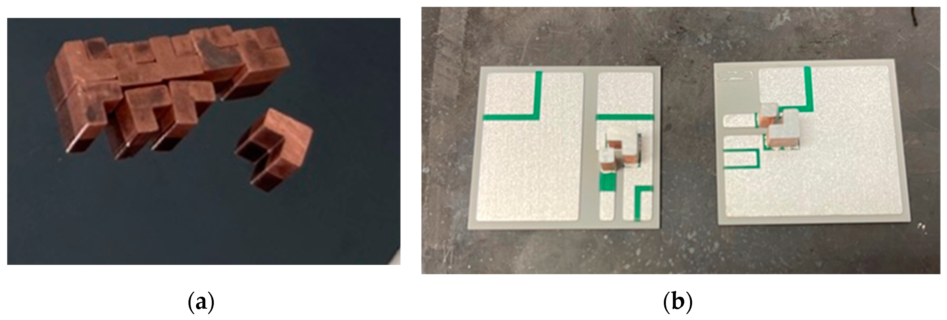
4. Packaged Module of the Double-Sided Half-Bridge Circuit

The packaging process for a double-sided module is more complex compared to that of a single-sided module. Firstly, while the packaging of a single-sided module typically involves a single reflowing process, assembling a double-sided module may require multiple reflowing procedures under university laboratory conditions. Secondly, constructing an encapsulation wall is considerably simpler for a single-sided package, whereas the encapsulation material in a double-sided package may endure higher temperatures due to injection before heatsink soldering. Lastly, each layer of the double-sided module must remain horizontal during the reflowing process to prevent any disconnections. The entire process for the packaging of the double-sided half-bridge can be divided into four steps.
First step: Customised small copper block coating: Given that both sides of the small copper blocks necessitate attachment with silver material, silver coating is imperative prior to assembly. Both the original and silver-coated copper blocks, as well as the AMB substrates with silver coating, can be observed in Figure 7. The thickness of the silver layer for both copper blocks and substrates is set at 0.5 µm.
Second step: Assembly with customised jigs: All SiC bare dies and small copper blocks must be sintered at specific positions on the DBC boards. Consequently, jigs specifically designed for this purpose are indispensable during the reflowing procedures. The sintering/soldering procedures can be divided into three steps. Firstly, aided by jigs depicted in Figure 8a, one side of all the small copper blocks and the SiC dies are sintered on two AMB substrates. Secondly, the two substrates are positioned face to face, and the other side of all the small blocks are sintered on the opposing AMB substrate as depicted in Figure 8b. The nanosilver paste by NanoTach (headquartered in Katy, TX, USA). was used for the die attachment. It can be sintered at temperatures below 260 °C using a pressureless process. Once the bond is formed, it will not melt unless temperatures reach 960 °C. Lastly, all the power and signal connectors are soldered onto both AMB substrates simultaneously. Notably, if soldering the connectors on the top substrate, supports are required to hold the connectors in place. In this study, polyimide electrical tape is utilised for this purpose.
Third step: Encapsulation with customised jigs: Unlike most single-sided designs, which typically entail straightforward construction of encapsulation walls, this double-sided design resembles a square sandwich, necessitating walls on at least three sides. Customised jigs printed by a 3D printer are applied to the module post-assembly to provide walls for silicone gel filling. The silicone encapsulant used in this module is QSIL 550 (CHT Germany GmbH, headquartered in Tübingen, Germany), boasting a wide operating temperature range (−115 °C to 300 °C), ensuring its suitability for the reflowing oven during the final pin-fin heatsink soldering step (179 °C solder paste) as shown in Figure 9b.
Fourth step: With and without heatsink: The packaged half-bridge is showcased in Figure 9, both without (a) and with (b) a pin-fin heatsink. It is worth noting that the pin-fin heatsink utilised in this study is not customised or optimised but is based on availability in the market. Designing a pin-fin heatsink specifically for this model could potentially involve reducing the length of the pins and enhancing their stiffness. In fact, a pin-fin with a length ranging within 3~5 mm is sufficient for efficient heat dissipation.

5. Electrical Test of the Packaged Double-Sided Half-Bridge Converter

In this paper, the primary focus is on advanced packaging strategies for high-power SiC modules. Electrical tests were conducted under low-power conditions to evaluate the fundamental characteristics of the design. High-power testing will be considered in future work using a comprehensive test setup, such as a liquid-immersion cooling system, to assess performance under full operating conditions.

5.1. Double Pulse Test

A standard double pulse test at low power was conducted in the laboratory, as depicted in the circuit diagram shown in Figure 10a. The Device Under Test (DUT) was designated as the lower bridge switch, with the load inductor L connected between the VDC+ connector and the AC connector. The test outcomes for a DC voltage of 300 V and current of 10 A are presented herein. The waveforms depicting the Turn OFF of the first pulse and the Turn ON of the second pulse from the oscilloscope are showcased in Figure 10b. Additionally, a zoomed-in view of each switching transient is provided in Figure 10c and Figure 10d, respectively. The observed rise and fall times are approximately 200 ns, with a voltage overshoot of only 50 V during Turn OFF. The gate driver used in the test has not been optimised; therefore, the transient performance of the power module can be further improved by utilising an optimised gate driver design.

5.2. Inductive Load Test

The double pulse tests have demonstrated the capability of the fabricated module to fulfil its intended function. For additional validation, an inductive load test was conducted. The test circuit, as depicted in Figure 11a, featured a zoomed-in view of the waveform of two fundamental cycles, showcased in Figure 11b. The gate signal was open-loop controlled to produce a sinusoidal wave of the fundamental frequency of 50 Hz and a switching frequency of 10 kHz. The DC voltage was fixed at 250 V, and the modulation index was set at 0.9. The current amplitude was approximately 15 A.

6. Conclusions

This study focuses on designing, developing, and testing an innovative wire-bondless double-sided cooling half-bridge power module. In comparison with single-sided cooling, this design exhibits significantly improved thermal performance under identical power conditions. The junction temperature reduced by about 30 °C and 39 °C under normal and extreme operating conditions, and the double-sided cooling helped to control the maximum temperature (199 °C) below the limitation of the die (200 °C) even under the very extreme operating situation. Additionally, the wire-bondless design contributes to enhancing operational lifespan and reducing stray inductance. In the design with a single die for each leg, the stray inductance is as low as 4.7 nH. As it is a scalable design, stray inductance for packaging with two and five dies in parallel is estimated and compared with similar power modules. The estimated stray inductance for the design with five parallel dies is as low as 0.9 nH, which is the ultra-low-stray-inductance design.
Cutting-edge silver sintering and Si3N4 technology are integrated into the design to enhance the thermal conductivity, reliability, mechanical strength, and thermal stability of the packaged module. The module underwent electrical testing, including double-pulse and inductive load tests, to validate its electrical characteristics. Future endeavours will explore the design with multi-dies in parallel and further advancements in double-sided packaging technology to optimise the packaging procedure. Additionally, future work can include further physical and electrical testing, such as thermal shock tests, power loss measurements, power cycling tests, high-power operating evaluations and closed-loop testing.

Author Contributions

Conceptualization, X.R., R.W. and P.M.; methodology, X.R., R.W. and P.M.; software, X.R. and R.W.; validation, X.R., R.W. and P.M.; investigation, X.R.; resources, X.R., R.W. and P.M.; data curation, X.R. and R.W.; writing—original draft preparation, X.R. and R.W.; writing—review and editing, X.R. and P.M.; visualisation, X.R., R.W. and P.M.; supervision, P.M.; project administration, P.M.; funding acquisition, P.M. All authors have read and agreed to the published version of the manuscript.

Funding

This research was funded by the Engineering and Physical Sciences Research Council (EPSRC 56835) Prosperity Partnership project between the University of Warwick and Jaguar Land Rover. It aims at the research of fundamental engineering and technical problems to enable Jaguar Land Rover to bring cutting-edge developments to improve its products and processes for long-term technological advantage. The focus of the project is on four research areas: Battery Technology, Power Electronics, Electric Machine Design and Propulsion Systems.

Data Availability Statement

The original contributions presented in the study are included in the article; further inquiries can be directed to the corresponding authors.

Conflicts of Interest

The author Ruizhu Wu was employed by the company Chongqing Seres Phoenix Intelligent Innovation Technology Co., Ltd. The remaining authors declare that the research was conducted in the absence of any commercial or financial relationships that could be construed as a potential conflict of interest.

References

  1. Tang, G.; Chai, T.C.; Zhang, X. Thermal Optimization and Characterization of Sic-Based High Power Electronics Packages with Advanced Thermal Design. IEEE Trans. Compon. Packag. Manuf. Technol. 2019, 9, 854–863. [Google Scholar] [CrossRef]
  2. Zhang, Y.; Chen, G.; Hu, Y.; Gong, C.; Wang, Y. Cascaded Multilevel Inverter Based Power and Signal Multiplex Transmission for Electric Vehicles. CES Trans. Electr. Mach. Syst. 2020, 4, 123–129. [Google Scholar] [CrossRef]
  3. Reis, F.E.U.; Torrico-Bascope, R.P.; Tofoli, F.L.; Santos Bezerra, L.D. Bidirectional Three-Level Stacked Neutral-Point-Clamped Converter for Electric Vehicle Charging Stations. IEEE Access 2020, 8, 37565–37577. [Google Scholar] [CrossRef]
  4. Luciano, F.S.A.; Ruan, C.M.G.; Pierre, L.; Raoni, D.A.P.; Jeannin, P.-O.; Luciano, B.A.; Rocha, F.V. SIC Power Devices in Power Electronics: An Overview. In Proceedings of the 2017 Brazilian Power Electronics Conference (COBEP), Juiz de Fora, Brazil, 15 January 2017; pp. 1–8. [Google Scholar]
  5. Yu, S.; Wang, J.; Zhang, X.; Liu, Y.; Jiang, N.; Wang, W. The Potential Impact of Using Traction Inverters with SiC MOSFETs for Electric Buses. IEEE Access 2021, 9, 51561–51572. [Google Scholar] [CrossRef]
  6. Matsuoka, T.; Ohki, A.; Ohno, T.; Kawaguchi, Y. Comparison of GaN- and ZnSe-Based Materials for Light Emitters. J. Cryst. Growth 1994, 138, 727–736. [Google Scholar] [CrossRef]
  7. Shur, M. Wide Band Gap Semiconductor Technology: State-of-the-Art. Solid State Electron. 2019, 155, 65–75. [Google Scholar] [CrossRef]
  8. Shivakumar, S.; Yoon, J.; Sirkar, T. Gallium Nitride: A Strategic Opportunity for the Semiconductor Industry. Available online: https://www.csis.org/analysis/gallium-nitride-strategic-opportunity-semiconductor-industry?utm_source=chatgpt.com (accessed on 25 March 2025).
  9. Ke, H.; Mehrotra, U.; Hopkins, D.C. 3-D Prismatic Packaging Methodologies for Wide Band Gap Power Electronics Modules. IEEE Trans. Power Electron. 2021, 36, 13057–13066. [Google Scholar] [CrossRef]
  10. Paret, P.; Cousineau, J.E.; Narumanchi, S.; Lu, G.Q.; Ngo, K. Thermal and Mechanical Design of a High-Voltage Power Electronics Package. In Proceedings of the 2021 IEEE Applied Power Electronics Conference and Exposition (APEC), Phoenix, AZ, USA, 14–17 June 2021; pp. 50–54. [Google Scholar]
  11. Fernandes, B.G. Review of Power Electronics Packaging and the Use of Copper as Heat Sink; Torrey Hills Technologies, LLC: San Diego, CA, USA, 2013. [Google Scholar]
  12. Le Henaff, F.R.; Azzopardi, S.; Theolier, L.; Deletage, J.-Y. Silver Sintering Wire-Bonding Less Power Module for High Temperature Applications. In Proceedings of the Symposium de Génie Électrique 2014, Cachan, France, 8–10 July 2014. [Google Scholar]
  13. Gao, S.; Yang, Z.; Tan, Y.; Li, X.; Chen, X.; Sun, Z.; Lu, G.Q. Bonding of Large Substrates by Silver Sintering and Characterization of the Interface Thermal Resistance. IEEE Trans. Ind. Appl. 2019, 55, 1828–1834. [Google Scholar] [CrossRef]
  14. Wang, M.; Mei, Y.; Li, X.; Burgos, R.; Boroyevich, D.; Lu, G.Q. Pressureless Silver Sintering on Nickel for Power Module Packaging. IEEE Trans. Power Electron. 2019, 34, 7121–7125. [Google Scholar] [CrossRef]
  15. Yan, H.; Liang, P.; Mei, Y.; Feng, Z. Brief Review of Silver Sinter-Bonding Processing for Packaging High-Temperature Power Devices. Chin. J. Electr. Eng. 2020, 6, 25–34. [Google Scholar] [CrossRef]
  16. Chen, H.; Hossain, M.M.; Gonzalez Castillo, D.; Li, X.; Wallace, A.; Chen, Y.; Mantooth, H.A. Design and Optimization of SiC MOSFET Wire Bondless Power Modules. In Proceedings of the 2020 IEEE 9th International Power Electronics and Motion Control Conference, IPEMC 2020 ECCE Asia, Nanjing, China, 29 November–2 December 2020; pp. 725–728. [Google Scholar]
  17. Seal, S.; Wallace, A.K.; Dearien, A.M.; Farnell, C.; Mantooth, H.A. A Wire Bondless SiC Switching Cell with a Vertically Integrated Gate Driver. IEEE Trans. Power Electron. 2020, 35, 9692–9701. [Google Scholar] [CrossRef]
  18. Chen, Y.; Lei, G.; Lu, G.Q.; Mei, Y.H. High-Temperature Characterizations of a Half-Bridge Wire-Bondless SiC MOSFET Module. IEEE J. Electron Devices Soc. 2021, 9, 966–971. [Google Scholar] [CrossRef]
  19. Zhang, H.; Ang, S.S.; Mantooth, H.A.; Krishnamurthy, S. A High Temperature, Double-Sided Cooling SiC Power Electronics Module. In Proceedings of the 2013 IEEE Energy Conversion Congress and Exposition, Denver, CO, USA, 28 October 2013; pp. 2877–2883. [Google Scholar]
  20. Charboneau, B.C.; Wang, F.; Van Wyk, J.D.; Boroyevich, D.; Liang, Z.; Scott, E.P.; Tipton, C.W. Double-Sided Liquid Cooling for Power Semiconductor Devices Using Embedded Power Packaging. In Proceedings of the Fourtieth IAS Annual Meeting, Conference Record of the 2005 Industry Applications Conference, Hong Kong, China, 2–6 October 2005; pp. 1138–1143. [Google Scholar]
  21. Wang, M.; Mei, Y.; Liu, W.; Xie, Y.; Fu, S.; Li, X.; Lu, G.Q. Reliability Improvement of a Double-Sided IGBT Module by Lowering Stress Gradient Using Molybdenum Buffers. IEEE J. Emerg. Sel. Top. Power Electron. 2019, 7, 1637–1648. [Google Scholar] [CrossRef]
  22. Rong, X.; Wu, R.; Mawby, P. Simulation and Testing of a Newly Designed Half Bridge Module with Silicon Carbide MOSFET. In Proceedings of the 12th International Conference on Power Electronics, Machines and Drive, Brussels, Belgium, 23 October 2023; Volume 2023, pp. 462–469. [Google Scholar]
  23. Marcinkowski, J. Dual-Sided Cooling of Power Semiconductor Modules. In Proceedings of the International Exhibition and Conference for Power Electronics, Intelligent Motion, Renewable Energy and Energy Management, Nuremberg, Germany, 20 May 2014; pp. 1–7. [Google Scholar]
  24. Liu, M.; Coppola, A.; Alvi, M.; Anwar, M. Comprehensive Review and State of Development of Double-Sided Cooled Package Technology for Automotive Power Modules. IEEE Open J. Power Electron. 2022, 3, 271–289. [Google Scholar] [CrossRef]
  25. Li, Y.; Zhu, S.; Ma, Y.; Wang, Y.; Jiao, M.; Wu, C.; Zhao, Z.; Yu, J. Highly Integrated Power Unit Based on Double Side Cooling Module. In Proceedings of the International Exhibition and Conference for Power Electronics, Intelligent Motion, Renewable Energy and Energy Management, Nuremberg, Germany, 16 May 2017; pp. 1–6. [Google Scholar]
  26. Brian, P.; Srikanth, K.; Aicha, E.; Fred, B. Evaluation of Direct Bond Aluminum Susbtrates for Power Electronic Applications in Extreme Environments. In Proceedings of the IMAPS/ACerS 8th International CICMT Conference and Exhibition, Erfurt, Germany, 16 April 2012. [Google Scholar]
  27. Wang, X. Silicon Nitride and Electric Vehicles. In Proceedings of the International Exhibition and Conference for Power Electronics, Intelligent Motion, Renewable Energy and Energy Management, Shenzhen, China, 3–7 May 2021; pp. 1–4. [Google Scholar]
  28. Wolfspeed. CAB400M12XM3 1200 V SiC Power Module Data Sheet; Wolfspeed: Durham, UK, 2024. [Google Scholar]
  29. Infineon. FF400R07A01E3_S6 DoubleSideCooledModule; Infineon: Munich, Germany, 2020. [Google Scholar]
  30. Zeng, Z.; Ou, K.; Wang, L.; Yu, Y. Reliability-Oriented Automated Design of Double-Sided Cooling Power Module: A Thermo-Mechanical-Coordinated and Multi-Objective-Oriented Optimization Methodology. IEEE Trans. Device Mater. Reliab. 2020, 20, 584–595. [Google Scholar] [CrossRef]
Figure 1. Design of the main parts for the assembly of the double-sided power module: (a) AMB substrate board 1 (top); (b) AMB substrate board 2 (bottom); (c) bare die; (d) general view of the customised copper connectors; (e) side view of the customised copper connectors; (f) top view of the customised copper connectors; (g) top view of the signal and power connector; (h) general view of the signal and power connectors.
Electronics 14 01520 g001
Figure 2. Assembly of the double-sided half-bridge circuit: (a) die attachment; (b) attachment of the customised copper block (source); (c) attachment of the customised copper block (gate), signal and power connectors; (d) top view of the final assembly; (e) side view of the final assembly.
Electronics 14 01520 g002aElectronics 14 01520 g002b
Figure 3. Positive to negative stray inductance path.
Electronics 14 01520 g003
Figure 4. Stray inductance of the circuit between positive and negative connector.
Electronics 14 01520 g004
Figure 5. Comparison of the thermal performance of single-sided cooling and double-sided cooling module under general operating condition: (a) thermal simulation of single-sided cooling; (b) thermal simulation of double-sided cooling.
Electronics 14 01520 g005
Figure 6. Comparison of the thermal performance of single-sided cooling and double-sided cooling module under extreme operating condition: (a) thermal simulation of single-sided cooling; (b) thermal simulation of double-sided cooling.
Electronics 14 01520 g006
Figure 7. Customised small copper block and AMB substrates: (a) original small copper blocks; (b) evaporated copper blocks and their position on AMB substrates.
Electronics 14 01520 g007
Figure 8. Alignment jig for assembly: (a) alignment jig for copper block and die—reflowing step 1 (silver sintering); (b) alignment jig for DBC boards—reflowing step 2 (silver sintering); (c) power and signal connector soldering—reflowing step 3 (soldering).
Electronics 14 01520 g008
Figure 9. Packaged half-bridge: (a) without pin-fin heatsink; (b) with pin-fin heatsink—heatsink based on market availability, not optimised.
Electronics 14 01520 g009
Figure 10. Double pulse test: (a) test circuit; (b) oscilloscope screenshot of the Turn OFF of the first pulse and the Turn ON of the second pulse; (c) Turn ON transient; (d) Turn OFF transient.
Electronics 14 01520 g010
Figure 11. Inductive load test: (a) experiment setup; (b) measured current.
Electronics 14 01520 g011
Table 1. Comparison of the proposed power module with commercial power modules [28,29,30].
Type of the Half-Bridge Power ModuleVoltage Rating (V)Cooling TypeDies in ParallelStray Inductance (nH)SiC or IGBT
Proposed Power
module
1200Double sided14.7
2.4 (2 die in parallel)
0.9 (5 die in parallel)
SiC
Infineon FF400R07A01E3_S6700Double-sided215IGBT
Wolfspeed CAB400M12XM31200Single-Sided56.7SiC
Table 2. Thermal simulation parameters of single-sided and double-sided cooling SiC power modules.
AMB Board Size
(L × W × H) (mm)
Heat Sink Size Including Pin Fin
(L × W × H) (mm)
Cooling Water Flowing Speed and TemperatureTotal Loss Estimated
(W)
Single-Sided Cooling39 × 26 × 0.9245 × 33 × 130.5 m/s
20 °C initial temperature
156.5 (General)
323.5 (Extreme)
Double-Sided Cooling26 × 24 × 0.92
(×2)
24 × 22 × 13
(×2)
Disclaimer/Publisher’s Note: The statements, opinions and data contained in all publications are solely those of the individual author(s) and contributor(s) and not of MDPI and/or the editor(s). MDPI and/or the editor(s) disclaim responsibility for any injury to people or property resulting from any ideas, methods, instructions or products referred to in the content.

