1. Introduction
Omnidirectional antennas, which can transmit and receive electromagnetic waves uniformly in all directions, are crucial in wireless communication systems such as WLAN, Bluetooth [
1,
2,
3], and other fields of MIMO [
4,
5,
6]. Traditional omnidirectional designs primarily using monopole antennas have high-profile structures that impede integration with low-profile systems. While recent advancements leverage high-order modes in circular or ring-shaped structures to achieve omnidirectionality, these designs face limitations in gain performance.
For instance, Economou designed an omnidirectional antenna with a circular structure. The antenna, with the TM
01 mode and surface current, presents a symmetrical distribution and achieves an omnidirectional pattern similar to that of the monopole antenna [
7]. Al-Zoubi designed an antenna with a center-fed circular ring structure that allows the antenna to operate in a high-order mode and realize an omnidirectional pattern. At a working frequency of 5.8 GHz, the antenna’s gain is 5.7 dBi [
8].
Yunliang designed several omnidirectional antennas, mainly by etching slots in the antenna structure and loading pin probes such that the antenna operates in the TM
01 and TM
20 modes to achieve an omnidirectional pattern, resulting in an antenna gain of 6 dBi at an operating frequency of 2.45 GHz [
9,
10].
Xiaohan Zhai proposed a broadband omnidirectional antenna based on the TM
01, TM
02, and TM
03 modes, realizing low-profile vertical polarization characteristics [
11]. Similarly, Oh. J designed a broadband vertically polarized omnidirectional antenna by utilizing the coupling effect of parasitic structures [
12]. Dong designed a low-profile vertically polarized omnidirectional antenna using the TM
01 and TM
02 modes of a microstrip antenna, achieving a gain of 2–5 dBi within an operating bandwidth of 1.7–2.79 GHz [
13].
Despite these efforts, all the aforementioned omnidirectional antennas achieve omnidirectional characteristics through the high-order mode of the antenna; however, the gain values of the antennas are not very high. Array-based approaches have been explored to enhance gain, but they introduce impractical size constraints [
14,
15,
16,
17,
18,
19,
20]. For example, Sun’s 2 × 2 bent-dipole array [
14,
15] and Yu’s dipole-parasitic unit array [
16] achieved omnidirectionality with gains of 2.4 dBi, yet their large footprints limit applicability in compact systems [
17].
Characteristic mode theory (CMT) has emerged as a powerful tool for effectively analyzing the different working modes of antennas and has been widely used in the design process of broadband, circularly polarized, and omnidirectional antennas [
21,
22,
23,
24]. Yang [
21] applied CMT to design a metamaterial-based antenna with a 16.6% operating bandwidth, while Shuai [
22] utilized CMT to achieve broadband omnidirectionality in a dipole array. However, these works did not address the dual challenges of high gain, low profile, and minimal pattern ripple simultaneously.
In this study, we propose two novel low-profile, high-gain omnidirectional antennas operating at 2.45 GHz. Antenna I employs a conventional microstrip patch structure operating in the high-order TM22 mode, while Antenna II integrates four metal probes to excite a quasi-TM11 mode. Using CMT, we analyzed the far-field radiation patterns and surface current distributions of both designs, ensuring symmetric excitation and low pattern ripple. A 1:4 power divider was designed to enable equal amplitude in-phase feeding, and both antennas were experimentally validated.
2. Design Process of Antenna Unit Structure
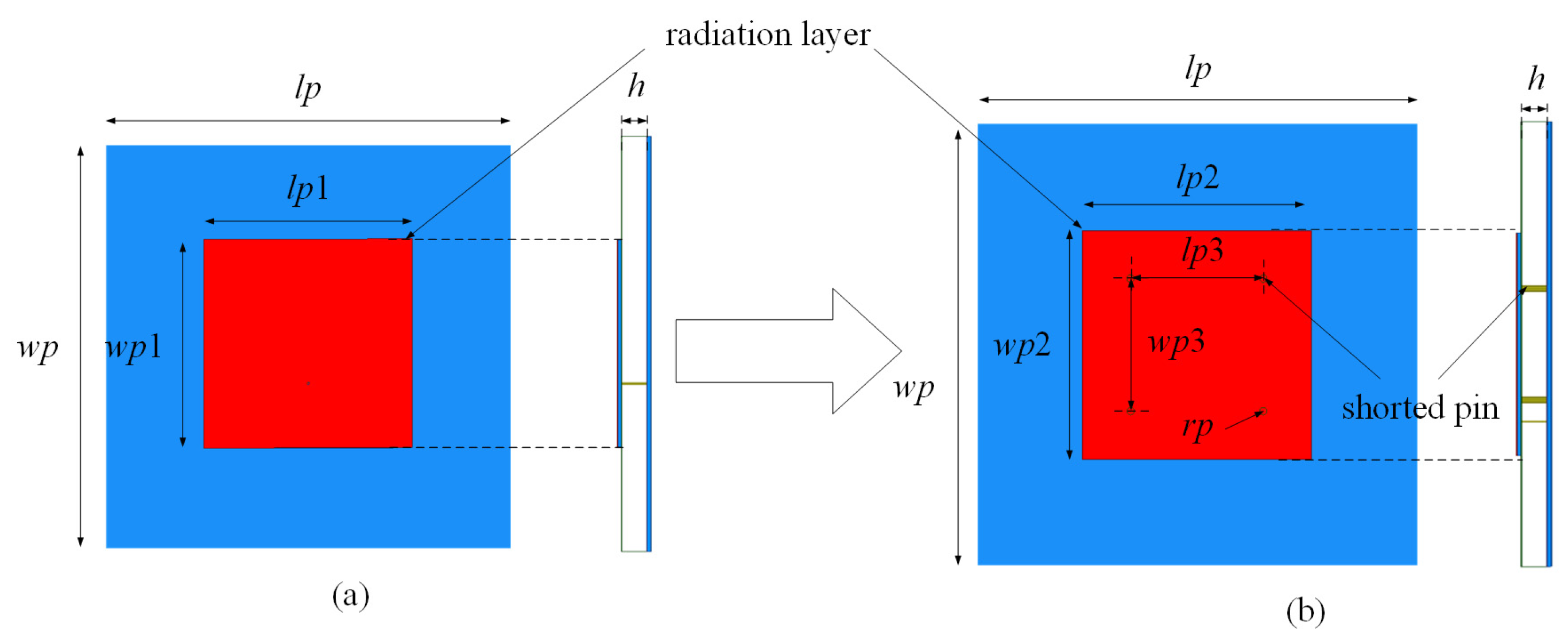
Figure 1 depicts the evolution of the antenna structure designed in this study.
Figure 1a illustrates a conventional microstrip patch antenna, while
Figure 1b shows a pin-loaded microstrip antenna structure. Previous studies have demonstrated that shorted pin-loaded microstrip antennas can achieve higher gain values compared to conventional microstrip antennas of the same size [
25,
26,
27,
28]. To realize high-gain omnidirectional radiation characteristics, a pin-loaded microstrip antenna structure was developed in this work.
The conventional microstrip antenna and the pin-loaded microstrip antenna have the same dielectric substrate and size. The dimensions of the antennas are as follows: lp = 104.4 mm, wp = 104.4 mm, lp1 = 52.2 mm, wp1 = 52.2 mm, lp2 = 62 mm, wp2 = 62 mm, lp3 = 36 mm, wp3 = 36 mm, rp = 1 mm, h = 3 mm.
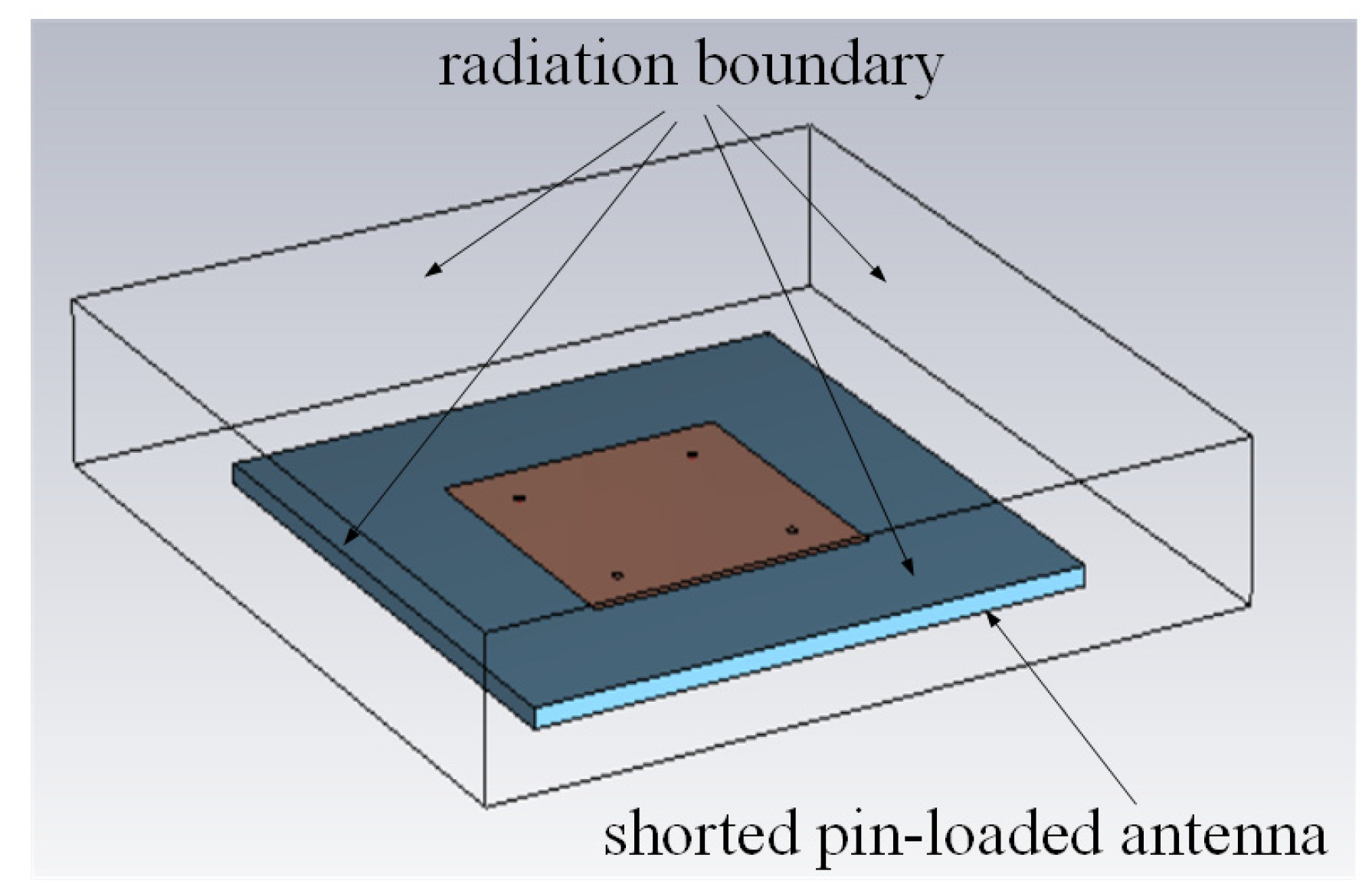
We employed the characteristic mode analysis (CMA) tool in the CST electromagnetic simulation software [
29] to investigate the radiation patterns and mode distributions of the antennas. The structure of the antenna in the electromagnetic simulation software CST is shown in
Figure 2. The area around the antenna was set as the radiation boundary condition, and the antenna dielectric layer was set as a lossless substrate material.
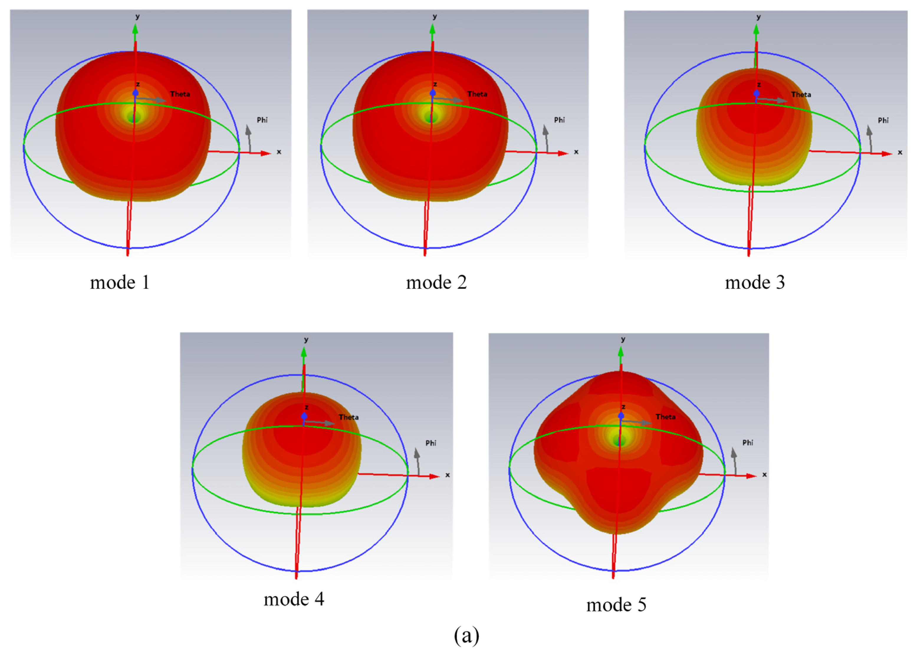
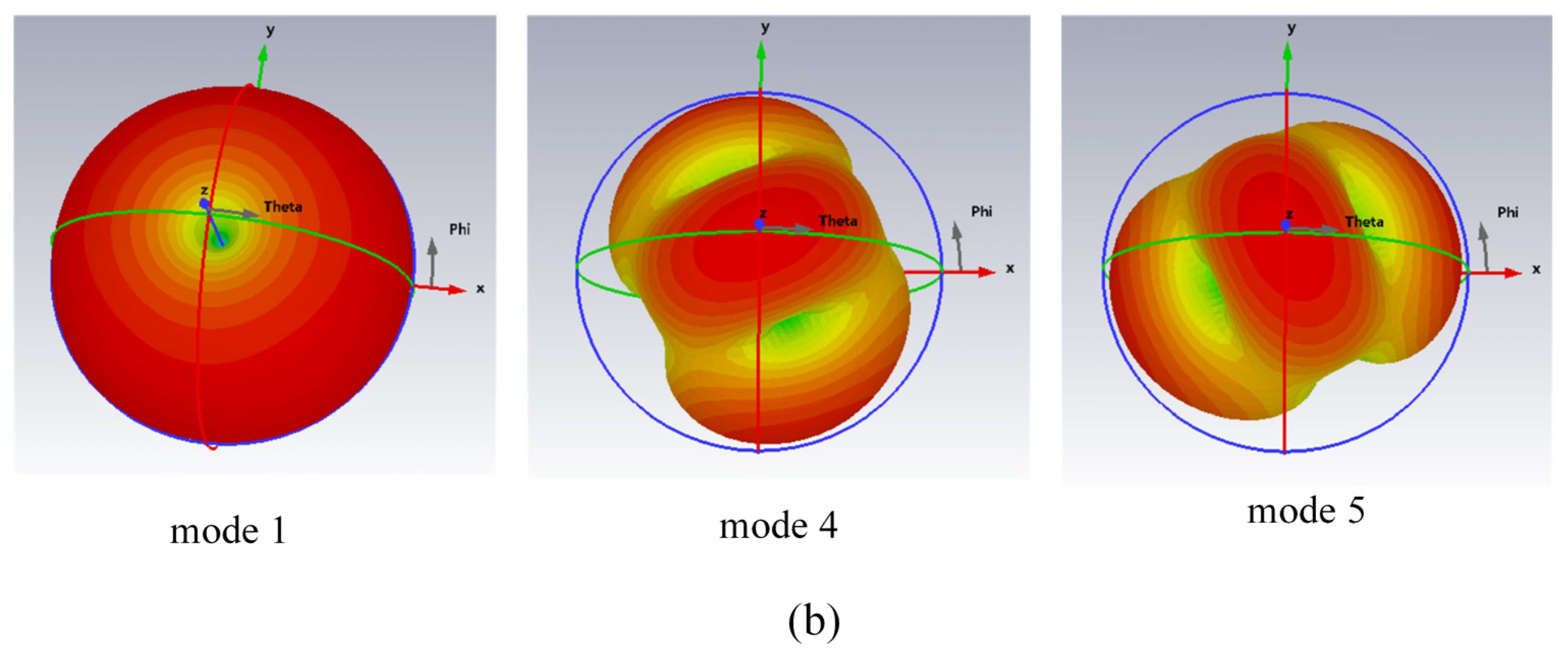
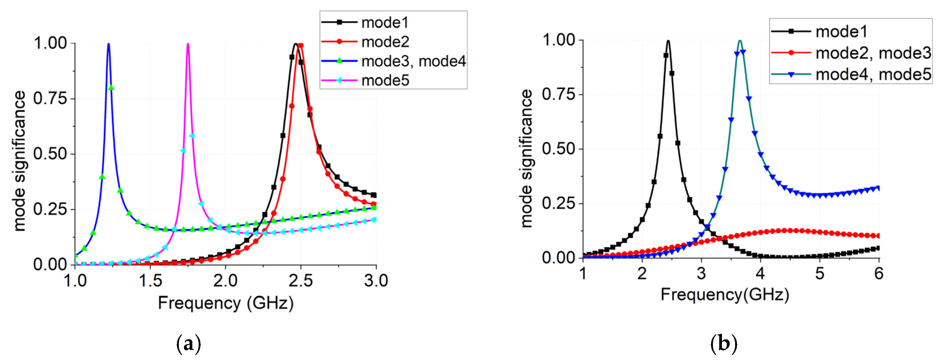
Figure 3 presents the far-field radiation patterns of the antennas in various working modes.
Figure 3a shows the radiation patterns corresponding to five modes for the conventional microstrip antenna, while
Figure 3b illustrates the patterns for three modes of the pin-loaded antenna structure. The conventional microstrip antenna exhibits omnidirectional radiation characteristics in modes 1, 2, and 5. Specifically, under mode 1—that is, when the operating frequency was 2.45 GHz—the microstrip antenna operated in the TM
22 mode. Similarly, the pin-loaded antenna structure achieves omnidirectional radiation when operating in mode 1, corresponding to the Quasi-TM
11 mode.
Figure 4a illustrates the different mode distributions of the conventional microstrip patch antenna, while
Figure 4b shows different mode distributions of the pin-loaded antenna.
It can be further obtained from
Figure 4 that the reference microstrip antenna has five modes within 1–3 GHz, and its working frequencies are 1.2 GHz, 1.75 GHz, 2.45 GHz, 2.5 GHz; meanwhile, the antenna II has three modes with 1–6 GHz, and the working frequencies are 2.45 GHz and 3.6 GHz respectively.
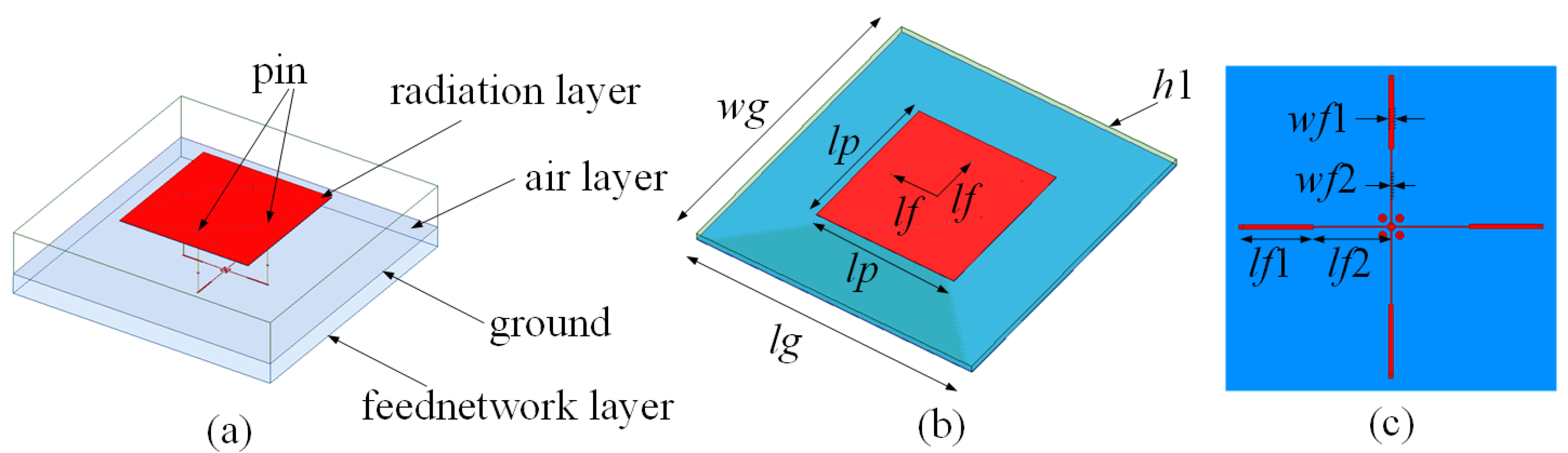
3. Array Antenna I
The structure of the antenna is illustrated in
Figure 5. The antenna consists of three layers: the radiation layer, the intermediate ground layer, and the feed signal layer. The dielectric substrate of the radiation layer and the power-division network layer are both made of S7136 material with a dielectric constant of 3.6, a loss tan of 0.0035, and a thickness of 0.508 mm. An air dielectric layer with a thickness of 5 mm is placed between the radiation layer and the ground layer of the power-division network. The structural dimensions of the antenna are as follows:
wg = 220 mm,
lg = 220 mm,
lp = 110 mm,
lf = 36 mm,
lf1 = 18 mm,
lf2 = 19 mm,
wf1 = 1.1 mm,
wf2 = 0.24 mm,
h = 5 mm, and
h1 = 0.508 mm.
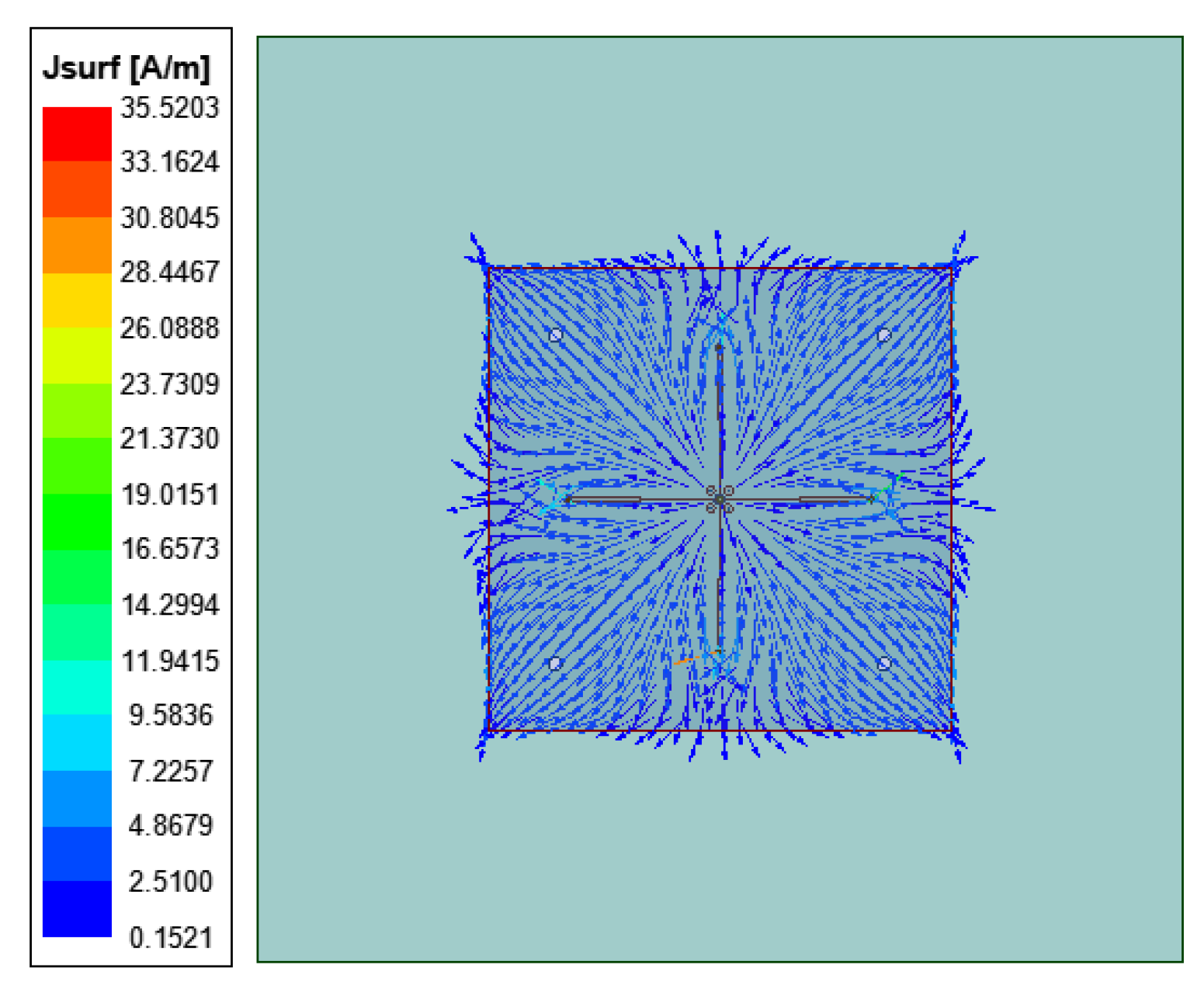
The surface current distribution of the antenna is shown in
Figure 6. When the excitation ports are of equal amplitude and the phases between adjacent ports have the same phase, the surface current of the antenna exhibits central symmetrical and omnidirectional characteristics.
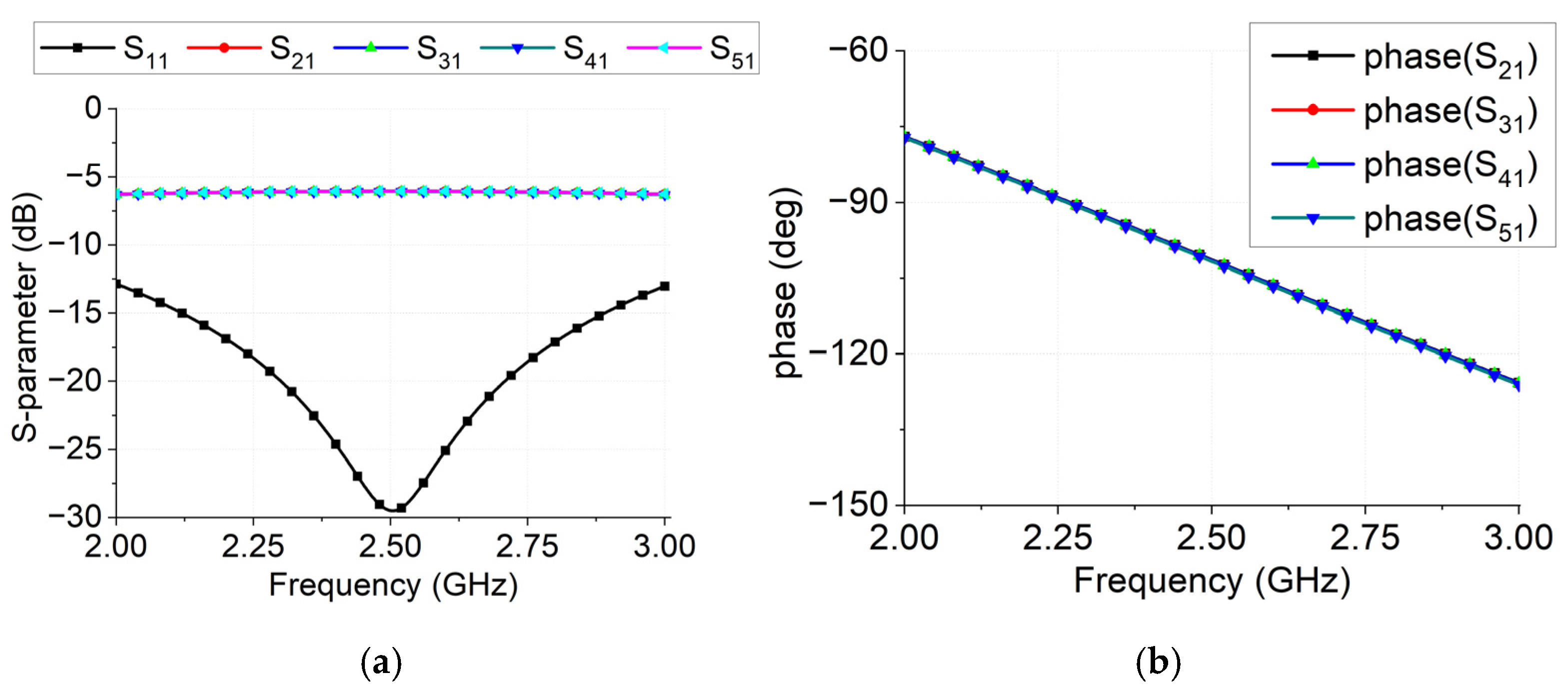
A power divider with transmission line theory was adopted for the feed network, as shown in
Figure 5c. The input port was located in the center (port 1), with output ports (ports 1, 2, 3, and 4) arranged around it (1:4 power divider).
The simulated reflection coefficient (S
11) and transmission coefficient (S
21, S
31, S
41, and S
51) of the 1:4 feed network are shown in
Figure 7. From
Figure 7a, one can see that for a bandwidth of 2.0–3.0 GHz, the S
11 of the input ports is below −10 dB, and the amplitudes of the output ports are approximately equal. At 2.45 GHz, the insertion loss is approximately 0.07 dB.
Figure 7b shows that the phases of each output terminal are identical, meeting the phase requirements of the output ports.
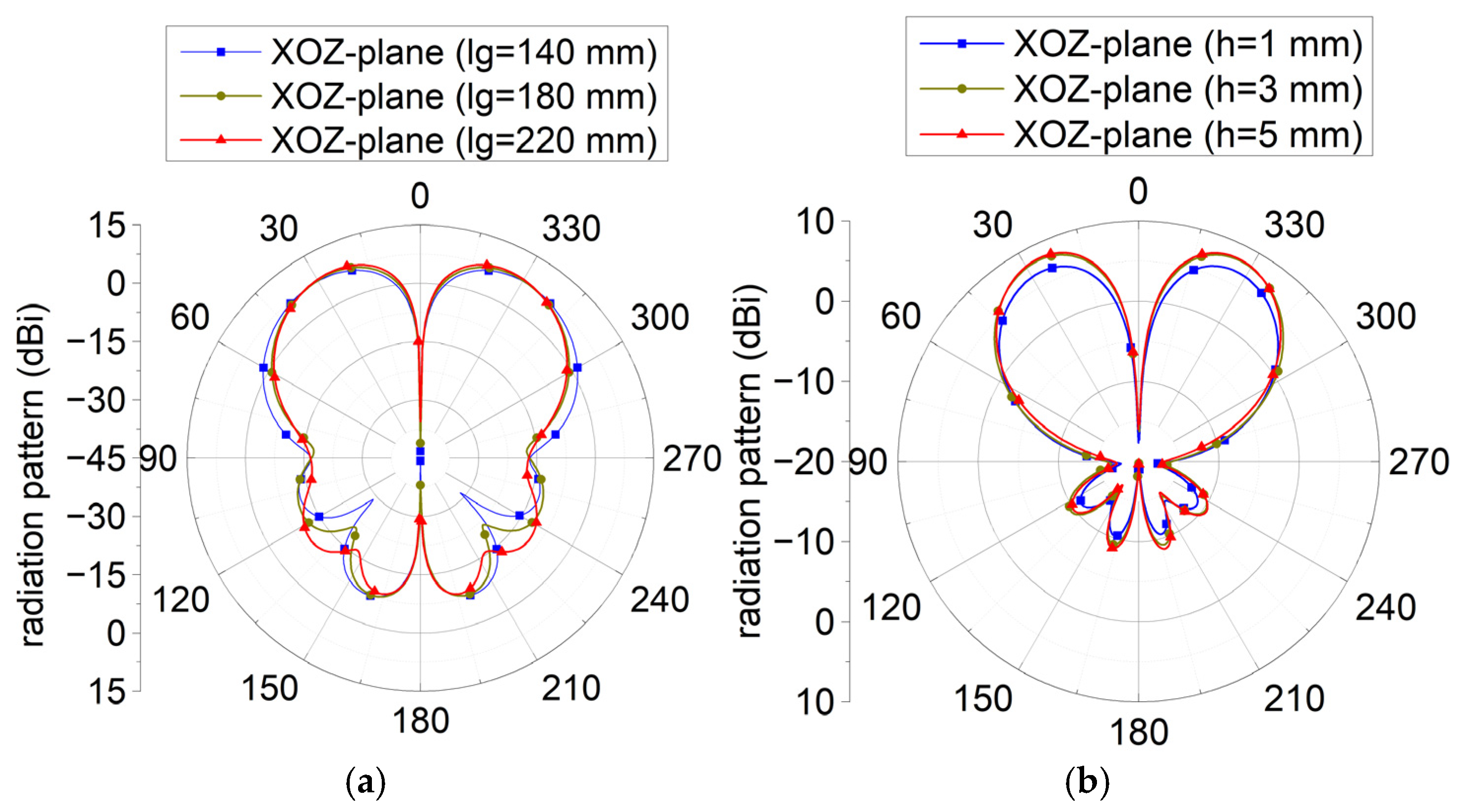
The antenna designed in this paper has an omnidirectional radiation pattern. To investigate the influence of the metal ground plate size on radiation pattern and gain, the simulation results for different ground plate sizes are shown in
Figure 8a. The XOZ-plane was selected to analyze the radiation pattern due to the high symmetry between the XOZ-plane and YOZ-plane. As shown in
Figure 8a, increasing the ground plate size from 140 mm to 220 mm raises the peak gain from 7.6 dBi to 8.2 dBi at 2.45 GHz. The peak gain position also shifts from θ = ±30° to θ = ±25°, moving towards the center.
Figure 8b shows the simulation results of the antenna’s radiation pattern with different air dielectric layer thicknesses. As the air layer thickness increases from 1 mm to 5 mm, the peak gain increases from 6.6 dBi to 8.2 dBi.
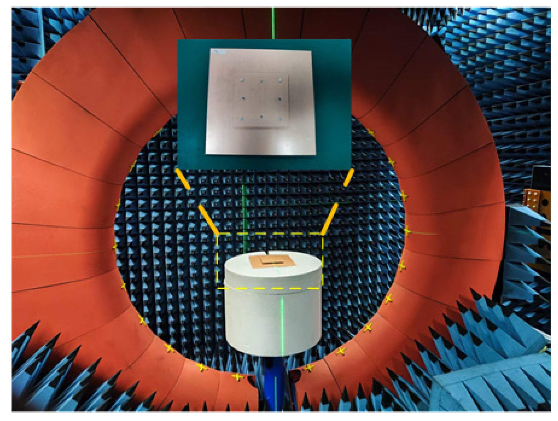
To verify the antenna’s performance, the antenna structure was fabricated, as shown in
Figure 9. The S
11 of the antenna was measured using a network analyzer, and the radiation patterns were measured in a near-field microwave anechoic chamber. The measurement results for the array antenna are shown in
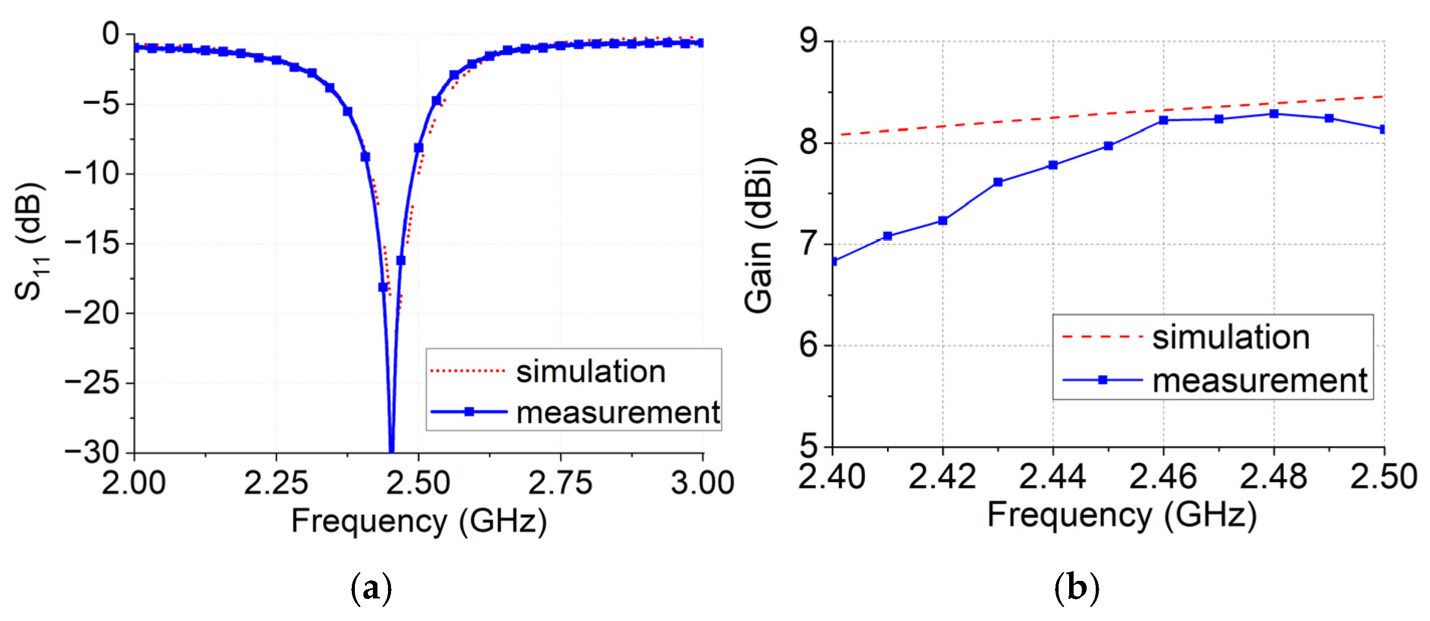
Figure 10. The −10 dB bandwidth of the antenna is 2.42–2.50 GHz (80 MHz). At 2.45 GHz, the S
11 is −20 dB. The antenna exhibits omnidirectional radiation with a peak gain of 8.0 dBi at 2.45 GHz.
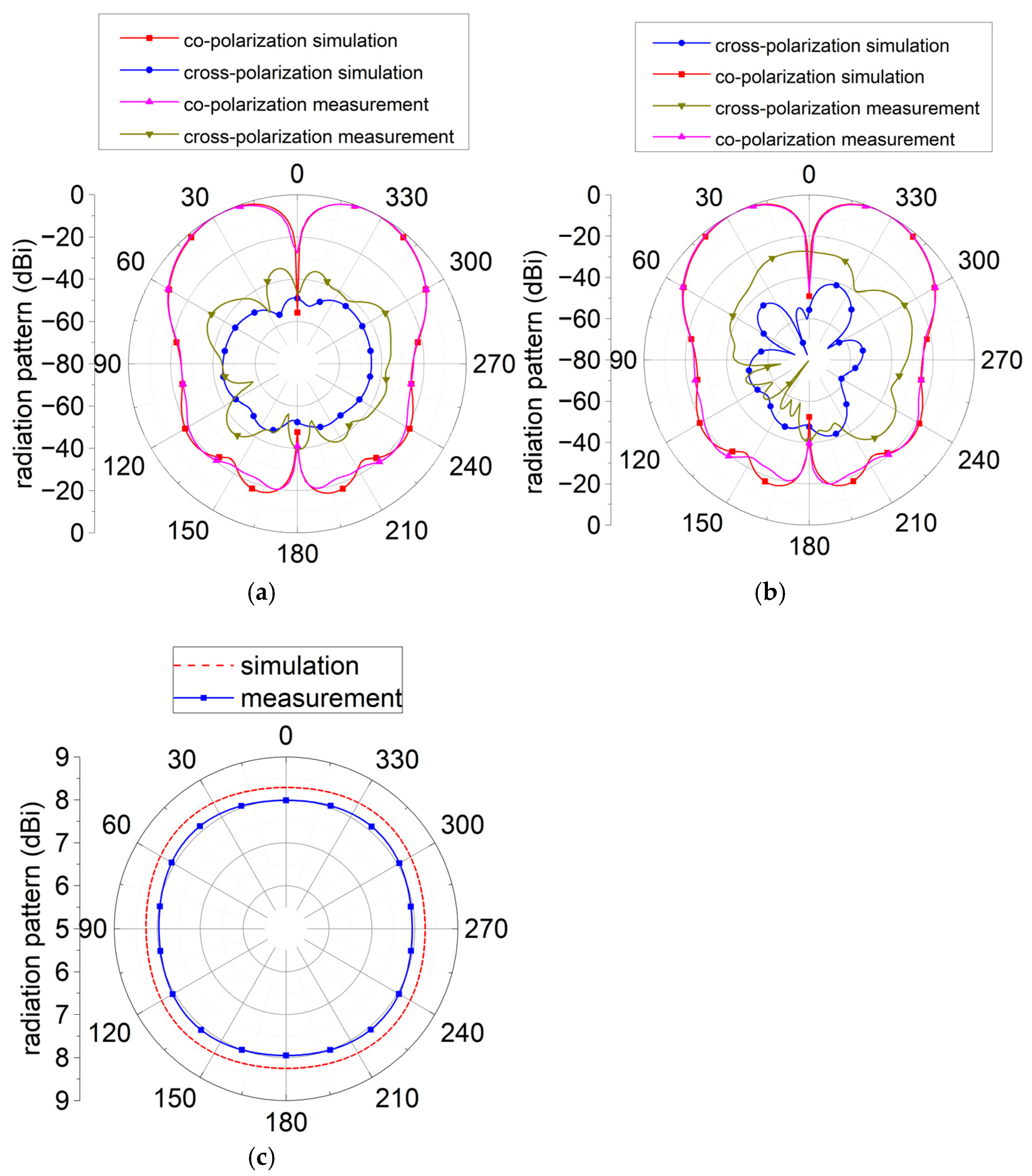
The radiation patterns of the antenna are shown in
Figure 11. The antenna demonstrates omnidirectional patterns similar to those of a dipole antenna in both the XOZ-plane and YOZ-plane, as shown in
Figure 11a,b. At θ = 28°, the peak gain is 8.0 dBi, as shown in
Figure 11c. The measured gain is 0.2 dBi lower than the simulated value due to antenna processing, assembly, and measurement errors. The antenna’s symmetrical surface current distribution, resulting from the four-fed structure, ensures low pattern ripple at 2.45 GHz.
4. Array Antenna II
Figure 12 depicts Antenna II’s structure. The antenna comprises multiple layers: the upper radiation layer, intermediate dielectric layer, lower metal ground layer, feed network dielectric layer, and feed signal layer. The dielectric substrate of the radiation layer is also the S7136 material with a thickness of 0.508 mm.
The structural dimensions of the antenna are as follows: wg = 124 mm, lg = 124 mm, l2 = 62 mm, w2 = 62 mm, lp1 = 10 mm, lp2 = 18 mm, rp = 1.0 mm, h1 = 3 mm, h2 = 0.508 mm, wf1 = 1 mm, lf1 = 2 mm, lf2 = 1 mm, wf2 = 0.24 mm, lf3 = 6 mm, lf4 = 2 mm, and lf5 = 5 mm.
The current analysis of the antenna radiation patch structure is shown in
Figure 13, from which it can be observed that when the amplitudes of each excitation port are equal and in phase, the current shows a central symmetric relationship such that the antenna has omnidirectional radiation characteristics.
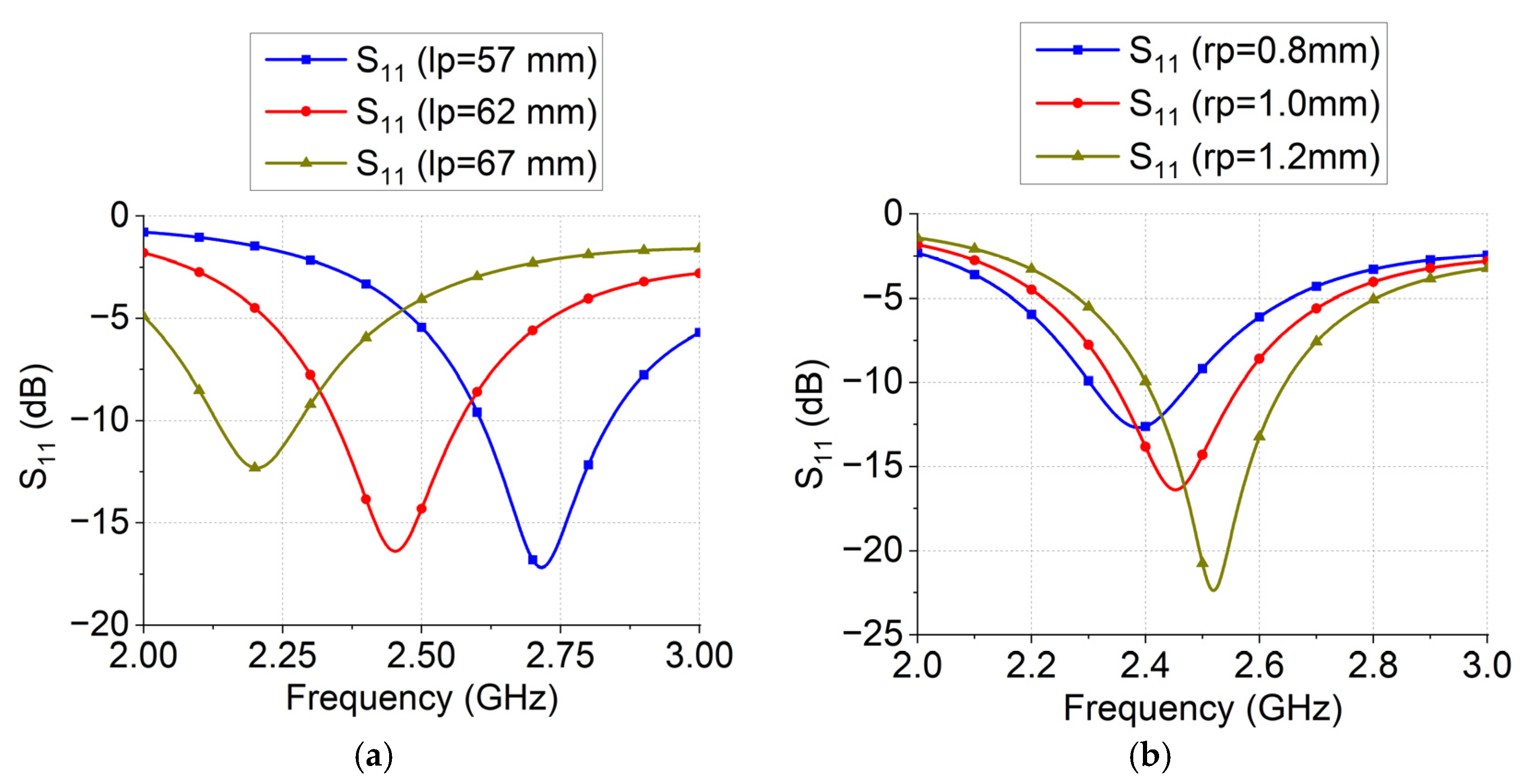
To analyze the influence of structural parameters on antenna performance, the following parameters are investigated: the length of the radiation patch, and the radius of the metal probe. The simulation results are shown in
Figure 14.
As shown in
Figure 14a, the length of the patch significantly affects the antenna’s S
11. As the patch length increases, the resonant frequency shifts to lower frequencies.
Figure 14b illustrates the influence of the metal probe radius on the antenna’s S
11. As the radius increases, the resonant frequency shifts to higher frequencies. Through the theoretical analysis of microstrip antenna, the antenna designed in this study mainly works in the high-order mode of the antenna. The increase of the metal probe is equivalent to the smaller size of the effective radiation patch so that the resonant frequency of the antenna changes to the high frequency.
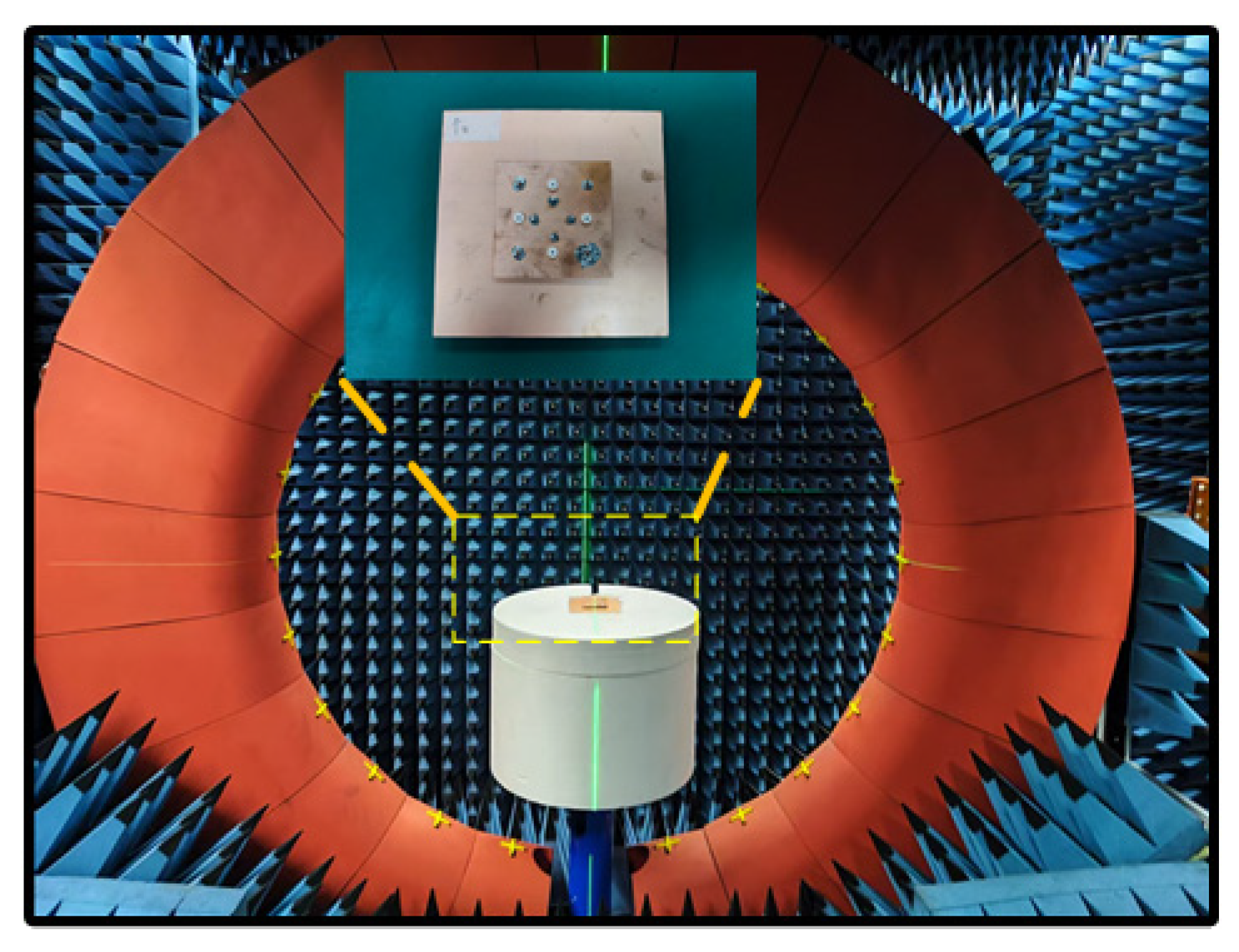
The antenna structure was fabricated and its performance was evaluated, as shown in
Figure 15. The S
11 of the antenna was measured using a network analyzer, and the radiation patterns were measured in a near-field microwave anechoic chamber. The measurement results are shown in
Figure 16 and
Figure 17.
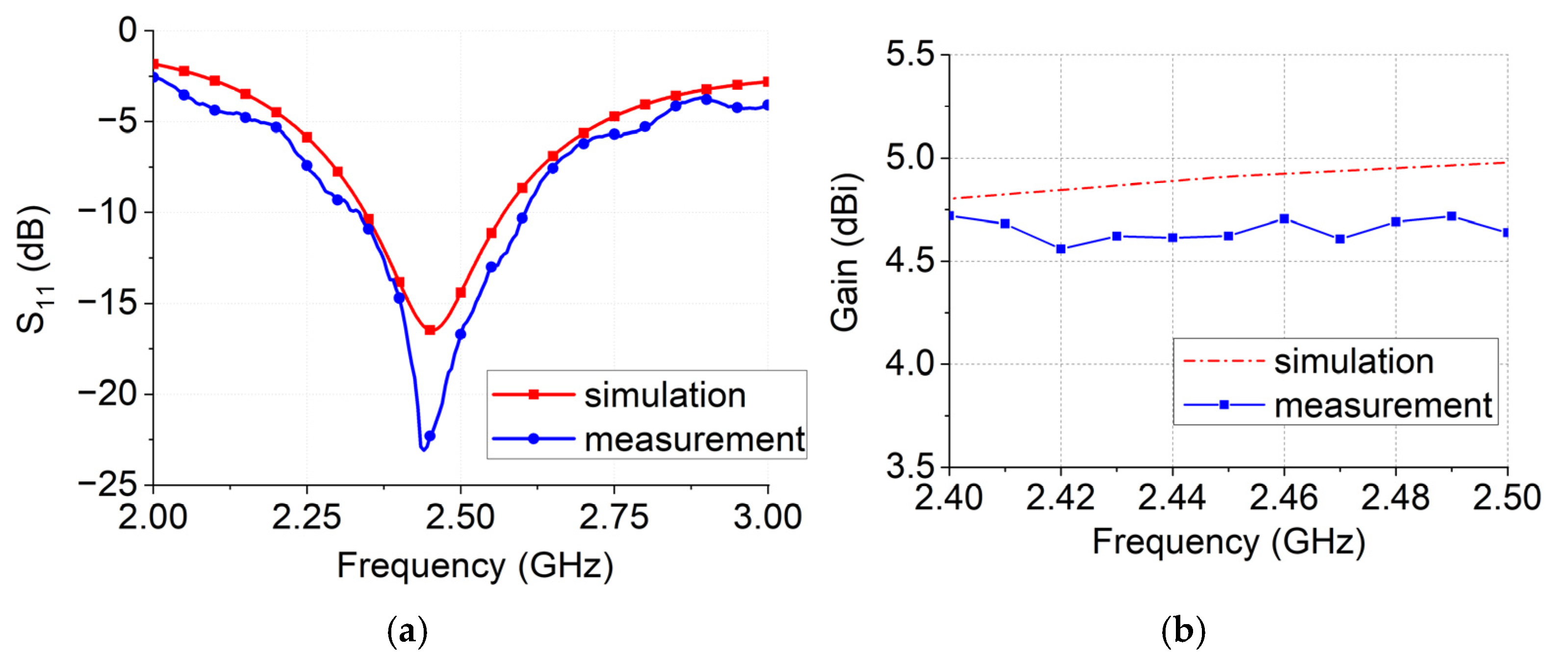
Figure 16 shows the S
11 measurement results for Antenna II. The antenna exhibits a −10 dB bandwidth of 2.34–2.57 GHz, with an S
11 of −16.4 dB at 2.45 GHz.
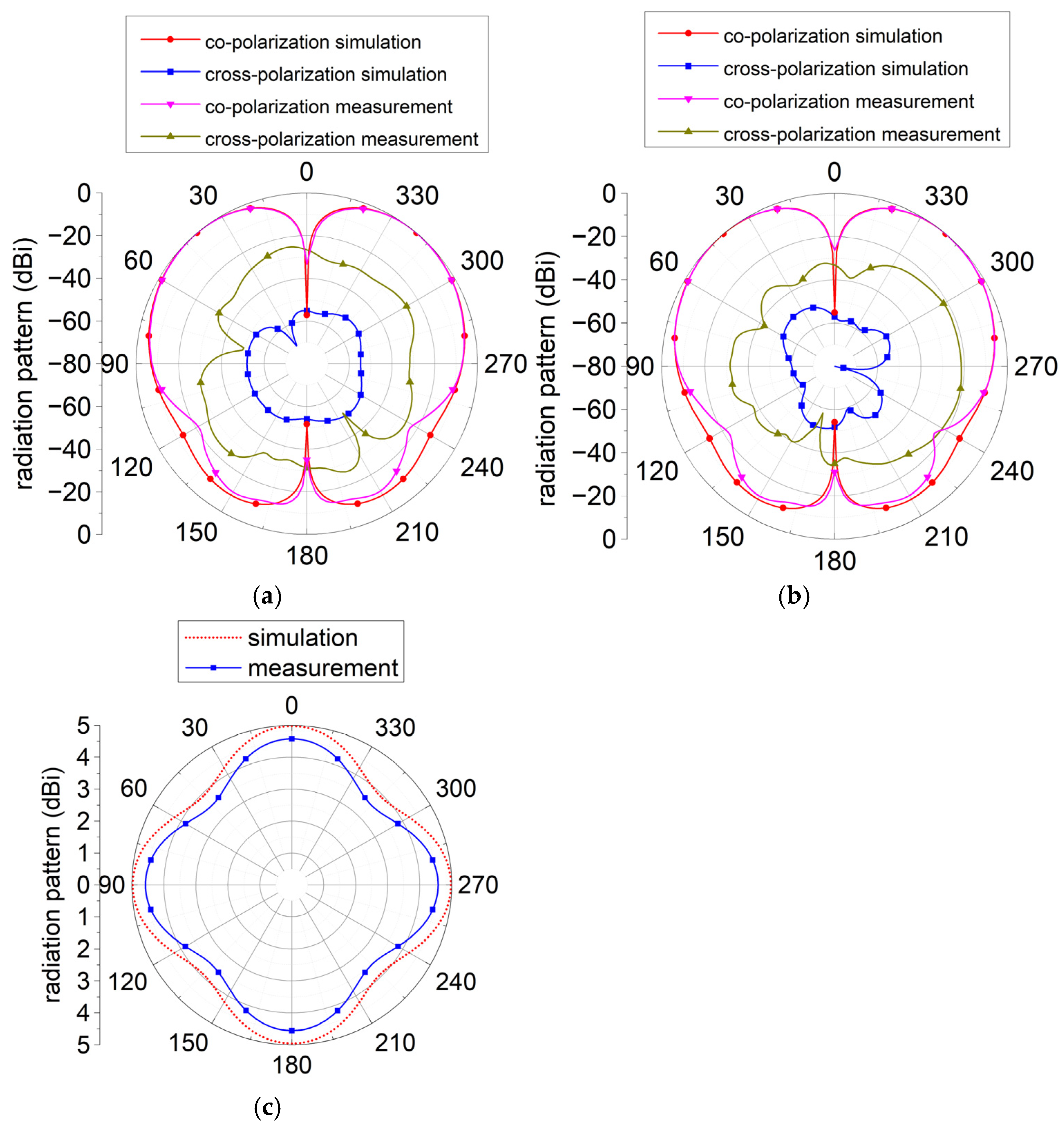
Figure 17 shows the simulated and measured results for the radiation patterns of Antenna II. At 2.45 GHz, the antenna demonstrates omnidirectional radiation characteristics in both the XOZ and YOZ planes, with a gain of approximately 4.55 dBi. The cross-polarization ratios on the XOZ and YOZ planes are 49.3 dB and 50.1 dB, respectively. The antenna exhibits less than a 0.2 dB pattern ripple at 2.45 GHz. The peak gain occurs at θ = 36°, as shown in
Figure 17c.
5. Performance Comparison
In this section, we compare the performance of the proposed omnidirectional antennas with those reported in the literature. As
Table 1 shows, the peak gains of Antennas I and II at 2.45 GHz are 8.0 dBi and 4.55 dBi, respectively.
Antenna 1 mainly operates in the TM22 mode, while Antenna II mainly works in the quasi-TM11 mode. Antenna I is larger in size than Antenna II. According to antenna theory, if the radiation aperture of the antenna is larger, while the thickness of the antenna dielectric layer is greater, then the gain of the antenna will be higher. Therefore, compared with Antenna II, Antenna I has a higher gain. Considering the four-metal probe in Antenna 2, the bandwidths of Antennas 1 and 2 are slightly different.
These gains are competitive with those of similar omnidirectional antennas reported in [
13,
18,
19,
20,
22]. Notably, Antenna II achieves a height of 0.028λ
0, which is significantly lower than that of other comparable omnidirectional antennas [
13,
19,
22]. This low-profile design enhances the integration potential of the antenna in compact systems.
Both Antennas I and II are vertically polarized, making them suitable for deployment in metal grounding environments. This feature is particularly advantageous for applications such as wireless energy harvesting, where vertical polarization is often preferred for optimal performance.
6. Conclusions
This study employed characteristic mode theory (CMT) to analyze and design two distinct omnidirectional antennas for high-performance wireless communication applications. Antenna I, based on a high-order TM22-mode microstrip structure, achieved a peak gain of 8.0 dBi at 2.45 GHz, while Antenna II, utilizing a pin-loaded TM11-mode configuration, demonstrated a gain of 4.55 dBi at the same operating frequency. Both antennas were fed by a 1:4 power divider, ensuring uniform excitation and low pattern ripple. The proposed antennas exhibit several notable advantages. Antenna I offers high gain and a compact profile, making it suitable for applications requiring high directivity and efficient energy transfer. Antenna II, with its low profile (0.028λ0) and omnidirectional radiation pattern, is particularly well-suited for integration into compact systems and environments with metal grounding. Both antennas are vertically polarized, enhancing their applicability in wireless energy harvesting and other wireless communication scenarios.
Author Contributions
Conceptualization, T.T. and L.P.; methodology, W.H. and D.T.; experimental, D.T. and M.A.A.; data curation, T.S.A.; writing—original draft preparation, M.A.A.; writing—review and editing, W.H. and T.S.A.; Funding acquisition, W.H., T.T. and T.S.A. All authors have read and agreed to the published version of the manuscript.
Funding
This work was supported by the Southwest Minzu University Research Startup Funds (RQD2021060) and the Sichuan Provincial Science and Technology Department Key Project (2025YFHZ0013). This study is also supported by funding from Prince Sattam bin Abdulaziz University project (PSAU/2025/1446).
Data Availability Statement
The original contributions presented in the study are included in the article; further inquiries can be directed to the corresponding author/s.
Conflicts of Interest
The authors declare no conflicts of interest regarding the publication of this article.
References
- Lei, S.; Li, X.; Han, K.; Wei, G. A Design of Simple Vertically Polarized Vivaldi-Based Omnidirectional Antenna for X-Band. In Proceedings of the 2021 IEEE 4th International Conference on Electronics Technology (ICET), Chengdu, China, 7–10 May 2021; pp. 622–626. [Google Scholar] [CrossRef]
- Zhou, L.; Jiao, Y.; Qi, Y.; Weng, Z.; Lu, L. Wideband Ceiling-Mount Omnidirectional Antenna for Indoor Distributed Antenna Systems. IEEE Antennas Wirel. Propag. Lett. 2014, 13, 836–839. [Google Scholar] [CrossRef]
- Chreim, H.; Pointereau, E.; Jecko, B.; Dufrane, P. Omnidirectional Electromagnetic Band Gap Antenna for Base Station Applications. IEEE Antennas Wirel. Propag. Lett. 2007, 6, 499–502. [Google Scholar] [CrossRef]
- Kamal, M.M.; Yang, S.; Ren, X.C.; Altaf, A.; Kiani, S.H.; Anjum, M.R.; Iqbal, A.; Asif, M.; Saeed, S.I. Infinity Shell Shaped MIMO Antenna Array for Mm-Wave 5G Applications. Electronics 2021, 10, 165. [Google Scholar] [CrossRef]
- Abubakar, H.S.; Zhao, Z.; Kiani, S.H.; Khan, S.; Ali, T.; Bashir, M.A.; Cengiz, K.; Kamal, M.M. Eight Element MIMO Antenna for Sub 6 GHz 5G Cellular Devices. Phys. Scr. 2024, 99, 085559. [Google Scholar] [CrossRef]
- Kamal, M.M.; Wang, B.; Shoaib, N.; Rafque, U.; Abbasi, M.I.; Kamarudin, M.R. Self-Decoupled Quad-Port CPW-Fed Fractal MIMO Antenna with UWB Characteristics. Int. J. Antennas Propag. 2024, 2024, 3826899. [Google Scholar] [CrossRef]
- Economou, L.; Langley, J. Patch antenna equivalent to simple monopole. Electron. Lett. 1997, 9, 727–729. [Google Scholar] [CrossRef]
- Al-Zoubi, A.; Yang, F.; Kishk, A. A Broadband Center-Fed Circular Patch-Ring Antenna with a Monopole like Radiation Pattern. IEEE Trans. Antennas Propag. 2009, 57, 789–792. [Google Scholar] [CrossRef]
- Liu, J.; Xue, Q.; Wong, H.; Lai, H.W.; Long, Y. Design and Analysis of a Low-Profile and Broadband Microstrip Monopolar Patch Antenna. IEEE Trans. Antennas Propag. 2013, 61, 11–18. [Google Scholar] [CrossRef]
- Liu, J.; Zheng, S.; Li, Y.; Long, Y. Broadband Monopolar Microstrip Patch Antenna with Shorting Vias and Coupled Ring. IEEE Antennas Wirel. Propag. Lett. 2014, 13, 39–42. [Google Scholar] [CrossRef]
- Zhai, X.; Zhu, L.; Liu, Q. A Low-Profile Vertically Polarized Patch Antenna with Wideband Omnidirectional Radiation Based on Triple Resonant Modes. IEEE Antennas Wirel. Propag. Lett. 2024, 24, 73–77. [Google Scholar] [CrossRef]
- Oh, J.; Sarabandi, K. Low Profile Vertically Polarized Omnidirectional Wideband Antenna with Capacitively Coupled Parasitic Elements. IEEE Trans. Antennas Propag. 2014, 62, 977–982. [Google Scholar] [CrossRef]
- Wen, S.; Dong, Y. A Low-Profile Vertically Polarized Antenna with Conical Radiation Pattern for Indoor Micro Base Station Application. IEEE Antennas Wirel. Propag. Lett. 2021, 20, 169–173. [Google Scholar] [CrossRef]
- Deng, C.; Li, P.; Cao, W. Low-Profile Patch Antennas with Vertical Monopole-like Radiation Patterns Based on Modified Capacitive Coupling Structures. IEEE Antennas Wirel. Propag. Lett. 2012, 11, 1354–1357. [Google Scholar] [CrossRef]
- Sun, L.; Li, Y.; Zhang, Z.; Feng, Z. Compact Co-Horizontally Polarized Full-Duplex Antenna with Omnidirectional Patterns. IEEE Antennas Wirel. Propag. Lett. 2019, 18, 1154–1158. [Google Scholar] [CrossRef]
- Sun, L.; Li, Y.; Zhang, Z.; Iskander, M.F. A Compact Planar Omnidirectional MIMO Array Antenna with Pattern Phase Diversity Using Folded Dipole Element. IEEE Trans. Antennas Propag. 2019, 67, 1688–1696. [Google Scholar] [CrossRef]
- Yu, Y.; Jolani, F.; Chen, Z. A Wideband Omnidirectional Horizontally Polarized Antenna for 4G LTE Applications. IEEE Antennas Wirel. Propag. Lett. 2013, 12, 686–689. [Google Scholar] [CrossRef]
- Wang, Z.D.; Yin, Y.Z.; Yang, X.; Wu, J.J. Design of a Wideband Horizontally Polarized Omnidirectional Antenna with Mutual Coupling Method. IEEE Trans. Antennas Propag. 2015, 63, 3311–3316. [Google Scholar] [CrossRef]
- Yu, Y.; Xiong, J.; Wang, R. A Wideband Omnidirectional Antenna Array with Low Gain Variation. IEEE Antennas Wirel. Propag. Lett. 2016, 15, 386–389. [Google Scholar] [CrossRef]
- Ye, L.H.; Zhang, Y.; Zhang, X.Y.; Xue, Q. Broadband Horizontally Polarized Omnidirectional Antenna Array for Base-Station Applications. IEEE Trans. Antennas Propag. 2019, 67, 2792–2797. [Google Scholar] [CrossRef]
- Yang, X.; Liu, Y.; Gong, S.X. Design of a Wideband Omnidirectional Antenna with Characteristic Mode Analysis. IEEE Antennas Wirel. Propag. Lett. 2018, 17, 993–997. [Google Scholar] [CrossRef]
- Shuai, S.; Su, H.; Jiao, Y.; Ou, J.H.; Zhang, X.Y. Ultra-Wideband Omnidirectional Antenna with Stable Radiation Patterns Using CMA. IEEE Trans. Veh. Technol. 2024, 73, 10788–10792. [Google Scholar] [CrossRef]
- Sathishkumar, N.; Palanisamy, S.K.; Natarajan, R.; Ouahada, K.; Hamam, H. Design of Dual Mode Antenna Using CMA and Broadband Dual-Polarized Antenna for 5G Networks. Sci. Rep. 2024, 14, 15553. [Google Scholar] [CrossRef]
- Li, T.; Gao, J.; Rasool, N.; Basit, M.A.; Chen, C. Characteristic Mode-Based Dual-Mode Dual-Band of Single-Feed Antenna for On-/Off-Body Communication. Electronics 2024, 13, 2733. [Google Scholar] [CrossRef]
- Anchidin, L.; Lavric, A.; Mutescu, P.M.; Petrariu, A.I.; Popa, V. The Design and Development of a Microstrip Antenna for Internet of Things Applications. Sensors 2023, 23, 1062. [Google Scholar] [CrossRef]
- Zhang, X.; Zhu, L. Gain-Enhanced Patch Antenna without Enlarged Size via Loading of Slot and Shorting Pins. IEEE Trans. Antennas Propag. 2017, 65, 5702–5709. [Google Scholar] [CrossRef]
- Zhang, X.; Zhu, L. High-Gain Circularly Polarized Microstrip Patch Antenna with Loading of Shorting Pins. IEEE Trans. Antennas Propag. 2016, 64, 2172–2178. [Google Scholar] [CrossRef]
- Zhang, X.; Zhu, L. Patch Antennas with Loading of a Pair of Shorting Pins Toward Flexible Impedance Matching and Low Cross Polarization. IEEE Trans. Antennas Propag. 2016, 64, 1226–1233. [Google Scholar] [CrossRef]
- Computer Simulation Technology. Available online: https://www.3ds.com (accessed on 1 January 2024).
Figure 1.
Antenna design process. (a) Conventional microstrip antenna for TM10 mode. (b) Pin-loaded microstrip antenna for Quasi-TM11 mode.
Figure 1.
Antenna design process. (a) Conventional microstrip antenna for TM10 mode. (b) Pin-loaded microstrip antenna for Quasi-TM11 mode.
Figure 2.
Simulation diagram of characteristic mode analysis for Antenna II.
Figure 2.
Simulation diagram of characteristic mode analysis for Antenna II.
Figure 3.
Radiation pattern of antennas with different modes. (a) Conventional microstrip antenna. (b) Pin-loading antenna.
Figure 3.
Radiation pattern of antennas with different modes. (a) Conventional microstrip antenna. (b) Pin-loading antenna.
Figure 4.
Modes of antenna. (a) Conventional microstrip antenna, (b) Pin-loaded antenna.
Figure 4.
Modes of antenna. (a) Conventional microstrip antenna, (b) Pin-loaded antenna.
Figure 5.
Antenna I structure. (a) 3D view. (b) Radiation layer. (c) Feed network layer.
Figure 5.
Antenna I structure. (a) 3D view. (b) Radiation layer. (c) Feed network layer.
Figure 6.
Surface current distribution of Antenna I.
Figure 6.
Surface current distribution of Antenna I.
Figure 7.
Simulation results of feed network. (a) Amplitudes. (b) Phase.
Figure 7.
Simulation results of feed network. (a) Amplitudes. (b) Phase.
Figure 8.
Parameters analysis of Antenna I. (a) Ground length. (b) Height of air layer.
Figure 8.
Parameters analysis of Antenna I. (a) Ground length. (b) Height of air layer.
Figure 9.
Radiation pattern measurement of Antenna I.
Figure 9.
Radiation pattern measurement of Antenna I.
Figure 10.
S11 and gain simulated and measured results of Antenna I. (a) S11. (b) Gain.
Figure 10.
S11 and gain simulated and measured results of Antenna I. (a) S11. (b) Gain.
Figure 11.
Radiation patterns of Antenna I. (a) XOZ-plane. (b) YOZ-plane. (c) Peak gain of θ = 28°.
Figure 11.
Radiation patterns of Antenna I. (a) XOZ-plane. (b) YOZ-plane. (c) Peak gain of θ = 28°.
Figure 12.
Antenna II structure. (a) 3D view. (b) Radiation layer. (c) Feed network.
Figure 12.
Antenna II structure. (a) 3D view. (b) Radiation layer. (c) Feed network.
Figure 13.
Surface current distribution of Antenna II.
Figure 13.
Surface current distribution of Antenna II.
Figure 14.
Parameters analysis of Antenna II. (a) Length of patch. (b) Radius of the metal probe.
Figure 14.
Parameters analysis of Antenna II. (a) Length of patch. (b) Radius of the metal probe.
Figure 15.
Radiation patterns measurement of Antenna II.
Figure 15.
Radiation patterns measurement of Antenna II.
Figure 16.
S11and gain simulated and measured results of Antenna II. (a) S11. (b) Gain.
Figure 16.
S11and gain simulated and measured results of Antenna II. (a) S11. (b) Gain.
Figure 17.
Radiation patterns of Antenna II. (a) XOZ plane. (b) YOZ plane. (c) Peak gain of θ = 36°.
Figure 17.
Radiation patterns of Antenna II. (a) XOZ plane. (b) YOZ plane. (c) Peak gain of θ = 36°.
Table 1.
Comparison with other designs.
Table 1.
Comparison with other designs.
| Reference | Bandwidth (GHz) | Polarization | Peak Gain (dBi) at 2.45 GHz | Size (λ03)
λ0 at 2.45 GHz |
|---|
| [13] | 1.7–2.79 | vertical | 4.5 | 0.26 × 0.26 × 0.086 |
| [18] | 1.7–3.54 | horizontal | 0.6 | 1.225 × 1.225 × 0.0086 |
| [19] | 1.62–2.75 | vertical | 4.7 | 0.62 × 0.62 × 0.77 |
| [20] | 1.67–2.73 | horizontal | 1.7 | 0.98 × 0.98 × 0.0058 |
| [22] | 1.7–5.0 | vertical | 3.2 | 0.36 × 0.36 × 0.49 |
| This work | Antenna I | 2.42–2.5 | vertical | 8.0 | 1.76 × 1.76 × 0.048 |
| Antenna II | 2.34–2.57 | vertical | 4.55 | 0.99 × 0.99 × 0.028 |
| Disclaimer/Publisher’s Note: The statements, opinions and data contained in all publications are solely those of the individual author(s) and contributor(s) and not of MDPI and/or the editor(s). MDPI and/or the editor(s) disclaim responsibility for any injury to people or property resulting from any ideas, methods, instructions or products referred to in the content. |
© 2025 by the authors. Licensee MDPI, Basel, Switzerland. This article is an open access article distributed under the terms and conditions of the Creative Commons Attribution (CC BY) license (https://creativecommons.org/licenses/by/4.0/).


 ,
, 


