1. Introduction
The world’s currently high demand for energy, combined with increasingly stringent regulations focused on sustainability and eco-friendly designs (ecodesign) [
1,
2,
3], has created a strong need to optimize energy conversion systems. As industries seek more energy-efficient solutions, the integration of renewable sources and the development of advanced technologies become crucial. In this context, power converters, particularly DC–DC converters, play an essential role, being key components in a wide variety of industrial, consumer, and mobility applications, including electric vehicles and power management systems. These converters are responsible for adapting voltages in power conditioning systems, making the optimization of their operation critical for enhancing energy efficiency and achieving sustainable designs.
Traditionally, DC–DC converters employ hard-switching techniques to transfer power from the source to the load through controlled switches. However, this method is associated with two primary types of losses: conduction losses [
4,
5,
6], due to the resistive components, and switching losses, which arise from the overlap of current and voltage during power semiconductor device switching [
7,
8,
9]. Although the hard-switching method has relatively fast transitions using power semiconductor devices, the switching process is not instantaneous, resulting in significant power dissipation, especially at high operating frequencies. To minimize these losses while maintaining high-frequency operation, which is necessary to reduce component size and maximize power density, alternative approaches are required.
To address these limitations, soft-switching techniques have emerged as a solution to reduce switching losses. By modifying the current or voltage waveform during switching transitions, soft-switching allows power losses to be minimized by ensuring that the voltage or current is near zero when the switch is activated. Resonant converters, which incorporate an
LC resonant tank to smooth transitions, represent a significant advance over hard-switching. These converters can be further classified into quasi-resonant converters (QRC) and multi-resonant converters (MRC), depending on how many switches are associated with resonant circuits [
10,
11,
12,
13,
14]. Moreover, quasi-resonant converters employ techniques such as zero voltage switching (ZVS) [
15,
16] or zero current switching (ZCS) [
17,
18] that allow for either voltage or current to be zero during switching, to increase frequency and optimize efficiency. Another classification is based on the way in which the resonant cycle is operated, distinguishing between full-wave and half-wave operation. In half-wave quasi-resonant converters, the internal diode of the power switch conducts during part of the cycle. In full-wave quasi-resonant converters, an extra diode is added to block this internal diode, allowing better control of the switching process. The full-wave configuration provides better load regulation compared to the half-wave counterpart, maintaining a nearly constant switching frequency despite load variations. However, the addition of an extra component increases cost and space requirements. This makes the full-wave converter more stable when the load changes, ensuring a more consistent operation, but assuming the addition of one additional diode.
In addition to these considerations, in applications where bipolar symmetric outputs are required, single-input bipolar symmetric output (SIBSO) and single-input multiple-output (SIMO) DC–DC converters have grown in relevance [
19,
20,
21]. These converters are used in various applications, including lighting, auxiliary power supplies, and electric vehicle systems. Although traditional SIBSO converters are based on isolated transformers to generate bipolar outputs, these designs often suffer from inefficiencies and complexity due to the need for multiple controllers. However, transformerless SIBSO converters, which remove the need for isolation transformers, have emerged as a promising alternative, providing higher efficiency and power density. The use of new wide-bandgap semiconductors [
22,
23,
24,
25,
26] like gallium nitride (GaN) field effect transistor (FET) [
27,
28] further enhances the efficiency of these converters by enabling high-frequency operation and reducing switching losses.
Furthermore, the implementation of wide-bandgap semiconductor devices such as GaN FET and Silicon Carbide (SiC) is transforming converter design. These materials allow for higher frequency operation with reduced switching losses, resulting in greater power density and efficiency. The combination of these technologies with soft-switching techniques presents a promising pathway toward the miniaturization and optimization of converters. As designs become more compact and efficient, electronic systems benefit from improved thermal management, lower cooling requirements, and increased reliability.
As technology advances and electrical applications become more complex, the demand for efficient and versatile power conversion solutions increases. The need for devices capable of handling multiple outputs and operating reliably under various conditions has led to special attention being focused on the development of power converters. SIBSO converters are not limited to conventional applications such as power supplies and audio systems but are also gaining acceptance in emerging areas like solar energy and electric vehicles. In these contexts, the ability to generate symmetric outputs while maintaining high efficiency is critical to ensure optimal performance and economic viability of systems.
Moreover, it is essential to consider the impact that enhanced efficiency in DC–DC converters has on sustainability and the environment. As the transition toward renewable energy sources advances, the integration of efficient converters becomes crucial for maximizing the utilization of these sources. Well-designed converters not only reduce energy losses but also help decrease the carbon footprint of electrical systems. By promoting research and development of more sustainable energy conversion technologies, a precedent is set for the design of electrical systems that support a more efficient future.
This paper introduces a novel transformerless SIBSO DC–DC converter, utilizing GaN FET devices and soft-switching techniques to achieve high power density and efficiency. The proposed design incorporates just one gate-driven switch so that a single input can generate two bipolar outputs with common ground. The switch is grounded, eliminating the need for isolated sensors or drivers. ZVS is accomplished across the full load range, resulting in a more compact and cost-effective solution suitable for modern high-efficiency applications.
The rest of this paper is organized as follows:
Section 2 and
Section 3 introduce the converter topology and describe and provide a theoretical study of the novel converter operating modes, including modeling and circuit behavior under different operating conditions.
Section 4 details the component selection and practical considerations to develop the converter.
Section 5 presents the simulation results that validate the analysis and illustrate the converter’s performance.
Section 6 develops a model to quantify losses, assessing overall efficiency.
Section 7 presents measurements from the prototype, comparing them with theoretical and simulated results to validate the proper operation, and finally,
Section 8 ends with conclusions.
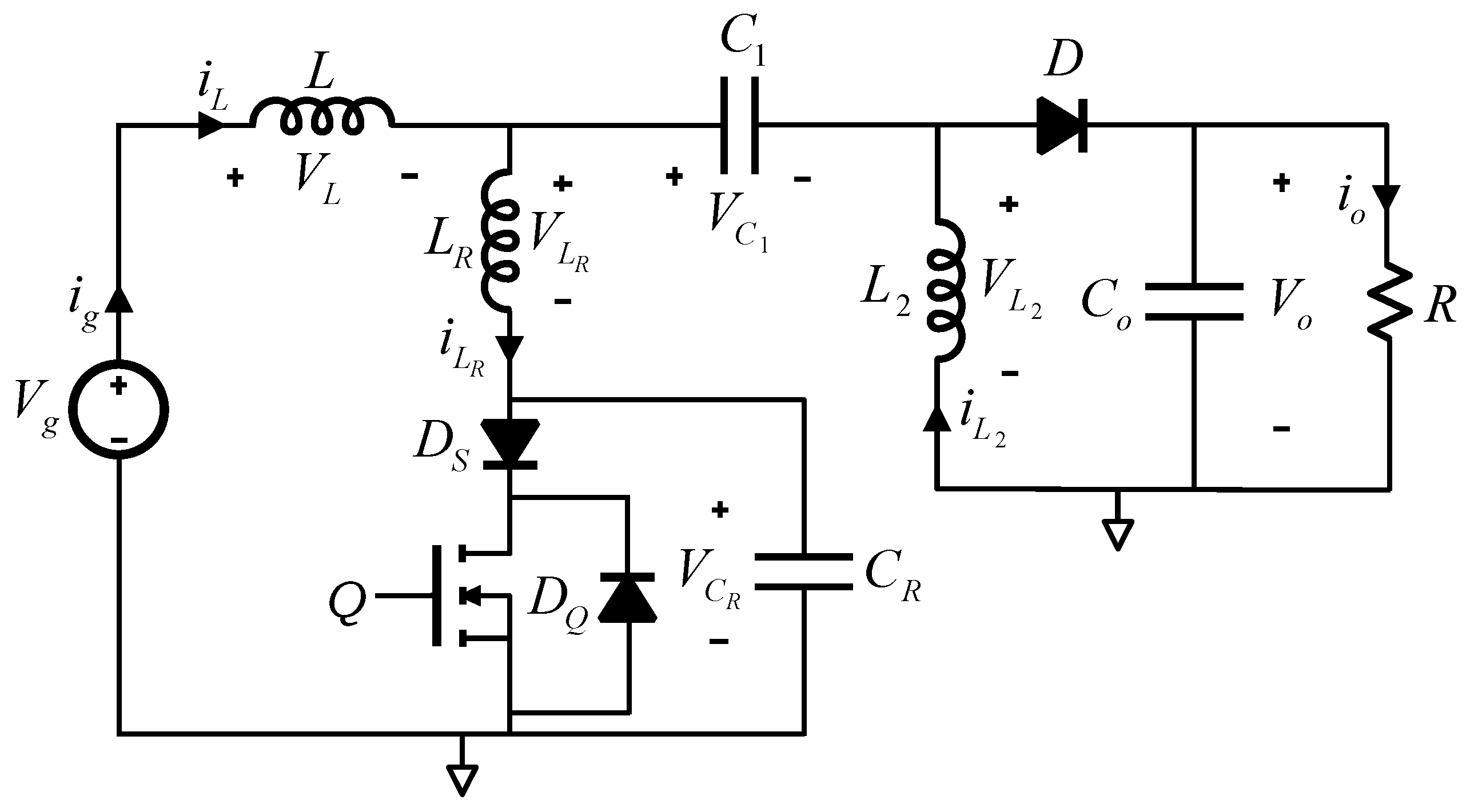
2. Proposed Converter Topology
The proposed configuration consists of the combination of two quasi-resonant ZVS, full-wave, two-inductor converters, Cuk and SEPIC. Both topologies can be combined since they share the same front end. The SEPIC topology provides a positive output voltage, while the Cuk topology is used to obtain a negative output voltage, resulting in two bipolar, symmetrical or dual output voltages. This combination strategy has been described in [
29], operating in hard-switching, while in [
30,
31], it was applied to similar topologies, operating in quasi-resonant half-wave version combination. The combination converter requires only one controllable power switch, which contributes to increasing the power density by using fewer components, being suited for converters up to some hundred watts and keeping continuous input and output currents. Another important advantage is that the proposed combined converter can operate in both step-down and step-up modes, increasing or decreasing the output voltage with respect to the voltage applied at its input. The two output voltages can be regulated by a single controller. There is a wide variety of applications in which converters with symmetrical or dual output (single-input dual-output, SIDO) are used [
32]. The Cuk and SEPIC ZVS QR topologies are shown in
Figure 1 and
Figure 2, respectively. Both are full-wave versions [
12] for ZVS operation.
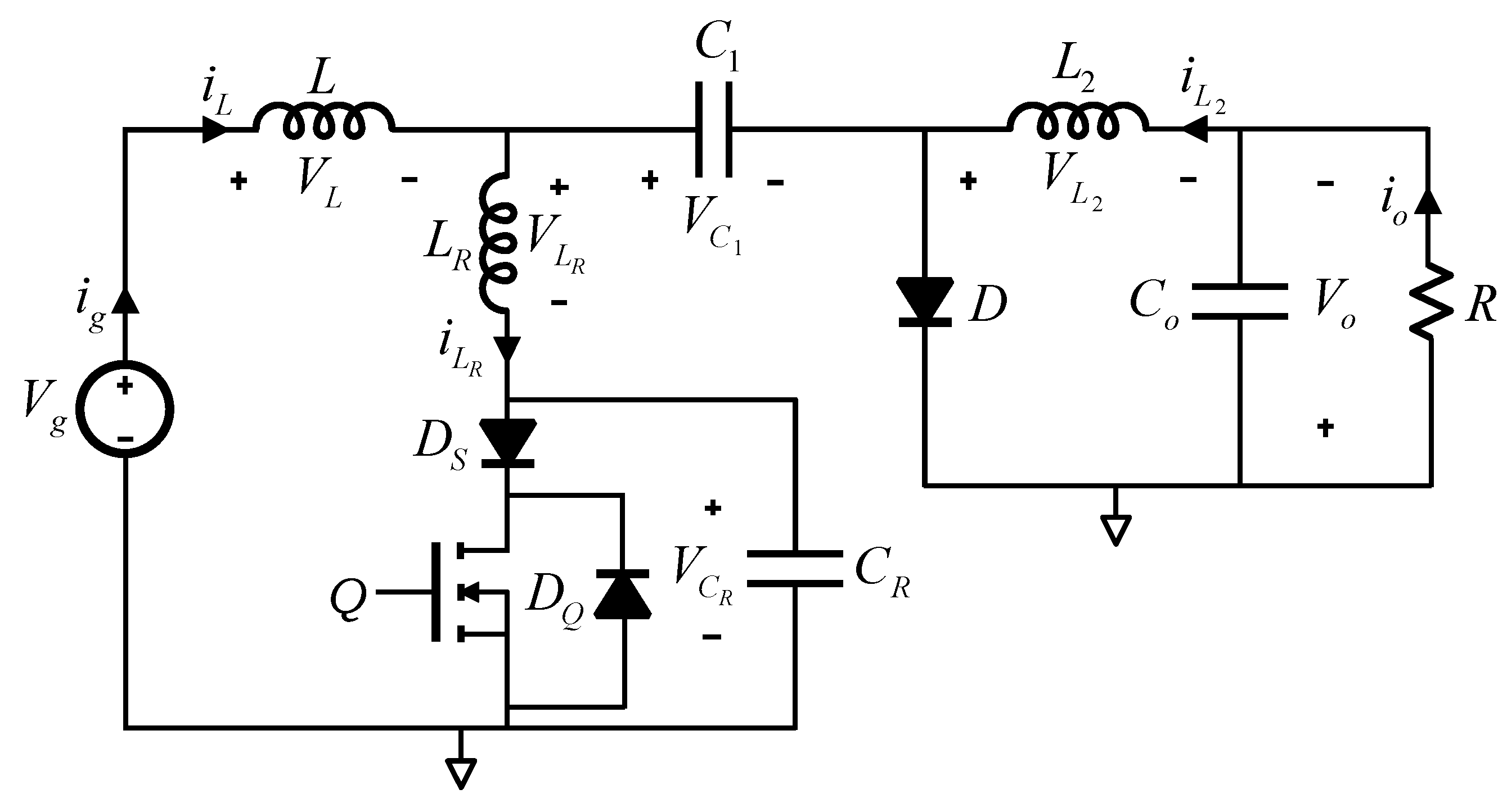
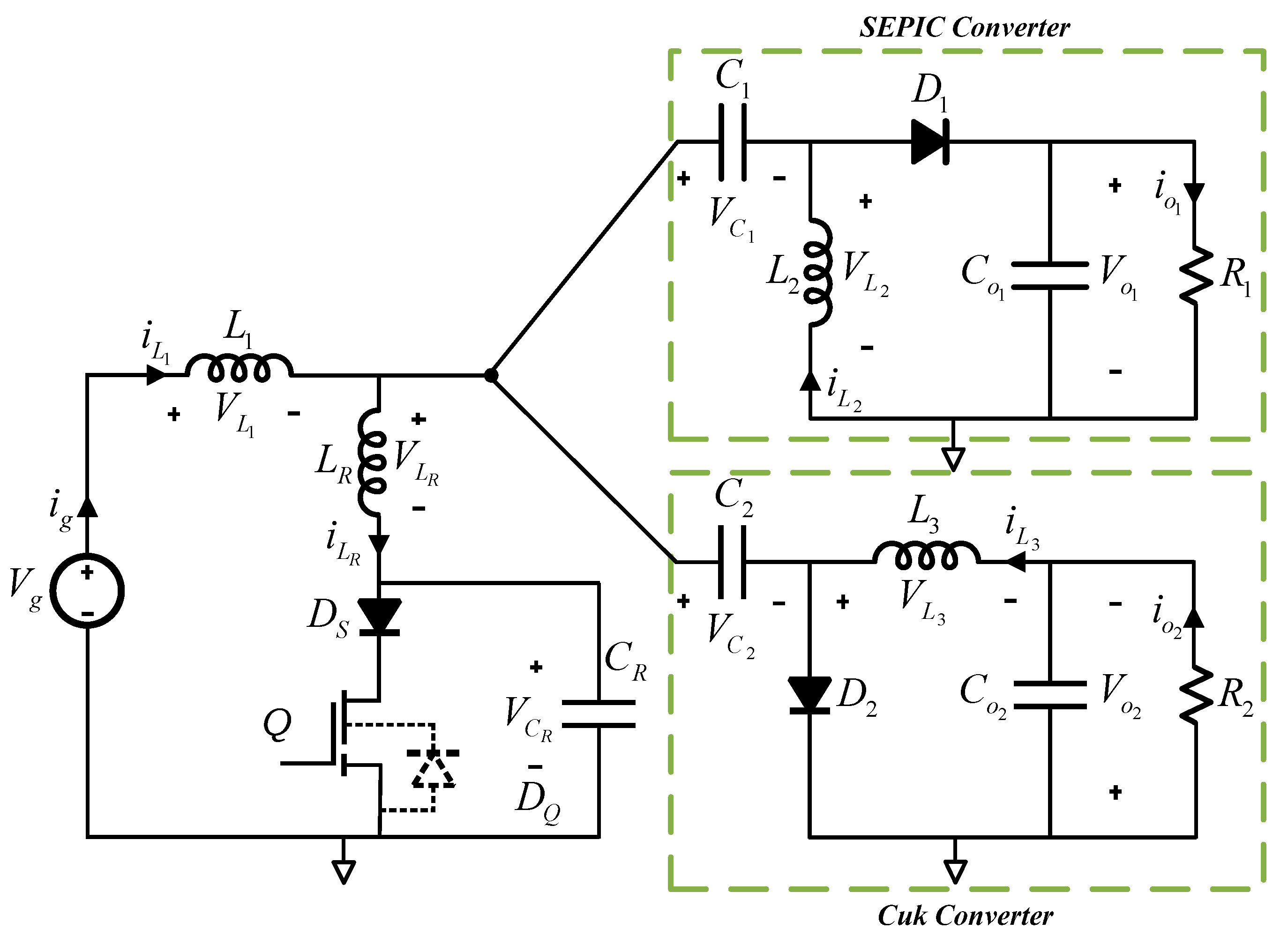
The new proposed configuration, resulting from the combination of Cuk and SEPIC, is shown in
Figure 3, where the input inductor
L1, the power switch
Q and the associated resonant circuit
LR and
CR are shared.
The converter operates in four intervals. Initially, with Q and DS off, the current from the filter inductor flows through the resonant tank (LR–CR), causing CR to charge linearly. When CR reaches the value of Vg + Vo1 or Vg + Vo2, D1 and D2 conduct, supplying current to the loads while CR follows a sinusoidal voltage variation. Once the resonant cycle completes and CR returns to zero (at the end of the negative half-cycle), Q must be turned on to direct current through LR, preventing further resonance. Finally, Q and DS conduct while the freewheeling diodes turn off, restoring initial conditions before the next switching cycle begins, which will start when Q is turned off again.
3. Analysis of SIBSO ZVS QR Cuk–SEPIC and Operating Modes
The analysis of the ZVS QR Cuk–SEPIC full-wave combination converter (
Figure 3) can be performed by dividing the period (
Ts) in four intervals, resulting in four equivalent circuits, showed in
Figure 4,
Figure 5,
Figure 6 and
Figure 7. It is assumed that the currents through filter inductors (
L1,
L2 and
L3) and the capacitor (
C1,
C2,
Co1 and
Co2) voltages stay relatively constant during
Ts.
In addition, the following parameters (Equation (1)) and considerations are taken into account: semiconductors (diodes and GaN FET) are considered ideal (zero voltage drops, zero reverse currents, zero switching times and zero parasitic capacitors).
Assuming full-wave operation with respect to the resonant action, Ds does not allow conduction of the diode associated with the GaN FET (DQ), which causes the voltage across the resonant capacitor to change sign. The analysis begins by assuming the voltage across the resonant capacitor (CR) is zero (the power switch is turned on).
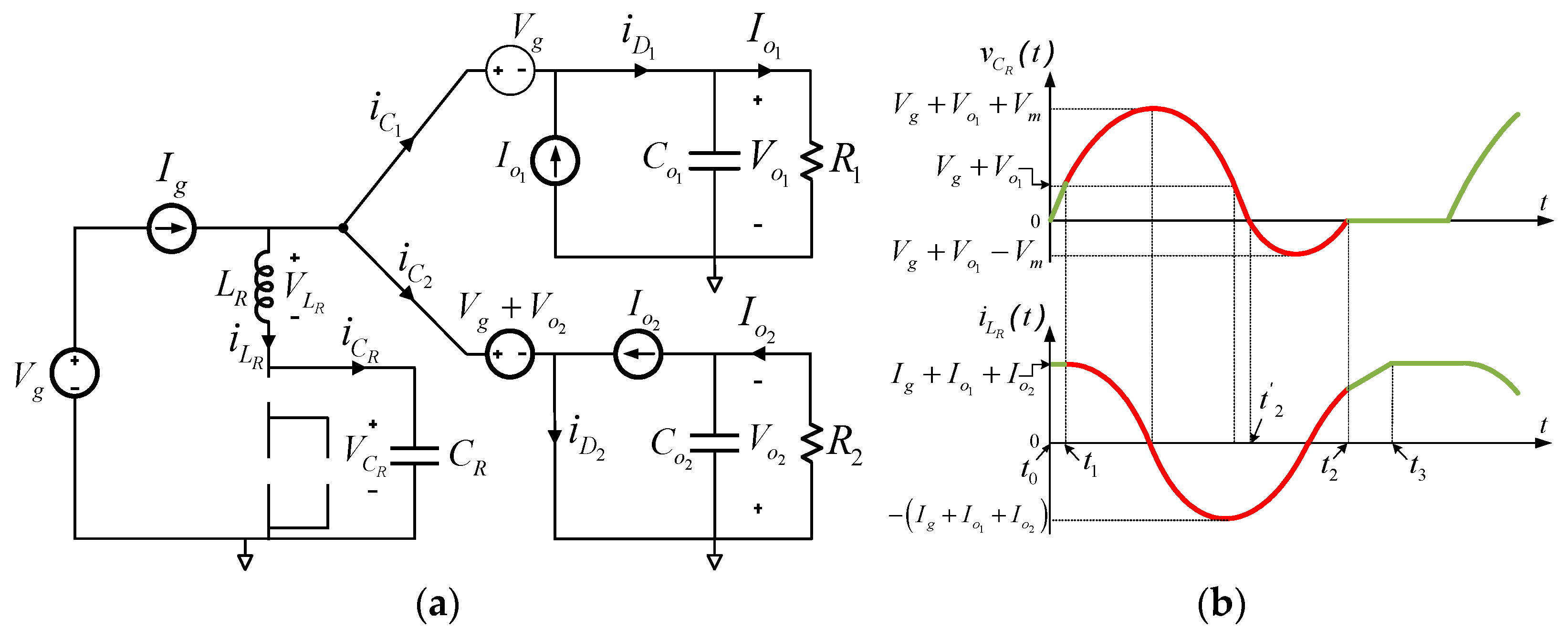
At
t0,
Q and
DS are turned off (
Figure 4). The currents of the filter inductors (
L1,
L2 and
L3) flow through
LR and
CR. The voltage at
CR (and thus also at
Q) grows linearly from zero (ZVS operation). This interval ends when
CR reaches the value of
Vg +
Vo1 or
Vg +
Vo2 and the free-wheeling diodes (
D1 and
D2) become directly biased (
t1).
Figure 4.
Linear stage. (a) Equivalent circuit of the ZVS QR Cuk–SEPIC full-wave combination converter during interval 1 [t1 − t0]. (b) Main resonant waveforms (red: actual interval).
Figure 4.
Linear stage. (a) Equivalent circuit of the ZVS QR Cuk–SEPIC full-wave combination converter during interval 1 [t1 − t0]. (b) Main resonant waveforms (red: actual interval).
The states of the power semiconductors are as follows:
Q, DQ, DS, D1 and D2 off.
The initial conditions are as follows:
From circuit Kirchhoff laws, the following differential equations are obtained (
t1 −
t0):
The interval time duration is:
The diode voltages (
D1 and
D2) are as follows:
- 2.
Interval 2 (Resonant stage) [t2 − t1]:
At
t1, when
CR reaches the value of
Vg +
Vo1, diodes
D1 and
D2 are forward-biased and conduct the current to the loads (
Figure 5). In this situation, the current flowing through
CR and
LR does not follow a linear evolution. The voltage across
CR varies sinusoidally, while the current through
LR varies cosenoidally. The maximum value in
CR reaches (
Vg +
Vo1 +
Vm) in the positive half-cycle, whereas the negative has a minimum value of (
Vg +
Vo1 −
Vm). To analyze this evolution, the interval [
t2 −
t1] is divided into two subintervals [
t′
2 −
t1] and [
t2 −
t′
2], delimited by each half-cycle of the resonant waveform.
Figure 5.
Resonant stage. (a) Equivalent circuit of the ZVS QR Cuk–SEPIC full-wave combination converter during interval 2 [t2 − t1]. (b) Main resonant waveforms (red: actual interval).
Figure 5.
Resonant stage. (a) Equivalent circuit of the ZVS QR Cuk–SEPIC full-wave combination converter during interval 2 [t2 − t1]. (b) Main resonant waveforms (red: actual interval).
The states of the power semiconductors are as follows:
Q, DS and DQ off. D1 and D2 on.
The initial conditions of the subinterval (
t′
2 −
t1) are as follows:
From circuit Kirchhoff laws, the following differential equations are obtained (
t′
2 −
t1):
At
t′
2 the voltage in
CR cross zero, thus:
Initial conditions of the subinterval (
t2 −
t′
2) are as follows:
From circuit Kirchhoff laws, the following differential equations are obtained (
t2 −
t′
2):
At
t2 the voltage in
CR reaches zero again:
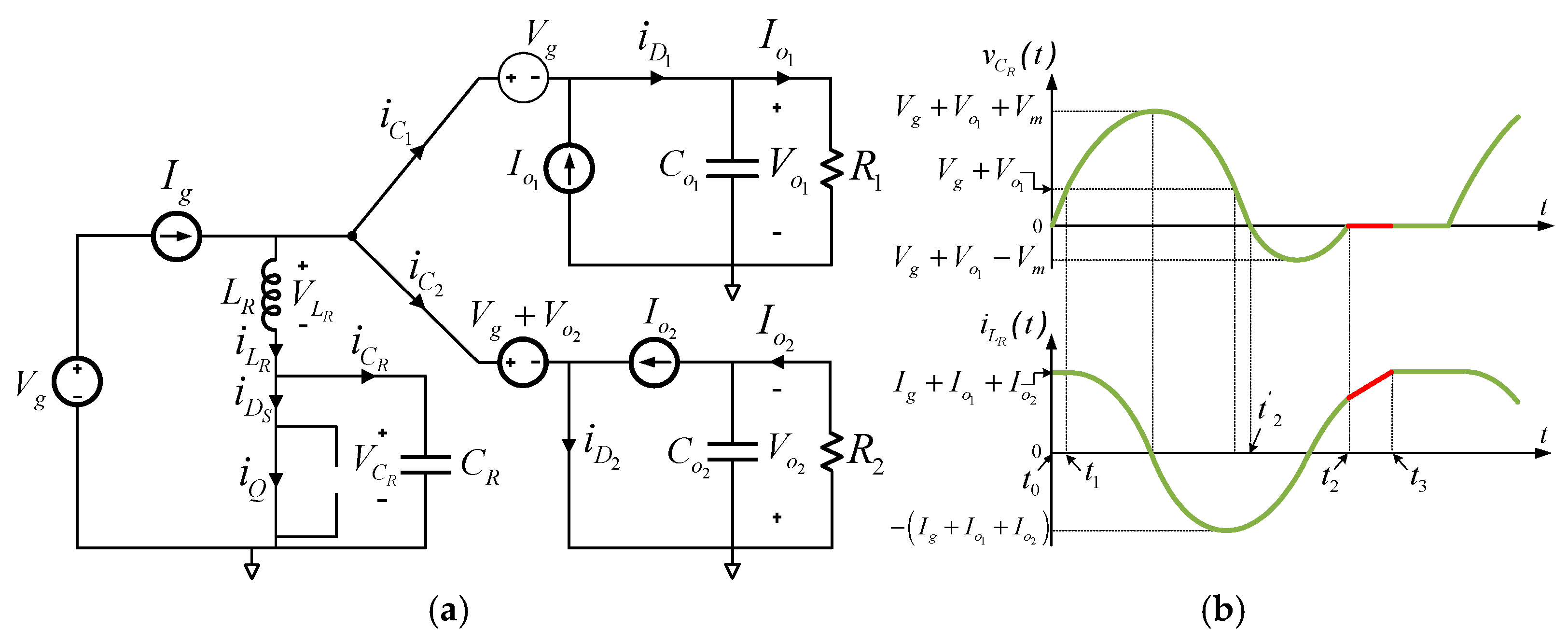
- 3.
Interval 3 (Discharge-inductor stage) [t3 − t2]:
At
t2, the voltage in
CR reaches zero since the resonant full wave has been completed.
Q must already be closed in order to conduct the current (together with
DS) through
LR and prevent it from re-circulating through
CR, avoiding a repetition of the resonant wave (
Figure 6). The interval will end when the free-wheeling diodes are turned off (
t3).
Figure 6.
Discharge-inductor stage. (a) Equivalent circuit of the ZVS QR Cuk–SEPIC full-wave combination converter during interval 3 [t3 − t2]. (b) Main resonant waveforms (red: actual interval).
Figure 6.
Discharge-inductor stage. (a) Equivalent circuit of the ZVS QR Cuk–SEPIC full-wave combination converter during interval 3 [t3 − t2]. (b) Main resonant waveforms (red: actual interval).
The states of the power semiconductors are as follows:
Q, DS, D1 and D2 on. DQ off.
The initial conditions are as follows:
From circuit Kirchhoff laws, the following differential equations are obtained (
t3 −
t2):
The interval time duration is:
- 4.
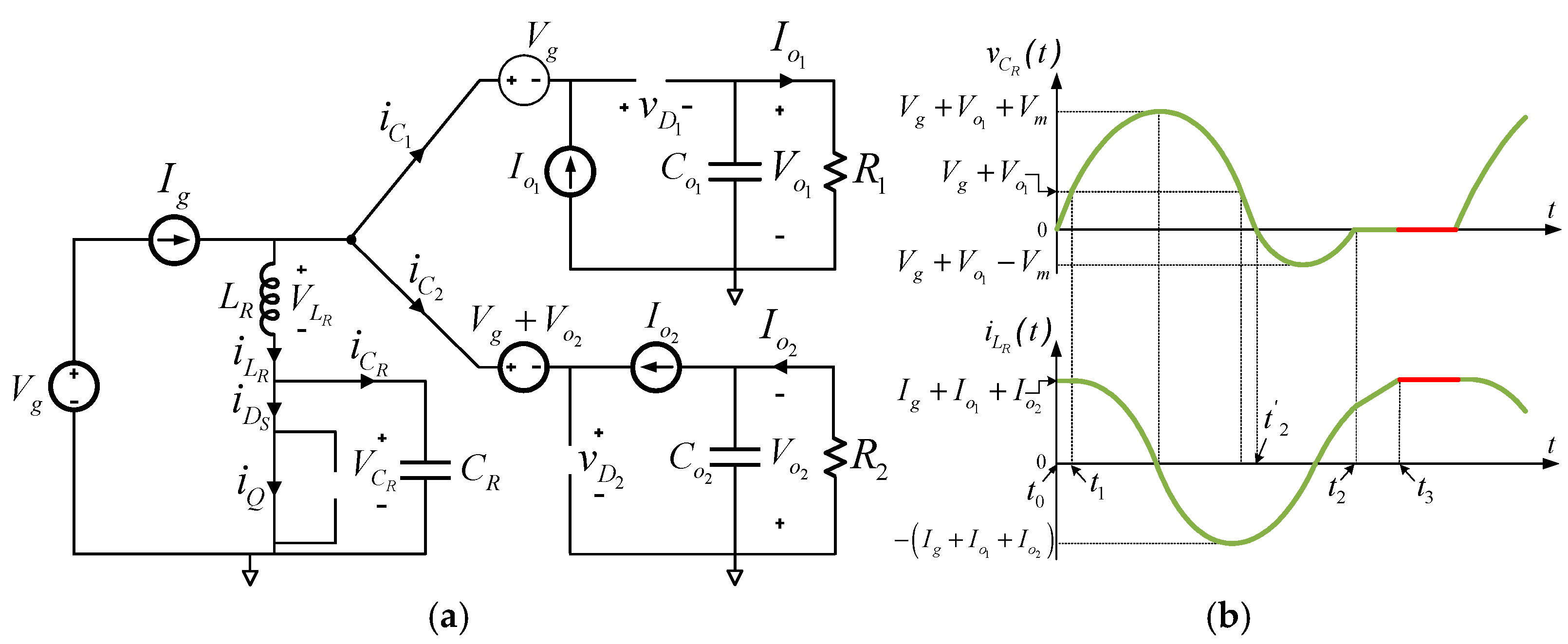
Interval 4 (Passive stage) [Ts − t3]:
At
t3,
Q and
DS are in conduction, while the free-wheeling diodes are reverse-biased (
Figure 7). All the variables reach their initial values for the following period. This interval ends when
Q is turned off, therefore starting a new switching cycle.
Figure 7.
Passive stage. (a) Equivalent circuit of the ZVS QR Cuk–SEPIC full-wave combination converter during interval 4 [Ts − t3]. (b) Main resonant waveforms (red: actual interval).
Figure 7.
Passive stage. (a) Equivalent circuit of the ZVS QR Cuk–SEPIC full-wave combination converter during interval 4 [Ts − t3]. (b) Main resonant waveforms (red: actual interval).
The states of the power semiconductors are as follows:
Q, DS, on. D1, D2 and DQ off.
The initial conditions are as follows:
Figure 8 shows the main waveforms of the proposed converter, as well as their peak values, obtained in the previous analysis. The two symmetrical output voltages can be obtained by considering the average voltage at the free-wheeling diodes (
D1 and
D2) during a period, since these voltages are filtered by the output capacitors (
Co1 and
Co2).
The
VD1 (
t)
VD2 (
t) voltages are given as:
And are given as:
The current conversion relations can be expressed as:
Also, those conversion relations can be expressed by defining the parameter
m as:
5. Simulation Model and Results
In order to verify the ZVS QR Cuk–SEPIC full-wave combined converter analysis; a simulation model has been implemented using Matlab/Simulink R2024b software (Version 24.2 R2024b). The implemented topology is shown in
Figure 3. First, the operation in step-down mode was simulated for an input voltage of 48 V, to obtain a symmetrical output voltage of ±24 V, with a load variation of
R1 and
R2 between 4.7 Ω (245.1 W) and 10 Ω (115.2 W), maintaining the resonant action. For this purpose, the
LR–
CR resonant tank has been dimensioned to satisfy the zero voltage, full-wave condition:
.
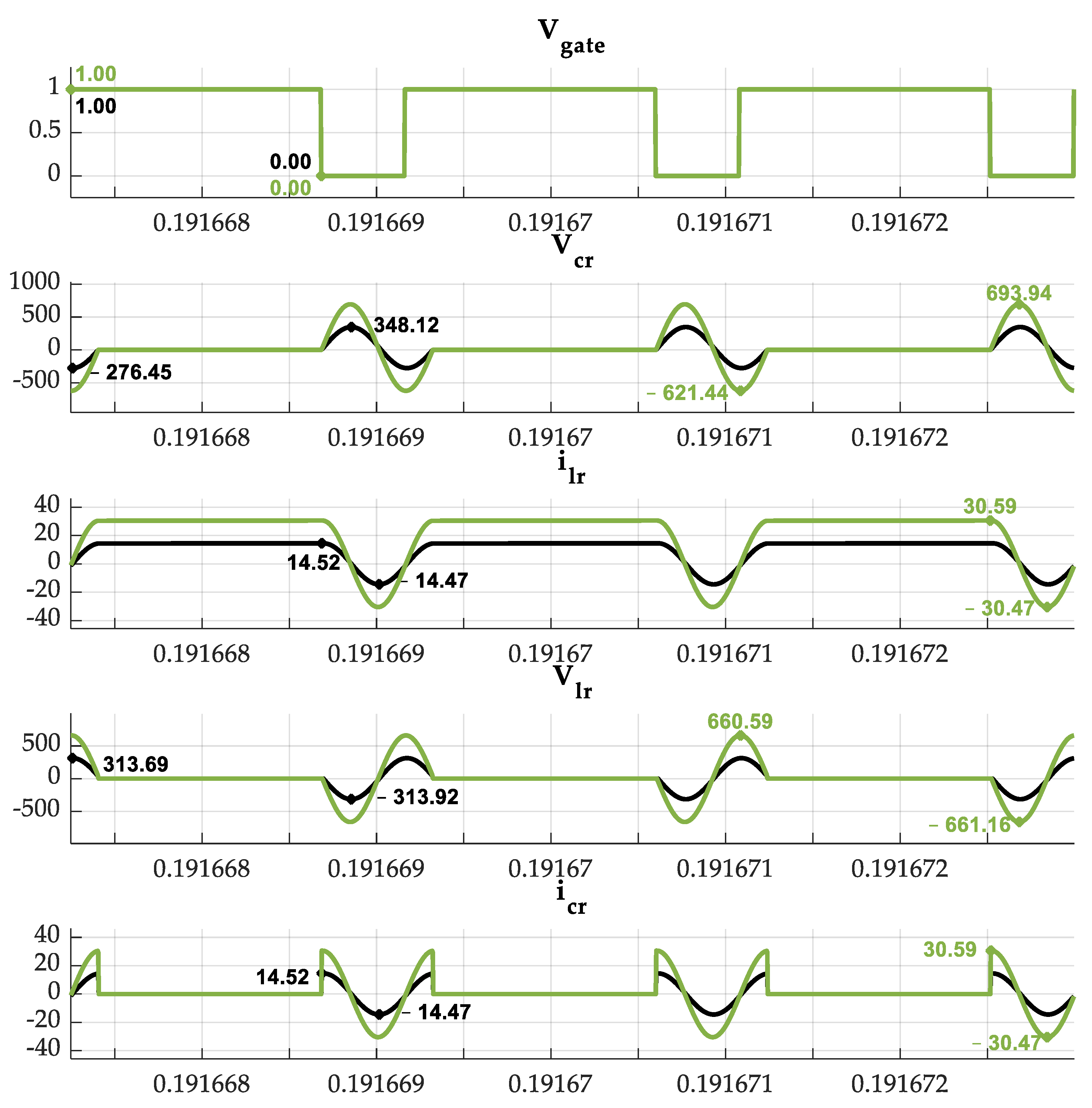
Secondly, the operation in boost mode was simulated for an input voltage of 12 V, obtaining a symmetrical output voltage of ±24 V. In addition, the model was subjected to the same load variations, also between 4.7 Ω (245.1 W) and 10 Ω (115.2 W). The simulation results obtained are shown in
Figure 9 and
Figure 10. These results reproduce and confirm the previous analysis, whose waveforms are shown in
Figure 8. The model was simulated with the parameters provided in
Table 1, in step-down mode, setting the operating frequency at 1.044 MHz, with a minimum
off-time of 331 ns and in step-up mode, at a frequency of 521.72 kHz, with a minimum
off-time of 364 ns. In both cases, to achieve the resonant action,
.
From the theoretical analysis and from the maximum and minimum values showed in
Figure 8, the peak voltage in the resonant capacitor at 115 W (10 Ω) can be estimated to reach the maximum value as
= 227.77 V and the minimum value as
= −83.77 V. The simulated maximum and minimum values (
Figure 9) are 228.43 V and −83.14 V, respectively, with a 0.3% error (0.66 V). The remaining maximum and minimum simulated values were compared with the theoretical values, shown in
Figure 8, providing relative differences of less than 1%.
6. Loss Estimation Model of the Combined SIBSO Converter
In order to simulate the operation of the converter in “non-ideal” conditions and estimate its efficiency, parasitic components have been added to the simulation model, such as voltage drop in the diodes, conduction resistance of the GaN FET, series resistors of all inductors and capacitors (ESR) and parallel resistors of the filter inductors (EPR). In the background, we aim to perform a loss analysis and estimation that, by considering the RMS current analysis for each component and the involved non-idealities, allows us to estimate the losses in the components involved in the combined SIBSO converter. A theoretical analysis of this estimation can be found in references [
33,
34,
35]. The values considered are those provided in the technical datasheets by the manufacturers, for the components summarized in
Table 2. A model in Matlab/Simulink has been implemented in order to estimate each component’s losses and the converter efficiency.
First, the model was simulated with ideal components, obtaining an efficiency reaching 100%. Then, each of the non-idealities of each component considered were added one by one, and finally, all of them were simulated together. In addition, the conventional hard-switching converter (without a resonant tank) has also been simulated using the same parasitic values as in the model with soft-switching.
To take into account the loss due to hard-switching, a snubber network has been added to the main switch, calculating the values for RS and CS as a function of the parameters Eon (turn on switching energy) and Eoff (turn off switching energy) provided by the manufacturer.
These results are shown in
Figure 11, where the influence of each component on the efficiency of the converter, individually and overall, is analyzed. Furthermore, the advantage of the proposed converter (green line) is verified, as the losses of the conventional converter (black line) would be much higher due to hard-switching losses at 1 MHz. As a result, to obtain losses similar to the resonant converters, the operating frequency must be lowered to 80 kHz.
Figure 12 shows the percentage distribution of losses in each component for the same conditions.
Although the above simulations have been performed for a voltage conversion ratio of 0.5 (
m = 2/3) mainly to show high-frequency operation, the converter can also operate at other conversion ratios, so in
Figure 13, a frequency sweep between 500 kHz and 1 MHz is performed, operating the converter in both step-up and step-down modes and measuring the efficiency and output voltage. The input voltage is set at 48 V, while the output voltage changes between 22 and 80 V (voltage conversion ratio of 1.5,
m = 2/5) and the efficiency varies between 92 and 82%.
7. Experimental Results
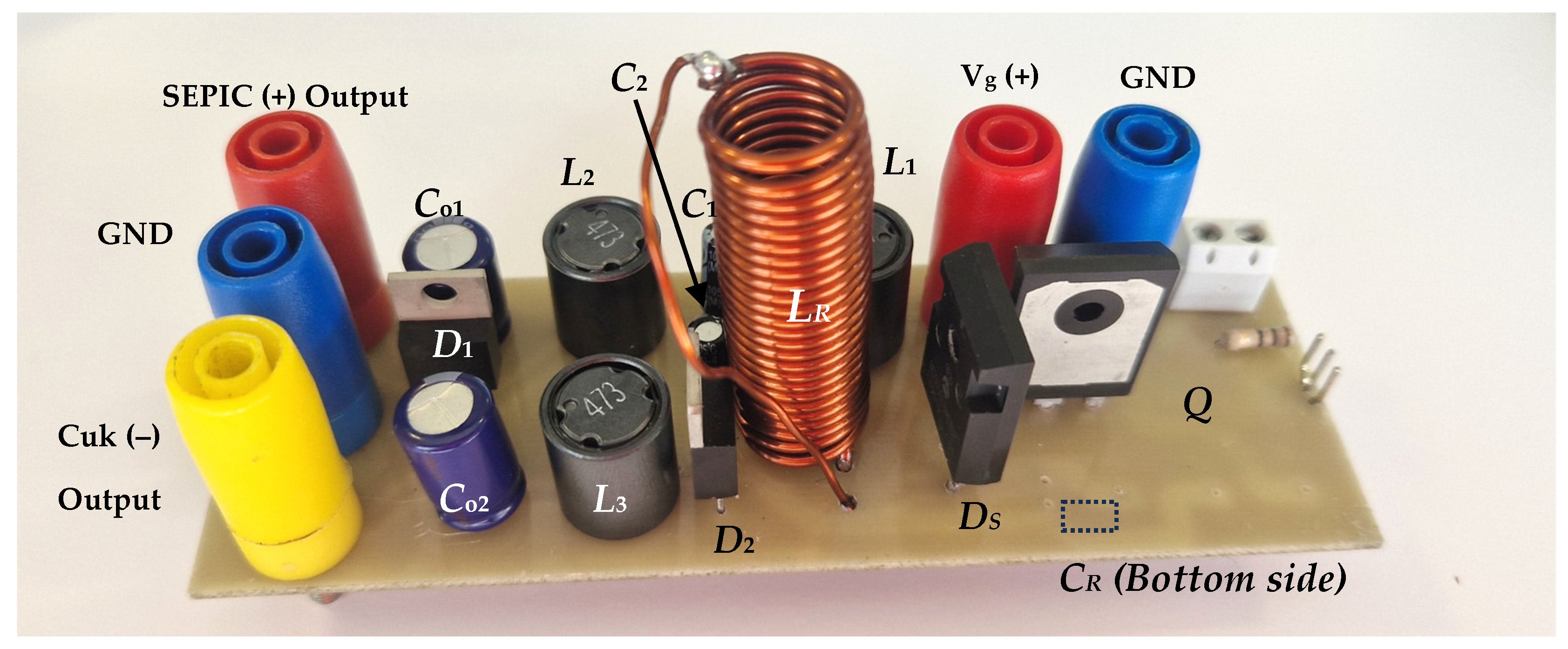
In order to verify the previous analysis and simulation results, an experimental prototype based on the configuration proposed in this work has been implemented, which is shown in
Figure 14. The most relevant waveforms have been measured, mainly those related to resonant operation, also verifying that soft-switching at zero voltage occurred.
The prototype was tested in an open-loop configuration, using the UCC5304DWV driver specifically engineered for GaN FETs. In addition, a GaN FET was employed as the main switching element, enhancing low-loss and high-frequency performance. This open-loop setup enabled an isolated evaluation of the converter response and allowed for a detailed analysis of the more relevant resonant waveforms. The integration of the UCC5304DWV driver with a GaN FET enabled precise control over the switching operation, ensuring optimal performance and minimizing losses before the implementation of closed-loop control strategies. The gate signal was generated digitally by using an ESP32 microcontroller.
7.1. Operational Parameters of the Proposed Converter
The prototype operates using a specific set of components and is designed to work within predefined parameters to ensure optimal operation. Key components include capacitors and inductors precise values, especially for the resonant tank, customized to the circuit’s requirements, as well as gate driver and semiconductor devices. The prototype is designed to operate with a voltage conversion ratio of
V for an output power of 144 W (72 W in each output). A summary of the components used and the parameters of the converter is provided in
Table 3. This table shows specifications, including the selected semiconductor devices, passive components, and most relevant parameters.
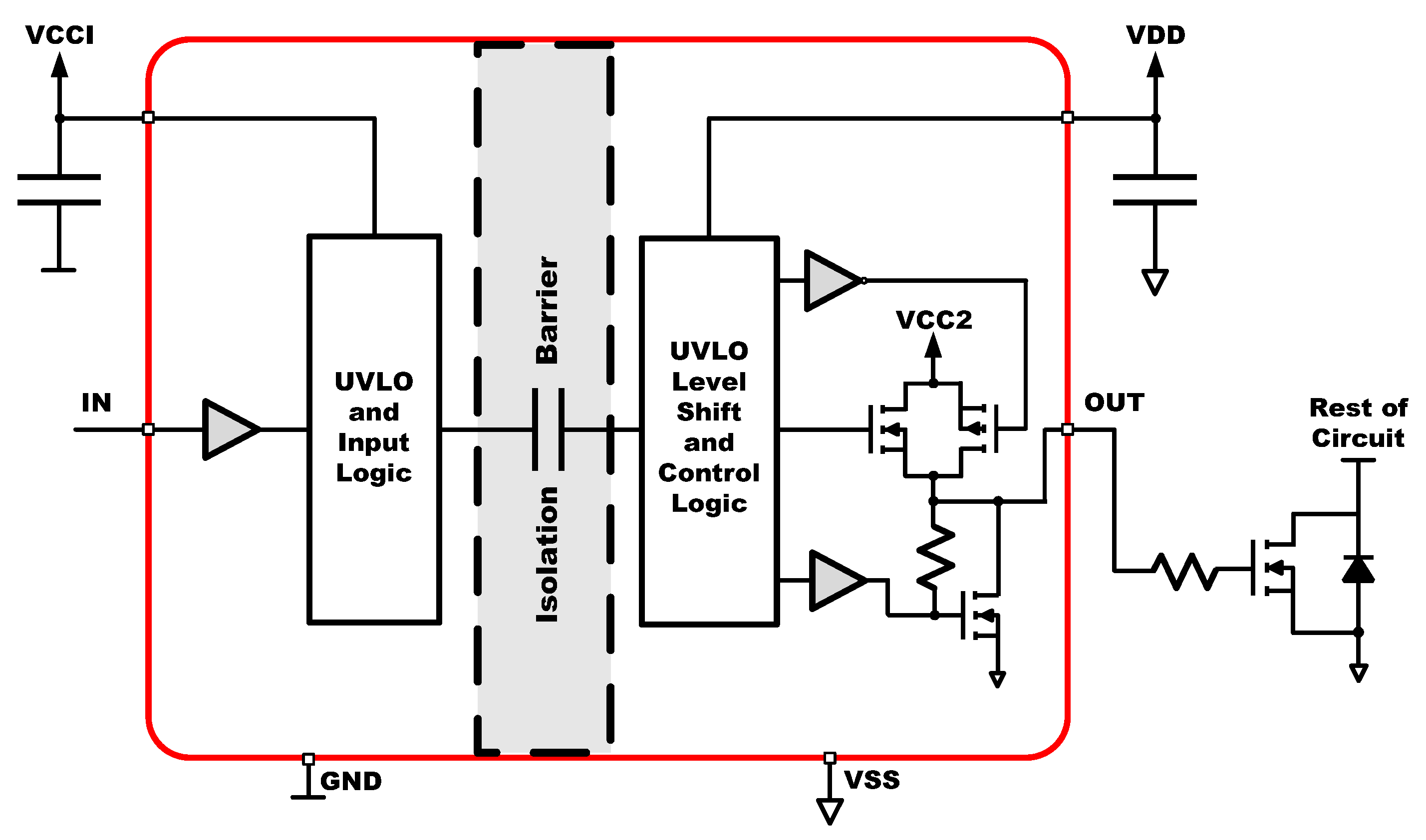
7.2. Gate Drive Circuit Overview
The UCC5304 is an isolated gate driver designed to control power transistors like MOSFETs or GaN FETs, ensuring safe operation through a galvanic isolation barrier. The driver receives a control signal at the IN pin, processed by the under voltage detector UVLO and input logic block, which ensures proper operation only when the input voltage is within the required range. The processed signal crosses the isolation barrier and is received by the level shift and control logic, which drives the totem pole output stage. This output stage provides the necessary gate drive current at the OUT pin to switch the external power transistor efficiently. The UCC5304 is particularly suited for GaN FETs in high-frequency applications, where fast switching is essential for performance and efficiency. A diagram block of this driver is shown in
Figure 15. All the data related to the driver are available in [
36]
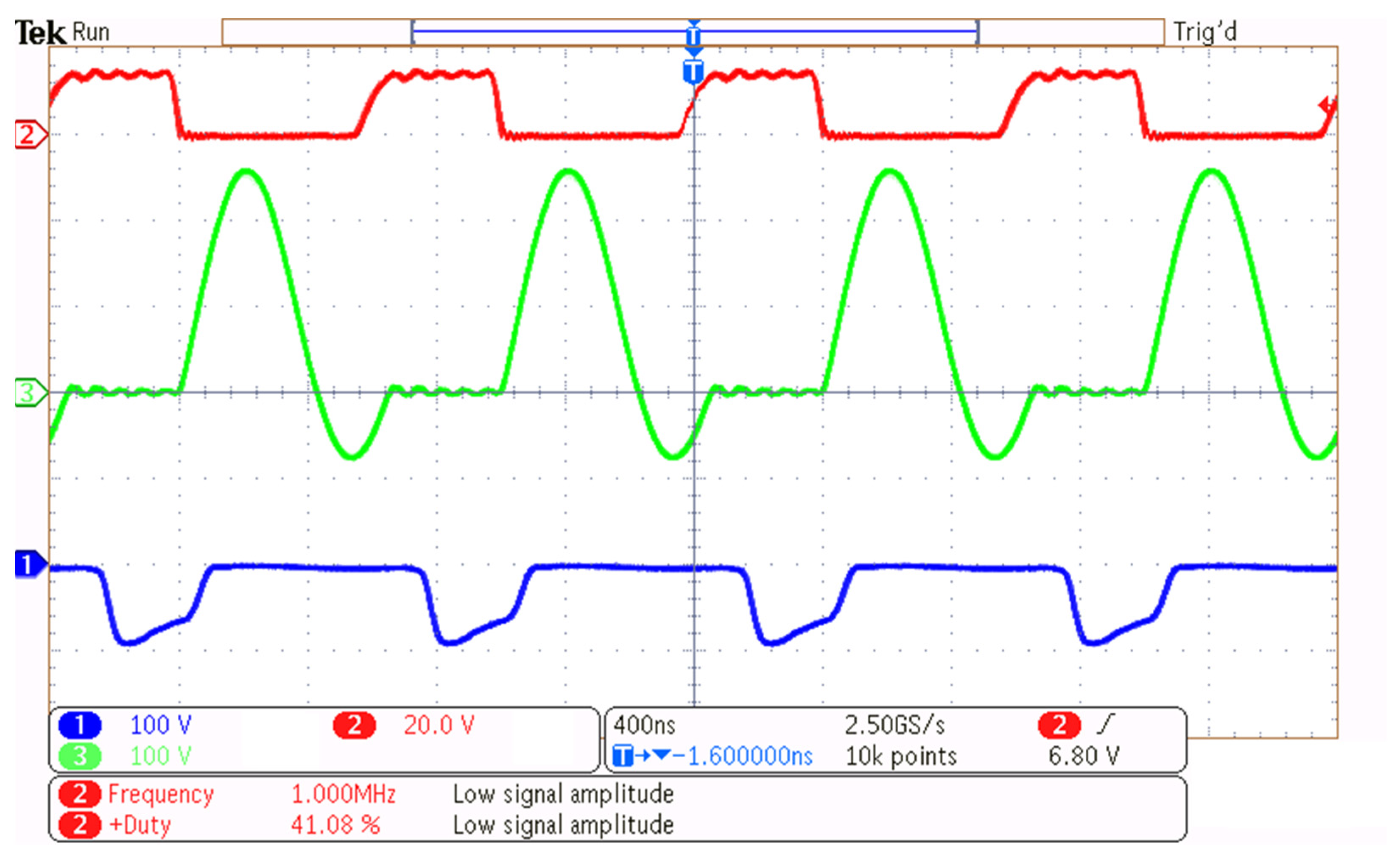
7.3. Main Waveforms of the ZVS QR Cuk–SEPIC Full-Wave Combination Converter
The main resonant waveforms,
and
, are shown in
Figure 16 as well as the main switch excitation signal
. These experimental waveforms of the quasi-resonant converter operating under zero-voltage switching (ZVS) conditions confirm the expected resonant behavior. When the switching device turns off, the energy stored in the resonant inductor transfers to the resonant capacitor, causing the capacitor voltage to rise in a nearly sinusoidal form. This oscillation continues as the voltage develops a full positive half-cycle, ensuring that sufficient time is allowed for the resonant action to occur (
Figure 8). The GaN switch must turn on at any point during the negative half-cycle of the resonant capacitor voltage and before this half-cycle ends, allowing the inductor to fully charge. The cycle repeats when the switch turn off again. It can be seen that the maximum value of the voltage at the resonant capacitor reaches the value of 260 V, which theoretically should be 266.72 V.
Figure 17 contains two pictures displaying the experimental results of the prototype converter. In both, the setup includes the converter, an oscilloscope measuring the resonant capacitor voltage along with the input current, and two multimeters measuring the output voltages. In
Figure 17a, the converter is operating at a frequency of 1 MHz to provide a bipolar output voltage of ±24 V, while in
Figure 17b, it is set at 1.26 MHz to deliver ±12 V. It can be seen how the second case has nearly no negative half-cycle, as it is at conditions close to the resonance limit.
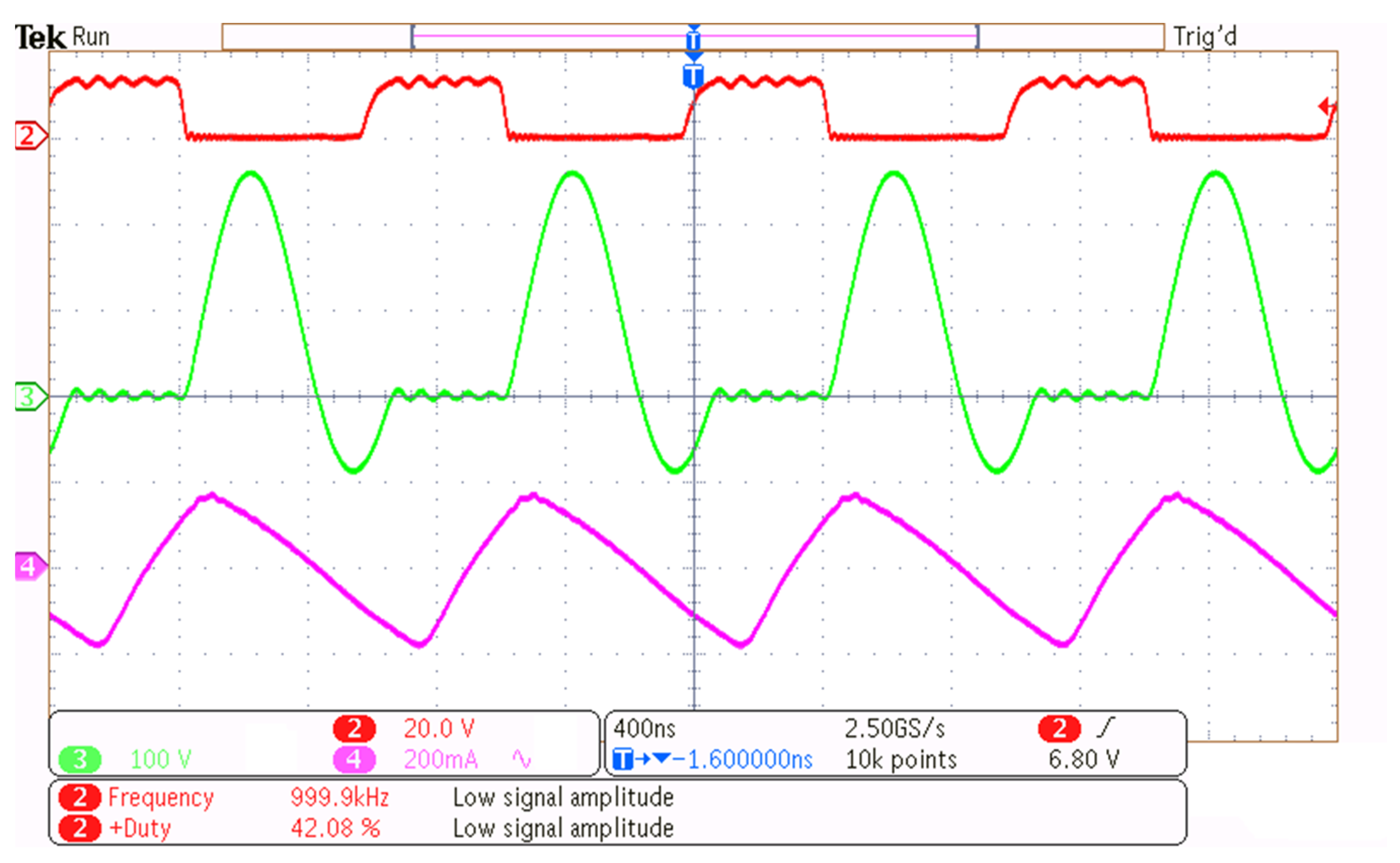
In the experimental results shown in
Figure 18, a small parasitic high-frequency oscillation in the inductor voltage waveform is observed during the interval where it is theoretically expected to remain at zero. This deviation from the ideal response is due to parasitic elements in the circuit, such as parasitic capacitances in the diodes. Despite these imperfections, the overall waveform confirms that the expected resonant action develops. The maximum inductor voltage amplitude varies with operating frequency and load conditions, demonstrating the characteristic behavior of quasi-resonant operation, where higher switching frequencies result in shorter resonant periods and faster voltage transitions. The resonant inductor voltage follows a behavior complementary to the voltage on the resonant capacitor, with polarity inverts corresponding to the oscillatory charging and discharging of the capacitor.
The voltage in the diodes shows some deviation in comparison to the ideal waveform, as the negative value should remain constant. This deviation, which can be observed in
Figure 19, is due to the parasitic capacitance of the diodes, although the resulting waveform is similar to the expected behavior and does not affect their function.
7.4. Ripple Characteristics
Figure 20 displays the bipolar output voltages, illustrating the symmetrical behavior of the converter. The waveform confirms that the converter generates balanced positive and negative output voltages, maintaining the expected voltage levels. The measured output voltage ripple is also presented in
Figure 21.
Meanwhile,
Figure 22 shows the input current ripple, which reflects the switching behavior and the effectiveness of the input filtering stage. Controlling the input current ripple is crucial for minimizing electromagnetic interference (EMI). Furthermore, the waveform in
Figure 22 confirms that the inductor core operates below saturation, developing the expected waveform.
Figure 23 shows the output inductor’s current ripple of the ZVS QR Cuk–SEPIC full-wave combination converter. Trace (a) corresponds to the SEPIC output current, while (b) represents the Cuk output current, highlighting its respective ripple characteristics.
7.5. Dynamic Response and Stability
To analyze the dynamic response of the converter, the prototype was subjected to variations in both load and input voltage. These tests were designed to assess the converter’s behavior under different operating conditions, providing valuable insights into its transient performance. Key parameters, such as output voltage and resonant capacitor voltage, were measured to evaluate the system’s response to these variations.
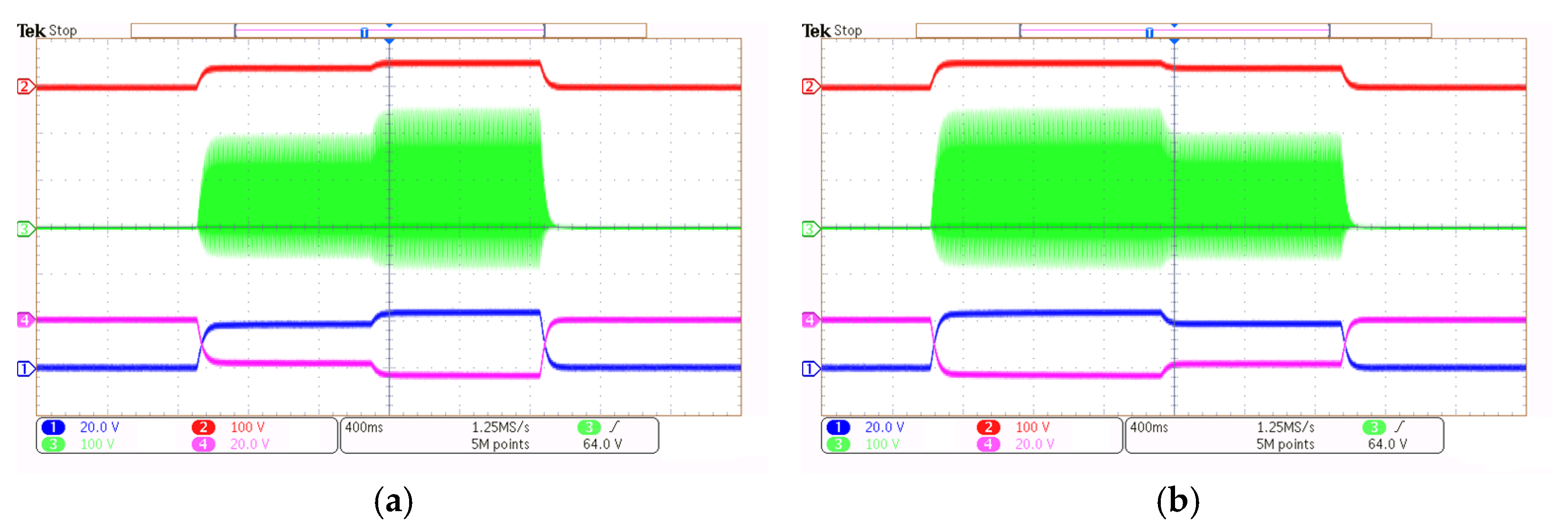
Figure 24 illustrates the dynamic response of the converter when subjected to a 50% load variation. The experiment follows a sequential process: first, the converter is powered on; then, the load variation is introduced; and finally, the converter is turned off. As shown in the figure, the SEPIC and Cuk output voltages (CH 1 and CH 4) exhibit transient behavior in response to the load change, while the resonant capacitor voltage (CH 3) adapts accordingly. The two scenarios presented correspond to an increasing load from 10 Ω to 5 Ω (a) and a decreasing load (b) from 5 Ω to 10 Ω.
Figure 25 presents the response of the converter when subjected to a 20% variation in input voltage. The procedure consists of powering on the converter, applying the input voltage change, and subsequently turning it off. The SEPIC and Cuk output voltages (CH 1 and CH 4) adjust to the variation, while the resonant capacitor voltage (CH 3) reflects the transient effects. The figure displays two cases: (a) increasing input voltage from 38 to 48 V and (b) decreasing input voltage from 48 to 38 V.
7.6. Thermal Response
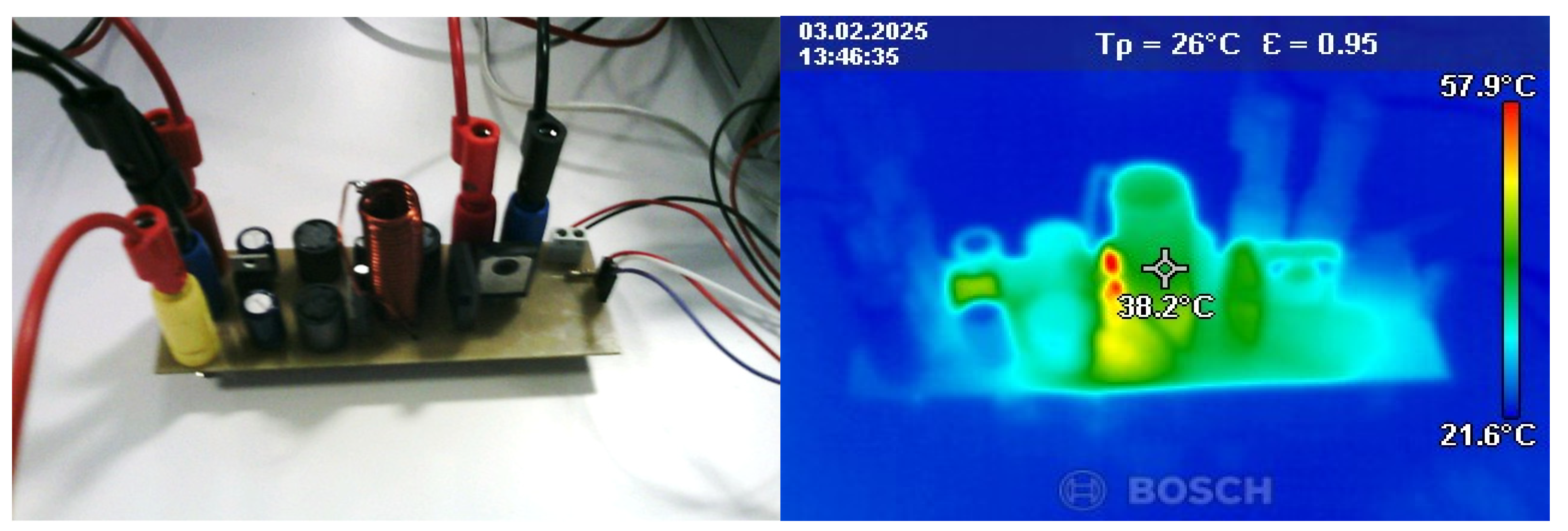
To understand the thermal distribution of the converter, a thermal camera was used to capture and analyze the temperature variations in all components of the converter. This made it possible to identify possible overheated regions and to evaluate the thermal response. The thermographic images of the experimental prototype under operation shown in
Figure 26 reveal that the components experiencing the highest temperature rise are the diodes and the resonant inductors. No heat sinks have been used in the prototype.
Diodes exhibit significant heating due to their switching and conduction losses, which are inherent to the quasi-resonant operation of the converter. The resonant inductor also shows considerable temperature rise due to the high RMS currents flowing through it. These currents increase conduction losses, which are increased by the inductor’s equivalent series resistance (ESR). The ESR results from the use of an air-core inductor, which is necessary to minimize core losses at high switching frequencies. In contrast, the gallium nitride (GaN) device remains notably cooler than the other components, attributed to the implementation of soft-switching, which minimizes switching losses and reduces the total power dissipation. The combination of GaN FET technology and quasi-resonant operation enhances the converter’s efficiency, as lower energy is lost as heat, leading to improved thermal response.
Figure 27 and
Figure 28 show the converter placed next to the load resistors. This setup allows for a direct comparison of the temperature distribution between the converter and the resistive loads. The image clearly illustrates the thermal gradient, with the load resistors reaching much higher temperatures due to their function as power-dissipating elements. This contrast highlights the power distribution of the converter, as its core components maintain relatively lower temperatures, further supporting the benefits of GaN-based designs in reducing thermal management.
7.7. SIBSO DC–DC Converter Efficiency
The method to estimate the efficiency has been the measurement of the average values of the voltage Vg and current across the inductor L1. With the product of these values, the input power was obtained. To calculate the output power, the output voltage was measured at each of the outputs, as well as the current through each of the loads. The voltage–current product was calculated for each output and then the sum of the two was added together to obtain the output power. Finally, the average measured efficiency, calculated as the ratio between output and input power, was 89.2%. For the voltage and current measurements, Fluke 179 multimeters were used, taking ten samples for each measurement and then considering the average.
The experimental prototype shows similar results to the simulated one, with differences due to the non-idealities of the components, such as parasitic capacitances and inductances, which slightly modify the expected waveforms. However, the results obtained show a good approximation to the waveforms of the simulated model with parasitic components, as well as in the maximum/minimum values. It should be taken into account that is not exactly the same, since the simulation model has taken into account the most relevant parasitic components, but not consider, for example, the parasitic capacitances associated with the diodes, which causes the deviation that can be seen in
Figure 18 and
Figure 19. Although this value can be approximated, it is a dynamic value that depends on the operating point of the component, so it is not easy to obtain an exact value. However, this does not significantly affect the converter operation, so it is assumed in order to compare the difference with the theoretical result, which, as can be seen in
Figure 8, presents a minimal difference. This section concludes with a comparative table of other multiple-output topologies, which is attached in
Table 4.
The proposed SIBSO DC-DC GaN FET converter offers a balance between efficiency, component count, and power density when compared to other state-of-the-art designs. With a power density of 44.3 W/in
3, it ranks second among the listed references, notably below [
35], which reports 150 W/in
3, but higher than others such as [
37] (10.5 W/in
3) and [
39] (7.4 W/in
3). It operates at 1 MHz, matching [
35,
38], which supports compact passive components and improved transient response. In terms of components, this design uses a single, ground-referenced switch, which is the same as [
34,
37], and better than [
35,
37,
38], indicating a simpler control stage. However, the SIBSO proposed topology requires three diodes, slightly more than most references that use just two [
34,
35,
37,
38]. With respect to filter components, it uses four capacitors and three inductors, which is on par with or only slightly above several other implementations.
Regarding efficiency, this SIBSO converter reaches 89.2%, placing it above [
34,
37], and [
38], but below [
35] (94.6%) and [
39] (92%). Overall, while the proposed SIBSO design does not exceed all references in every metric, it presents a well-rounded solution with high switching frequency, good efficiency, and good power density, supported by a relatively simple switching structure—making it suitable for compact, medium-power applications where soft-switching and integration are priorities.
In terms of costs, the proposed converter offers a cost-effective design by using a single, ground-referenced switch, which reduces the need for complex gate drivers and simplifies control. Additionally, its high switching frequency (1 MHz) enables the use of smaller, lower-value passive components, potentially reducing overall cost compared to lower-frequency designs like [
34,
37]. Regarding power density (44.3 W/in
3), while significantly higher than [
37] (10.5 W/in
3) and [
39] (7.4 W/in
3), it remains below [
35] (150 W/in
3).
8. Conclusions
This paper proposed a new ZVS QR Cuk–SEPIC full-wave combination converter with bipolar output (SIBSO). An analysis of the operating principle of the converter was presented, followed by detailed simulations to show its operation principles under various conditions. A simulation model was also implemented for efficiency estimation, which provides valid data on the behavior and efficiency of the converter. Besides some drawbacks, like the ability to provide electrical isolation and increased voltage and current stress on the switching devices and passive components due to the addition of the resonant tank, which impairs the topology in high-voltage applications, the full-wave quasi-resonant SEPIC-Cuk topology simulation model results were fitted to experimental results, validating its accuracy and providing a tool for further optimizations. The converter operated at a switching frequency of 1 MHz, achieving an output power of around 150 W with an efficiency close to 90%. These results demonstrate the potential of the SIBSO converter for low-voltage bipolar applications, where both efficiency and compactness are critical. Experimental validation was carried out in an open loop, confirming the theoretical predictions, and showing a good alignment between simulation and experimental results. Additionally, thermal response tests showed that the converter operates without significant temperature rise under typical conditions, indicating effective thermal management. The proposed topology shows interesting power densities and efficiencies combining traditional Cuk and SEPIC topologies with only a resonant tank in the power switch to ensure ZVS full-wave at around 1 MHz. This work provides a transformerless, symmetric bipolar output solution capable of operating in both step-down and step-up modes with a limited number of components. Regarding the proposed closed-loop control, the resonant tank hardens the design of the control strategy, as the modulator must be operated at a constant turn-off time. The next work is to design suitable modulators and feedback controllers, together with testing the stability and transient behavior of the obtained solutions when using variable electronic loads with input inductive capacitive filtering.


