1. Introduction
A model of Mealy finite state machine (FSM) [
1] represents the behavior of sequential devices [
2,
3]. In this case, the synthesis of a sequential device is reduced to the synthesis of an FSM circuit. In this paper, we discuss a case when field-programmable gate arrays (FPGAs) [
4] are used for implementing FSM circuits. This choice is determined by the fact that FPGAs are widely used for the implementation of digital systems of varying complexity [
5]. The development of new FPGA-oriented design methods makes sense because, according to experts [
6], they will be widely used in the next few decades.
The FPGA-based design is associated with the need to solve a number of interrelated optimization problems. Most often, it is necessary to obtain a circuit in which either the number of used internal resources, or performance, or power consumption is optimal [
7,
8,
9,
10]. We discuss the case when the dominant optimization problem is the increase of performance (the increasing FSM operating frequency). To implement a Mealy FSM circuit, the following FPGA internal resources are used: look-up table (LUT) elements combined with flip-flops, internal multiplexers, synchronization tree, programmable interconnections and input–outputs [
11,
12,
13]. As the starting object, we chose Mealy FSMs in whose states are encoded by composite state codes (CSCs) [
14]. Using CMCs is based on creating classes of compatible states. Both classes and states are encoded with a minimum number of bits. We propose a method for improving performance that does not lead to a significant overhead (the LUT count and consumed power). The required chip area is estimated as the LUT count [
15].
Currently, there is an increasing amount of information processed by various digital systems [
16]. This requires increasing the system performance. For example, this issue is very important for real-time embedded systems [
17,
18,
19,
20]. Very often, the performance of the digital system becomes one of the decisive factors of commercial success. This is perfectly true for various FPGA-based systems. In the case of FPGA-based systems, it is very important to increase the system performance without a significant overhead [
7]. The overhead may be represented by an increased number of LUTs and interconnections or increased power consumption [
7]. Very often, FSMs are used as a control unit of a digital system. Such FSMs generate control signals in each cycle of the system operation. Obviously, the cycle time of this control FSM significantly affects the performance of the controlled digital system [
21].
Increasing the performance of FSMs is possible due to a state assignment allowing to diminish the number of logical levels in the FPGA-based FSM circuit [
7,
22]. In our current paper, we propose a state assignment method allowing to decrease the FSM cycle time without the significant overhead in internal resources (LUTs, flip-flops, interconnections). The need to solve the related problem is a motivation of our current research.
The main contribution of this paper is a novel method improving the temporal characteristics of LUT-based Mealy FSM circuits with CSCs. The improvement is based on the use of one-hot codes (OHCs) for encoding classes of compatible states. For encoding the compatible states, the maximum binary codes (MBCs) are used. This approach leads to an FSM circuit architecture that is different from the architecture where OHCs are not used (only MBCs) [
14].
The performance improvement is related to the absence of the need to use class codes when converting partial functions to FSM outputs and input memory functions. As follows from our experimental study, the proposed approach allows the performance to be improved for rather complex FSMs. At the same time, there is no significant increase in the values of both LUT count and power consumption.
The article includes seven sections, the first of which is this brief introduction. Basic necessary information-related FSM design is represented in
Section 2. Next, Section (
Section 3) includes the analysis of CSC-based FSMs. The essence of the proposed method is considered in
Section 4. The next section includes an example of FSM synthesis using the proposed method (
Section 5). The outcomes of conducted experiments are analyzed in the sixth section (
Section 6).
Section 7 is a short conclusion ending the paper.
2. Basic Necessary Information
The behavior of a Mealy FSM can be represented by either a state transition graph (STG) or state transition table (STT) [
1]. Using these tools, we can find sets of FSM states
, inputs
, and outputs
. So, an FSM has
M internal states,
L external inputs and
N outputs. For each state
, an STG (an STT) shows which outputs are generated under the influence of FSM inputs [
1,
23].
The design process starts from the step of state assignment [
1]. During this step, the internal states
are encoded by binary codes
having
R bits. To create these codes, we use state variables. These variables are combined into a set
. Next, it is necessary to obtain systems of Boolean functions (SBFs) representing a combinational part of the FSM circuit. The special
R-bit register
keeps the codes
. The register is connected with the combinational part. So-called maximum binary codes have the minimum possible amount of bits,
. The value of
can be found using the following expression [
7,
24]:
The content of RG could be changed using input memory functions (IMFs) together with pulses
Start and
Clock. If the FSM circuit is implemented with LUTs, then the state register includes master–slave flip-flops having inputs of the type
D [
2]. Due to it, IMFs are elements of a set
. If the pulse
Start arises, then the code of initial state
is written into
. The IMFs determine a code of the next state to be written into
when a certain edge of the pulse
Clock arises.
The following SBFs are used for implementing the combinational part of Mealy FSM [
1,
23]:
These systems determine
-FSM [
25], where the symbol
shows that maximum binary codes are used for state assignment. Its architecture is largely determined by the peculiarities of the logic elements used [
7].
This paper is devoted to the design of LUT-based FSMs. Modern FPGAs include a lot of configurable logic blocks (CLBs) which could be interconnected using programmable interconnections [
26]. We target at FPGAs manufactured by AMD Xilinx [
12]. In this case, each configurable block consists of LUTs, dedicated multiplexers and programmable flip-flops. Using multiplexers, it is possible to obtain a super-LUT having more inputs than the basic LUT. For example, there are
inputs in the basic LUT from the Virtex-7 family of FPGAs [
12,
27]. To show the number of inputs, we denote LUT as an
-LUT. Inside a single CLB, using dedicated multiplexers allows obtaining either two 7-LUTs or one 8-LUT. These super-LUTs (SLUTs) are practically as fast as the basic 6-LUT [
28]. To create a super-LUT with more than eight inputs, it is necessary to use several CLBs. However, even 9-LUT is significantly slower than either 7-LUT or 8-LUT [
28]. This is due to the fact that external inter-CLB connections are much slower than intra-CLB connections [
28]. We use the symbol
CLBer to denote that a particular FSM block is implemented using internal CLB resources. In
-based FSMs, there is no a separate block of state register
. The elements of
are distributed among LUTs, generating functions (
2). As a result, the architecture of
-FSM includes only two blocks (
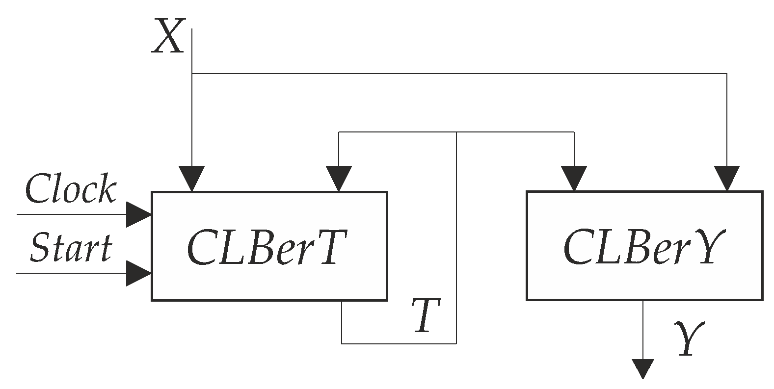
Figure 1).
A block
CLBerT implements SBF (
2). This is accomplished using LUTs and flip-flops. The pulses
Start and
Clock enter
CLBerT to control the flip-flops of
. The functions of SBF (
3) are generated by LUTs of a block
CLBerY.
The modern LUTs have a serious drawback: the number of basic LUT inputs (
) is extremely limited [
13]. This drawback manifests itself in the implementation of LUT-based circuits for functions whose number of arguments exceeds the value
. If a Boolean function
has
arguments, then the corresponding LUT-based circuit requires using super-LUTs if the following condition takes place:
The SBFs (
2) and (
3) are derived from a direct structure table (DST) [
23]. To construct a DST, it is possible to use a state transition graph (STG) [
1]. The STG includes
M nodes corresponding to FSM states. These nodes are connected by arcs corresponding to interstate transitions.
There are H arcs in an STG. If the h-th arc is directed from to , then it determines a transition . The arc number is marked by symbols and . The symbol stands for an input signal determining the transition . The input signal is a conjunction of inputs (or their complements). The symbol denotes a collection of outputs (CO) generated during the transition .
To form a DST, we should transform a graph into an equivalent state transition table. An STT includes columns denoted as (a current state), (a state of transition), (an FSM input), (a collection of outputs), and h (a number of table line).
To construct a DST, it is necessary to encode FSM states
by binary codes
. Compared to an STT, a DST includes the columns with codes
and
as well as a column with a collection of IMFs
. These IMFs determine the next state code [
23].
The most common way to encode states is either using maximum binary or one-hot state assignment. The MBC-based approach provides the minimum width of state codes determined by (
1). But the resulting functions (
2) and (
3) are very complex [
7]. In the case of the OHC-based approach, the codes have the maximum number of bits (
). In this case, it is necessary to use a lot of flip-flops, but the functions (
2) and (
3) are rather very simple. In work [
29], they compared MBC-and OHC-based FSMs. The results of comparison show that a one-hot state assignment provides better results if the number of states exceeds 16. However, in addition to the number of states, the characteristics of LUT-based circuits are also affected by the number of FSM inputs [
30]. The experimental results shown in [
31] prove the following: MBC-based FSMs have better characteristics (as compared with OHC-based FSMs) if the number of FSM inputs exceeds 10.
If the relation (
4) holds for some function
, then this function should be represented as a disjunction of partial functions. This can be accomplished using methods of functional decomposition (FD) [
30]. Each partial function should violate the condition (
4). In this case, such a partial function is generated using a single LUT. Next, these LUTs create a mutual multi-level network. So, FD produces FSM circuits having a lot of logic levels and a very complicated network of “spaghetti-type” interconnections [
32,
33].
The FSM performance may be improved by reducing the amount of LUT levels in an FSM circuit. The reducing the number of literals in the sum-of-products (SOP) of functions (
2) and (
3) can solve this problem. A proper state assignment may optimize SBFs (
2) and (
3) [
32]. An example of such approach efficiency is the algorithm JEDI [
34]. Using JEDI leads to creating generalized cubes covering codes of states for which transitions depend on the same inputs signals
. Using adjacent codes for these states leads to the minimization of SOPs. In turn, this optimizes the corresponding circuits generating SBFs (
2) and (
3): these circuits have fewer LUTs as well as fewer levels and interconnections than the equivalent FSM circuits obtained using both maximum binary and one-hot state codes. As follows from [
35], using JEDI can improve all three basic characteristics of LUT-based FSM circuits.
3. Analysis of CSC-Based Finite State Machines
As the research results [
14] have shown, both temporal and spatial characteristics of MB-FSM circuits can be improved using the composite state codes. As follows from [
14], CSC-based FSM circuits require less chip area and provide better performance compared with MBC-, OHC-and JEDI-based equivalents.
The method proposed in [
14] is based on splitting the set of states
A by
K classes of compatible states
. As a result, a partition
is created. This partition consists of the minimum possible number of elements (classes). The codes
of classes
have
bits:
To create an MBC of classes, the elements of the set
are used.
Inside each class, the states
are encoded by partial state codes
. These codes are maximum binary codes, too. To create the partial codes for a particular class
, it is necessary to have at least
bits, where
To create partial state codes for any class
, we use the variables that form a set
, where
For a state
, the composite state code
is a concatenation of codes
and
:
In (
8), the symbol “∗” is a concatenation sign.
Three sets of variables are determined by each class . The first one is a partial set of inputs having elements. The input signals consisting of variables cause transitions from the states . The partial outputs form the set . This set consists of FSM outputs produced under the influence of inputs . The third set is a partial set of IMFs . The impact of the inputs leads to the generation of outputs and IMFs .
Each class
satisfies the following condition:
In [
36], there is proposed a greedy algorithm creating the partition
with the minimum possible number of classes,
K.
The same variables
represent the bits of partial codes for any class
. So, the total number of used variables (
) is determined as
The partial functions are represented by the following SBFs:
Functions (
11) and (
12) should be transformed into the final values of corresponding functions
. These resulting values are represented as
The functions (
13) and (
14) can be viewed as multiplexing functions [
7] where each conjunction of variables
determines which partial function must be passed to the multiplexer output. Obviously, the dedicated multiplexers of CLBs [
28,
37] could be used for implementing circuits generating functions (
13) and (
14).
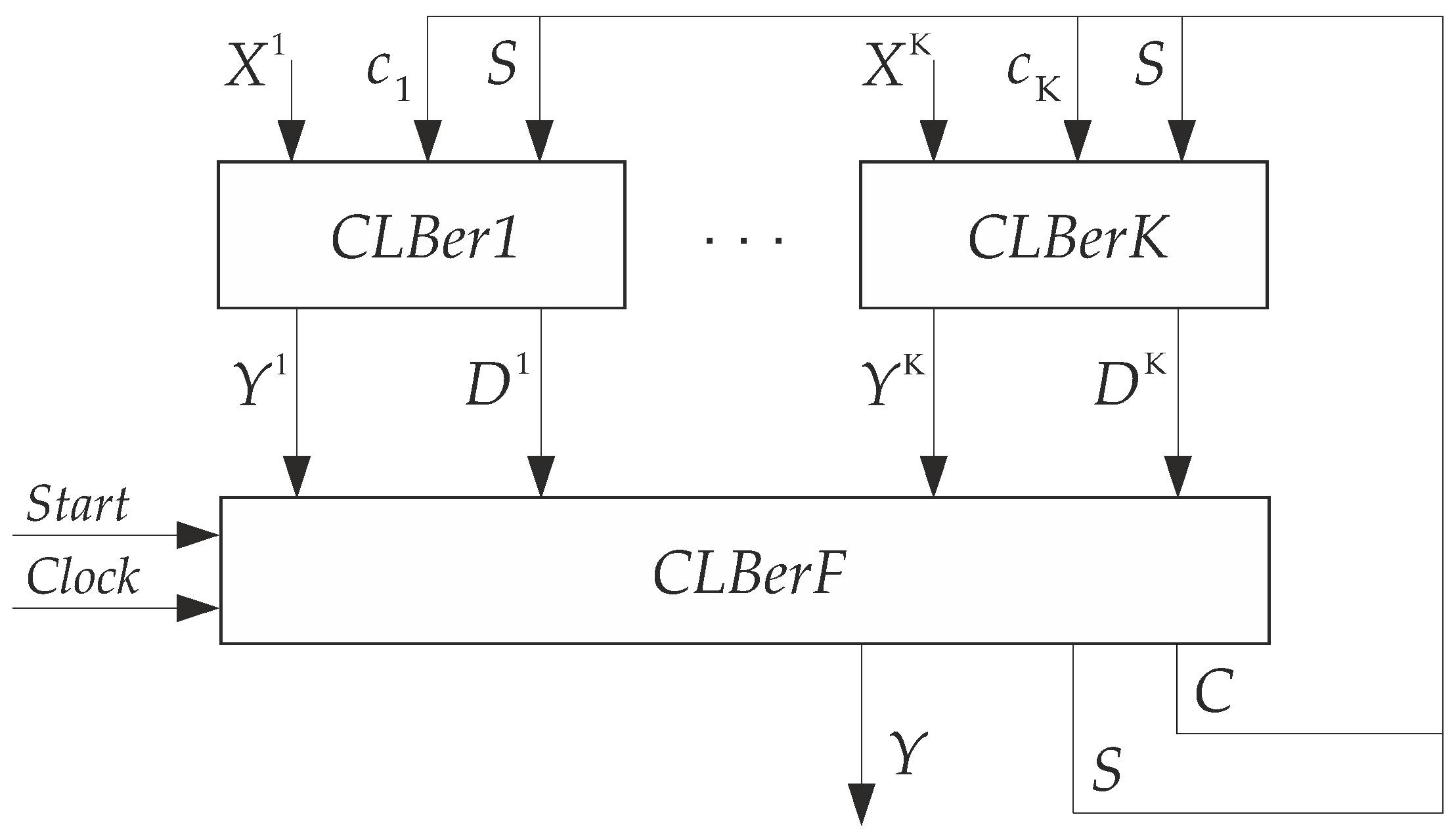
The SBFs (
11)–(
14) determine the architecture of
Mealy FSM. This architecture (
Figure 2) is proposed in the following article [
14].
In
FSM, CLB-based blocks (
CLBer1–
CLBerK) represent the first logic level of the FSM circuit. The
CLBerk generates partial functions having the superscript
k. A
CLBerF generates FSM outputs (
14). Also, this block includes the hidden distributed register
having
flip-flops. Thus, the block
CLBerF implements IMFs (
13) entering inputs of flip-flops. The outputs of flip-flops are the variables
and
. In this way, both class and partial state codes are created.
The article [
14] presents the results of experimental studies aimed at comparing the characteristics of
FSMs with characteristics of equivalent FSMs based on MBCs and OHCs. These results show that CSC-based FSMs have significantly better spatial characteristics than those of the other models studied. It is very important that the improving spatial characteristics do not worsen the temporal characteristics.
As follows from [
14], CSC-based FSMs could be used if the following condition holds:
If the condition
is true, this leads to a single-level circuit of
CLBerF. In this case, there are exactly two levels of LUTs in the circuits of
FSMs. This is the best situation for using the composite state codes.
If condition (
16) is violated, then the circuit of
CLBerF is multi-level. This increases the number of LUTs and their interconnections in comparison with the equivalent single-level circuit. Thus, the violation of condition (
16) leads to the deterioration of the increasing chip area occupied by the FPGA-based circuit of an FSM using CSCs.
Note that the circuit of
CLBerF can be single level even if the condition (
16) is violated. Let us explain this phenomenon. Any function
is represented by
partial functions. If the condition (
16) is violated, then the following condition may take place:
If condition (
17) holds, then there is a single-LUT circuit implementing the corresponding function. If condition (
17) is true for all functions
, then the circuit of the block
CLBerF is single level.
If (
17) is violated, then the circuit of
CLBerF is multi-level. But even in this case, the CSC-based FSMs have better characteristics than their counterparts based on functional decomposition [
14]. If the CSC-based FSM is the control device of a digital system, then decreasing the number of logic levels in the circuit of CLBerF will increase the performance of this digital system. This is also very important for accelerating, for example, the real-time analysis of defect detection in composite materials. Faster FSMs can improve the industrial quality control [
38].
To diminish the number of logic levels in a CRC-based FSM, it makes sense to decrease the number of arguments in SOPs (
13) and (
14). One of the possible ways for solving this problem is the elimination of class variables from these SOPs. In this article, we propose such an approach.
4. The Essence of Proposed Method
In our current paper, we propose a method which eliminates the entry of class variables
into a block
CLBerF. In this case, the classes
are encoded by one-hot codes. The states are still encoded by the maximum binary partial codes. Now, the set
C includes
K elements:
. These variables enter LUTs from the first level of the FSM circuit. The variable
enters all LUTs of the block
CLBerk. The method is focused on the situation when the following condition is violated:
The value
is equal to the maximum number of SLUT inputs that are possible within one block of a CLB. For example, there is
for CLBs of the Virtex-7 family [
27]. If condition (
18) is violated, then there are at least two levels of CLBs in the circuit of
CLBerF. So, there are at least three levels of CLBs in the circuit of
FSM. The proposed method allows obtaining a circuit having exactly two levels of CLBs. Therefore, if condition (
18) is violated, there should be a performance gain in the transition to the proposed class coding method.
Because variables
enter the first logic level, the SBFs (
11) and (
12) should be changed. Now, the following SBFs are generated by blocks
CLBer1-
CLBerK:
In this case, there are no connections between variables
and
CLBerF. This means that SBFs (
13) and (
14) are transformed in the following way:
As before, IMFs (
20) are transformed into class variables
and state variables
. The transition from SBFs (
11)–(
14) to SBFs (
19)–(
22) transforms the initial
FSM into
FSM. The letters “OH” in the subscript “COH” mean that the classes
are encoded by OHCs. The proposed architecture of
FSM is shown in
Figure 3.
In
FSM, SBFs (
19) and (
20) are generated by LUTs from the first logic level. These LUTs create the blocks
CLBerk (
). The LUTs of block
CLBerF generate the final values of FSM outputs
, class variables
and state variables
. Pulses
Start and
Clock enter control inputs of flip-flops creating the hidden register
. This register consists of
flip-flops:
As follows from comparison of the formulae (
10) and (
23), the
of
FSM has more flip-flops than the
of equivalent
FSM. The difference is equal to (
).
To create the partition
, we use the greedy algorithm proposed in [
39]. The condition (
9) still determines the compatibility of states. So, equivalent
and
FSMs have the same number of blocks
CLBerk. But LUTs of
FSM require the additional input for the variable
. Obviously, it can lead to the necessity of using more than a single basic LUT for implementing a circuit for some partial Boolean function.
For each class of the partition
, each partial function
is represented by an SOP having
literals. If the condition
holds, then including the variable
in this SOP still leads to a single-LUT circuit implementing this partial function. If (
24) is violated, then the function
is represented by a multi-LUT circuit. Until the condition
holds, then there are enough resources of a single CLB to implement the circuit generating the partial function
. This circuit is still fast, because the performances of super-LUTs and basic LUTs are practically the same [
28].
If (
25) is violated, then it is necessary to combine several CLBs to obtain the circuit for function
. This leads to slow circuits with complicated systems of interconnections [
28]. If the condition (
24) is violated, it makes sense to apply the adjacent codes for some states
by adjacent codes. To accomplish such a state assignment, we can use the algorithm JEDI [
34].
Consider the following situation. A class
belongs to the partition
created for
FSM. This class determines a set
. Using (
6) gives the value
and the set
. Now, we are going to design the equivalent
FSM using basic LUTs having
. We can implement a super-LUT having five inputs using two basic LUTs and a single dedicated multiplexer. Furthermore, we use the symbol
to denote the conjunction of state variables corresponding to the partial code
.
Consider the following SOP created for some partial function
:
Because there is
, the expression (
26) is characterized by the value
. Obviously, the corresponding circuit is implemented by a single basic 4-LUT. Let states
be encoded in the following way:
,
,
, and
. In this case, Equation (
26) is transformed into the following equation:
When switching to the equivalent
FSM, the expression (
27) must be logically multiplied by
determining the class
. This gives the expression
There is
for SOP (
28). So, the corresponding circuit includes two 4-LUTs and a dedicated multiplexer (
Figure 4a).
To optimize the circuit (
Figure 4a), we propose to use JEDI-based approach. In this case, partial codes of states
,
should be adjacent. One of the possible outcomes is the following:
,
,
, and
. Now, partial codes of states
,
are covered by the generalized cube 0x. Using these codes turns (
28) into the following expression:
Now, there is
for the SOP of
. As a result, there is a single 4-LUT in the corresponding circuit (
Figure 4b). Obviously, inside each class
, states should be encoded using the JEDI-based style of assignment.
Let us discuss the proposed method for designing LUT-based Mealy FSMs. We assume that an FSM is represented by its STG. This method is the following:
Transforming the initial STG into a state transition table.
Creating the partition of set A with the minimum number of classes, K.
Encoding of classes by one-hot codes .
Encoding of states by partial maximum binary codes .
Creating composite state codes .
Creating tables of blocks CLBer1–CLBerK.
Deriving SBFs (
19) and (
20) representing the first logic level of the FSM circuit.
Creating table of block CLBerF.
Deriving SBFs (
21) and (
22) representing the second logic level of the FSM circuit.
Implementing the LUT-based circuit of FSM.
Obviously, if an FSM is represented by its STT, then there is no need in the execution of step 1. The partition
may be obtained using the approach from the article [
39]. This greedy approach minimizes the value of
K. Now, we will discuss an example of synthesis through applying the proposed method.
5. Example of Synthesis of Mealy FSM
Consider an STG (
Figure 5) representing a Mealy FSM
. In this section, there is a synthesis example for the
Mealy FSM
. The FSM circuit is implemented using basic LUTs having
.
Step 1. The three following sets could be derived from
Figure 5:
,
, and
. These sets are characterized by the following cardinality numbers:
,
and
, respectively. The STGs have 24 arcs. So, the corresponding STT has
rows (
Table 1).
Each row of an STT corresponds to some STG arc. The following notation is used in
Table 1:
is a current state corresponding to the vertex from which the
h-th arc leaves;
is a next state corresponding to the vertex in which the
h-th arc enters;
is an input signal (a conjunction of variables
) written above the
h-th arc;
is a collection of FSM outputs written above the
h-th arc (
); h is a number of transitions (
). The transition for an STG to an equivalent STT is transparent and straightforward [
1].
Step 2. This step is executed using the greedy algorithm proposed in [
39]. There is
. This transforms condition (
9) in the following way:
. Applying the method from [
39] gives the partition
with
.
The states
are distributed in the following way:
,
, and
. These classes correspond to the following sets of inputs and outputs:
,
,
,
,
and
. For each class, using (
6) gives
. Using (
7) gives
. There is
for each class
. So, to generate any partial function, it is enough of a single LUT having five inputs.
Step 3. There is . This gives the value and the set . There is no influence of class codes on the FPGA area required for implementing the circuits of CLBer1–CLBerK. Due to it, we can encode the classes in the following way: , , and .
Step 4. As we found earlier, the set of partial state variables contains elements: . The same variables are used to encode states for any class .
To select partial state codes, it is necessary to split the source STT into K subtables, each of which corresponds to a certain class . Next, we should use the algorithm JEDI for optimal state encoding. Naturally, this makes it possible to optimize only partial SOPs for functions .
Using this approach, we can assign the following partial codes. For the class , there are the following codes: , , , and . For the class , there are the following codes: , , , and . For the class , there are the following codes: , , and .
Obviously, there are elements in the set of IMFs. In the discussed case, there is a set . The IMFs determine the class codes. The other three IMFs determine the partial state codes.
Step 5. Using (
10) gives
. As follows from (
8), to create composite state codes, we should use both class and partial state codes. For the discussed example, these codes are the following:
,
,
,
,
,
,
,
,
,
, and
.
In these codes, the class code is represented by the first three digits, and the partial state code is represented by two digits. These codes are used in tables of CLBer1-CLBer3.
Step 6. In the discussed case,
CLBer1 is represented by
Table 2,
CLBer2 by
Table 3, and
CLBer3 by
Table 4. These tables have the following columns:
,
,
,
,
,
,
, and
h. For each state, the columns
,
,
, and
are the same as they are in
Table 1. The column
is filled using the code
.
Step 7. Table 2,
Table 3 and
Table 4 are used for deriving SBFs (
10)–(
20). This is accomplished in two stages. Stage 1 is reduced to creating partial SOPs using partial state codes and FSM inputs. During stage 2, the final values of SOPs are created by multiplying the outcomes of stage 2 by the corresponding class variable.
For our example, we show only SOPs of partial functions
(they are derived from
Table 2),
(they are derived from
Table 3) and
(they are derived from
Table 4). These partial SOPs are represented by the following equations:
In these systems, variables
represent product terms corresponding to the
CLBerk lines of the table. We combine some groups of terms and place them into square brackets to show that these terms can be represented by a single conjunction [
1]. We hope there is a transparent connection between SBFs (
30) and (
31) and
Table 2,
Table 3 and
Table 4, respectively.
Step 8. The table of
CLBerF shows which partial functions should be connected using logical disjunction. Using this information, the final values of FSM outputs and IMFs are created. There are the following columns in this table: “F”,
. The row number
j corresponds to a function
. These functions are written in the column “F”. The column number
k corresponds to the partial function
. This column contains information about the participation of a particular partial function in the formation of the final value of function
. If a function
is generated by an LUT of
CLBerk, then there is a sign “+” on the intersection of the column
k and row
j. In the discussed case,
CLBerF is represented by
Table 5.
Step 9. Using
Table 5 allows obtaining a system of disjunctions representing functions
. In the discussed case, the functions
and
are represented by SBF (
32):
Using a similar approach, we can obtain the SOPs of all functions belonging to SBFs (
19) and (
20). The IMFs enter inputs of flip-flops. This results in generating the class variables
and state variables
on the outputs of
CLBerF.
Step 10. To implement the FPGA-based circuit, it is necessary to apply some industrial CAD tools. These tools execute the technology mapping [
30,
40]. In the case of Virtex-based design, we should use the package Vivado [
41]. We do not discuss this step for our example.
Now, we are going to evaluate the temporal and spatial characteristics of the designed LUT-based FSM circuit. For a rough estimate of the cycle time, we should find the number of CLB levels in the circuit. The spatial characteristic is represented by an LUT count. To design the circuit, we use five-input LUTs.
As follows from
Table 2, the LUTs of
CLBer1 generate six output functions and five input memory functions. We analyzed the minimized SBFs (
19) and (
20) for this block. The minimization is executed by an algorithm, JEDI. As a result of the analysis of the output functions
, we found that seven LUTs and one dedicated multiplexer are enough to generate them. To implement a circuit generating the partial function
, two 5-LUTs are combined into a super-LUT. To accomplish this, we use a dedicated multiplexer. As a result of the analysis of the IMFs
, we found that eight LUTs and three dedicated multiplexers are enough to generate them. The circuit of
CLBer1 includes 15 basic LUTs and four dedicated multiplexers. Also, this circuit has a single level of CLBs. To implement circuits for some functions
, it is necessary to combine two LUTs. But this is accomplished using internal fast interconnections of a CLB [
28]. So, this combining practically does not affect the time characteristics (compared with single-LUT circuits).
A similar analysis was performed for the blocks CLBer2 and CLBer3. As a result, it was found that: (1) the circuit of block CLBer2 includes 14 LUTs and four multiplexers, and (2) the circuit of block CLBer3 includes 13 LUTs and one multiplexer. Both schemes include one level of CLBs. But some functions are generated by SLUTs.
So, there are 42 LUTs and nine multiplexers on the first logic level of the designed FSM circuit. The circuit has one level of CLBs, although some functions are generated using super-LUTs.
As follows from
Table 5, there are 12 basic LUTs in the circuit of
CLBerF. The output
is generated only by an LUT of
CLBer1. Due to it, there is no need to use an LUT of
CLBerF to generate the output
. To generate any other function, it is enough to use either two or three inputs of basic 5-LUTs. So, the circuit of
CLBerF is a single-level. Moreover, there is no need in using dedicated multiplexers (each function is represented by a single-LUT circuit).
To summarize, the designed FSM circuit consists of 52 basic LUTs and nine dedicated multiplexers. There are two levels of CLBs in this circuit. Each partial function is implemented by a circuit having almost the same latency time as a single-LUT circuit (this effect is achieved through the use of intra-CLB dedicated multiplexers).
To analyze the efficiency of the proposed approach and some other known methods, we have conducted a lot of experiments. We have compared the characteristics of
FSMs with characteristics of their counterparts based on MBCs, OHCs and CSCs. The results of the experiments are shown in
Section 6.
6. Experimental Results
We have conducted the experiments to compare the temporal (maximum operating frequencies) and spatial (LUT counts) characteristics of FSM circuits based on various known state encoding methods and circuits of
FSMs. As an example of the MBC-based method, we use the method Auto of Vivado [
41]. The one-hot of Vivado [
41] is used as an example of an OHC-based state assignment. Also, we compared our approach with the algorithm JEDI [
34], which is an MBC-based algorithm creating cubes covering codes of some states [
30]. We compared the proposed approach with
FSMs [
14].
In experiments, we use benchmark FSMs from the well-known library LGSynth93 [
42]. There are 48 Mealy FSMs (benchmarks) in the library. The benchmarks are represented in the format KISS2. The benchmark FSMs have a wide range of basic characteristics (numbers of states, inputs, outputs, and transitions). A lot of scientists have been using these benchmarks as a basis for the comparison of various design methods [
43,
44,
45]. The characteristics of benchmarks are shown in
Table 6. The last column of this table includes the summarized number of FSM inputs and bitness of MBCs (
). We explain a bit later why this column is added.
To conduct the experiments, we use a platform including the FPGA chip of the Virtex-7 family. This is a VC709 Evaluation Platform (xc7vx690tffg1761-2) [
27]. The CLBs used include basic LUTs with six address inputs (
). To implement a CLB-based circuit of
CLBerF, the dedicated multiplexers can be used. Each CLB includes four basic LUTs and three dedicated multiplexers. We use the industrial CAD package Vivado v2019.1 (64-bit) [
41] to execute the step of technology mapping. Using the Vivado reports, we created four tables showing the results of the conducted experiments.
Each Boolean function
depends on
arguments. If condition (
4) is violated for all IMFs and FSM outputs, then there are exactly
LUTs in the circuit of MB-FSM. Also, such a circuit is single level. Obviously, if condition (
4) is violated, then the LUT-based MB-FSM circuit has the best possible characteristics: the minimum values of LUT count and time of cycle. In this case, there is no need for the optimization of such a circuit. So, in this case, it makes sense just to use the model of MB-FSM.
As shown in [
14], the condition (
4) holds if a benchmark included into the library [
42] satisfies the following relation:
If condition (
33) holds, then we can replace MBC-based FSMs with FSMs with composite state codes. Thus, it makes sense to use either CSC- or MSC-based models for those FSMs, where relation (
33) holds. There is
. So, we show experimental results only for the benchmarks satisfying the condition
. The experimental results are shown in
Table 7 (cycle times, nanoseconds),
Table 8 (maximum operating frequency, MHz),
Table 9 (LUT counts),
Table 10 (area-time products), and
Table 11 (power consumption).
There are the following columns in
Table 7,
Table 8,
Table 9,
Table 10 and
Table 11: FSM (names of benchmark FSMs); MB (experimental results for FSMs with maximum binary state codes); OH (experimental results for FSMs with one-hot state codes); JEDI (experimental results for FSMs whose state codes are encoded using the JEDI algorithm);
(experimental results for FSMs with composite state codes);
(our new approach);
. The results of the summation of values from the corresponding columns are shown in the row “Total”. The row “Percentage” shows the percentage of summarized characteristics of investigated FSM circuits, respectively, to
FSMs.
The main goal of the proposed method is the increasing performance of LUT-based FSM circuits in relation to the circuits of
-based FSMs. Due to this, we start the research analysis from cycle times (
Table 7).
Table 7.
Results of experiments (cycle time, nsec).
Table 7.
Results of experiments (cycle time, nsec).
| FSM | MB | OH | JEDI | | | |
|---|
| ex1 | 6.625 | 7.155 | 5.654 | 3.620 | 3.456 | 16 |
| kirkman | 7.073 | 6.494 | 6.382 | 4.359 | 3.956 | 18 |
| planet | 7.535 | 7.535 | 5.344 | 3.491 | 3.342 | 14 |
| planet1 | 7.535 | 7.535 | 5.344 | 3.491 | 3.342 | 14 |
| pma | 6.841 | 6.841 | 5.888 | 4.080 | 3.762 | 14 |
| s1 | 6.830 | 7.361 | 6.363 | 4.233 | 3.948 | 14 |
| s1488 | 7.220 | 7.579 | 6.362 | 4.384 | 4.181 | 15 |
| s1494 | 6.694 | 6.861 | 6.085 | 4.420 | 4.141 | 15 |
| s1a | 6.520 | 5.669 | 5.911 | 4.521 | 4.196 | 15 |
| s510 | 5.629 | 5.629 | 5.512 | 4.581 | 3.627 | 27 |
| s820 | 6.579 | 6.529 | 5.663 | 4.419 | 3.605 | 25 |
| s832 | 6.863 | 6.526 | 5.754 | 4.553 | 3.871 | 25 |
| sand | 8.623 | 8.623 | 7.885 | 4.424 | 4.094 | 18 |
| styr | 7.267 | 7.697 | 6.866 | 3.719 | 3.537 | 16 |
| tma | 6.102 | 6.766 | 6.092 | 3.557 | 3.608 | 13 |
| Total | 103.937 | 104.800 | 91.106 | 61.851 | 56.666 | |
| Percentage, % | 183.42 | 184.94 | 160.78 | 109.15 | 100.00 | |
As follows from
Table 7, the proposed method of creating composite state codes makes it possible to obtain LUT-based FSM circuits with shorter cycle times than those of the other studied FSMs. As can be seen from
Table 7,
-based FSMs have the following gain: (1) 83.42% compared with MBC-based FSMs; (2) 84.94% compared with OHC-based FSMs; (3) 60.78% compared with JEDI-based FSMs and (4) 9.15% compared with
-based FSMs.
Now, we are going to compare the temporal characteristics of equivalent
and
FSMs. Consider the results for the benchmark
tma. As follows from
Table 7, our method produces a bit slower circuit than the circuits produced using the approach [
14]. The loss is around 1.5%. However, our method gives a payoff starting from the FSMs for which
(
planet,
planet1,
pma,
s1). There is the gain equal to 26.3% for the most complex benchmark
s510 having the number 27 in the last column. There is the gain in 22.5% for
s820 and 17.7% for
s832. Both benchmarks have
. So, the gain from the applying the proposed method increases with the growth of the value
.
We think that this phenomenon is related to the difference in the number of CLBs connected in series in the CLBerF circuit. As the value of increases, the number of consecutive CLBs grows faster for FSMs than for equivalent FSMs. From this, we can conclude that the proposed method leads to LUT-based FSM circuits with better temporal characteristics compared with these characteristics of equivalent FSM circuits.
The values of cycle times are taken directly from the Vivado reports. Using the values from
Table 7, we can obtain the values of the maximum operating frequencies. These results are shown in
Table 8.
Table 8.
Results of experiments (maximum operating frequency, MHz).
Table 8.
Results of experiments (maximum operating frequency, MHz).
| FSM | MB | OH | JEDI | | | |
|---|
| ex1 | 150.94 | 139.76 | 176.87 | 276.23 | 289.31 | 16 |
| kirkman | 141.38 | 154.00 | 156.68 | 229.41 | 252.77 | 18 |
| planet | 132.71 | 132.71 | 187.14 | 286.48 | 299.26 | 14 |
| planet1 | 132.71 | 132.71 | 187.14 | 286.48 | 299.26 | 14 |
| pma | 146.18 | 146.18 | 169.83 | 245.12 | 265.83 | 14 |
| s1 | 146.41 | 135.85 | 157.16 | 236.24 | 253.29 | 14 |
| s1488 | 138.50 | 131.94 | 157.18 | 228.12 | 239.18 | 15 |
| s1494 | 149.39 | 145.75 | 164.34 | 226.23 | 241.48 | 15 |
| s1a | 153.37 | 176.40 | 169.17 | 221.18 | 238.32 | 15 |
| s510 | 177.65 | 177.65 | 181.42 | 218.31 | 275.72 | 27 |
| s820 | 152.00 | 153.16 | 176.58 | 226.28 | 277.41 | 25 |
| s832 | 145.71 | 153.23 | 173.78 | 219.65 | 258.32 | 25 |
| sand | 115.97 | 115.97 | 126.82 | 226.03 | 244.24 | 18 |
| styr | 137.61 | 129.92 | 145.64 | 268.92 | 282.74 | 16 |
| tma | 163.88 | 147.80 | 164.14 | 281.14 | 277.16 | 13 |
| Total | 2184.41 | 2173.03 | 2493.89 | 3675.82 | 3994.29 | |
| Percentage, % | 54.69 | 54.40 | 62.44 | 92.03 | 100.00 | |
As follows from
Table 8, the proposed method produces FPGA-based FSM circuits with higher frequencies than the other studied FSMs. As can be seen from
Table 8,
-based FSMs have the following gain: (1) 45.31% compared with MBC-based FSMs; (2) 45.60% compared with OHC-based FSMs; (3) 37.56% compared with JEDI-based FSMs and (4) 7.87% compared with
-based FSMs. The reasons for this state of affairs have already been considered in the analysis of the data from
Table 7. We do not repeat them.
The main goal of the proposed approach is to improve the temporal characteristics of LUT-based FSM circuits in relation to circuits of equivalent
-based FSMs. However, it is very important that the increase in performance did not lead to a significant increase in the number of LUTs used. Comparison of the spatial characteristics of different FSM models is shown in
Table 9.
Table 9.
Results of experiments (LUT count).
Table 9.
Results of experiments (LUT count).
| FSM | MB | OH | JEDI | | | |
|---|
| ex1 | 70 | 74 | 53 | 40 | 48 | 16 |
| kirkman | 42 | 58 | 39 | 31 | 42 | 18 |
| planet | 131 | 131 | 88 | 77 | 82 | 14 |
| planet1 | 131 | 131 | 88 | 77 | 82 | 14 |
| pma | 94 | 94 | 86 | 72 | 78 | 14 |
| s1 | 65 | 99 | 61 | 55 | 61 | 14 |
| s1488 | 124 | 131 | 108 | 87 | 93 | 15 |
| s1494 | 126 | 132 | 110 | 85 | 91 | 15 |
| s1a | 49 | 81 | 43 | 43 | 52 | 15 |
| s510 | 48 | 48 | 32 | 26 | 34 | 27 |
| s820 | 88 | 82 | 68 | 48 | 51 | 25 |
| s832 | 80 | 79 | 62 | 50 | 54 | 25 |
| sand | 132 | 132 | 114 | 91 | 102 | 18 |
| styr | 93 | 120 | 81 | 71 | 81 | 16 |
| tma | 45 | 39 | 39 | 31 | 37 | 13 |
| Total | 1318 | 1431 | 1072 | 884 | 988 | |
| Percentage, % | 133.40 | 144.84 | 108.50 | 89.47 | 100.00 | |
As follows from
Table 7 and
Table 9, an increase in performance by an average of 9% leads to an increase in the LUT counts by an average of 10%.We consider this ratio to be quite acceptable. Note that the proposed approach allows improving the spatial characteristics in comparison with all methods except for the method of maximum encoding of classes used in
FSMs. Our method gains the following on average: (1) 33.4% compared with MB-based FSMs; (2) 44.84% compared with OHC-based FSMs and (3) 8.5% compared with JEDI-based FSMs.
At the same time, for the most complex benchmark FSM s510, the loss reaches around 25%. However, for simpler benchmarks (planet, planet1), the loss is about 6.5%. Thus, an increase in the value of the sum leads to an increase in the loss of the proposed approach in relation to equivalent FSMs.
There are several integral evaluations of the quality of a digital circuit. One of the main integral characteristics is the product of the area of the circuit and its performance (area-time product) [
15]. In the case of LUT-based circuits, the area is estimated using such a characteristic as LUT count. Naturally, performance is measured in terms of cycle time. The smaller the value of this integral characteristic is, the higher the quality of the circuit. Using Vivado reports, we created
Table 10 including values of area-time products for circuits of benchmark FSMs.
Table 10.
Results of experiments (area-time products).
Table 10.
Results of experiments (area-time products).
| FSM | MB | OH | JEDI | | | |
|---|
| ex1 | 463.76 | 529.48 | 299.66 | 144.81 | 165.91 | 16 |
| kirkman | 297.07 | 376.62 | 248.91 | 135.13 | 166.16 | 18 |
| planet | 987.11 | 987.11 | 470.24 | 268.78 | 274.01 | 14 |
| planet1 | 987.11 | 987.11 | 470.24 | 268.78 | 274.01 | 14 |
| pma | 643.04 | 643.04 | 506.39 | 293.73 | 293.42 | 14 |
| s1 | 443.96 | 728.74 | 388.14 | 232.81 | 240.83 | 14 |
| s1488 | 895.31 | 992.88 | 687.11 | 381.38 | 388.83 | 15 |
| s1494 | 843.43 | 905.66 | 669.34 | 375.72 | 376.84 | 15 |
| s1a | 319.49 | 459.18 | 254.18 | 194.41 | 218.19 | 15 |
| s510 | 270.19 | 270.19 | 176.39 | 119.10 | 123.31 | 27 |
| s820 | 578.95 | 535.39 | 385.09 | 212.13 | 183.84 | 25 |
| s832 | 549.04 | 515.56 | 356.77 | 227.63 | 209.04 | 25 |
| sand | 1138.23 | 1138.23 | 898.91 | 402.60 | 417.62 | 18 |
| styr | 675.82 | 923.65 | 556.17 | 264.02 | 286.48 | 16 |
| tma | 274.59 | 263.87 | 237.60 | 110.27 | 133.50 | 13 |
| Total | 9367 | 10257 | 6605 | 3631 | 3752 | |
| Percentage, % | 249.66 | 273.37 | 176.04 | 96.78 | 100.00 | |
As follows from
Table 10, the proposed method makes it possible to obtain LUT-based FSM circuits with slightly larger area-time products than those of their
-based counterparts. The
FSM circuits lose in relation to equivalent CSC-based FSMs (the loss is 3.72%). Obviously, this loss is very small. However, our method provides significantly better results than the other methods studied. The gain is 149.66% in relation to MB-based FSMs, 173.37% in relation to OH-based FSMs, and 76.04% in relation to JEDI-based FSMs.
It is interesting to note that our method always loses if there is . At the same time, there is a gain when there is (benchmarks s820 and s832) but a loss when there is (benchmark s510). It follows from this that the gain or loss depends on how many levels of CLBs are needed to generate partial functions. And this, in turn, depends on the number of arguments in the respective SOPs.
One of the very important issues is the power consumption [
46]. This factor significantly affects the lifetime of mobile and autonomous devices [
46,
47]. As can be seen from
Table 9, our method leads to an increase in the value of LUT count compared to equivalent CSC-based FSMs. This can lead to an increase in power consumption. To check the overhead, we used reports of Vivado. The results are shown in
Table 11.
As follows from
Table 11, the proposed method makes it possible to obtain LUT-based FSM circuits consuming more power than the equivalent
-based FSMs. The
FSM circuits lose in relation to equivalent CSC-based FSMs (the loss is 7.63%). This overhead is connected with the growth of LUT counts and the number of interconnections. However, our method provides significantly better results than the other methods based on both maximum binary codes (the gain is 27.62%) and one-hot state codes (the gain is 29.42%). Also, our method gives a small advantage in relation to JEDI-based FSMs (the gain is 3.03%).
Table 11.
Results of experiments (power consumption, Watts).
Table 11.
Results of experiments (power consumption, Watts).
| FSM | MB | OH | JEDI | | | | |
|---|
| ex1 | 4.564 | 3.430 | 2.804 | 2.612 | 2.351 | 2.539 | 16 |
| kirkman | 2.204 | 2.355 | 1.950 | 1.854 | 1.669 | 1.802 | 18 |
| planet | 4.553 | 4.553 | 2.887 | 2.914 | 2.623 | 2.832 | 14 |
| planet1 | 4.553 | 4.553 | 2.887 | 2.914 | 2.623 | 2.832 | 14 |
| pma | 1.818 | 1.818 | 1.701 | 1.726 | 1.553 | 1.678 | 14 |
| s1 | 3.133 | 3.578 | 2.966 | 3.089 | 2.780 | 3.003 | 14 |
| s1488 | 4.430 | 4.544 | 3.996 | 4.001 | 3.601 | 3.889 | 15 |
| s1494 | 3.527 | 3.626 | 3.430 | 3.523 | 3.171 | 3.424 | 15 |
| s1a | 1.770 | 2.458 | 1.656 | 1.672 | 1.505 | 1.625 | 15 |
| s510 | 2.166 | 2.166 | 1.714 | 1.643 | 1.479 | 1.627 | 27 |
| s820 | 1.128 | 1.197 | 1.124 | 1.142 | 1.028 | 1.131 | 25 |
| s832 | 2.662 | 2.409 | 2.071 | 1.915 | 1.724 | 1.896 | 25 |
| sand | 1.640 | 1.640 | 1.479 | 1.421 | 1.279 | 1.381 | 18 |
| styr | 4.506 | 5.233 | 3.649 | 3.721 | 3.349 | 3.617 | 16 |
| tma | 2.020 | 1.745 | 1.752 | 1.781 | 1.603 | 1.731 | 13 |
| Total | 44.67 | 45.31 | 36.07 | 35.93 | 32.34 | 35.01 | |
| Percentage, % | 127.62 | 129.42 | 103.03 | 102.63 | 92.37 | 100.00 | |
It should be noted that the impact of increased FSM performance can eliminate the shortcomings associated with increased power consumption. As the performance of the control FSM increases, the system performs the necessary calculations faster. Reducing the calculation time leads to less power consumption of the system as a whole. Thus, our method can lead to a decrease in power consumption by the system as a whole despite the increase in consumption by the FSM circuit.
An analysis of the results of the studies carried out allows drawing the following conclusion regarding the equivalent
- and
-based FSMs. If condition (
33) holds, then
FSMs’ circuits have better performance which is not accompanied by a significant deterioration in spatial characteristics (the LUT counts). In this case, the equivalent
- and
-based FSMs have almost the same values of area-time products. This fact means that our approach gains in performance almost as much as it loses in area occupied by FSM circuits. So, the proposed method can be used if the main criterion for the FSM circuit optimality is the maximum performance.


