
Design and Process Implementation of Silicon-Based Carrier for 100 G/200 G Electro-Absorption Modulated Laser Chips

Abstract
1. Introduction
2. Theoretical Framework
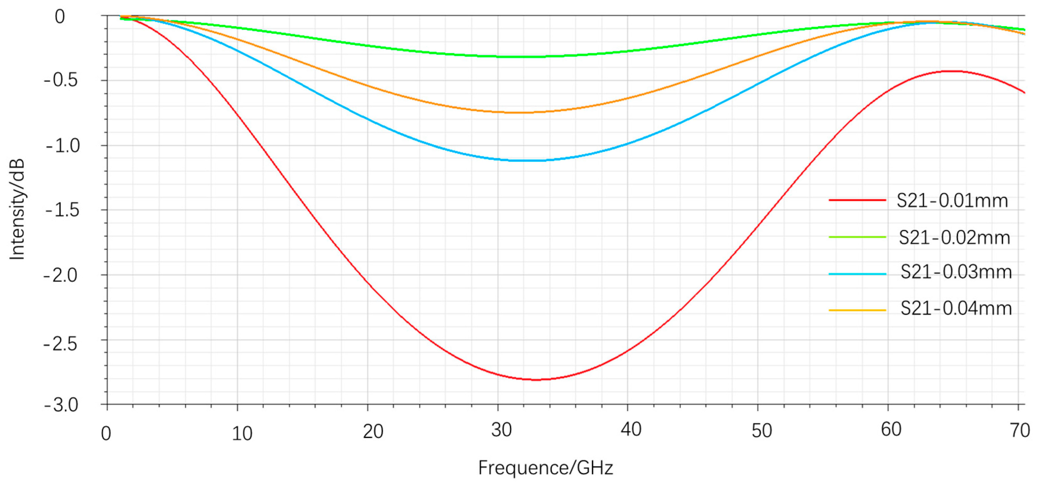
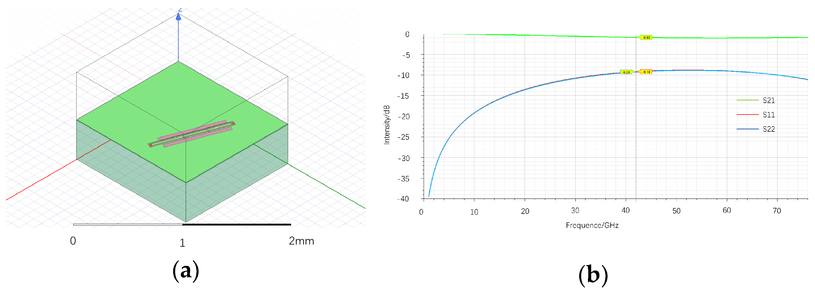
2.1. Low-Loss Coplanar Waveguide (CPW) Transmission
2.2. Multi-Channel Crosstalk Suppression
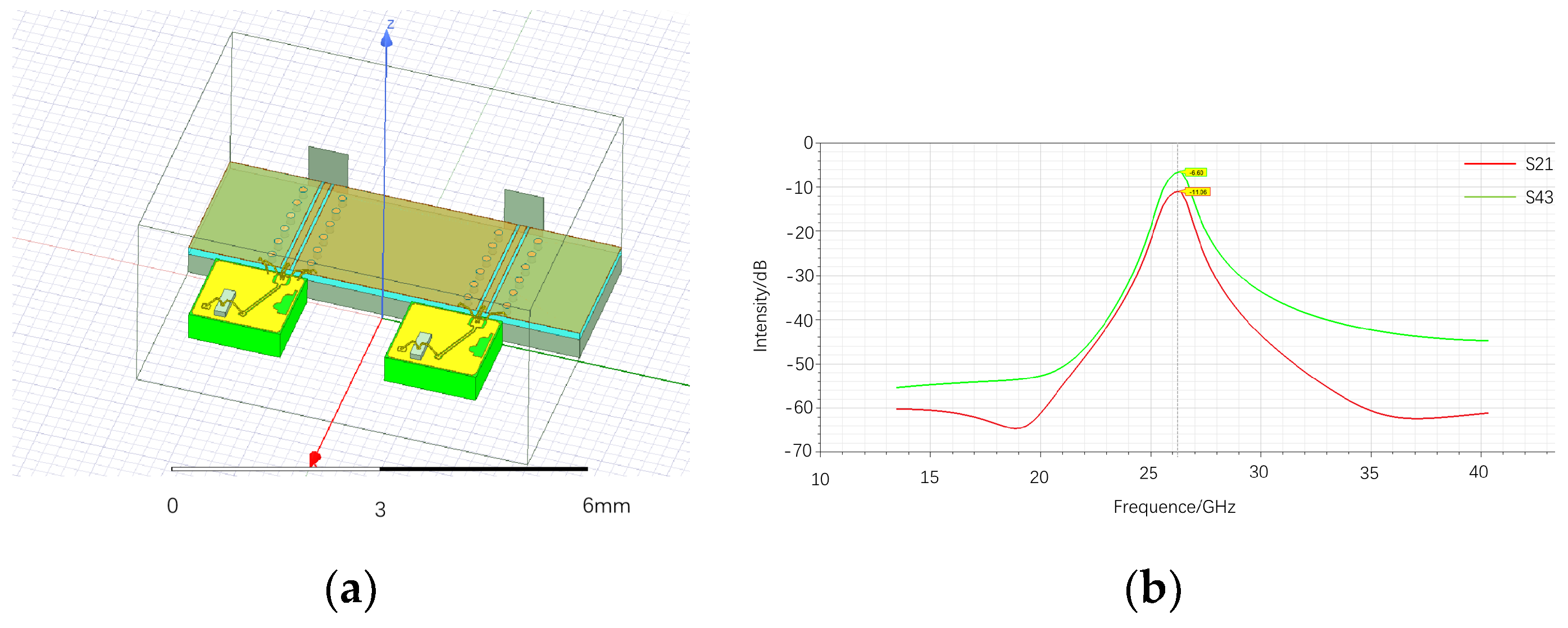
- Dual-Channel Model (Figure 2).
- 2.
- Adding Metal Barriers Between Channels (Figure 3):
- 3.
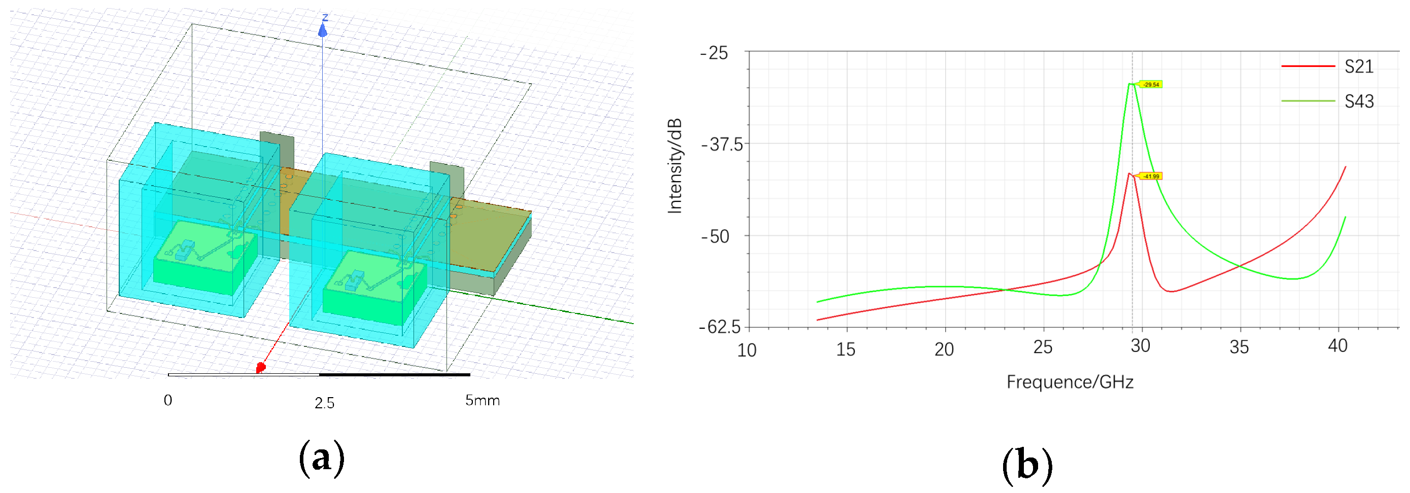
- Adding Absorbing Material Cover (Figure 4):
- 4.
- Adding Bonding Gold Wires (Figure 5):
- 5.
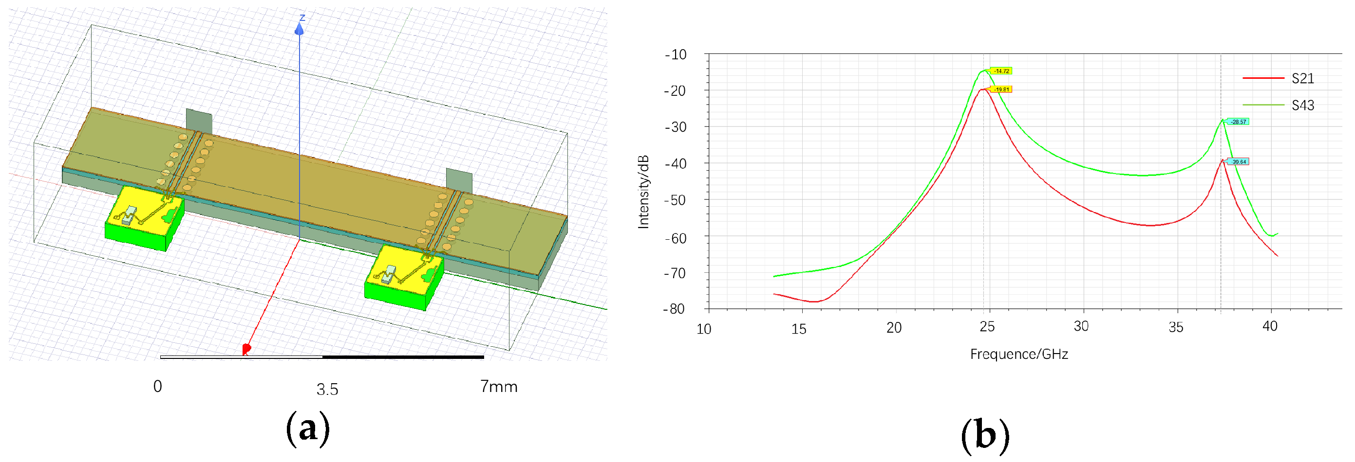
- Increasing Channel Spacing (Figure 6):
2.3. High-Density Capacitor Design
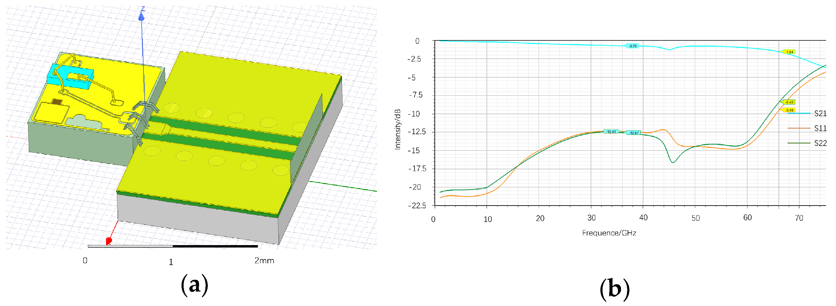
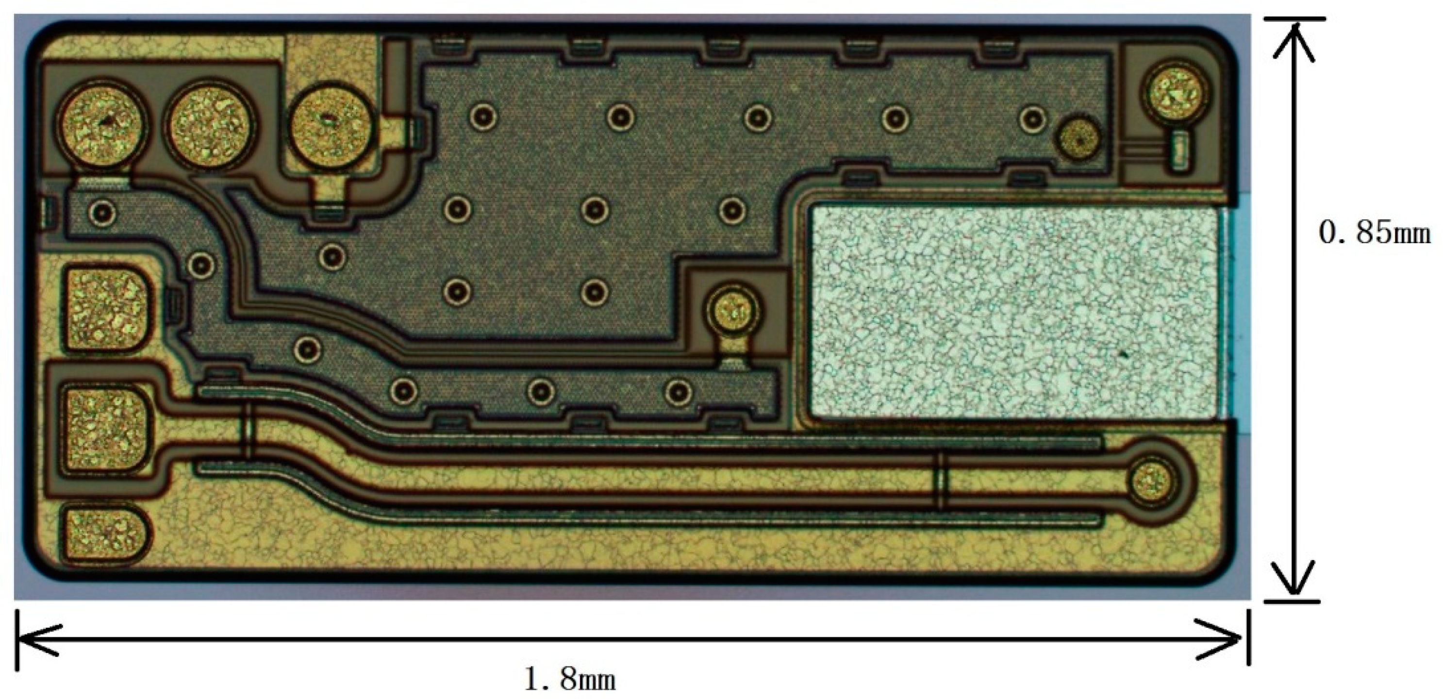
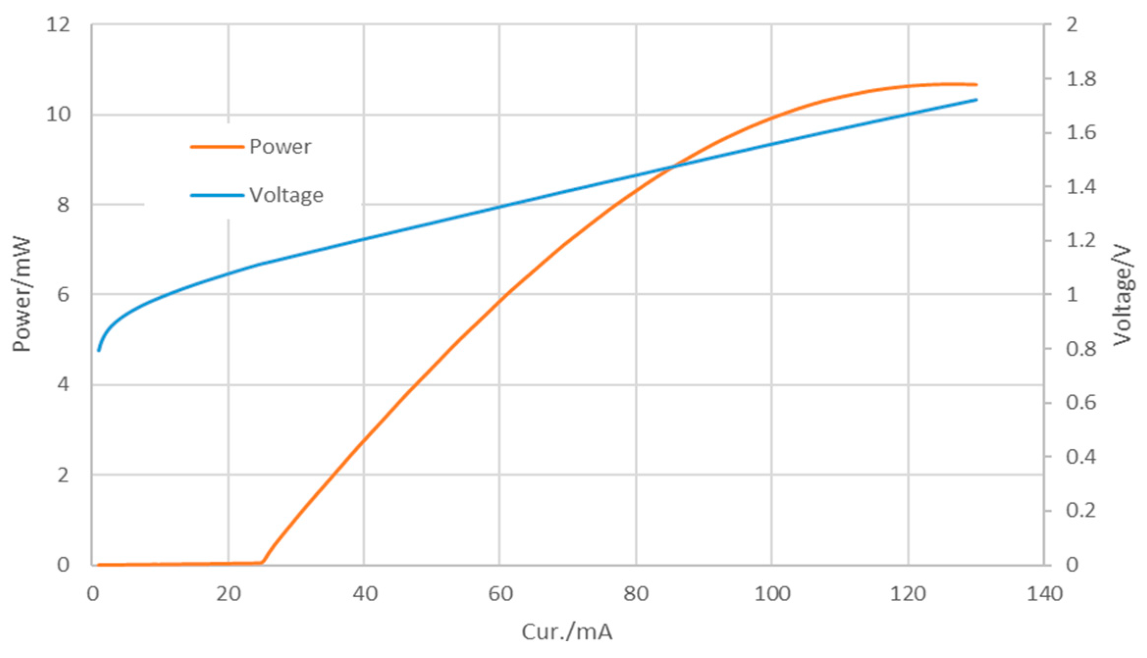
3. Experiments
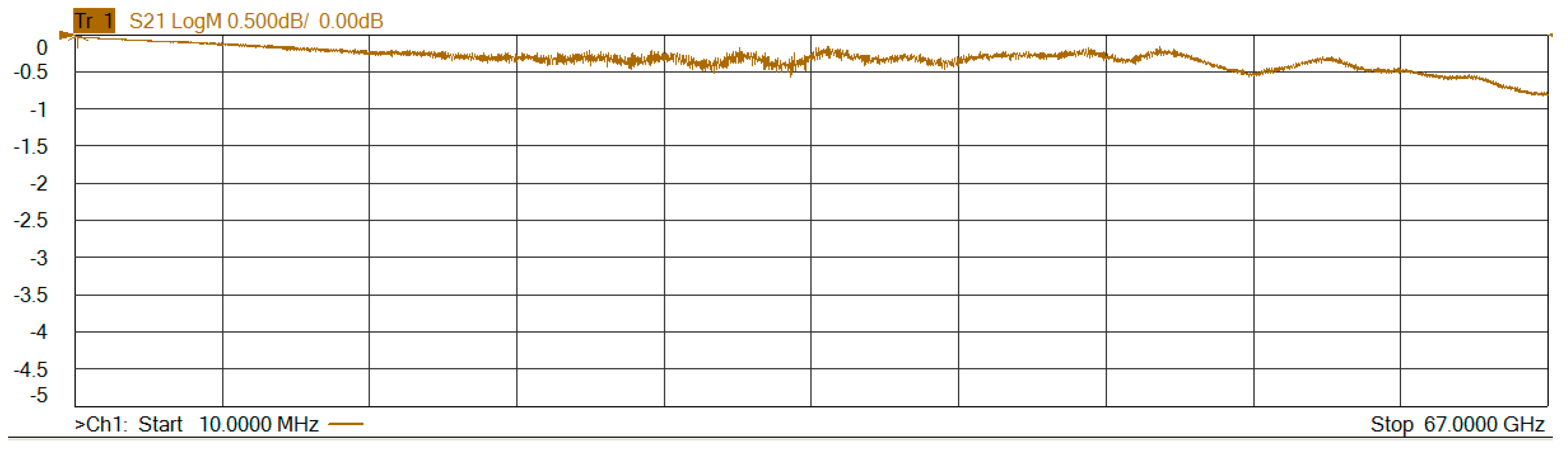
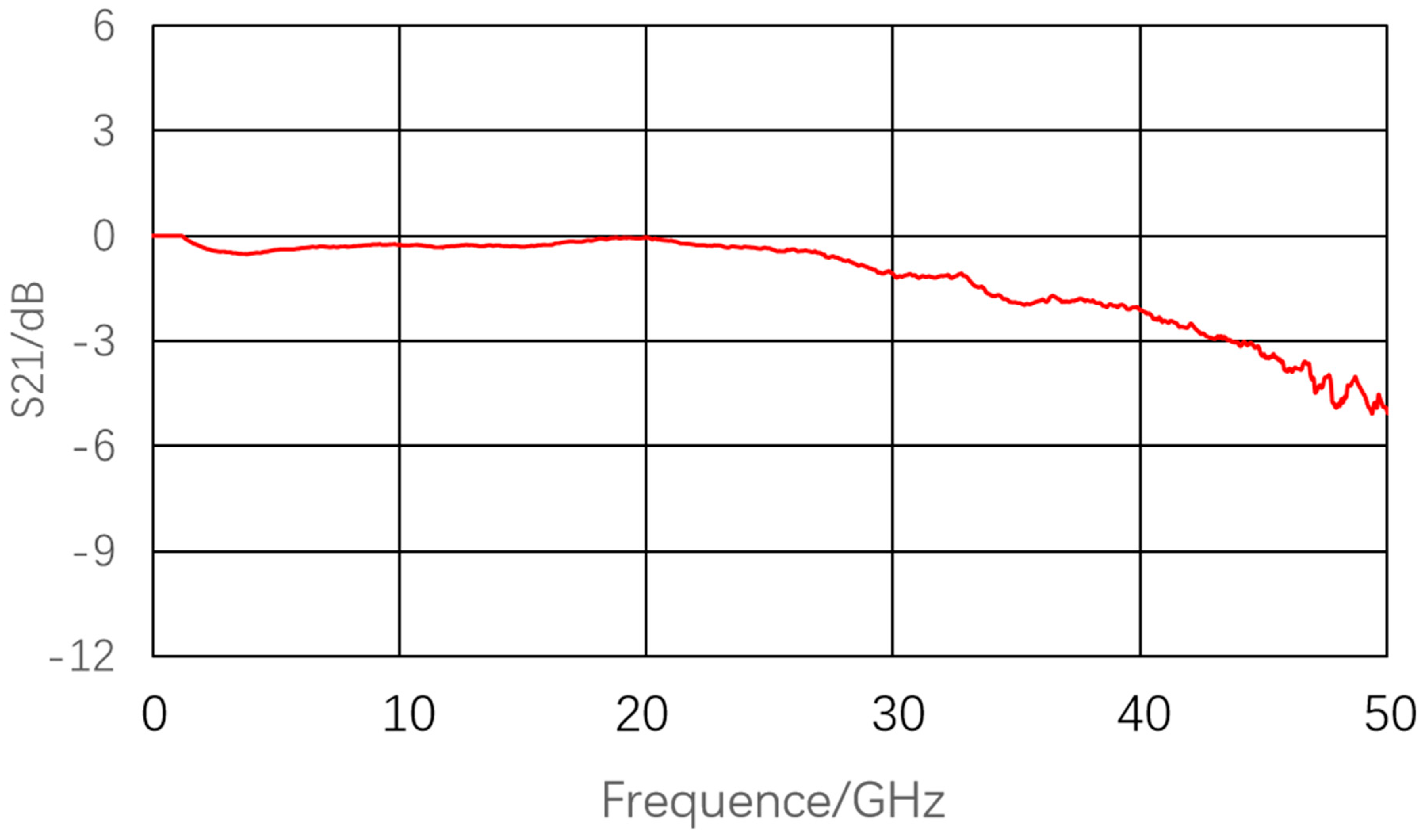
3.1. CPW Transmission Line Optimization
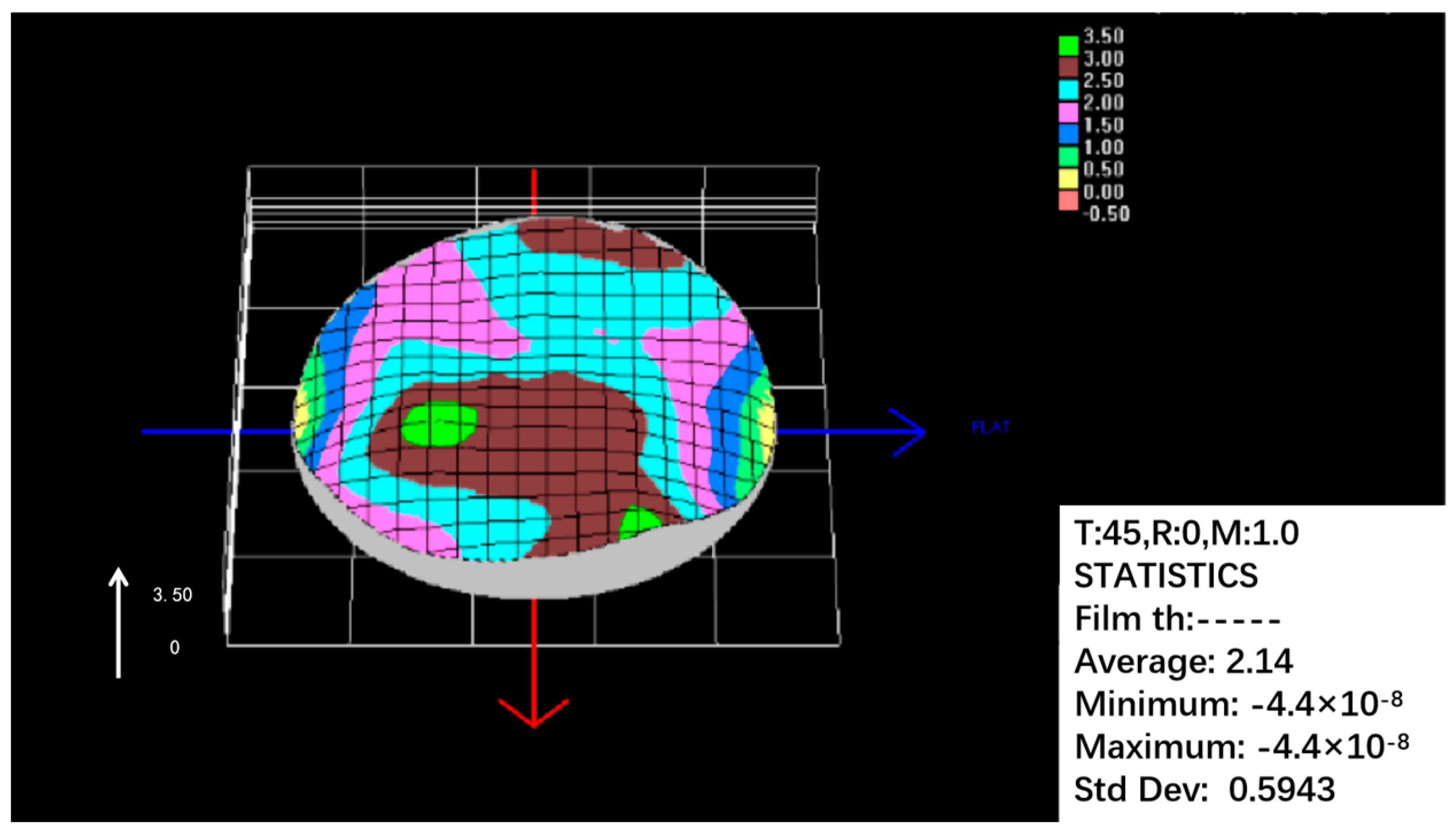
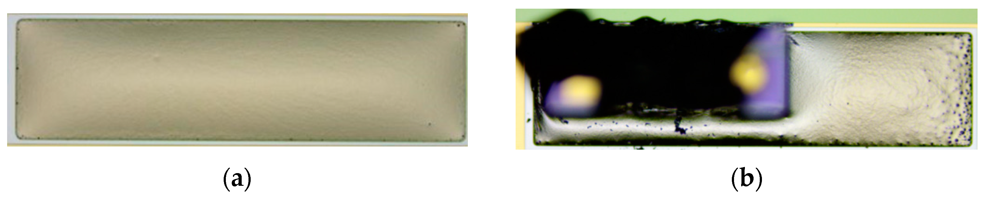
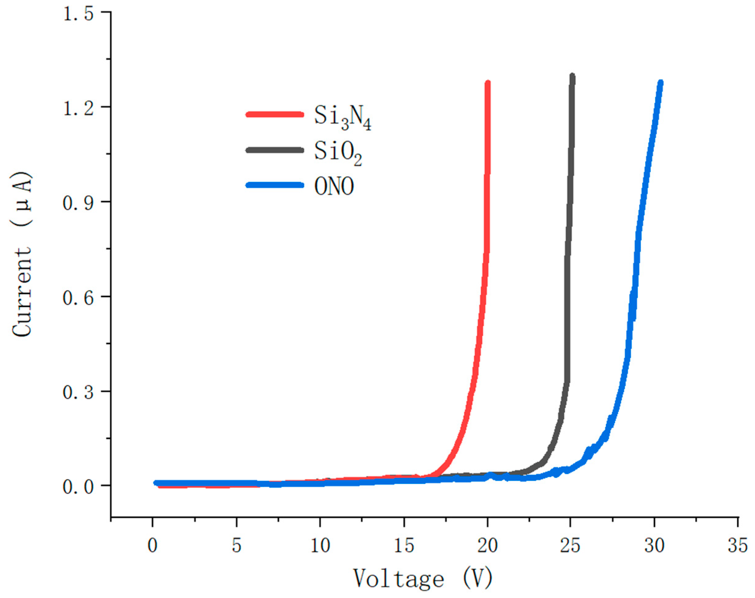
3.2. High-Density Capacitor Process Optimization
- Dielectric Material Optimization
- 2.
- Three-Dimensional Electrode Design
- 3.
- Etching Process Improvement
- 4.
- Polysilicon Filling Optimization
- 5.
- High-Speed Silicon Carrier Performance Testing
- Transmission line width: 0.01 mm~0.02 mm~0.03 mm~0.04 mm
- 2.
- Coplanar waveguide gap: 0.005 mm~0.01 mm~0.015 mm~0.02 mm

- 3.
- Dielectric constant of Si material: 11.0~11.9~13.0

4. Discussion and Analysis
- CPW Transmission Line Performance and High-Frequency Loss Mechanisms
- 2.
- Breakthroughs in High-Density Capacitor Processes
- 3.
- Multi-Channel Crosstalk Suppression and Optical Module Integration Advantages
5. Conclusions and Discussion
Author Contributions
Funding
Data Availability Statement
Conflicts of Interest
References
- Yu, J.; Wu, Y. High-speed optical fiber communication in China. ACS Photonics 2022, 10, 2128–2148. [Google Scholar]
- Feng, J.; Jiang, L.; Sun, J.; He, X.; Yi, A.; Pan, W.; Yan, L. 256 Gbit/s chaotic optical communication over 1600 km using an AI-based optoelectronic oscillator model. J. Light. Technol. 2024, 42, 2774–2783. [Google Scholar] [CrossRef]
- Liao, Q.; Zhang, Y.; Ma, S.; Wang, L.; Li, L.; Li, G.; Zhang, Z.; Liu, J.; Wu, N.; Liu, L.; et al. A 50-Gb/s PAM-4 silicon-photonic transmitter incorporating lumped-segment MZM, distributed CMOS driver, and integrated CDR. IEEE J. Solid-State Circuits 2021, 57, 767–780. [Google Scholar]
- Wu, B.; Zhao, W.; Zhang, H. Progress of 800Gb/s optical module and optoelectronic chips technology Optoelectronic Devices and Integration XI. SPIE 2022, 12314, 65–68. [Google Scholar]
- Xiang, P.P.; Song, X.P.; Zheng, Y.Z.; Ye, Y.; Liu, C.G.; Mu, L. Research and design of 800Gbit/s PAM4 LR8 10km optical module. In Proceedings of the 2022 7th International Conference on Communication, Image and Signal Processing (CCISP), Chengdu, China, 18–20 November 2022; pp. 18–22. [Google Scholar]
- Dong, Y.; Johansen, T.K.; Zhurbenko, V. Ultra-wideband coplanar waveguide-to-asymmetric coplanar stripline transition from DC to 165 GHz. Int. J. Microw. Wirel. Technol. 2018, 10, 870–876. [Google Scholar]
- Han, Y.; Tian, Q.; Hu, Q.; Zhang, R.; Xian, Q.; Liu, D.; Zheng, S.; Zhang, M. Bandwidth extension of EML chip-on-carrier submodule using precise parameters extraction. IEEE Photonics Technol. Lett. 2023, 35, 1251–1254. [Google Scholar] [CrossRef]
- Luo, S.; Li, Z.; Feng, Y.; Song, Y.; Yi, L. The EML-based coherent receiver with high sensitivity for data center interconnection. J. Light. Technol. 2023, 42, 1836–1843. [Google Scholar] [CrossRef]
- Yun, S.; Han, Y.-T.; Lee, D.-H.; Kim, S.-T.; Shin, J.-U.; Park, S.-H.; Lee, S.-Y.; Baek, Y. 112-Gbaud PAM4 Operation of Lumped-EML with 150-um EAM Length Using LC Resonance Based on Matching Resistance Optimization. J. Light. Technol. 2023, 42, 229–235. [Google Scholar]
- Lei, C.; Jiang, Y.; Zhong, G.; Xie, L. A TO-CAN DFB Laser with Transmission Line Impedance Transformer for Analog Optical Link. IEEE Photonics J. 2024, 16, 7900606. [Google Scholar]
- Groh, J.C.; Ahmed, Z.; Henderson, S.W.; Hubmayr, J.; Mates, J.A.B.; Silva-Feaver, M.; Ullom, J.; Yu, C. Crosstalk effects in microwave SQUID multiplexed TES bolometer readout. J. Low Temp. Phys. 2024, 216, 225–236. [Google Scholar]
- Zhang, Y.; Feng, Q.; Zhong, S.; Pei, J.; Chen, F.; Huang, L.; Yang, Z.; Dang, Z. Theoretical connection from the dielectric constant of films to the capacitance of capacitors under high temperature. High Volt. 2023, 8, 707–716. [Google Scholar] [CrossRef]
- Zhang, X.; Yao, C.; Niu, J.; Li, H.; Xie, C. Wafer-Scale Fabrication of Ultra-High Aspect Ratio, Microscale Silicon Structures with Smooth Sidewalls Using Metal Assisted Chemical Etching. Micromachines 2023, 14, 179. [Google Scholar] [CrossRef] [PubMed]
- Casacuberta, P.; Velez, P.; Munoz-Enano, J.; Su, L.; Gil Barba, M.; Ebrahimi, A.; Martin, F. Circuit analysis of a coplanar waveguide (CPW) terminated with a step-impedance resonator (SIR) for highly sensitive one-port permittivity sensing. IEEE Access 2022, 10, 62597–62612. [Google Scholar] [CrossRef]
- Nasr, A.M.H.; Sarabandi, K. A CPW resonator for complex dielectric characterization of thin films at W-band. IEEE Trans. Instrum. Meas. 2024, 73, 6002511. [Google Scholar] [CrossRef]
- Cui, J.; Zheng, J.; Zhu, Y.; Liu, X.; Wu, Y.; Huang, Q.; Yang, Y.; Liu, Z.; Liu, Z.; Zuo, Y.; et al. High-speed GeSn resonance cavity enhanced photodetectors for a 50 Gbps Si-based 2 μm band communication system. Photonics Res. 2024, 12, 767–773. [Google Scholar] [CrossRef]


| Elect length | 4.034 λ |
| Elect length | 1452.2 degrees |
| Elect length | 24.186 mm (air line euiv.) |
| Delay | 80.676 ps |
| 1.0 Wavelength | 2.479 mm |
| Vp | 0.413 fraction of c |
| εeff | 5.85 |
| Shape factor | 0.500 |
| Dielectric: εr | 11.8 |
| Frequency | 50 GHz |
| Length units | mm |
| Material | Silicon (single crystal) |
| Parameter | Relative Permittivity | Relative Permeability | Bulk Conductivity | Dielectric Loss Tangent |
|---|---|---|---|---|
| Aluminum | 1 | 1 | 38 × 106 siemens/m | 0 |
| Silicon Substrate | 11.9 | 1 | 0 | 0 |
| Polysilicon | 11.9 | 1 | 61 × 106 siemens/m | 0 |
| SiO2 | 4 | 1 | 0 | 0 |
| Aluminum | 1 | 1 | 38 × 106 siemens/m | 0 |
| Category | Design Value | Test Mean | Variance |
|---|---|---|---|
| C1 | 3 nF | 2.99 nF | 0.001 nF2 |
| C2 | 10 nF | 10.54 nF | 0.011 nF2 |
| R | 50 Ω | 50.53 Ω | 0.052 Ω2 |
| No. | Modification | Isolation | Deterioration Frequency |
|---|---|---|---|
| 1 | Dual-channel model | −6.6 dB | 26.23 GHz |
| 2 | Added metal barriers | −19.17 dB | 26.67 GHz |
| 3 | Added absorbing material | −29.54 dB | 29.52 GHz |
| 4 | Added bonding gold wires | −9.35 dB | 27.5 GHz |
| 5 | Increased channel spacing | −14.72 dB | 24.68 GHz |
Disclaimer/Publisher’s Note: The statements, opinions and data contained in all publications are solely those of the individual author(s) and contributor(s) and not of MDPI and/or the editor(s). MDPI and/or the editor(s) disclaim responsibility for any injury to people or property resulting from any ideas, methods, instructions or products referred to in the content. |
© 2025 by the authors. Licensee MDPI, Basel, Switzerland. This article is an open access article distributed under the terms and conditions of the Creative Commons Attribution (CC BY) license (https://creativecommons.org/licenses/by/4.0/).
Share and Cite
Li, L.; Chen, X.; Zhan, L.; Guan, C.; Yao, W.; Zhang, Y.; Xiao, Y.; Fan, X.; Xu, C.; Chen, Y. Design and Process Implementation of Silicon-Based Carrier for 100 G/200 G Electro-Absorption Modulated Laser Chips. Electronics 2025, 14, 1398. https://doi.org/10.3390/electronics14071398
Li L, Chen X, Zhan L, Guan C, Yao W, Zhang Y, Xiao Y, Fan X, Xu C, Chen Y. Design and Process Implementation of Silicon-Based Carrier for 100 G/200 G Electro-Absorption Modulated Laser Chips. Electronics. 2025; 14(7):1398. https://doi.org/10.3390/electronics14071398
Chicago/Turabian StyleLi, Liang, Xuan Chen, Linfeng Zhan, Chenggang Guan, Wengang Yao, Yuming Zhang, Yifan Xiao, Xuelong Fan, Chen Xu, and Yifeng Chen. 2025. "Design and Process Implementation of Silicon-Based Carrier for 100 G/200 G Electro-Absorption Modulated Laser Chips" Electronics 14, no. 7: 1398. https://doi.org/10.3390/electronics14071398
APA StyleLi, L., Chen, X., Zhan, L., Guan, C., Yao, W., Zhang, Y., Xiao, Y., Fan, X., Xu, C., & Chen, Y. (2025). Design and Process Implementation of Silicon-Based Carrier for 100 G/200 G Electro-Absorption Modulated Laser Chips. Electronics, 14(7), 1398. https://doi.org/10.3390/electronics14071398