1. Introduction
As one of the key components, pulse-forming lines (PFLs) could generate quasi-square pulses on the matched load [
1,
2,
3,
4,
5,
6]. Additionally, characteristics of the devices can directly decide the power density, lifetime, and impedance of the modulator, which is important to the performance of the pulsed power systems [
7,
8,
9,
10].
According to the energy storage medium, the PFLs are divided into liquid and solid ones. The traditional high-power pulsed systems mostly use liquid-medium PFLs, which occupy a large part of the volume and weight of the systems [
11,
12]. The solid-state PFLs have the advantages of high dielectric constant and low dielectric loss, which will meet the needs of the pulsed power systems [
13]. Researchers have paid attention to PFLs based on ceramic dielectrics for their compactness and stable working. A series of good results focusing on the fabrication of the PFLs [
14], the optimization of characteristics [
15], the analysis of waveform quality [
16] and voltage strength [
17] have been achieved in laboratory settings.
It is useful to increase the stability of the pulsed power system by improving the lifespan of PFLs. However, there are few studies on the lifespan of PFLs. China Academy of Engineering Physics studied a glass–ceramic PFL. The length of output pulse width was increased by designing the curve structure of a silver electrode, and the PFL can work with a charge and discharge life of more than 300,000 times at an operating voltage of 20 kV [
18]. National University of Defense Technology studied the electrode structure of PFL to increase the lifespan of PFLs. A PFL based on a Ω-shaped structure was designed, which was able to work stably 800,000 times at a charging voltage of 35 kV [
14].
Due to the enhanced surface field of the electrode, PFLs tend to cause problems such as reduced insulation strength, reduced breakdown voltage, and shortened service life. This paper intends to improve the service life by optimizing the structure of PFL.
In this paper, a glass–ceramic-based matched dummy load was studied. Importantly, the device has been successfully working over 2.8 million pulses with a repetitive rate of 50 Hz. Compared to 800,000 times in the existing research reported in [
14], its lifetime has been improved by about 2.5 times.
The remainder of this paper is structured as follows. In
Section 2, the ceramic-based PFL is designed and optimized for a better electric field distribution.
Section 3 presents the experimental study on the PFL, and then, key characteristics of the PFL are analyzed and discussed in
Section 4. Finally,
Section 5 summarizes the conclusions.
2. Design and Optimization of the PFL
As one of the crucial components, characteristics of ceramic-based PFL can directly influence the energy density and waveform quality of the modulator. In this study, glass ceramic (PbO-BaO-Na
2O-SiO
2-Nb
2O
5) with relative permittivity of 320 is used as energy storage material for its high permittivity and high voltage tolerance. SiO
2 is the glass-forming substance, while other components are ceramic-phase-forming substances. During the heat treatment of glass, ceramic-phase crystals are precipitated. The precipitated ceramic phases include PbO, BaO, and Nb
2O
5., which have excellent dielectric properties. In addition, the addition of Na
2O can be used as a glass fluxing agent to lower the melting temperature of the glass [
19,
20].
Limited by the dimensions of the ceramic material, an electrode with a zigzag structure is designed to decrease the volume of the device with similar duration of the output pulses. A PFL with impedance about 4 Ω and duration of 70.4 ns is designed with Equations (1)–(3) [
16].
Here, Z0 is impedance of the PFL, h is the dielectric thickness, w is the electrode width, l is the physical length of the electrode of the PFL, τ is the duration of the PFL, v and c are the electromagnetic wave propagation velocity in the glass ceramic and vacuum, respectively, and εr is the permittivity of the glass ceramic. The impedance of the PFL is determined by the dielectric thickness h and the electrode width. And the duration of the PFL is determined by the physical length of the electrode of the PFL.
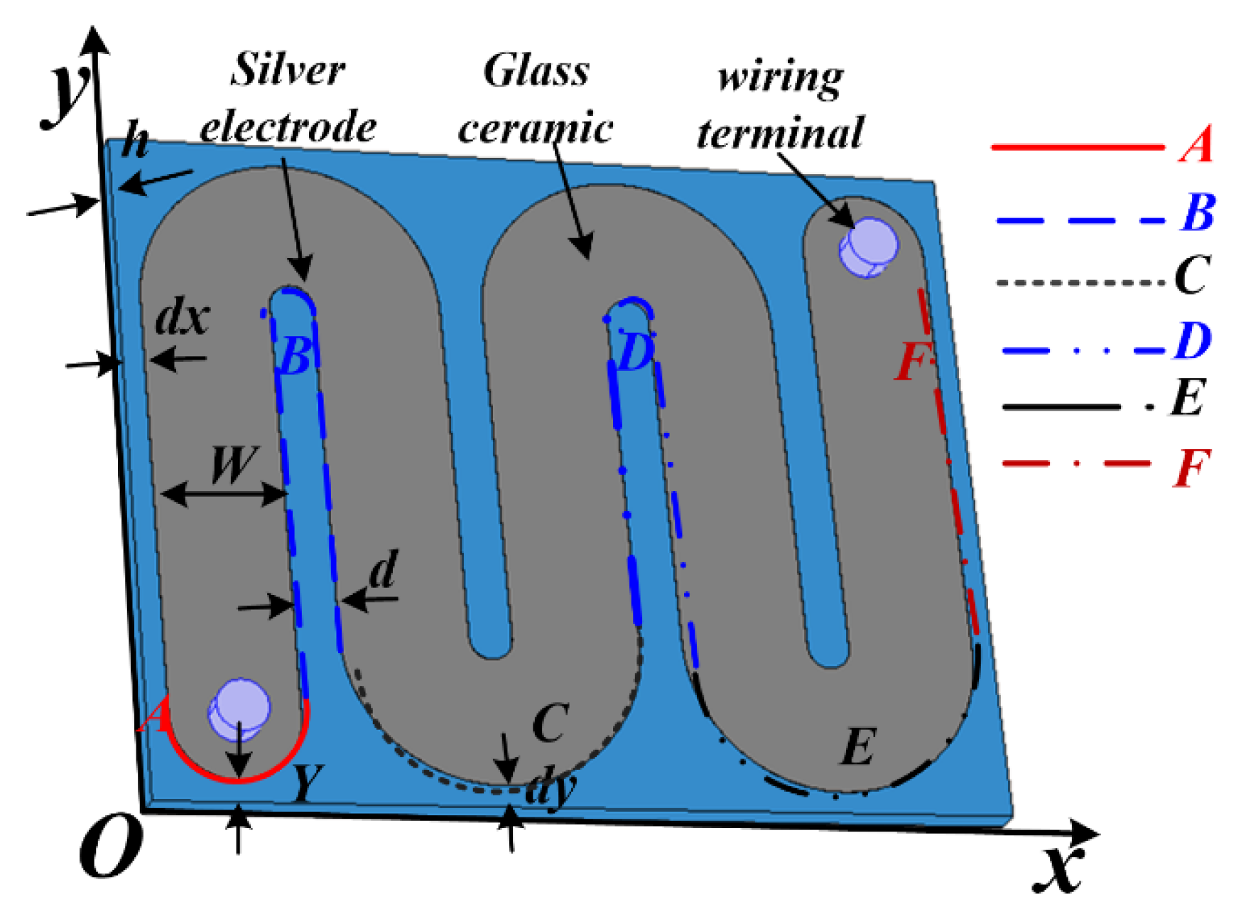
Figure 1 shows the structure of the PFL, which is composed of glass–ceramic material, high-voltage and ground electrodes, wiring terminals, and packing material. The four wiring terminals are located at the ends of the zigzag high-voltage electrode and the relative position of the ground electrode. The packing material is coated around the ceramic material and electrodes to reduce surface flashover and avoid possible bumps. The main structural parameters include dielectric thickness
h, electrode width
W, spacing between straight line of the electrode
d, margins between edges of electrode and ceramic material
dx/
dy, and locations of the wiring terminals
Y.
Key parameters of the PFL are presented in
Table 1.
In order to reduce the edge field enhancement, characteristics of the zigzag high-voltage electrode, including spacing between the straight line of the electrode (
d), margins between the edges of electrode and ceramic material (
dx,
dy) at different directions, and locations of the wiring terminals (
Y), were studied and optimized as shown in
Figure 1, numerically.
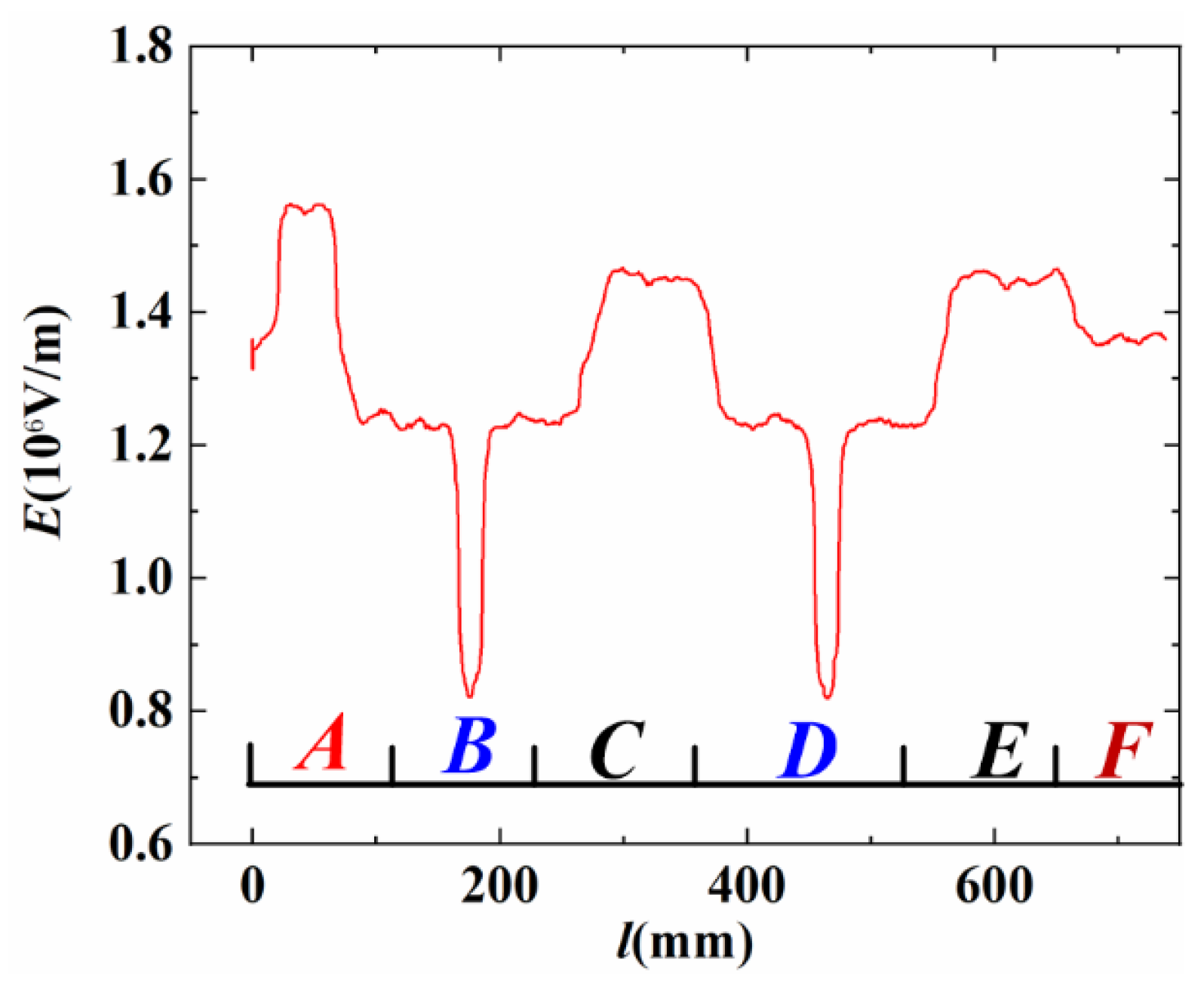
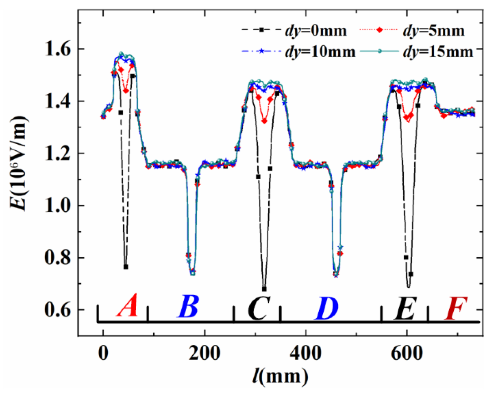
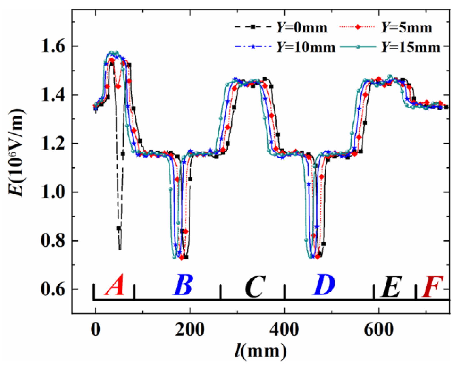
Finite-element analysis software COMSOL was used to analyze electric field distribution along the edge of the zigzag high-voltage electrode. The simulation was carried out under conditions with open boundaries. A voltage of 35 kV was applied on both sides of the PFL to monitor the electric field intensity of line segments A, B, C, D, E, and F on the electrode surface, and the electric field was achieved as shown in
Figure 2.
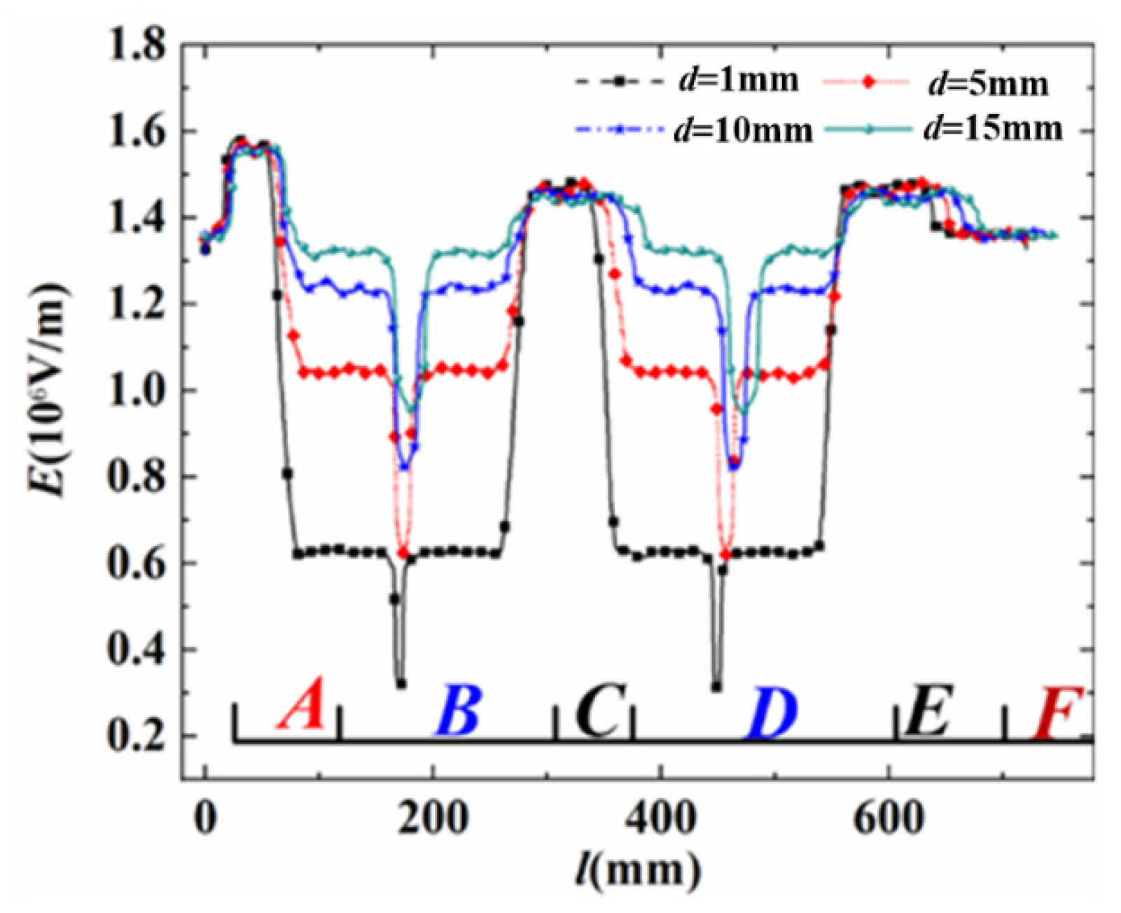
2.1. Spacing Between Straight Line of the Electrode
It can be seen that with the increase in the spacing between the straight line of the electrode
d, the field strength of line B and D in the figure (corresponding to the two depression positions in
Figure 1) continues to increase, and the field strength of other positions is basically unchanged. The surface field strength is weakest at the B and D segments of the entire electrode surface, and the field strength at the B and D segments does not change the maximum field strength of the entire electrode surface. Nevertheless, it is also necessary to reduce the field strength at the B and D segments as much as possible to prevent electrode breakdown at the B and D segments. As the spacing between straight line of the electrode varies from 1 mm to 15 mm, the electric field on line B and D increases from 0.62 kV/mm to 1.35 kV/mm, shown in
Figure 3. As for full utilization of the limited cross-section of the glass–ceramic material, spacing between the straight line of the electrode should be smaller; however, the electric potential along the zigzag high-voltage electrode is different during the transient process for pulse modulation. Considering the possible flashover on the surface of the material, the value is set to 5 mm.
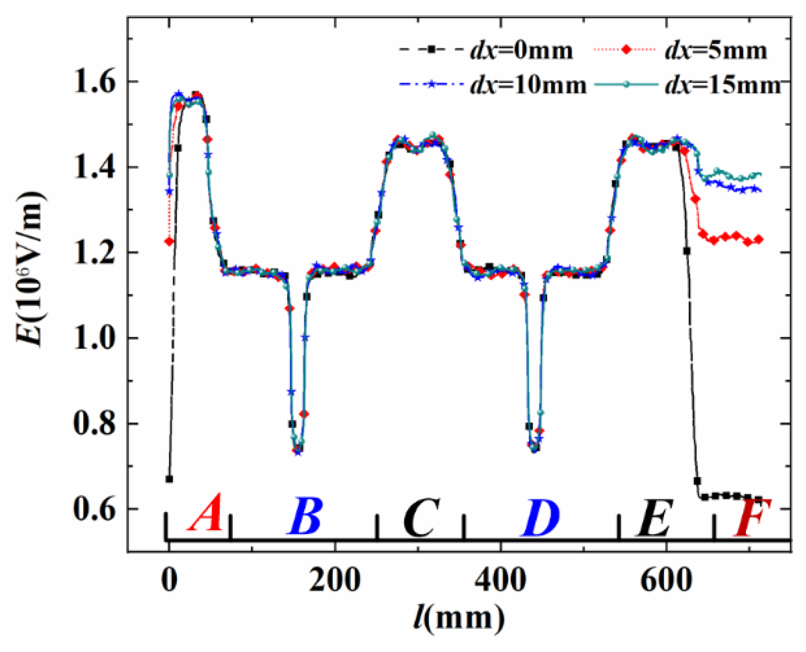
2.2. Margins Between Edges of Electrode and Ceramic Material
The electric field near the region of the edge of the ceramic is more complex for the discontinuity of the material. Accordingly, the possibility of the flashover is higher.
It can be seen that with the increase in dx/dy in the x/y direction, the field strength of line segment A and F in the figure (corresponding to the left and right positions in
Figure 1) continues to increase, and the field strength of other positions is basically unchanged. By reducing
dx/
dy in the
x/
y direction, the surface field strength of the electrode can be reduced, so as to improve the breakdown voltage.
As the margin between the edges of the electrode and ceramic material in
x direction changes from 0 mm to 15 mm, the electric fields on line A and F vary from 0.63 kV/mm to 1.4 kV/mm, as shown in
Figure 4. It is clear that when the d
x is set to 0 mm, the electric field is only 0.63 kV/mm.
As the margin between the edges of electrode and ceramic material in y direction changes from 0 mm to 15 mm, the electric field on line A, C, and F varies from 0.66 kV/mm to 1.5 kV/mm, shown in
Figure 5. Setting dy to 0 mm seems better.
2.3. Locations of the Wiring Terminals
The location of the wiring terminal can influence the field distribution of the PFL. As shown in
Figure 6, when the distance between the wiring terminal and margin of the ceramic material at y direction varies from 0 mm to 15 mm, the electric field on line A increases from 0.72 kV/mm to 1.55 kV/mm. The reason is that as the distance increases, the adjacent zigzag electrode can provide possible shielding for the field near the wiring terminal. According to the simulation results, 0 mm was selected.
The simulation results show that the surface field strength can be reduced by reducing the spacing between straight line of the electrode d, dx/dy in the x/y direction, and the locations of the wiring terminals Y. Theoretically, the breakdown voltage can be increased, so that the service life of the PFL can be improved under the same operating voltage.
3. Experiment Study on the PFL
3.1. Development of the PFL
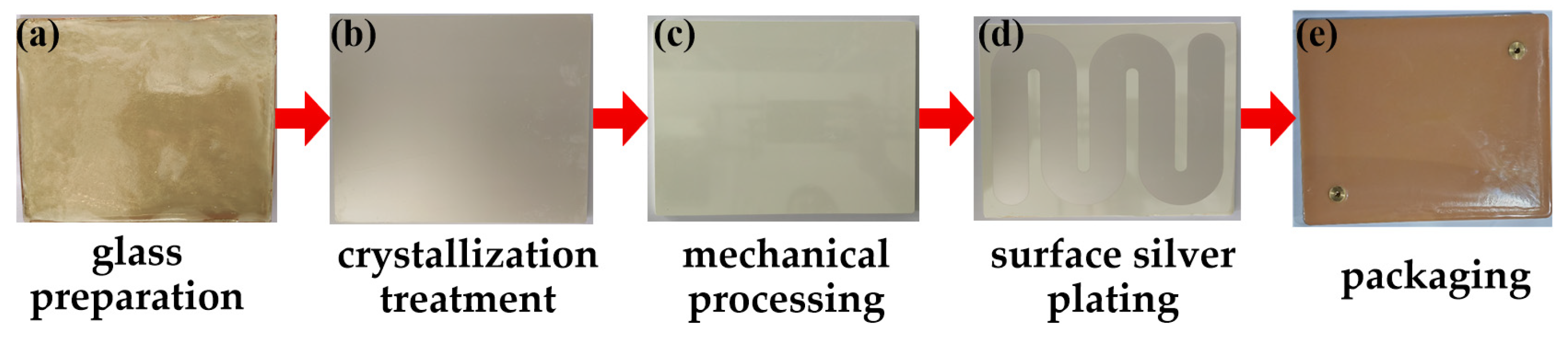
The development process of the PFL is shown in
Figure 7. It mainly includes glass preparation, crystallization treatment, mechanical processing, surface silver plating, packaging, and so on.
(a) Glass preparation
The preparation of glass generally involves three processes: the preparation of glass melt, the shaping of block glass, and the stress-relieving annealing.
(b) Crystallization treatment
The ceramic phase in glass ceramics is formed by crystallizing the granular glass. The crystallization treatment is generally divided into two stages. In the first stage, the glass is heated to a certain temperature for nucleation formation and held for a period of time to ensure the formation of a large number of uniform nuclei; in the second stage, it is heated to a certain temperature for crystal growth and held for a period of time to allow the nuclei to grow uniformly, resulting in glass ceramics with sub-micron or even nanometer size.
(c) Mechanical processing
After crystallization treatment, the surface of the glass ceramic has micro protrusions and is relatively uneven. Therefore, it is necessary to polish the surface to reduce the surface field strength and enhance the compressive strength.
(d) Surface silver plating
After coating the ceramic surface with silver paste, it is heated in a high-temperature furnace. To ensure the uniformity and flatness of the surface silver electrodes, multiple printing methods are adopted.
(e) Packaging
The PFL is placed into a fixed mold, epoxy resin added, and then it is put into a vacuum-drying oven for vacuum treatment. After degassing, curing treatment is performed.
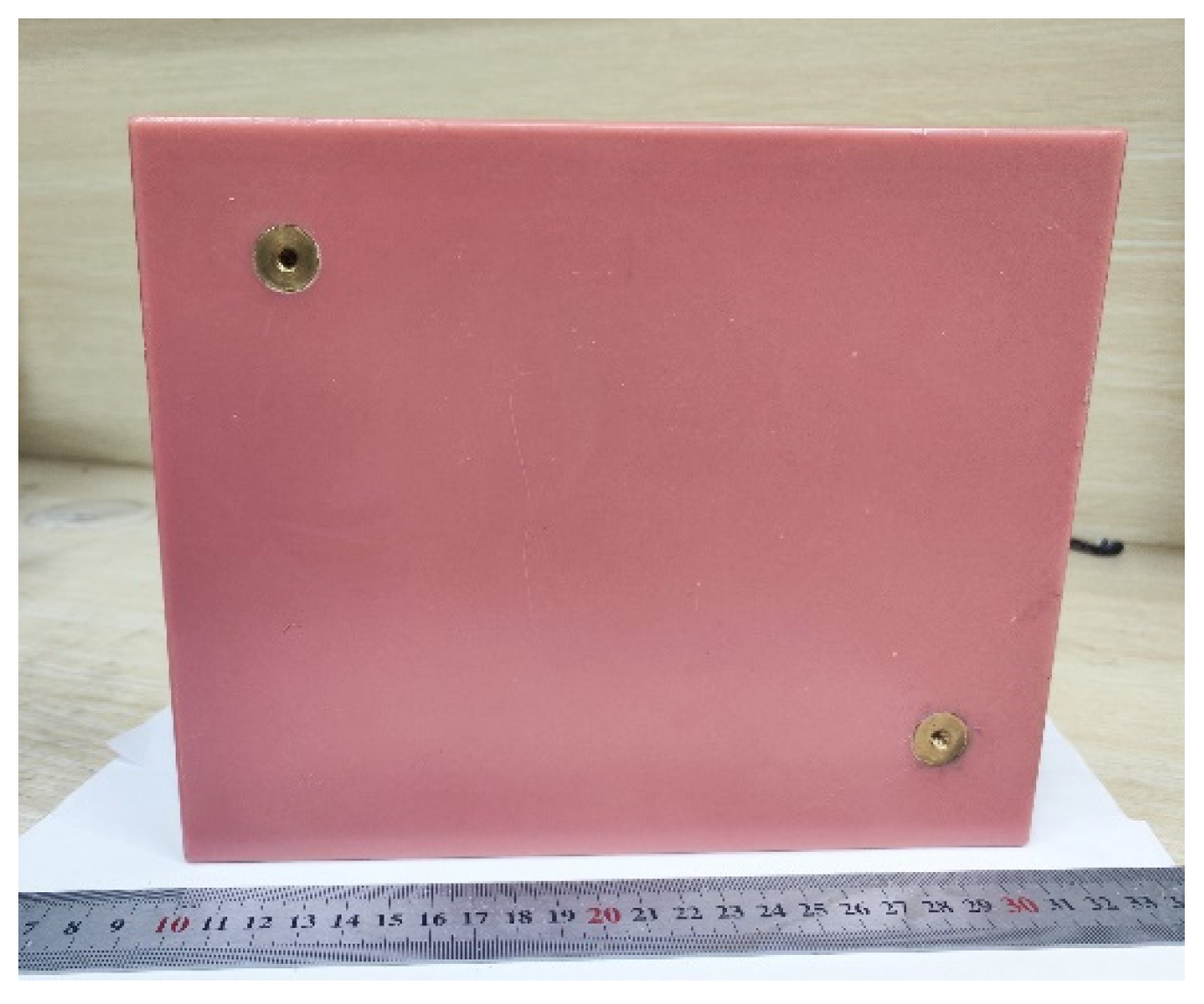
The PFL was built in our laboratory as shown in
Figure 8. The weight of the PFL is only 2 kg.
3.2. Low-Voltage Pulse Transmission
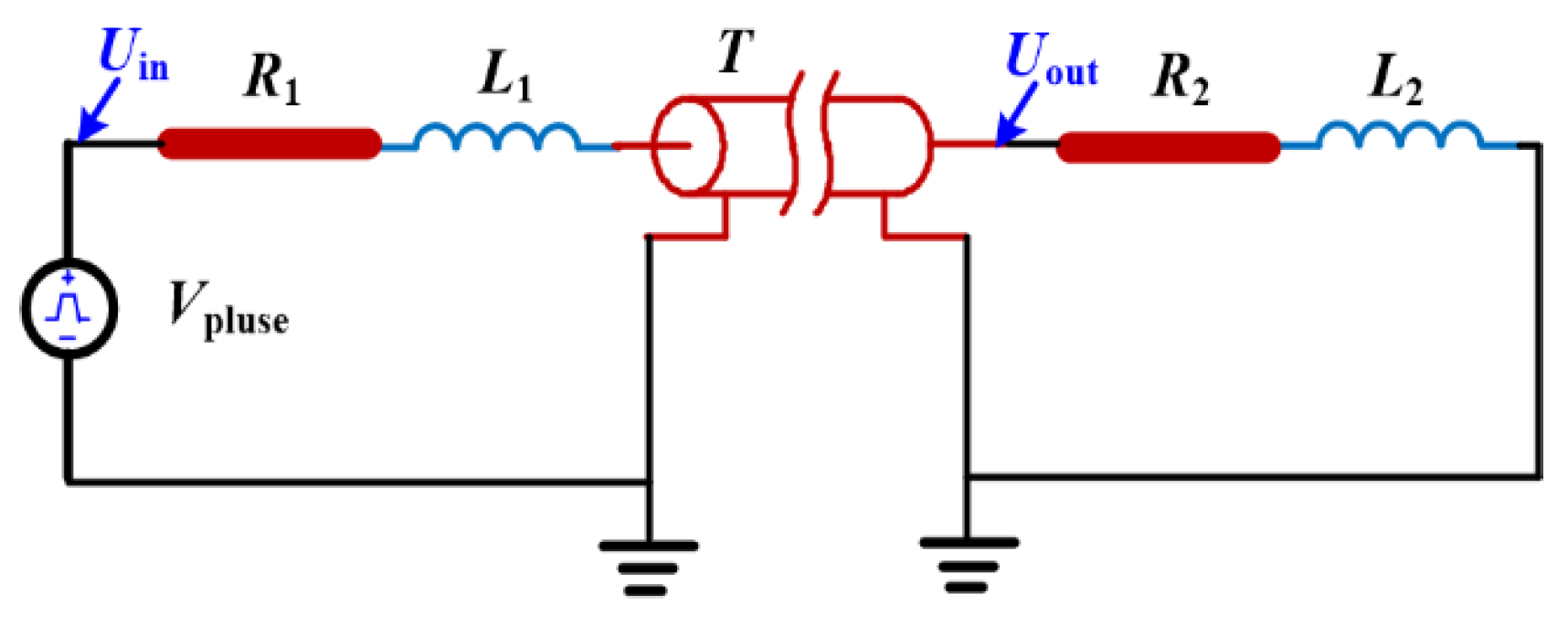
A transmission test of the PFL was carried out with low-voltage quasi-square pulse, numerically and experimentally. The circuit of the test, shown in
Figure 9, was developed with P-Spice software and numerical studied. A quasi-square wave signal
Uin is fed to one port (input end) of the PFL through a signal generator, and a resistive load is connected to the other port (output end). When the quasi-square wave signal is transmitted from the input end to the output end, the output end outputs a quasi-square wave signal
Uout. The pulse delay time between
Uin and
Uout is the electrical length of the PFL.
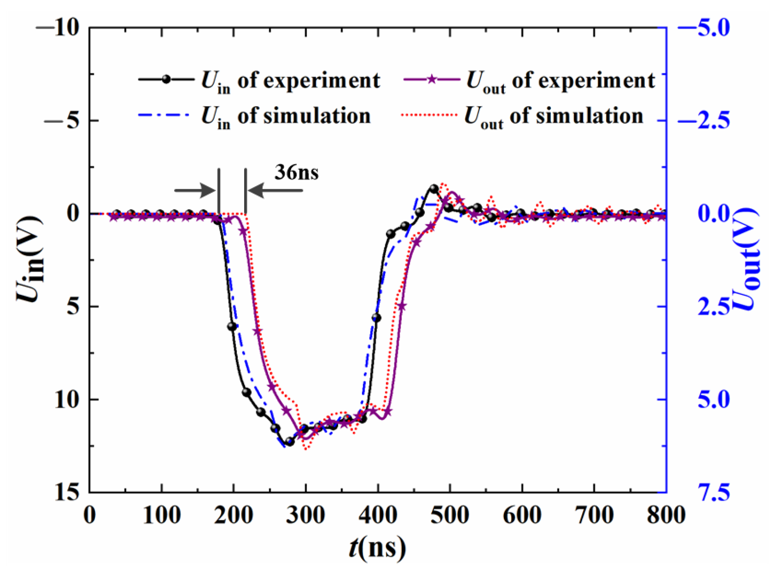
Results of the input and output pulses are shown in
Figure 10 (in solid line). It is clear that the output pulse with a signal delay of 36 ns was obtained approximately on a matched load. The circuit is built in the laboratory. A low-voltage signal source gives a 200 ns square wave signal feeding to the PFL and the experiment results on the matched load were shown in
Figure 10 (in dotted line). It can be seen that the results are in reasonable agreement with each other. The distortion of the pulses may come from varying parameters in the circuit, which is more obvious in low-impedance PFL.
3.3. Low-Voltage Pulse Modulation
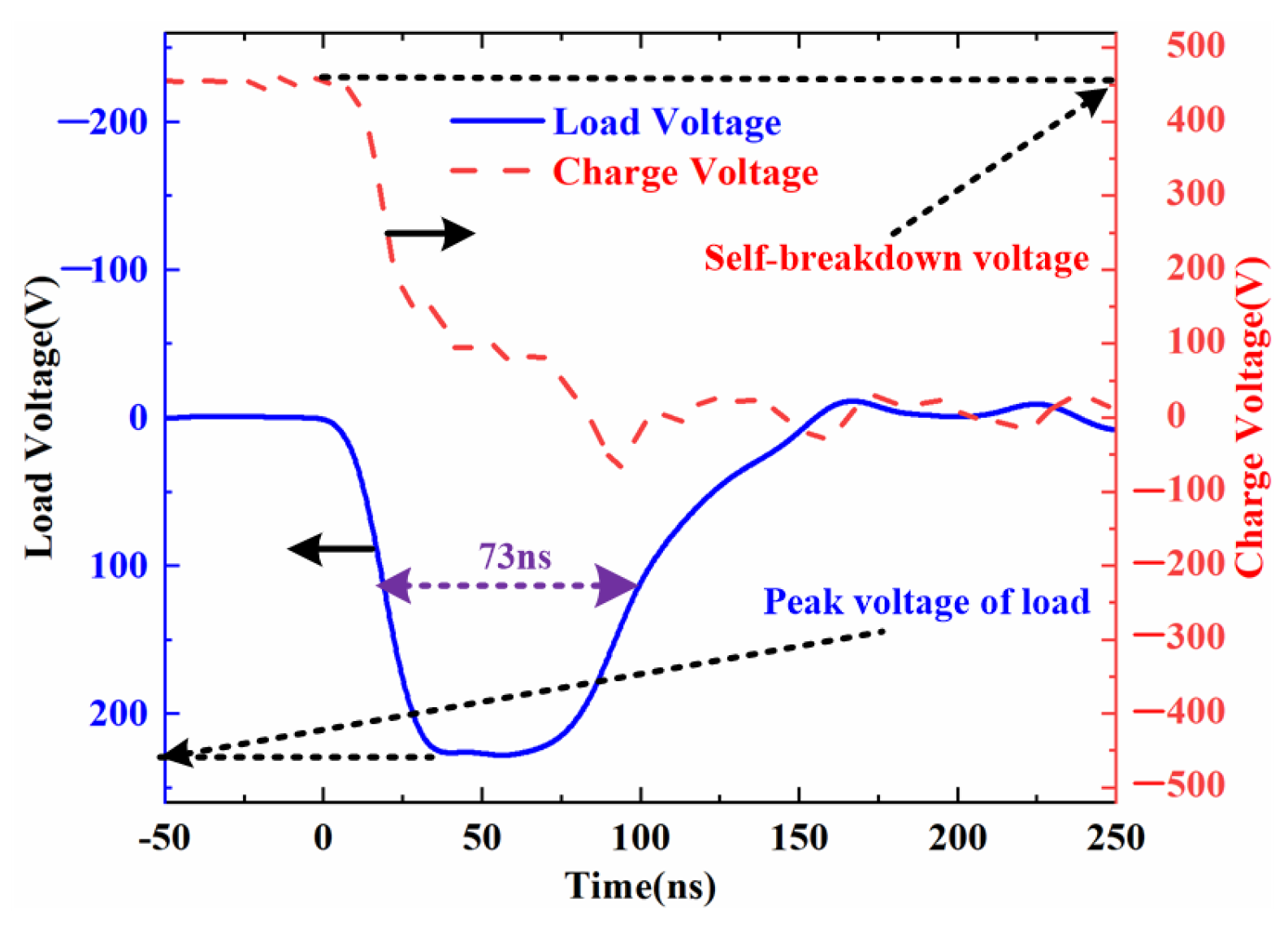
A low-voltage experimental platform was built with a mechanical switch. Typical voltages are shown in
Figure 11. It is shown that as the PFL is charged to 520 V, the switch is turned on, and a quasi-square pulse is generated with voltage of 262 V and duration of 73 ns, which meets the theoretical and numerical results.
3.4. High-Voltage Pulse Modulation
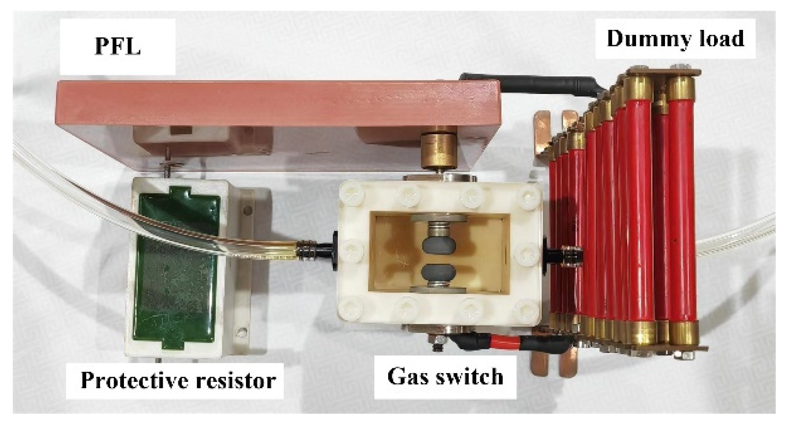
The high-voltage experimental platform, including high-voltage DC source, protective resistor, the PFL, spark gap switch, and dummy load, was developed according to
Figure 12. The working process can be described as follows. Initially, the PFL is charged by the DC source in constant current in 20 ms. As the voltage on the PFL approaches approximately 35 kV, the spark gap switch is turned on, and the energy is released to the load resistor. In order to keep a relatively low inductance in the discharge circuit, the distance between electrodes is small, and the breakdown voltage is adjusted by varying the gas pressure.
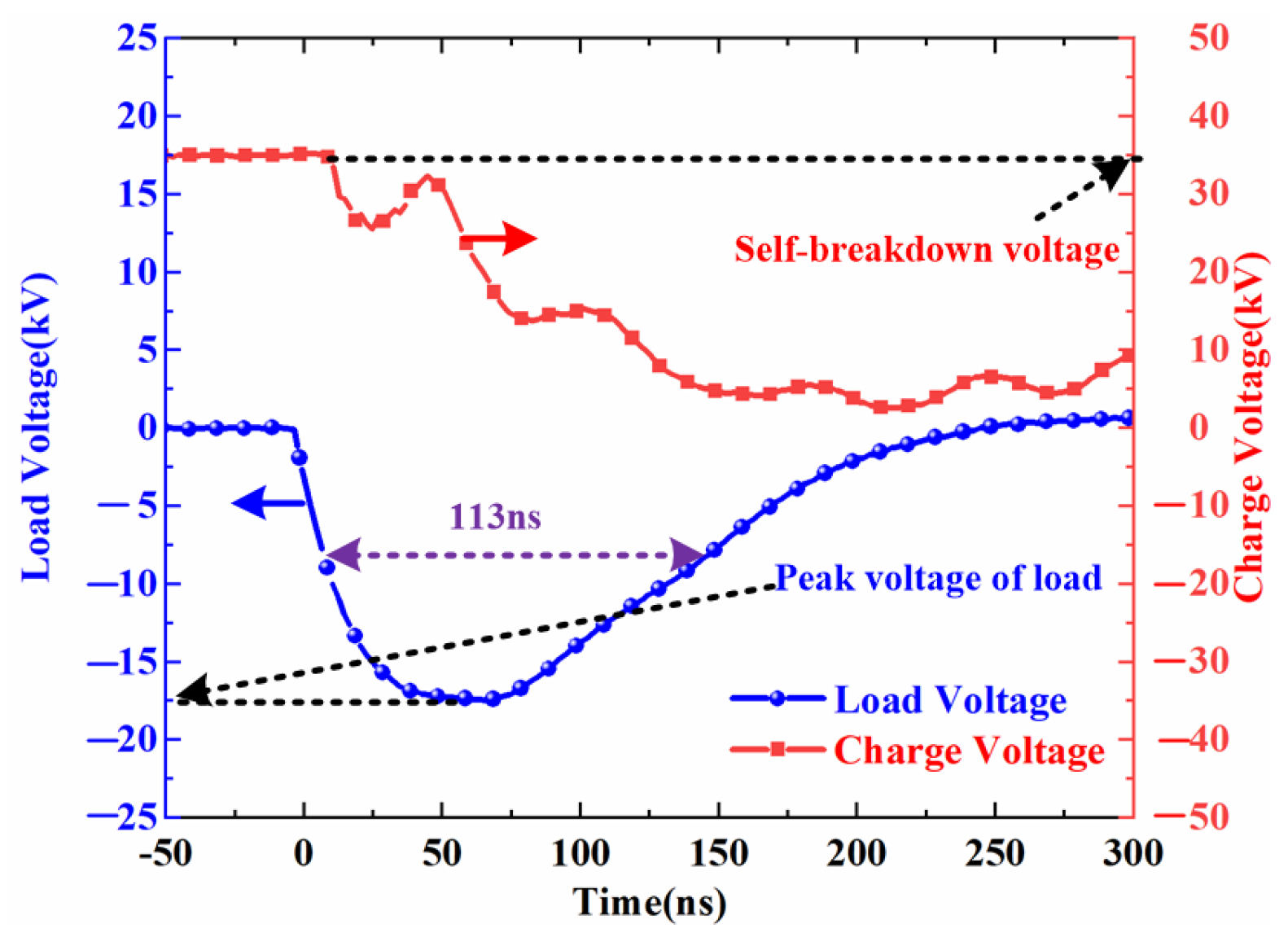
Typical voltages on the PFL and the dummy load were shown in
Figure 13. It can be seen that a quasi-square pulse with peak voltage of 17.6 kV and duration of 115 ns was achieved when the charging voltage is about 35 kV. The increase in the duration is due to the impedance mismatch, high inductance in discharge circuit, and depolarization characteristics of the glass ceramic during the fast energy discharge.
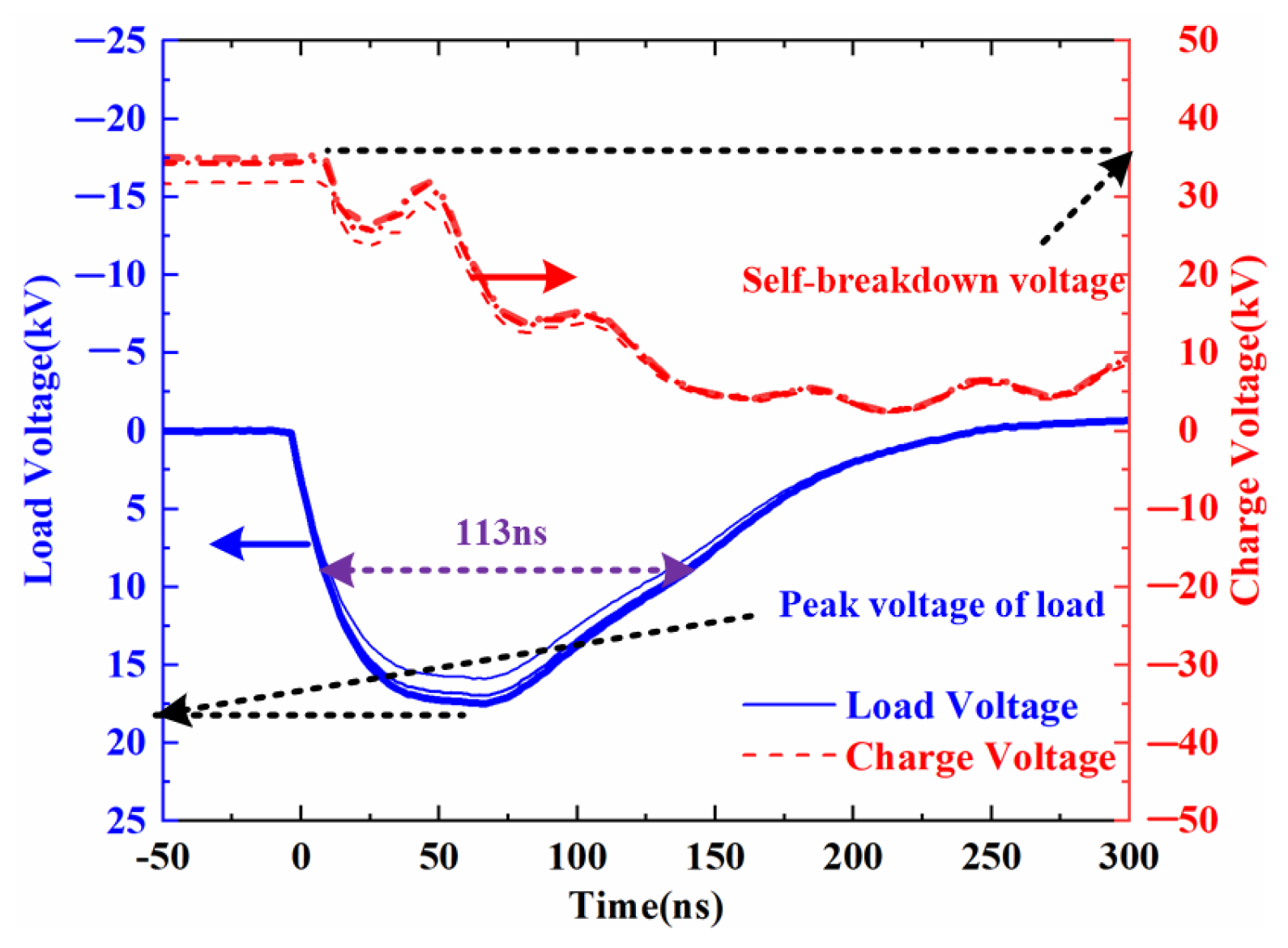
Figure 14 shows the performance of the PFL working in a charging voltage of 35 kV and repetitive rate of 50 Hz, which contains 1000 waveform superimpositions, and the dispersion of breakdown voltage is 1.5%. The results show that the reliability of the PFL is good. The PFL has the ability to operate stably for a long time. It was operated for 2.8 million times at 35 kV voltage, and the waveform was basically the same as that in
Figure 11. Compared with the 800,000 times shown by the similar PFL reported previously [
15], its life is increased by about 2.5 times.
4. Discussion
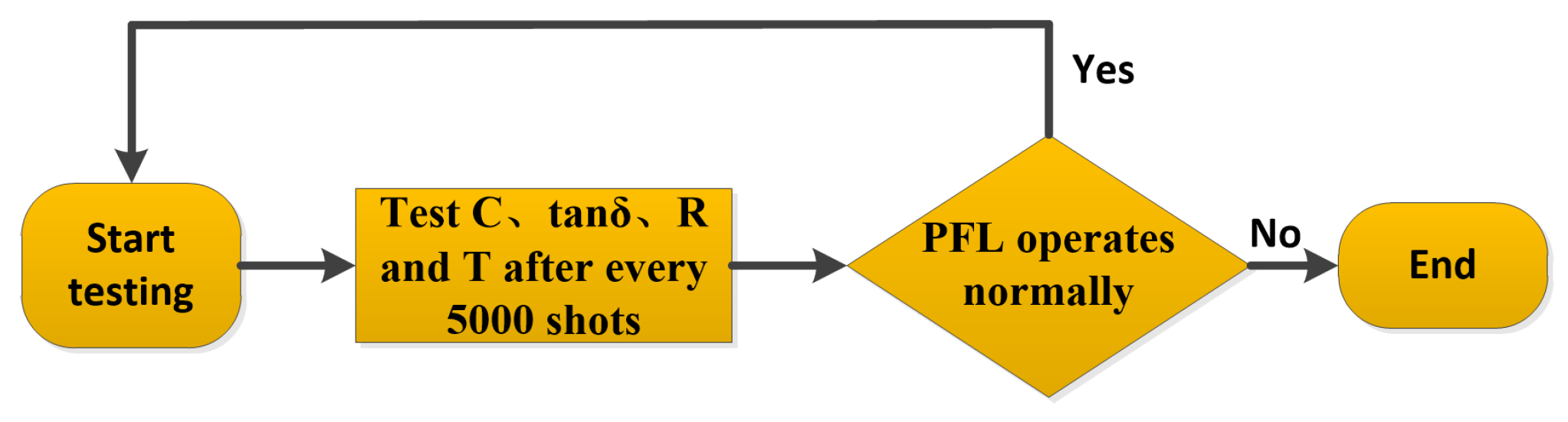
The lifetime test of the PFL was conducted on the experimental platform shown in
Figure 11. The PFL was operated in a charging voltage of 35 kV, and the repetitive rate was 50 Hz. After 5000 pulses of each experiment, the capacitance value, tangent of the loss angle, and leakage resistance of the PFL were measured using an LCR meter, and the surface temperature changes of the PFL were observed using a thermal imager.
Figure 15 shows the test flowchart of the PFL lifetime. Currently, the PFL has operated 2.8 million times and is still functioning normally.
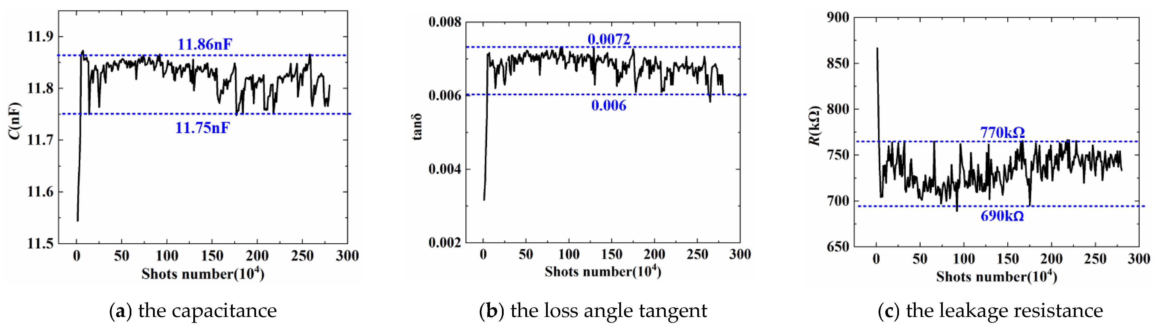
Figure 16 shows the capacitance, the loss angle tangent, and the leakage resistance of the PFL during 0 to 2.8 million pulses. Values of the PFL were measured every 5000 shots.
It can be seen in
Figure 16a that the capacitance of the PFL ranges from 11.55 nF to 11.85 nF after about 100,000 pulses. In the subsequent 2.7 million experiments, the capacitance of the PFL was basically between 11.75 and 11.86 nF, with a variation rate of less than 0.9%. The reason for the relatively large increase in the capacitance value of the PFL in the first 100,000 shots might be that the electrode surface was not stable at the beginning, with slight protrusions and sharp tips. After 100,000 shots for aging, the surface conduction channels became basically stable, so the capacitance value remained stable in the subsequent 2.7 million shots. In 2.8 million shots, the capacitance changes with the number of shots with a small amplitude (the change rate is less than 0.9%), so the characteristic impedance and pulse width of the PFL change is also small, and the output waveform stability of the PFL is good, indicating that the PFL has the ability to work stably for a long time.
In
Figure 16b, the loss angle tangent of the PFL remains at around 0.007 after 100,000 pulses. The loss angle tangent characterizes the ratio between the loss power PS and the lossless power PQ of the PFLs, and a smaller loss angle tangent indicates that the lower the loss power of the PFLs, the higher the energy utilization. The reason for the relatively large increase in the tangent value of the loss angle in the first 100,000 shots might be that there were no discharge channels around the electrodes at the beginning, and the overall power loss of the PFL was relatively small. As the number of shots increased, there might be ablation marks around the electrodes, increasing the power loss. After 100,000 shots, the ablation marks became relatively stable, and the power loss remained constant, so the tangent value of the loss angle remained stable. In 2.8 million experiments, the tangent value of the loss angle of PFL is very small and remains between 0.006 and 0.0072, indicating that the loss power of the PFL is small, and the PFL will not accumulate too much heat under long-term operation and has the capability of long-term stable operation with high frequency.
In
Figure 16c, it is clear that during 0 to 2.8 million pulses, the value stays at 690 kΩ to 770 kΩ. The leakage resistance can be used to measure the voltage resistance of the PFLs. The greater the leakage resistance, the better the voltage resistance of the PFL. After 2.8 million pulse experiments, the leakage resistance value of the PFL is always greater than 690 kΩ and remains between 690 and 770 kΩ, indicating that the PFL still has a strong voltage resistance after 2.8 million experiments and has the ability to work stably for a long time.
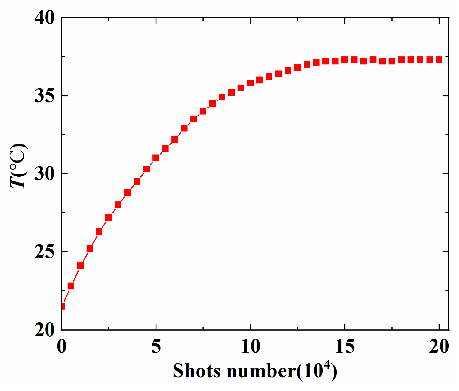
Figure 17 shows the variation in the maximum surface temperature of the PFL with shots number. The initial maximum surface temperature of the PFL is 21.5 °C. With the increase in the shots number, due to the internal loss of the PFL, the surface temperature keeps rising. At the same time, the PFL also dissipates heat to the external environment. It can be seen that the temperature rise amplitude of the PFL decreases continuously with the increase in the shots number; after 1.5 million shots, the PFL basically reaches thermal equilibrium, that is, the heat generated by the internal loss of the PFL is basically balanced with the heat transferred to the environment, and the maximum surface temperature of the PFL remains basically unchanged at 37.2 °C.
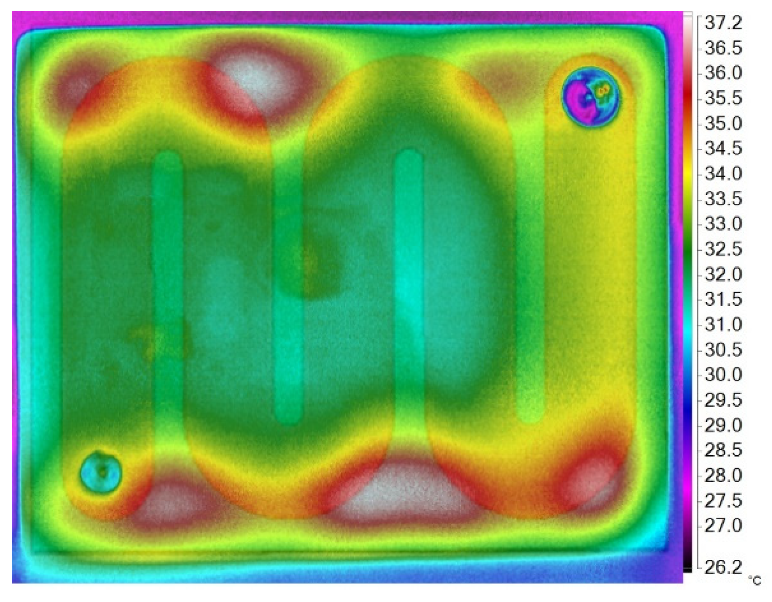
Figure 18 shows the surface thermal imaging map of the PFL after reaching thermal equilibrium. It can be seen that the surface temperature distribution of the PFL is uneven, varying from 26.2 °C to 37.2 °C. The maximum temperature of the PFL is located at the tip protrusion, corresponding to the area with the maximum electric field intensity (corresponding to lines A, C, and E in
Figure 1). The greater the electric field intensity, the easier electrons are to be emitted in all directions, and the more likely the ceramic surface is to undergo surface flashover along the surface, resulting in energy accumulation. With the increase in the number of experiments, the accumulated heat increases, and the temperature also rises. During the experiment, the temperature of the PFL always remains between 20 °C and 40 °C. According to the research results of the temperature characteristics of the PFL, within this temperature range, the electrical parameters of the PFL can remain stable, ensuring that the PFL can operate stably for a long time.
The lifetime of the developed PFL can reach more than 2.8 million times under the charging of 35 kV and repetition frequency of 50 Hz, which is about 2.5 times longer than the 800,000 times reported for a similar PFL in [
14]. Moreover, its capacitance, loss angle tangent value, and leakage resistance can remain stable. The variation rate of the capacitance of the PFL is less than 0.9%, which ensures that the characteristic impedance and pulse width of the PFL remain basically unchanged. The tangent value of the loss angle is always less than 0.0072 and remains basically stable, with low power loss, ensuring that the PFL does not accumulate excessive heat during long-term operation and possesses the ability to work stably for a long time at high frequency; the leakage resistance remains above 690 kΩ, ensuring the long-term voltage tolerance of the PFL. This is of great significance to increase the stability of the pulsed power system.


