1. Introduction
Supplying and conditioning power are the most fundamental functions of an electrical system. In modern electronics, it is very important to adapt the voltage and current levels coming from an external source to a user with different voltage–current characteristics. As the use of battery-powered portable devices such as mobile phones, laptops, and various handheld devices has rapidly increased, power management should be one of the most important issues for maximizing the battery lifetime and providing energy to multiple on-chip blocks. Most electronic systems need a stable voltage to obtain performance in different operating conditions, especially in medical, military, and space fields [
1].
A voltage regulator is an integral part of the power management system (PMS) of all electronic devices, and it has been the focal point of research over the past few years [
2]. The main issues concerning the low-dropout (LDO) regulator design consist of noise minimization and robustness against parameter variations. There are many sources of intrinsic noise in LDO. The major types of intrinsic noise include thermal noise, 1/f noise, shot noise, and burst, or popcorn, noise. To suppress thermal and flicker noise, conventional LDOs utilize highly filtered voltage references at their inputs and bypass capacitors at their outputs [
3]. Traditional LDOs are often affected by noise from the active devices of bandgap reference (BGR) and error amplifier (EA), leading to poor noise performance at low frequencies [
4].
To minimize the LDO noise, different topologies have been investigated, for example, the reduction in noise incorporating a capacitance-amplifying circuit in the structure of an LDO with pre-regulation [
5]. Noise reduction by reducing the gain of error amplifier and RC filter could also achieve an ultra-low-noise LDO [
6]. Another method involves switched-RC filter at the output of the bandgap reference along with drain-side modulated current-mode on an output capacitorless LDO [
7]. A simple RC network reduces the noise within the amplifier by the increased
gm of the second stage and the noise outside the amplifier coming from the bias by low-pass filtering [
8]. Approaches such as chopper technology can also help improve noise performance [
9], but it only improves the noise from the operational amplifier. Some techniques to improve Power Supply Rejection (PSR) have also been proposed, such as feed-forward ripple cancelation (FFRC) [
10].
In this paper, a fully integrated low-dropout (LDO) regulator characterized by low noise performance and low power consumption, suitable for battery applications, is designed. To enhance performance, we employed a folded cascode operational amplifier (op-amp) with a class AB buffer, as the error amplifier (EA), in such a way as to obtain a low-dropout voltage, low noise, high efficiency, good transient response, and stability over a wide range of frequencies. The proposed LDO architecture introduces several key advancements over conventional designs. First, it employs a folded cascode operational amplifier with a class AB buffer as the error amplifier, significantly enhancing noise performance while maintaining high efficiency. Unlike traditional LDOs that rely on large external capacitors or additional filtering circuits, our design achieves low noise operation through an optimized internal compensation strategy. Additionally, the proposed regulator features a low-dropout voltage of 67 mV, ensuring minimal power loss and making it highly suitable for battery-powered applications. The design also demonstrates superior transient response, achieving a rapid settling time under load transitions up to 100 mA. Furthermore, it maintains stable operation across a wide temperature range (−25 °C to +125 °C) and varying input voltages (2.8 V to 4.8 V), ensuring robustness under diverse operating conditions. These enhancements make our LDO a highly efficient and compact solution compared to existing circuit topologies.
The paper is structured as follows:
Section 2 provides the noise analysis.
Section 3 covers the proposed LDO regulator design, compensation strategy, and the current limiter circuit. The results are presented in
Section 4. The simulations were conducted under various operating conditions, including different input voltages (2.8 V to 4.8 V), load currents (0 mA to 100 mA), and temperatures (−25 °C to 125 °C). The simulation results were obtained using the Cadence Virtuoso platform, with the 150 nm process design kit (PDK). The simulations included transient, AC, and DC analyses, set up and run within the Analog Design Environment (ADE) of Virtuoso. The PDK provided the necessary models and technology files to ensure accurate and reliable simulation results.
2. Noise Analysis and Characterization in LDO Design
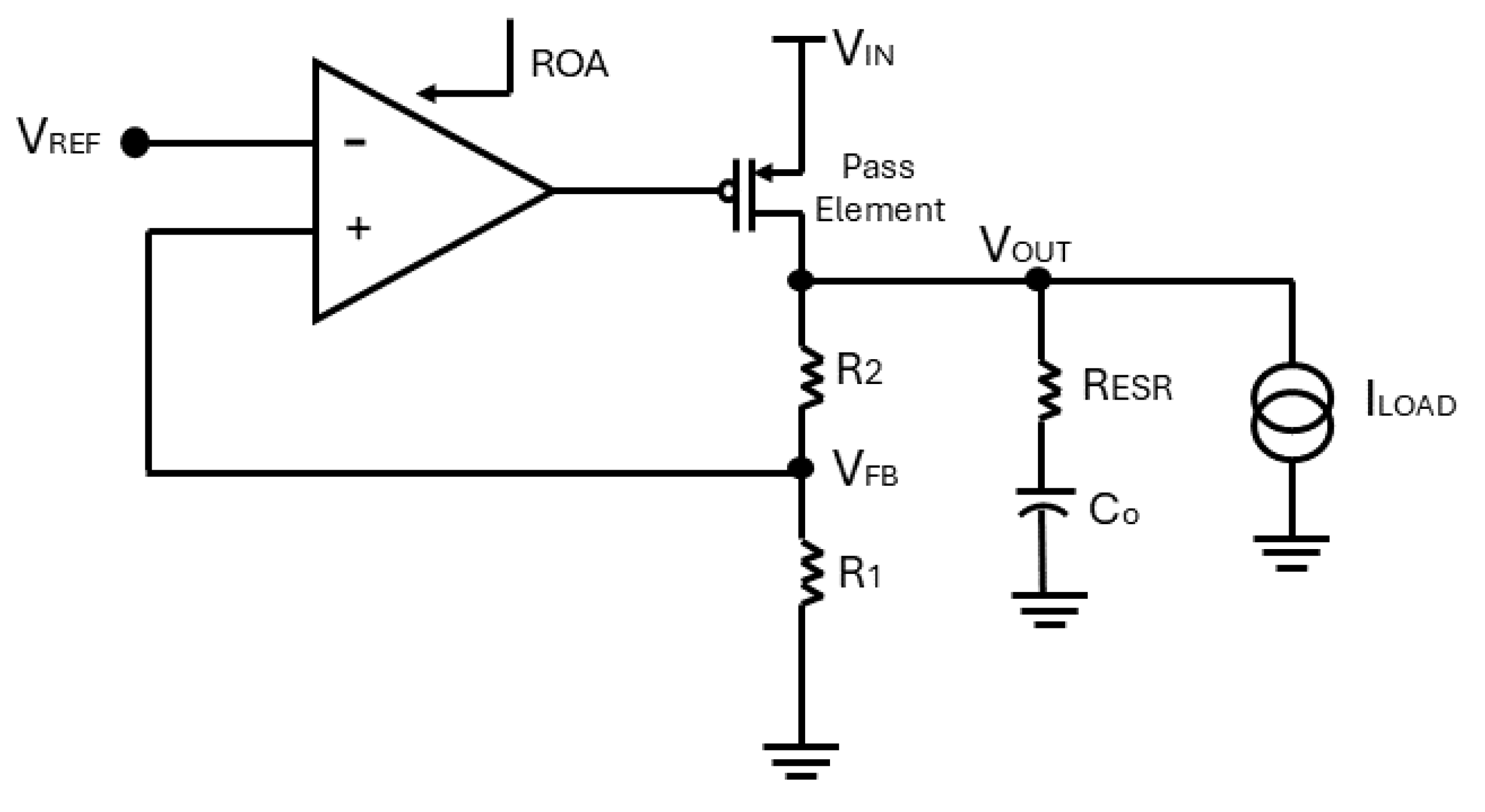
A conventional low-dropout voltage regulator (LDO) is presented in
Figure 1. The purpose of this work is to design a low-drop regulator with low noise specifications to provide its final user a stable independent and regulated voltage with changing output loads [
11]. The output voltage 2.6 V was selected based on the target application, which involves low-power battery-operated systems. Many modern portable devices often utilize lithium-based batteries, which have a nominal voltage of 3.7 V and discharge over time to lower voltages. The 2.6 V output is within the operational voltage range for these devices, ensuring efficient power delivery while maintaining sufficient headroom for proper functionality.
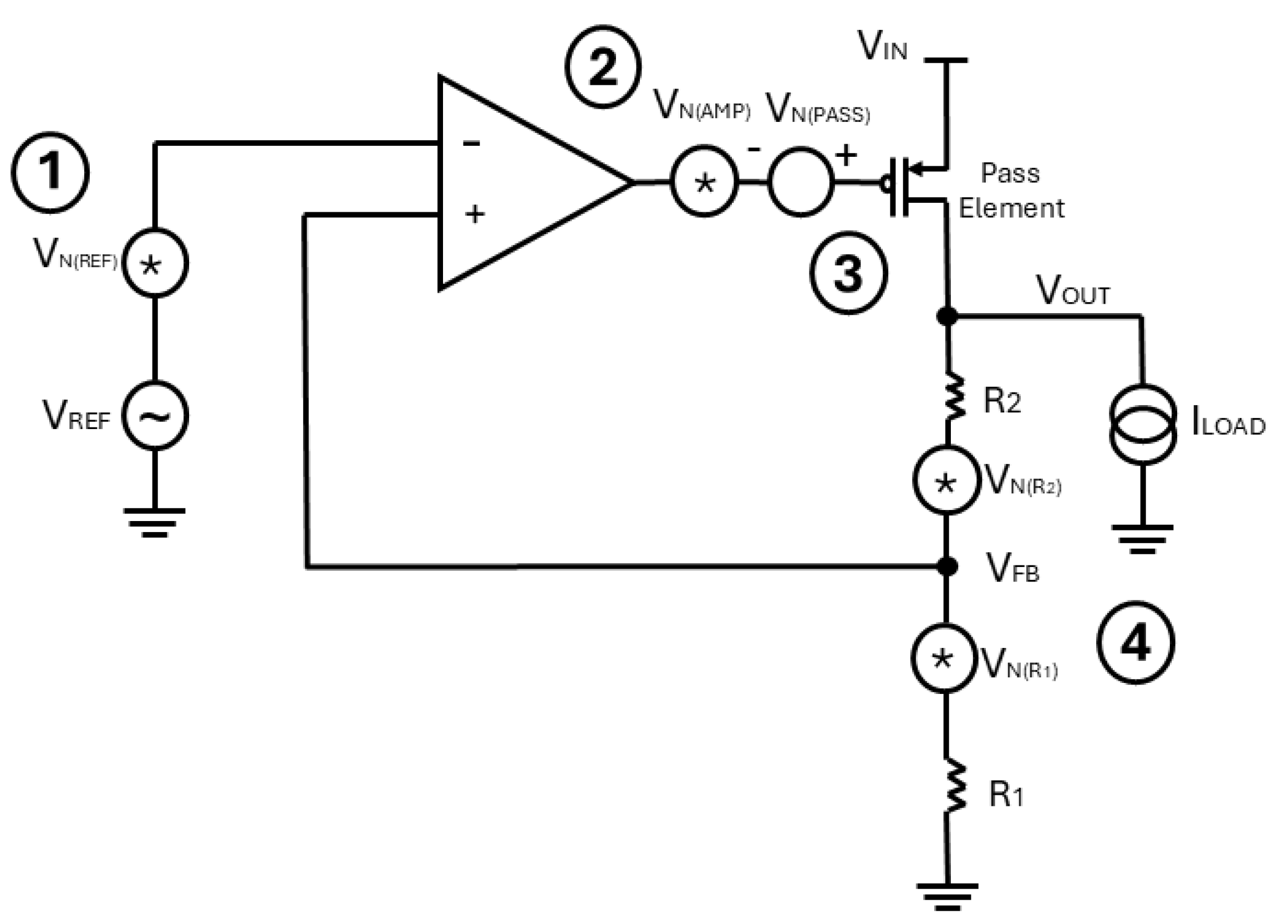
The Noise in an LDO is a frequency-dependent parameter. Many types of noise affect the output voltage, but mainly flicker noise contributes a major portion at low frequencies. The output noise voltage is the RMS value of noise voltage over the range of frequencies. Most of the output noise is caused by internal voltage reference and operational amplifier. Noise occurs in transistors and resistors and is considered a physical phenomenon. Mainly, transistors consist of flicker and shot noise. Thermal noise is generated by the resistive elements in a MOSFET. Thermal and shot noise noises do not depend on frequency [
12]. The noise in an LDO is originated from four major sources [
13]:
- 1.
Voltage reference;
- 2.
Error amplifier;
- 3.
Series pass element;
- 4.
Resistor divider.
The major contribution of intrinsic noise in LDOs is from voltage reference and error amplifier. The major noise sources are shown in
Figure 2.
The noise in an LDO can be expressed as a function of five sources:
where
is the output noise of LDO,
is the output noise of op-amp,
is the noise from reference voltage,
is the noise from the pass element, and
is the noise from the resistor ladder [
14].
3. Proposed LDO Regulator
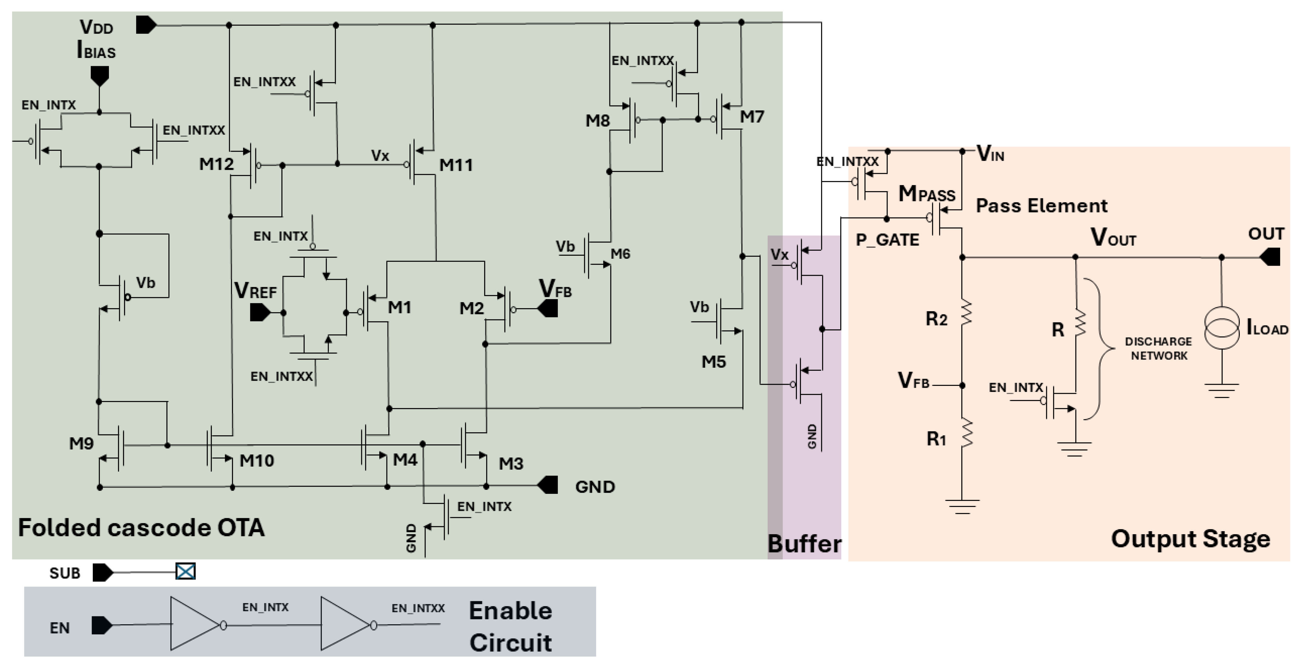
The complete schematic of the proposed LDO regulator is shown in
Figure 3. The circuit presents an LDO loop that was improved by adding a folded cascode error amplifier (EA) and Class AB buffer, particularly designed to provide sufficient flexibility to optimize op-amp stability. Given an external bandgap reference
= 1.2 V, to achieve an output voltage of
= 2.6 V with maximum load current of
= 100 mA and input voltage
ranging from 2.8 V to 4.8 V, the output capacitor Cout = 1
F with ESR 10 mΩ was added with the load. An internal compensation capacitor was also used, which facilitated the stability. The proposed LDO regulator was designed and simulated in a 150 nm standard CMOS process.
3.1. Output Stage
In
Figure 3, all devices are considered as 5 V thick-oxide transistors. When the PMOS
’s aspect ratio was fixed at (W/L)
= 10 mm/0.5
m, at maximum
= 100 mA and
= 200 mV, the LDO regulator’s dropout voltage is found to be
= 67 mV. Considering an output voltage
= 2.6 V and a reference voltage of 1.2 V, 1
A quiescent current was established.
The PMOS as the pass element was chosen due to its low noise applications. The aspect ratio (W/L) ratio was designed as described in
Table 1.
Since the dropout voltage was quite low, i.e., 67 mV, a wider pass element was selected to regulate the output voltage. The resistor values were selected to ensure precision in regulating the output voltage while keeping power consumption low. The values of
and
were designed using Equation (
2) to provide a minimum quiescent current:
where
is the output voltage,
is the external reference voltage, and
forms the resistor ladder. The resistor values were set to
= 100 kΩ and
= 167.67 kΩ, as a trade-off between power consumption and area. This choice resulted in a static current consumption of the output
branch
= 3
A.
3.2. Design of the Operational Amplifier
For the design of EA, folded cascode topology followed by a class AB buffer was chosen due to its high performance in terms of noise and stability. A folded cascode EA architecture has high gain, single pole, good noise performance, and a large output swing as compared to other architectures of error amplifiers.
The op-amp must operate properly for the input voltage range ( = 2.8 V–4.8 V). The bias current for op-amp was set to 1 A. and are a PMOS differential pair with identical transistors ensuring that = . The PMOS differential pair was chosen instead of NMOS due to its low noise performance.
represent the folded cascode topology, which converts the differential signal at the input into a single-ended type. current mirrors bias the folded cascode structure. , , , and establish the current mirrors for biasing the differential pair. The bias current of is set to 1 A. A follower buffer is employed after the operational amplifier. The operational amplifier, including the source follower buffer, consumes a total quiescent current of 4 A, which, when combined with the currents of the other branches, results in a total quiescent current of 5 A.
In
Figure 3, the green area represents the folded cascode topology, the purple area denotes the source follower buffer, and the pink area highlights the output stage of the LDO, while the gray area indicates the enable circuit, which has been incorporated into the design to enhance user convenience.
Table 2 shows the W/L selected for each MOSFET in op-amp.
3.3. Stability
The LDO loop contains two poles, which are associated with the output node and the gate of the pass element. The output pole, linked to the large output capacitor
F, serves as the dominant pole of the LDO. The second pole, resulting from the significant parasitic gate capacitance of the pass element, is shifted to a higher frequency by incorporating the source follower buffer [
15]. The buffer has been chosen with very low output impedance, so that the pole frequency is sufficiently high, thereby preventing it from contributing to the instability of the LDO [
16,
17].
The output capacitor
= 1
F with ESR = 10 mΩ constitutes the dominant pole of the LDO at the frequency given by Equation (
3):
where
is the output capacitor,
is the drain to source resistance of pass element,
is the series resistance of output capacitor, and
is the output load resistor.
The second pole, due to the output impedance of the op-amp and parasitic capacitance of the large pass element, is at
where
is the output impedance of the error amplifier and
is the parasitic input capacitance of pass transistor.
The zero is also introduced by the output capacitor at
where
is the output capacitor and
is the series resistance of output capacitor.
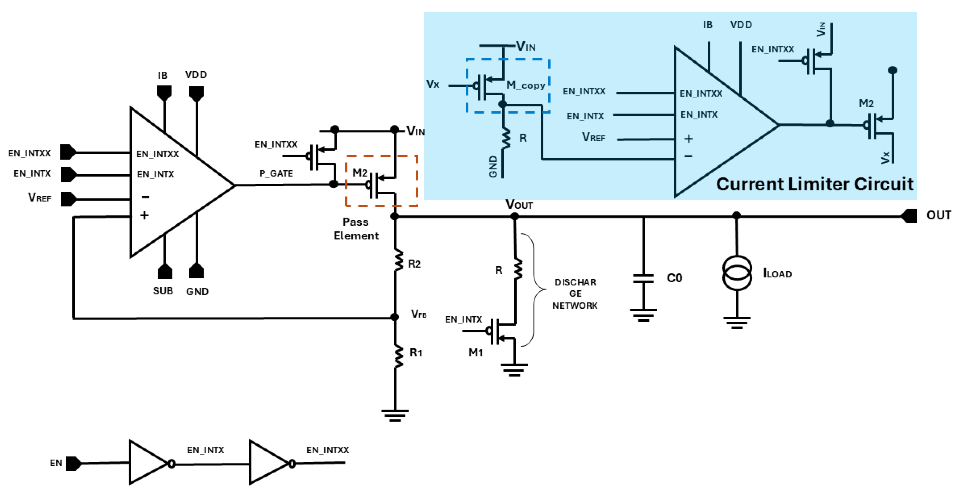
3.4. Short Limiter Protection
A current loop is introduced in the main circuit to protect against either of the following:
- 1.
Overshoots;
- 2.
Output shorted to the ground.
The current (
) is
(fraction of aspect ratios of pass element and copied pass element) times smaller than the pass current (
) and
is the drain current of the pass element. The size of PMOS has been selected to be smaller by a factor of a thousand than the pass element. The
is selected to be 160 mA by the following equation:
where
is the generated and reduced current for the short limiter circuit and
is the max drain current of the pass element, while
,
is the aspect ratio of pass element and copied pass element, respectively. In
Figure 4, the added short limiter protection is shown.
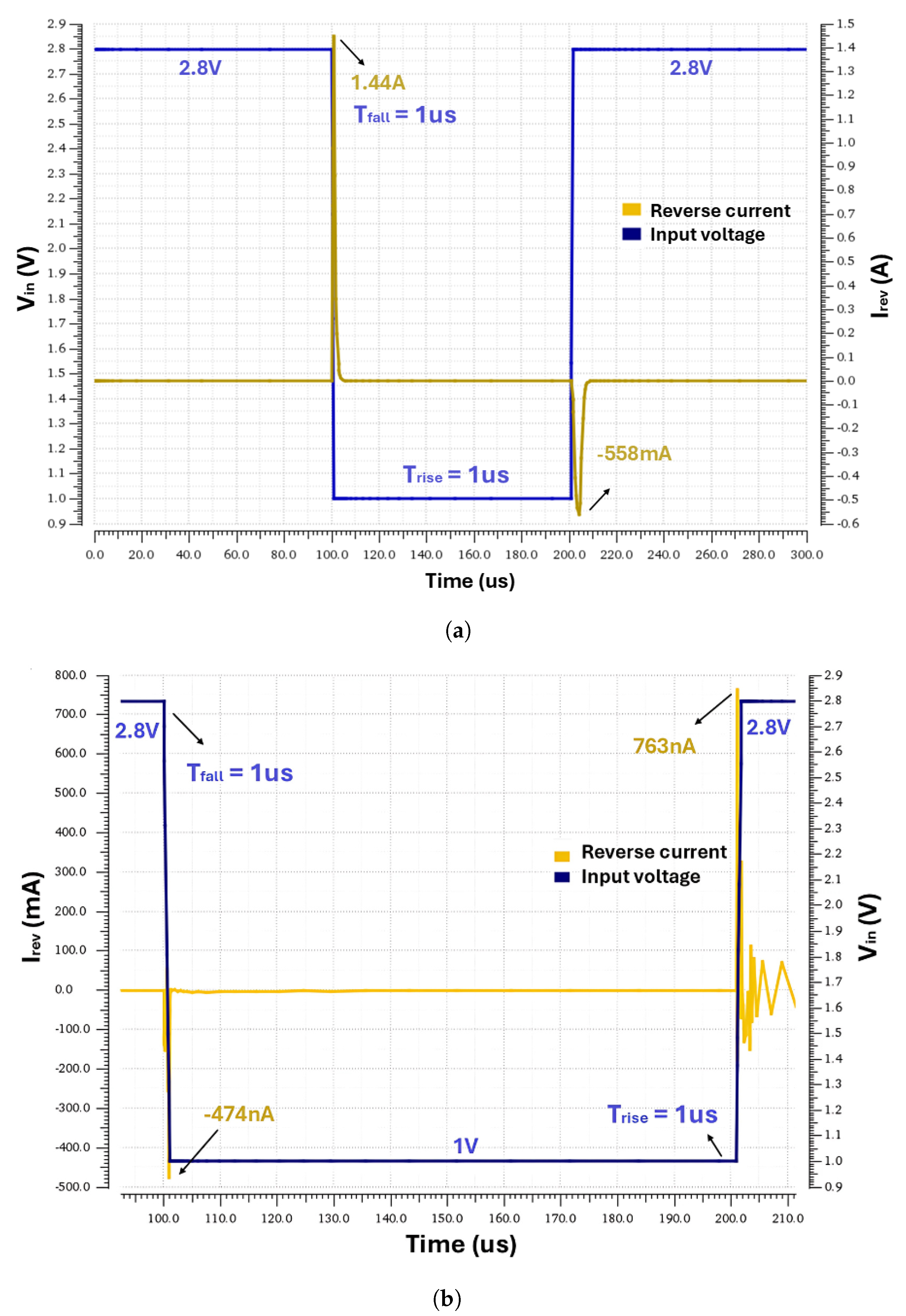
Without short limiter protection, the reverse current of the LDO would mirror the behavior illustrated in
Figure 5 and the overshoot current value reaching 1.44 A, which is not suitable for battery application. After the short limiter circuit was implemented, there was a notable decrease in reverse current. As shown in
Figure 5b, when
suddenly decreases from 2.8 to 1 V, the reverse current is restricted to −474 nA. The current after the short limiter circuit implementation always remains in the nA range. The short limiter circuit is crucial for circuits with a large output capacitor such as in our case with
1
F to enhance efficiency and to retrieve a low power consumption.
4. Results and Discussion
The designed LDO has been simulated at different operating conditions by sweeping input voltage, output load current, and temperature. The results obtained are discussed in detail.
4.1. Noise Performance
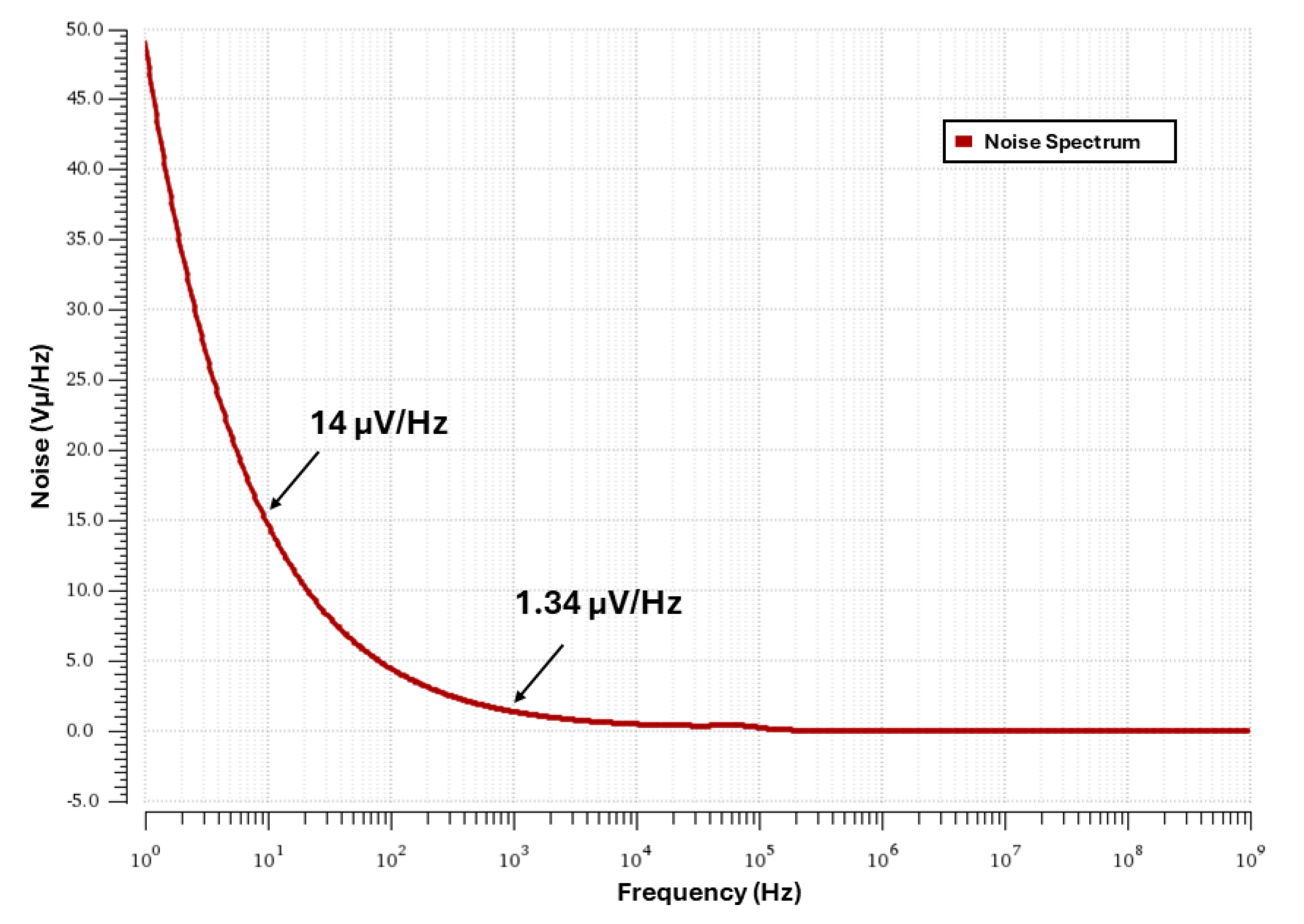
The primary focus of the evaluation in this manuscript was on the noise performance.
Figure 6 illustrates the output-referred noise spectrum of the LDO regulator, predominantly showing flicker noise between 1 Hz and 100 kHz frequencies. This finding is in line with expectations since flicker noise tends to dominate at lower frequencies. More precisely, the root mean square (RMS) noise is within the operational frequency range of the LDO regulator, which was found to be 14
@ 10 Hz, primarily contributed by the op-amp’s input differential pair and the current sources in the op-amp’s folded branch (refer to
Figure 4). In contrast, in [
6], an ultra-low-noise LDO regulator is presented, which employs two internal noise reduction networks at the output of the bandgap reference (BGR), i.e., a sample-and-hold switched-RC filter, and between output and feedback resistor nodes, which give rise to increase circuitry. A switched capacitor notch filter is utilized to filter out the residual chopping ripple of the error amplifier. These techniques reduce the total integrated output noise of the LDO in the 10 Hz to 100 kHz band from 95.3
VRMS down to 14.8
VRMS [
18]. Compared with the previous results, our LDO achieved good noise performance without additional circuitry.
4.2. Frequency Response
The simulated LDO’s frequency response, operating with a load current of 100 mA, input voltage of 2.7 V, and temperature T = +25 °C, demonstrates a phase margin of 46°, a gain of 121 dB, and a unity-gain frequency (UGF) of 17 kHz. This analysis evaluates the stability of the system at maximum load current. The unity-gain frequency (UGF) is 17 kHz, which demonstrates the stability of the LDO under maximum load current, as the UGF is sufficiently high to ensure robust performance across a wide range of operating conditions.
The proposed LDO achieves a gain-bandwidth product of 17 kHz and a phase margin of 46°, which ensures stability under maximum load current (100 mA). This is an improvement over the 10 kHz gain-bandwidth reported in [
18]. The use of a source follower buffer and internal compensation capacitor
shifts the second pole to a higher frequency, enhancing stability. The stability analysis under different load conditions (0 mA to 100 mA) shows that the phase margin remains above 37° even in the worst-case scenario (SSA corner at 125 °C), demonstrating the robustness of the design, as shown in
Figure 7.
4.3. Transient Response
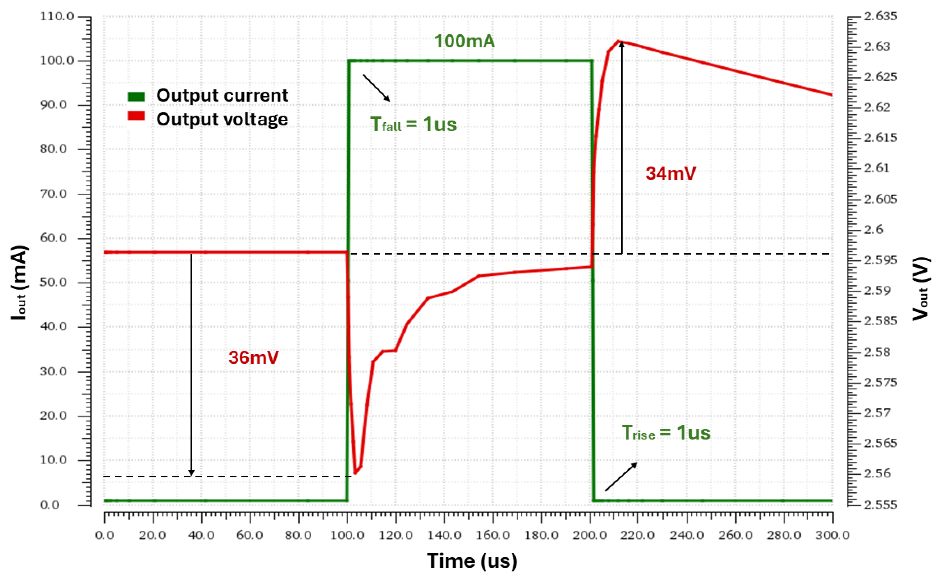
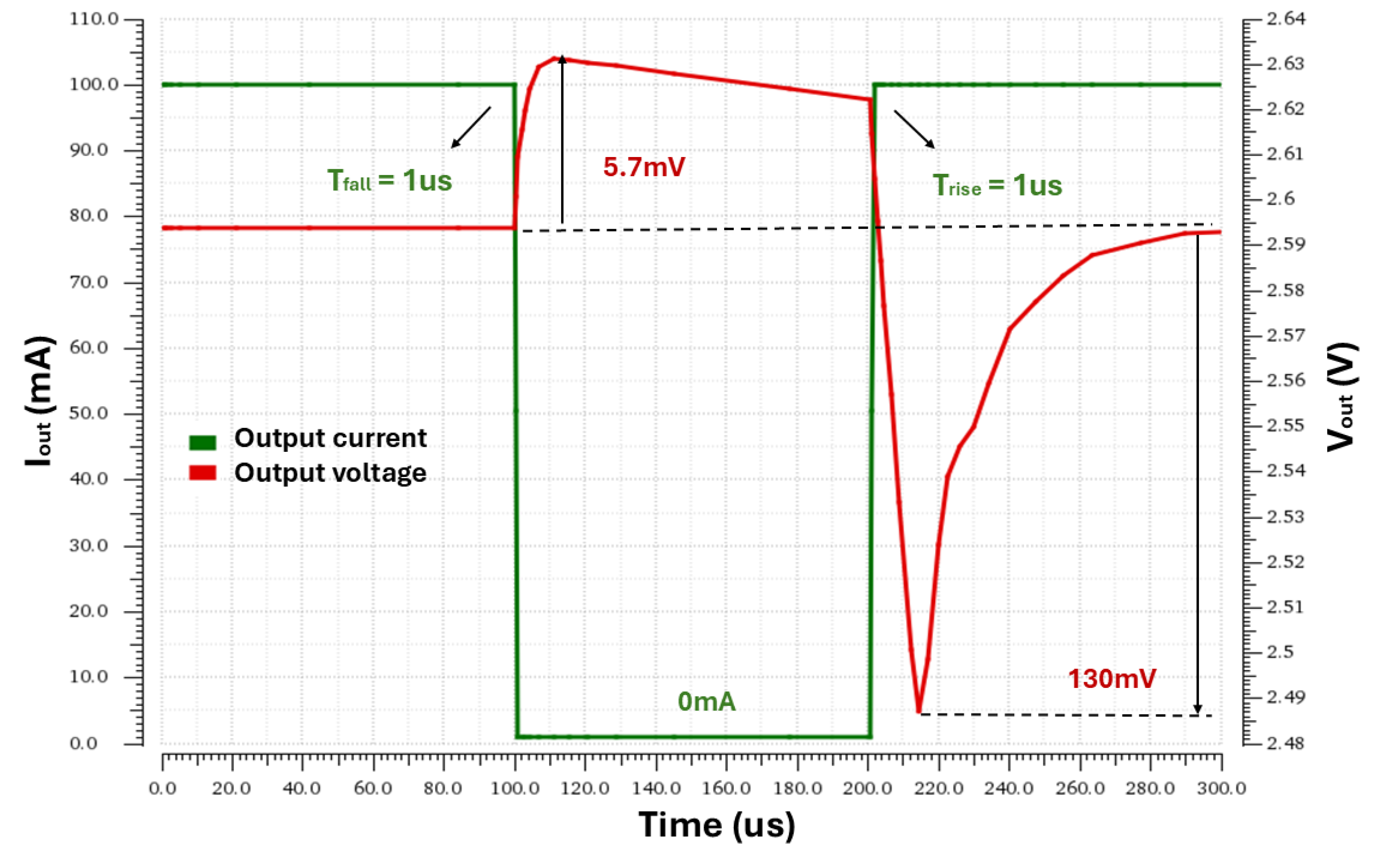
A good transient response is needed in battery-powered applications to ensure that the output regulates with any rapid changes in load current. This could lead to undershoots or overshoots.
Figure 8 illustrates the transient response of LDO, showing that a quick transition in current load from 0 mA to 100 mA happens within a fall time of 1
s. As a result, output voltage overshoots to 5.7 mV and undershoots to 130 mV. The simulation is performed with and without an output capacitor with an Equivalent Series Resistor (ESR) having a value f 10 mΩ.
This is an improvement over the 110 mV undershoot while consuming 10.3
A quiescent current, reported in [
19] for capacitorless LDOs. The addition of a 1 µF output capacitor further improves the transient response, reducing the settling time to 1 µs as illustrated in
Figure 9.
In
Figure 9, the large undershoot is due to the presence of ESR. While capacitors are generally beneficial for transient response by providing transient current, the high ESR has an effect on performance.
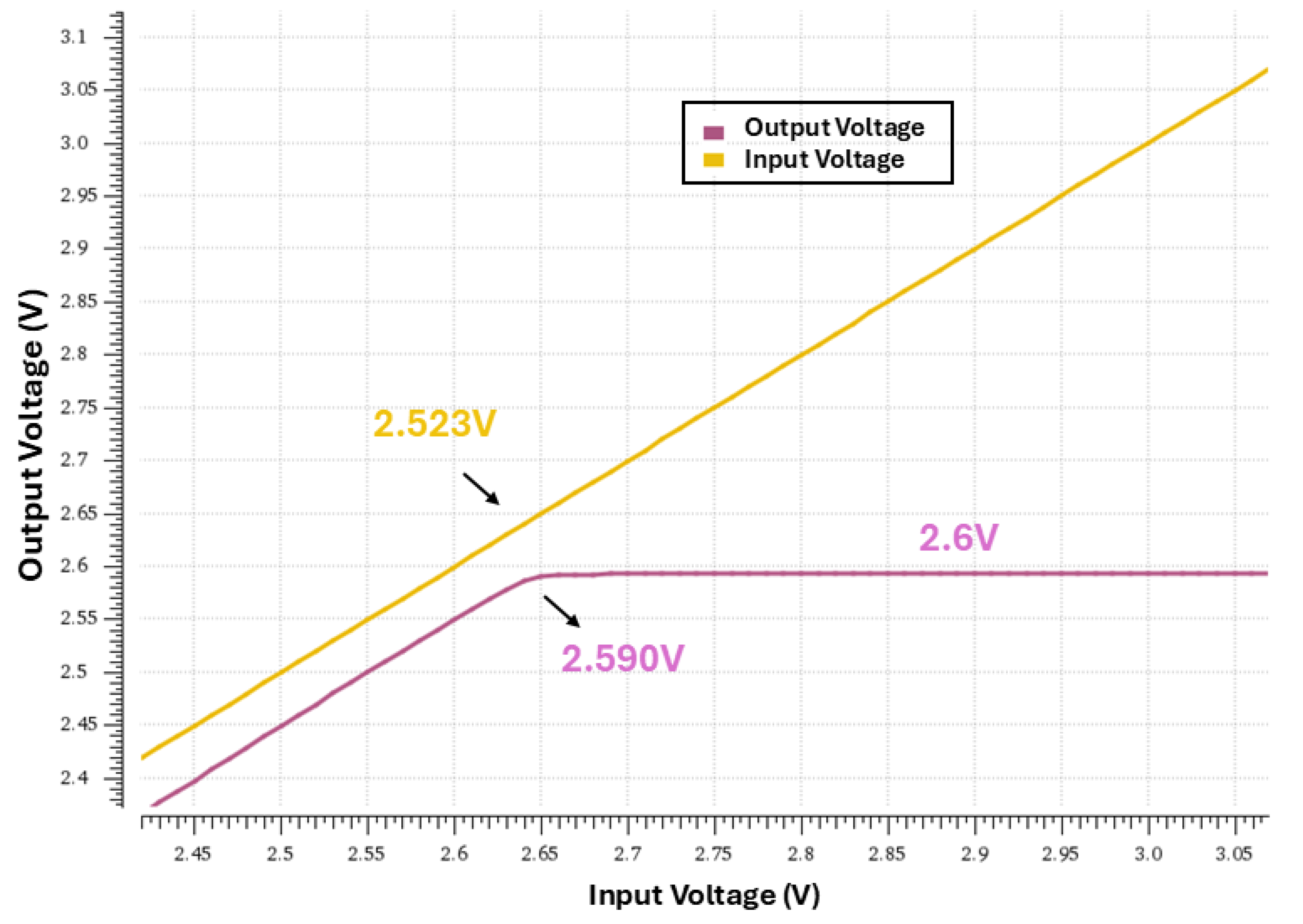
4.4. Dropout Voltage
The behavior of the pass element can be divided into three regions with respect to the input voltage, which are as follows [
20].
In
Figure 10, the region left to the cursor indicates the linear region in which the pass element acts as a resistor, and the behavior of the output voltage can be described by the following Equation (
7):
where
is the load current and
is the ON resistance of the pass element. The knee point indicates that the pass element is in the dropout region. The dropout voltage is given as
The region to the right of the cursor indicates the saturation or regulation region in which the output voltage remains constant with respect to the input voltage. In this region, the pass element acts as a current generator [
21].
The dropout voltage regions can be seen in
Figure 10; the figure was created with a load current of 100 mA.
The minimum dropout voltage shown in
Figure 10 is 67 mV.
4.5. Junction Temperature
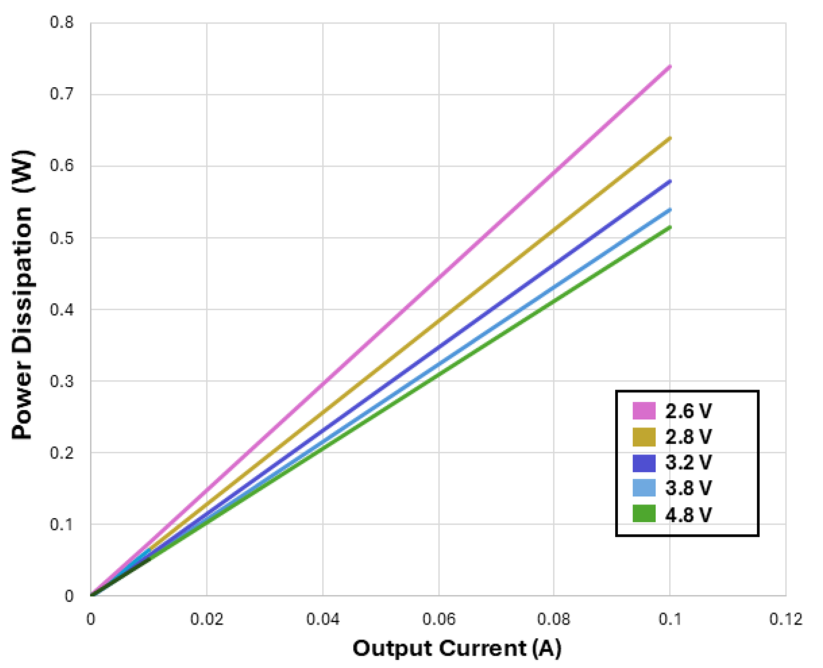
Power dissipation is an important metric in the behavior of LDOs for battery applications. We have calculated the maximum dissipation,
, and the actual dissipation,
, which must be less than or equal to
. The maximum power dissipation limit is determined using the following equation:
where
is the maximum allowable junction temperature;
is the thermal resistance junction to ambient; and
is the ambient temperature.
The power dissipation can be calculated as
where
is the input voltage,
is the output current,
is the output voltage, and
is the quiescent current.
The power dissipation of the proposed LDO is 0.74 W at maximum load current (100 mA) and input voltage (4.8 V), as shown in
Figure 11. This is lower than the 0.8 W reported in [
3] for a similar load current. The low power dissipation, combined with the low quiescent current (5
A), makes the proposed LDO highly efficient for battery-powered applications.
4.6. Static Parameters
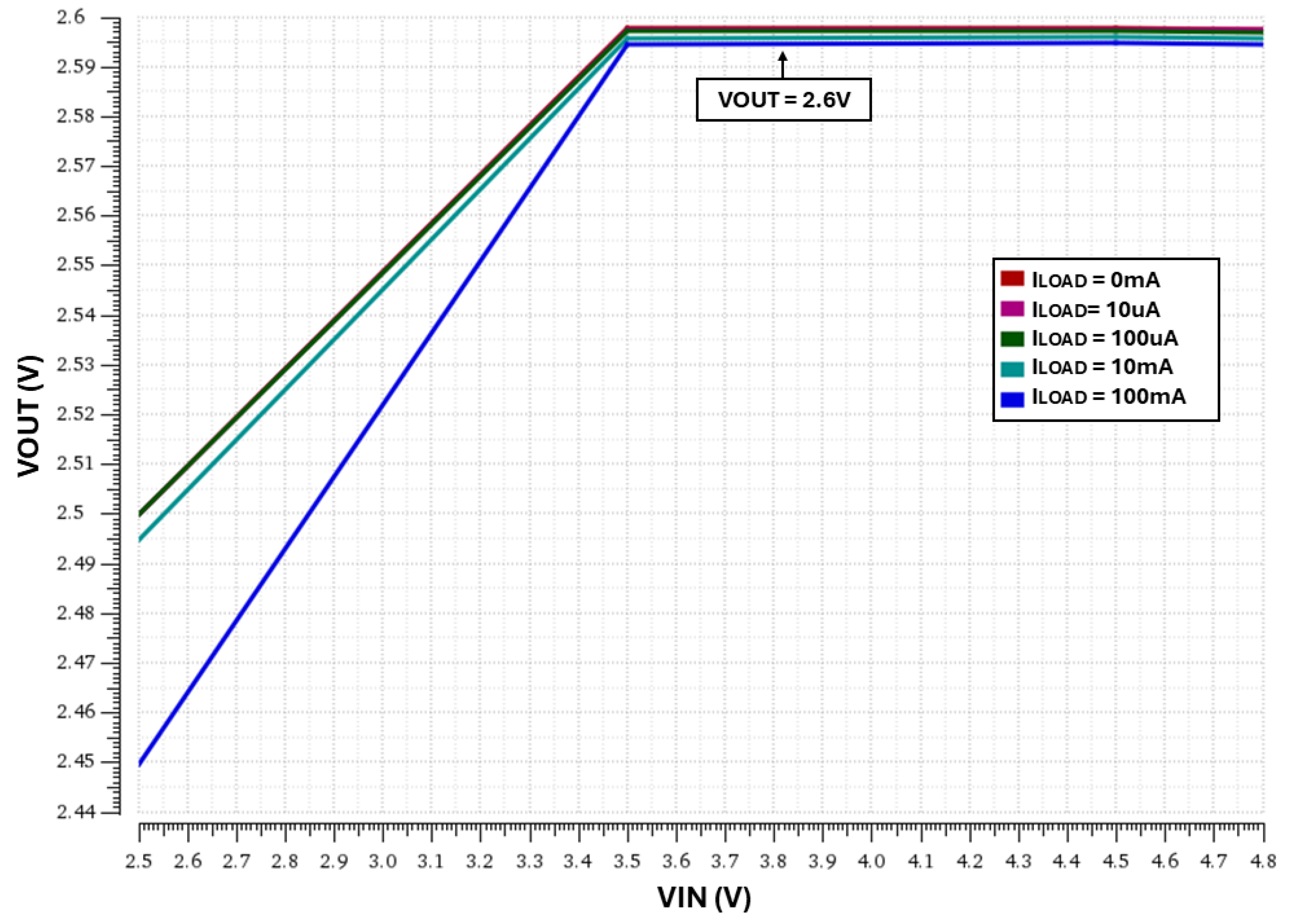
The folded cascode op-amp also ensures the output voltage stability under different load currents due to its high gain.
Figure 12 shows the LDO regulator’s transfer characteristic for different load current values ranging between 0
A and 100 mA. The output voltage exhibits only a slight deviation from the desired value of 2.6 V (by a few
V).
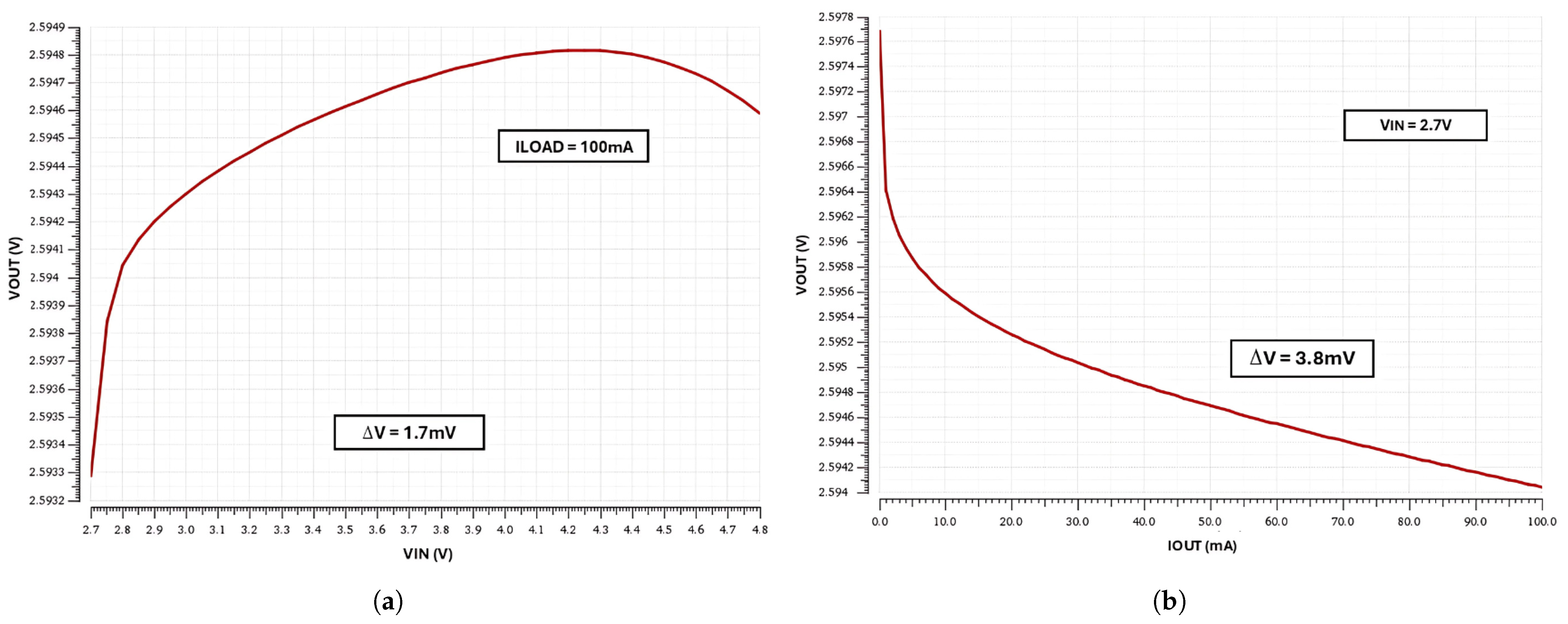
The LDO is simulated to ensure the line and load regulation with changing input voltage and load current, respectively. The line and load regulation are presented in
Figure 13a,b. In
Figure 13a, with maximum load current 100 mA, the input voltage ranges from 2.7 V to 4.8 V, with a minimal change of voltage of 1.7 mV. Hence, the LDO line regulation (LNR) has been calculated as 1.5 mV/2.1 V = 0.71 mV/V.
Similarly,
Figure 13b shows that the load regulation (LDR) with input voltage 2.8 V and load current is increased from 0 mA to 100 mA. The variation in the output voltage is observed as 3.8 mV. Hence, the LDR is calculated as LDR = 3.8 mV/100 mA = 38 mV/A.
Since the error amplifier has a high gain, both the LNR and LDR indicate good performance.
4.7. Corner Analysis
The LDO behavior was simulated under different Process–Voltage–Temperature (PVT) corners, i.e., typical (TYP), Fast–Fast Analysis (FFA), Fast–Slow Analysis (FSA), Slow–Fast Analysis (SFA), and Slow–Slow Analysis (SSA) for input voltage ranging from 2.8 V to 4.8 V (in which the pass element remains in saturation) at three different temperatures: T = −25 °C, T = 27 °C, and T = 125 °C. Maximum and minimum load currents were set, i.e.,
= 0 mA and
= 100 mA.
Table 3 shows the simulated metrics of the LDO regulator under all PVT conditions.
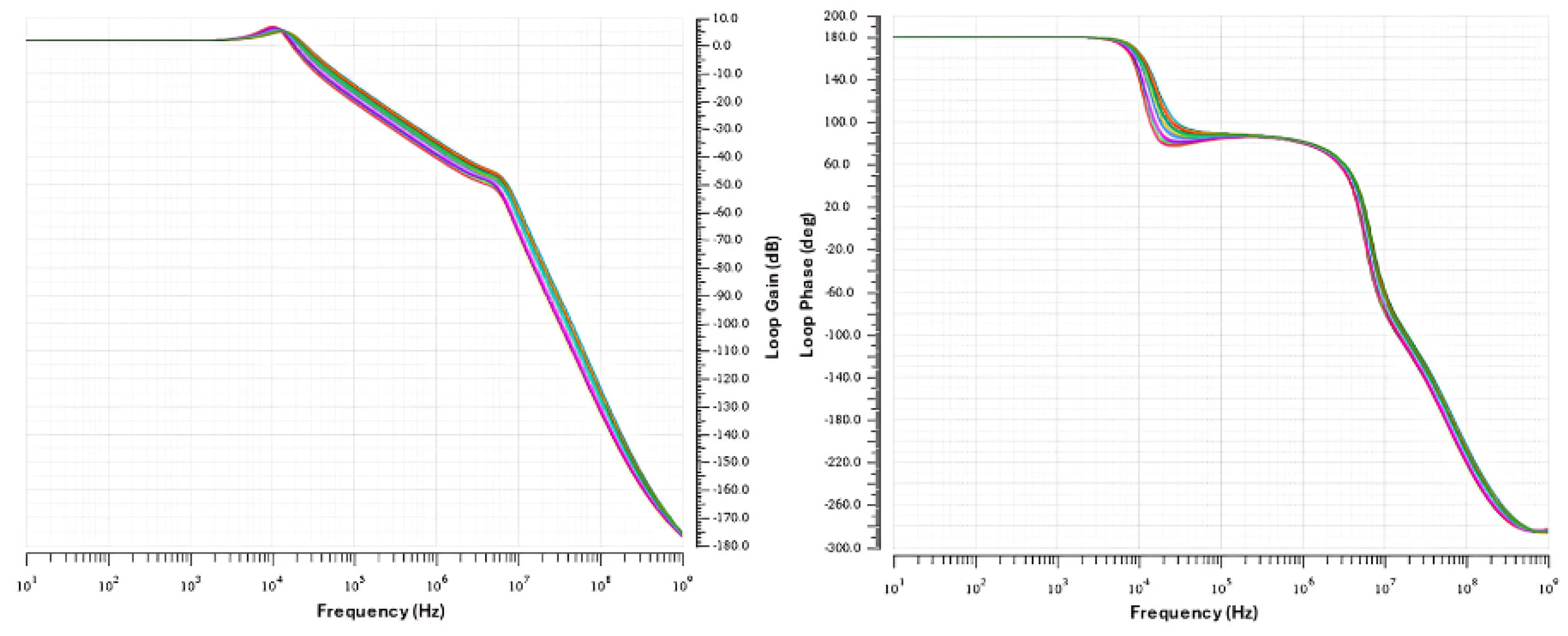
The bode plots of all the corners are presented in
Figure 14. The worst-case
= 2.591 V occurs at the SSA corner at T = +125 °C, for
= 100 mA. The worst-case Phase Margin = 37° occurs at the SSA corner at T = +125 °C at
= 100 mA, while for Quiescent current, the worst case occurs at FFA at T = −25 °C with a value of 5.27
A. For output noise, the max noise = 20
at SSA with T = +125 °C, while the minimum output noise value = 12
at SFA with T = −25 °C.
Figure 15a,b show the line and load regulation curves, for the minimum and maximum values of load current, presenting each process corner. As can be seen, high linearity control is provided in all cases, and a minimum change of 1 mV is provided in the LNR and a minimum change of 5 mV is provided in the observed output voltage.
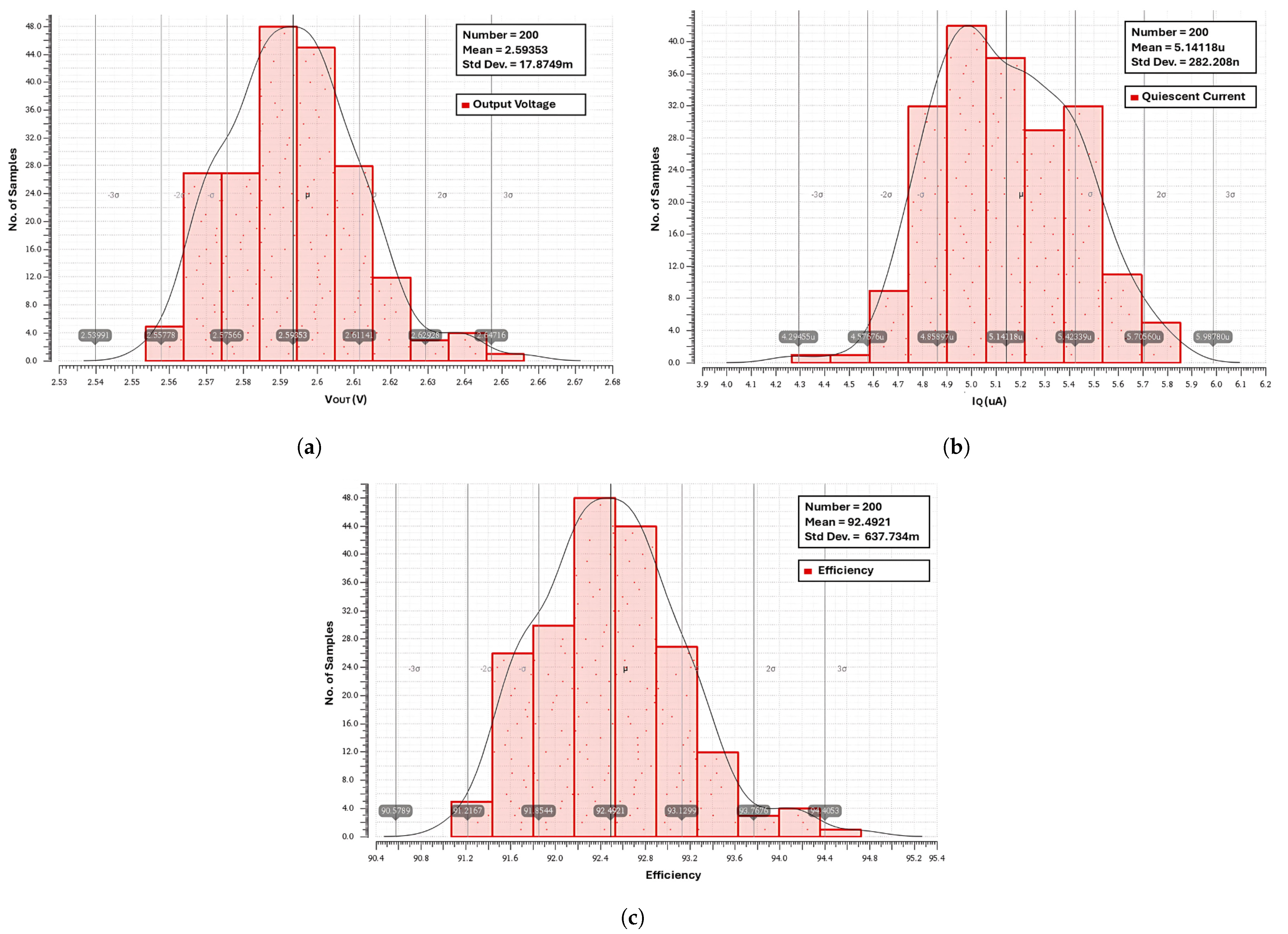
4.8. Monte Carlo Analysis
Monte Carlo analysis was also performed on 200 samples to understand the inconsistencies and process variations. Case scenarios and corner point analysis further improved the design for battery applications. See
Figure 16.
These results show that = 2.595 V, and the maximum value is 2.655 V, which is lower than the worst-case scenario, further reinforcing the necessity of battery usage.
The quiescent current = 5.14 A and the maximum value is 5.85 A, which increases the design to accommodate lower current power consumption.
The optimum efficiency is = 92.5 and the minimum value is = 91.1, indicating good efficiency.
4.9. Figure of Metrics (FOMs)
To quantitatively compare the performance of the proposed LDO with other designs, we use the following Figure of Merit (FOM) from [
18]:
The proposed LDO achieves an FOM of 0.28, which is lower than the 0.45 reported in [
18] and the 0.35 in [
22], indicating superior performance in terms of noise, power efficiency, and transient response.
Table 4 presents a comparison of improved results obtained in this paper in contrast to the previous work carried out. The relevant papers cover a period of about ten years, and the most recent one dates back to 2023; this shows that interest in the topic has always been strong. The proposed LDO achieves a noise level of 14
at 1 kHz, significantly lower than the 22
reported in [
18] and comparable to the 12
in [
22]. Using a folded cascode op-amp with a class AB buffer contributes to this improvement by reducing flicker noise and enhancing stability. Moreover, the dropout voltage of 67 mV is lower than the 200 mV reported in [
3], making the proposed LDO more suitable for low-power applications. However, the design requires a larger output capacitor (1
F) compared to capacitorless designs, which may increase the area overhead.
The proposed LDO introduces several novel features, including the use of a folded cascode op-amp with a class AB buffer for low noise and high stability. The source follower buffer shifts the second pole to a higher frequency, enhancing stability. Additionally, the integrated current limiter protection circuit reduces reverse current from 1.44 A to 763 nA, improving efficiency and reliability in battery-powered applications.
Compared to conventional LDOs, the proposed design achieves a lower noise level (14 ) and a higher gain-bandwidth product (17 kHz), making it suitable for low-power, high-performance applications.
In
Table 4, refs. [
3,
4] represent the simulated results, while the results presented in [
18,
22] are measured.
5. Conclusions
A fully integrated LDO regulator created with a 150 nm CMOS process node is presented in this manuscript. This LDO regulator design maintains a steady 2.6 V output voltage across a wide input voltage span of 2.8 V to 4.8 V and can accommodate load currents ranging from 0 mA to 100 mA, improving its versatility across various operating conditions. With a remarkably low quiescent current of just 5 A, this device demonstrates high efficiency and suitability for SoC applications. The analysis of the LDO across various PVT corners guarantees consistent performance in all operating conditions, enhancing its compatibility with battery applications. The LDO regulator’s static performance highlights exceptional precision, featuring an LNR of 0.71 mV/V, LDR of 38 mV/A, and a low-dropout voltage of = 67 mV, guaranteeing high accuracy across the operational range. Moreover, the transient response reveals notable improvements, including reduced undershoot at 130 mV, limited overshoot at 5.7 mV, and faster settling times, ensuring enhanced stability amid dynamic load changes. Additionally, the design includes a current-limiting protection topology that effectively reduces reverse current from 1.44 A to 763 nA during fast switching, while maintaining simplicity and demonstrating less power consumption, to protect the system from reverse currents and the effects of power loss.
In conclusion, the proposed LDO offers several advantages, including low noise (14 ), low-dropout voltage (67 mV), and high stability (phase margin > 37° under all conditions). Although the design requires a larger output capacitor (1 µF) compared to capacitorless designs, which may increase the area overhead, the proposed LDO is well suited for battery-powered applications due to its low-quiescent-current (5 µA) robust performance across a wide temperature range.


