Article

Through-Hole Buck Converters for Fast Prototyping: A Comparative Study

by
Jose Vicente Muñoz
*,
Luis M. Nieto-Nieto
,
Luis Pulido-Lopez
,
Juan D. Aguilar-Peña
and
Angel Gaspar Gonzalez-Rodriguez
Engineering Department of Electronic and Automation, Higher Polytechnic Engineering School, University of Jaen, Campus de Las Lagunillas, s/n., 23071 Jaen, Spain
*
Author to whom correspondence should be addressed.
Electronics 2025, 14(7), 1273; https://doi.org/10.3390/electronics14071273
Submission received: 2 February 2025 / Revised: 10 March 2025 / Accepted: 13 March 2025 / Published: 24 March 2025
(This article belongs to the Special Issue Power Electronics and Its Applications in Power System)

Abstract

:
The increasing demand for emerging applications like IoT or drones has boosted the interest of industry and academia in DC-DC converters. Due to their high performance, non-isolated buck DC-DC converters have become one of the most common configurations for covering the power demand of portable devices. The current trend focuses on manufacturing these integrated circuits (IC) using surface-mount technology packaging. However, this technology presents disadvantages compared to through-hole devices in pursuing a quick functional circuit. This work aims to guide designers in choosing the most suitable integrated THT buck converter to develop a fast prototype. A comparative market analysis was conducted considering five integrated chip manufacturers to identify the most adequate ICs for this purpose. Then, a comparative experimental study focused on the buck converter LM2576-ADJ by Texas Instruments was carried out. The analysis aims to determine the performance of this IC mounted in a breadboard and stripboard compared to a demonstration board based on SMT technology provided by the manufacturer. Despite their shortcomings, these quick implementations performed remarkably well regarding, among others, line regulation and load regulation (0.37% and –0.33%, respectively), as well as efficiency (up to 79.9%), which indicates that their electrical response was not compromised.

1. Introduction

Power conversion technologies have become increasingly critical across industries, and DC-DC converters are pivotal in enabling efficient energy management. A recent study indicates that the global market for these devices generated $8.76 billion in 2019, and this figure is expected to rise to $17.85 billion in 2027, with an annual growth rate of 11.1% [1]. This growth is driven by emerging applications, such as the Internet of Things (IoT) [2], solar energy harvesting systems [3], and unmanned aerial vehicles [4,5], among others [6,7]. For these applications, which are often battery-powered, non-isolated step-down DC-DC converters are widely used, ensuring reliable power systems while meeting the demands for compactness and efficiency [8,9]. These trends underscore the expanding role of DC-DC converters in advancing sustainable and high-performance technologies.
Non-isolated buck DC-DC converters (Figure 1) have proven to be one of the most efficient ways to cover the power demands of these portable applications (typically up to 15 W) [10,11]. Manufacturers offer integrated DC-DC converters, which integrate in the same package switch and control block, significantly reducing the complexity of the circuit. The use of these integrated circuits simplifies the design of compact and lightweight systems, which are essential for portable and embedded applications. Current trends focus on manufacturing these integrated circuits using surface-mount technology (SMT) packaging. This approach enables reductions in size and weight while promoting large-scale industrial production [12]. However, SMT devices present disadvantages during product development compared to THT components (through-hole technology) [13]. This is primarily due to the tendency of SMT to be a technology optimized for mass production rather than prototyping.
In the early stages of development, prototyping typically begins with proof-of-concept (PoC) prototypes. These prototypes undergo iterative testing and modifications aimed at refining the design into a functional device. During these phases, SMT components present several challenges compared to THT components, particularly in terms of manufacturing costs and development times. SMT components often need to be mounted on custom-designed PCBs (printed circuit boards), which offer limited flexibility for iteration since any modifications require producing new board versions during prototype refinement. This process demands significant time for design and validation, which consequently delays the development. Moreover, the high initial design costs make any unexpected modification unaffordable for low-volume production.
In addition, inspection and testing often require specialized tools such as pick-and-place machines, reflow or wave soldering equipment, and advanced inspection systems [14]. For certain packages, like BGA or QFN, an X-ray inspection is necessary to ensure quality [15]. These tools require skilled technical personnel and substantial investment [16], making the process economically viable only for large-scale production where unit costs are significantly reduced.
To avoid needing custom PCBs during prototyping, breadboards, perforated boards, or stripboards can be used. If SMT components have to be used, and to ensure compatibility with these boards, SMT-to-DIP adapters must be used. These adapters convert SMT components into a DIP (dual in-line package) format suitable for breadboards. Despite this, the approach compromises the primary advantages of SMT components, such as their compact size and reduced parasitic inductance. Furthermore, pre-mounted SMT components on adapters are rarely available on the market. This means that users must manually solder them, an effort that does not eliminate the challenges associated with using these components for prototyping.
Other prototyping techniques, such as those based on ready-made prototype modules or 3D printing, facilitate a prototype closer to the final product. However, these techniques require editing a layout with specific tools, qualified personnel, and demand additional manufacturing resources, as well as skilled staff and longer development time. In addition, they do not easily facilitate modifications to the design, which may become necessary in light of the results of functional tests.
In contrast, THT components are particularly advantageous for early-stage prototyping as they are easy to handle and integrate into various assembly methods [17]. They allow for manual assembly on breadboards, perforated boards, or stripboards without requiring expensive tools or specialized equipment. This flexibility enables rapid iterations, quick modifications, and straightforward testing, significantly accelerating development. Consequently, THT components are ideal for small-scale projects focused on design validation rather than mass production, providing a cost-effective and efficient solution for PoC prototypes. However, questions arise regarding the limitations of these implementations compared to those using SMT components mounted on a PCB. Additionally, it is relevant to know which features a THT-integrated DC-DC buck converter should have to minimize the side effects of using a breadboard or stripboard. Remarkably, despite the extensive use of THT components and prototyping tools such as breadboards, the literature lacks studies that analyze the trade-offs associated with implementing a buck DC-DC converter using THT components during circuit prototyping. Indeed, even though there are scientific works dealing with prototypes mounted in breadboards, authors treat these mounting elements as a medium to achieve a functional prototype [18,19]. However, the limitations and aftermaths linked to implementing the circuit in breadboards are not covered. On other occasions, papers have been published that are related to laboratory teaching, explaining just basic aspects of the electrical response of the prototype [20,21,22].
Focusing on the buck topology with an integrated chip that integrates the switch and control block (Figure 1), this paper addresses two main objectives. First, it aims to guide rapid prototyping using a THT buck integrated circuit (IC) on a breadboard or stripboard. Thus, a comparative analysis of five leading manufacturers is conducted to identify the most adequate component for this purpose. The selection has been narrowed according to a precise number of features that facilitate fast prototyping and play down the effects of not having the circuit mounted in a PCB. Once the best-integrated buck converters have been identified, the second target of this paper is to provide relevant insights into the limitations of these types of assemblies compared to those implemented on a PCB with SMT components. This information is particularly valuable as, despite the widespread use and low cost of breadboards, there is limited understanding of how their inherent constraints can impact the expected electrical performance of a buck DC-DC converter.
The current study is arranged as follows. Section 2 exposes the most important features that should be considered when selecting a THT-integrated buck converter suitable for fast prototyping. Section 3 is divided into two parts. In Section 3.1, the results extracted from market research carried out among five manufacturers of THT-integrated buck DC-DC converters are given. Secondly, in Section 3.2, one of the most notable THT-integrated buck converters from the previous market study is used to implement two prototypes. Then, a comparative study is conducted, including experimental and simulated results. Features from the two prototypes mounted on a breadboard and a stripboard are compared to its replica mounted in a PCB using SMT components. Finally, the most important conclusions extracted from this work are summarized in Section 4.

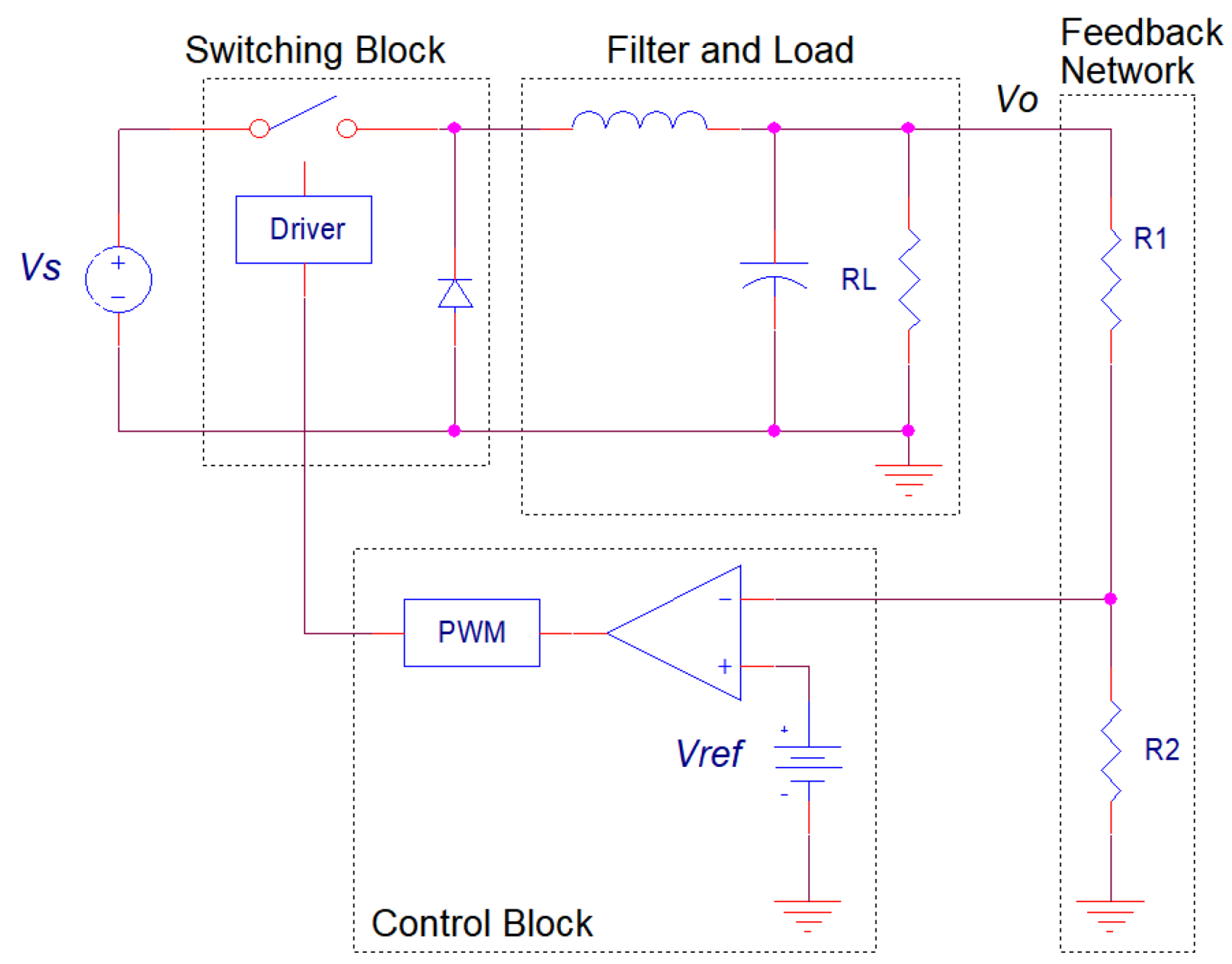
2. Material and Methods

This section defines the most important features that a specific buck-switching regulator should have to meet the requirements for fast design and implementation. These characteristics will drive the selection of the most adequate integrated buck circuit converters on the market for fast prototyping, which is carried out in Section 3.1. The desirable features that must be taken into account have been divided into three categories and are described in the following.

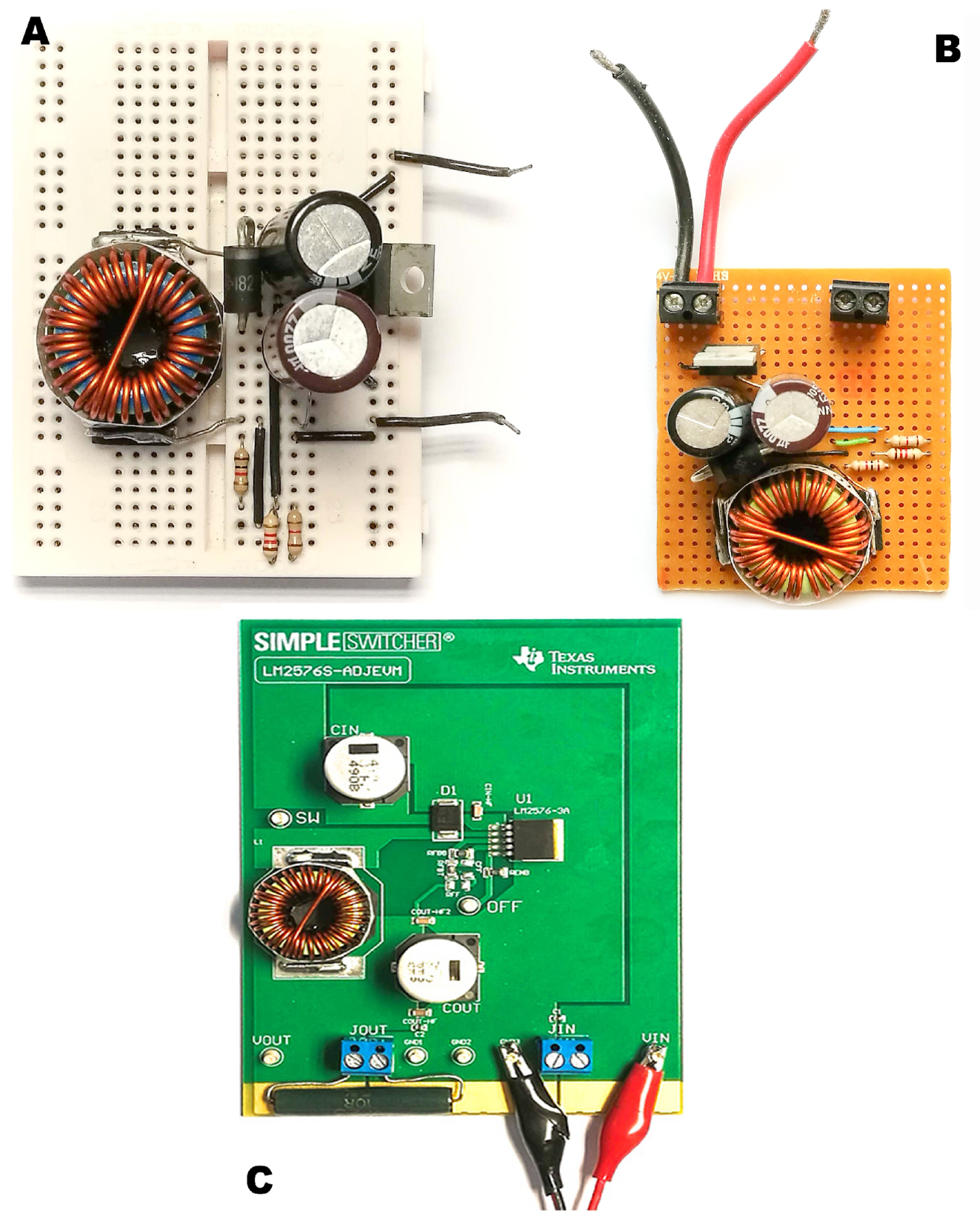
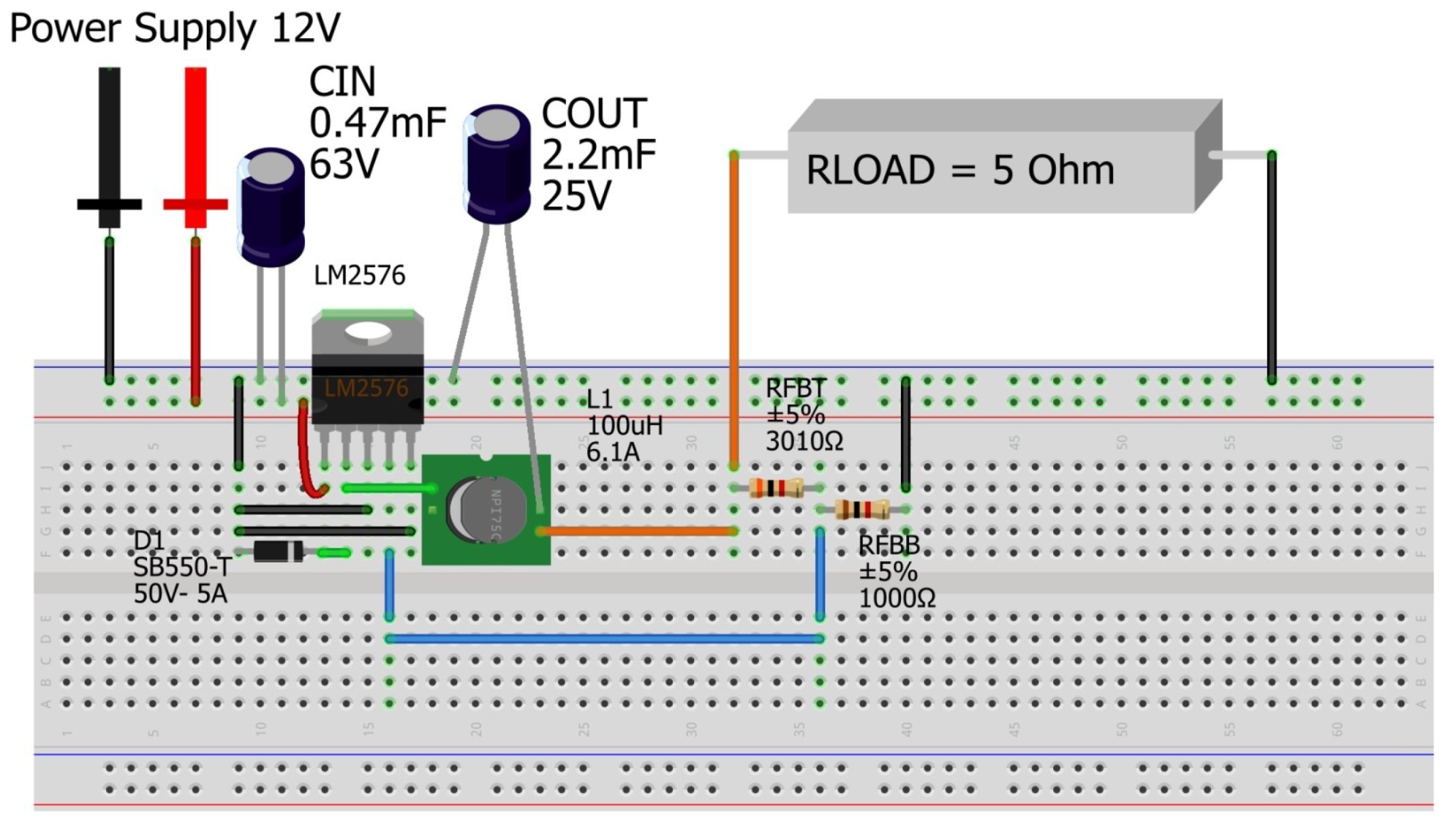
2.1. Design and Customization

Designers have to count on tools that make the process of designing the DC-DC buck converter a non-time-consuming task. Focused on the use of an integrated circuit, such as the one shown in Figure 2 (control and switching blocks gathered in a single IC) working in continuous mode, the design encompasses the computation and selection of at least six surrounding components: fast recovery diode, coil, input and output capacitor, and two resistors for the feedback network. It is worthwhile to mention that depending on the integrated circuit, a compensation network consisting of a resistor and capacitor may also be also needed. In this sense, some manufacturers have greatly streamlined the design procedure of buck converters via integrated solutions, which alleviate the need for theoretical computations. IC firms include many application notes, full examples of designs, and handy tables to support the technical design process. The documentation generally specifies commercial devices from relevant brands in the market for coils, capacitors, or diodes. As commented later, the logistics related to the components’ availability is a pivotal matter for fast prototyping and must be considered thoughtfully. Finally, it is also useful to utilize online design tools to help choose the most appropriate electronic component depending on the application [23,24]. In other cases, the availability of the Spice model of the buck converter is a significant help for designers, which tips the scale in favor of one IC or another.

2.2. Technical Issues to Overcome

Technical issues during the prototyping of a buck DC-DC converter are tightly connected to the available equipment in the laboratory. As a reference, standard equipment can be considered to be the common instrumentation available in a higher education laboratory. In this sense, a multimeter, a two-channel oscilloscope, a signal generator, and a two-channel power supply are part of the standard set available in these places. Finally, the breadboard is used to make connections by inserting through-hole components. The stripboard with components soldered can also be used, especially when there is a high output power demand. Accordingly, the most critical technical issues a designer should consider when choosing the most appropriate buck-integrated switching regulator for their practical sessions are listed below.

2.2.1. Frequency and Current

The breadboard and stripboard present limitations regarding the level of current and frequency which they can deal with. Owing to its connection system, there are inductive and capacitive parasitic impedances which limit the maximum operation frequency of a breadboard up to, typically, 10 MHz [25,26]. That represents again a setback because there is a clear tendency to increase the switching frequency of buck DC-DC converters in order to minimize the size of the coil [12,27,28]. Consequently, switching frequency must be carefully taken into consideration when choosing a buck converter.
Apart from the limit of 10 MHz imposed by the breadboard, the laboratory oscilloscope’s bandwidth must be thoroughly revised. An oscilloscope is required to measure the output ripple and to verify that the current through the inductor ( i L ( t ) ) does not cancel (continuous mode). For a suitable visualisation of the squared signal, at least the 10th harmonic should be captured by the laboratory oscilloscope, whose bandwidth is around 10 MHz. Consequently, the maximum switching frequency of the buck converter under test has to be 1 MHz.
Concerning the output current, the breadboard internal bars usually limit it to 1 A [25]. This is not a major issue since the converter will not work in a laboratory under high current demand for an extended period. Indeed, the limitation can be dodged as long as the user makes the device work for a period that is short enough to hold the response on the oscilloscope right after switching the input source off. However, for extended periods of operation, commercially available stripboards with 1 oz/ft² copper and 1.6 mm track width can be employed [29]. These types of boards can handle currents exceeding 3 A while maintaining a temperature rise below 10 °C, ensuring reliable long-term operation.

2.2.2. Compactness

The compactness of the design can be boosted as long as an integrated switching regulator that includes switching and control blocks on the same chip is selected. These devices are a better option than other buck converters where switching and control blocks are independently mounted. This integrated solution not only makes the theoretical design process easier but also simplifies the mounting process due to the reduced number of necessary elements. Another advantage of using an integrated circuit is the consequent reduction in the current loop area as long as layout recommendations—which will be commented on in detail below—are followed. This will constrain electromagnetic interference (EMI), which is beneficial in obtaining better results in the laboratory.

2.2.3. Layout Recommendations

As is remarked by integrated buck converter manufacturers, the circuit layout is critical for its proper operation [30,31,32,33]. The most important recommendation is to keep the AC loops as small as possible in order to minimize the effect of switching noise generated by the switching block. Indeed, according to the manufacturer, the length of the leads, indicated by heavy lines in Figure 2, should be kept as short as possible to minimize this issue. These loops include the Schottky diode and the inductance, which should be placed close to the integrated buck converter (Figure 2). In addition, the length of the cables and their height over the breadboard should be reduced, while also considering that crossovers among wires must be avoided to prevent EMI coupling [34,35,36]. Another EMI-sensitive connection is the feedback network line implemented by the voltage divider. Although it is not a high current line, its loop area should also be minimized, and any crossing with other power lines should be avoided to prevent picking up EMI noise generated by the circuit itself. Finally, special attention should be paid to the wire gauge chosen to carry out the interconnections among components in the breadboard or stripboard. A proper wire gauge and length are essential to provide good connections and reduce the parasitic inductance in switched power lines, which causes high-frequency noise.

2.2.4. Manufacturer Demonstration Board

Some manufacturers provide demonstration PCB boards with all the components of the buck DC-DC converter already soldered. This is a handy aid for designers. Indeed, the demonstration board enables the designed to quickly obtain electric responses to compare with the ones obtained on a breadboard. The demonstration board can also be used to compare the ideal response of the circuit with the one mounted on a breadboard or stripboard. As is analyzed in Section 3.2, this comparison provides valuable information that allows designers to understand the limitations of the implemented prototype.

2.3. Logistic and Economic Aspects to Consider

The cost and availability of the elements used in the practical session play a paramount role when a prototype has to be designed and implemented. Firstly, the electronic components of the buck circuit must be affordable, especially at this stage of circuit development, due to the high risk of misconnections and, consequently, damaged devices. If components of a DC-DC converter with an integrated switching regulator are considered (Figure 2), the most expensive elements are the integrated circuit and the coil. The features of the coil make it difficult to damage destroy during the implementation. As a result, the price of the integrated switching regulator is the key to remaining on budget.
Private institutions have access to a wide range of distribution channels without restriction. However, public higher education centres and governmental research institutions have a limited number of distributors which accept their policies. These companies can vary depending on the country and the governmental rules. However, due to its easy accessibility for private and public institutions, the following international electronic distributors have been considered: RS Amidata, Mouser, Farnell, and Digi-Key (in this order).

3. Results

Firstly, a comparison of the most suitable non-isolated DC-DC buck converters on the market to build a fast prototype was performed. The features highlighted in Section 2 were considered to assess the most suitable buck-integrated circuit for this purpose.

3.1. Integrated Buck Switching Regulators on the Market: A Comparison

As per the claims stated in Section 2, the comparison to find the adequate buck switching regulator on the market was narrowed to those which include switching and control blocks in the same chip (Figure 1). In addition, every integrated buck regulator included in the following comparison must allow through-hole mounting.
Thus, Table 1 summarizes the most relevant buck regulators on the market and their features. The manufacturer and model are shown, respectively, in columns 1 and 2. The availability of the devices listed in the table has been checked according to their stock on 5th of February 2024 on the Spanish websites of the four distributors mentioned above of electronic components: RS Amidata, Mouser, Farnell, and Digi-Key (13th column in Table 1, represented by 1, 2, 3 and 4, respectively). Unless otherwise indicated, the unitary price shown in this Table corresponds to the costs given on the RS Amidata webpage.
The 3rd and 4th columns summarize the electric input/output characteristics, respectively. In many cases, the difference between these characteristics gives an idea of the internal drop-voltage [37,38].
The 5th column indicates the maximum output current of the device, which has a concordance to the package of the integrated circuit (6th column). Devices that provide high currents usually exhibit packages that accept a heat sink, although that would require extra components, tools, and time for its mounting. For the TO-220 packages with up to five pins, it is advisable to order the 314D variant, which comes with all of the pins in line.
The 7th column defines the voltage output of the buck converter, and this feature can be fixed or adjustable depending on the device. Fixed versions monolithically include the feedback network of the DC-DC converter. On the other hand, in adjustable models, the feedback network is external and can be designed for a specific voltage or a range of voltages.
The switching frequency shown in the 8th column is one of the essential features in this study, and its value is critical so as not to have setbacks in the laboratory—the breadboard limits the switching frequency to 200 kHz. As seen in this column, none of the models work beyond this value.
The 9th column represents the availability of a demonstration board marketed by the manufacturer. This is important because it gives the instructor a functional and compact example of the buck DC-DC converter. Unfortunately, only two manufacturers, Texas Instrument and Maxim Integrated (San Jose, CA, USA), provided this helpful resource, though not for all their models.
Column 10 refers to the components needed to make the buck converter work. Most require six for fixed switching regulators and eight for adjustable ones (Figure 2). Such numbers include the integrated buck converter and a load resistor to test the performance of the power supply unit.
An orientating unitary price (based on the cost on the RS Amidata webpage) is shown in the 11th column in Table 1. Most ICs have a price lower than EUR 5, except for Analog Devices (Wilmington, MA, USA) and ST Microelectronic (Plan-les-Ouates, Switzerland), which include extra features such as output current limiters or battery controls.
Column 12 refers to the availability of the Spice model for the IC. For this comparative study, OrCADTM PSpiceTM V.17.2 by Cadence (San Jose, CA, USA) has been selected due to its traditional popularity. The following symbols are used: (i) when the Spice model appears by default in the OrCAD library database of components; (ii) when the Spice model is available to be downloaded on the manufacturer’s website; (iii) if the companies provide an online simulation tool (such as WebenchTM by Texas Instruments (Dallas, TX, USA)) or a particular free software (like LTSpiceTM V.24 or LTPowerCADTM II V.2.0 by Analog Devices). According to the results, buck converters manufactured by Texas Instruments and Analog Devices provide better ease of simulation.

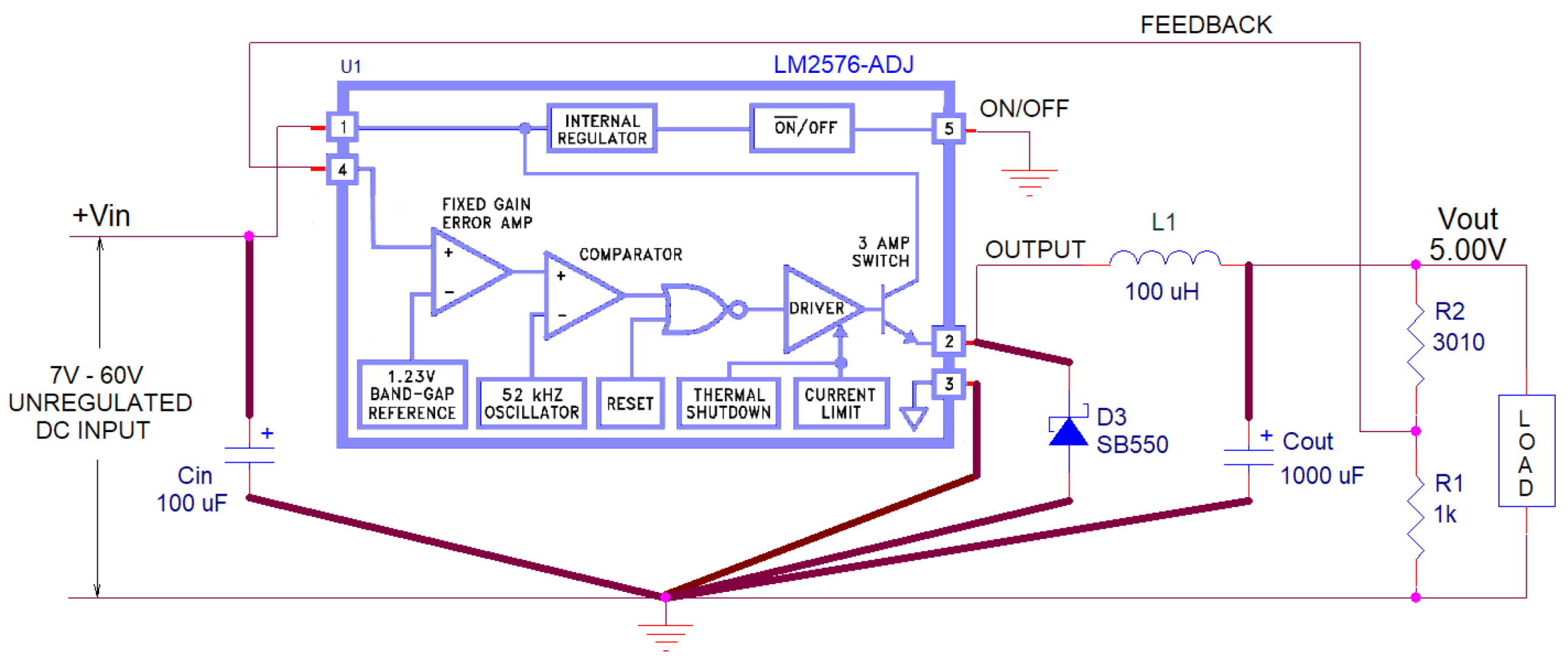
Candidate from the Comparison: LM2576-ADJ by Texas Instruments

Many of the integrated circuits included in Table 1 are excellent candidates for the design and implementation of a quick THT DC-DC buck converter prototype. Nevertheless, one model has features that make it ideal for designers and ideal for this task due to the following advantages:
  • Its output current is remarkable (3 A), particularly when it comes in a manageable TO-220 package, which allows a heat sink to be easily installed.
  • The wide input/output voltage range, as well as the possibility of using the fixed or adjustable version (7th column in Table 1), make this buck converter ideal from a practical point of view.
  • Another distinguishing mark of the LM2576-ADJ is the ease with which it can be designed, simulated, or tested. The electronic component by Texas Instruments comes with an excellent datasheet with examples and tools to simplify the design process. The buck converter can be simulated online thanks to the WebenchTM tool, and its Spice model is also available in the list of components on the OrCADTM PSpiceTM 17.2 database. Moreover, the manufacturer offers a demonstration board, which is always helpful for designers.
  • Its price and availability are also points in favor of the LM2576-ADJ. It is one of the cheapest switching regulators included in the study and is marketed by all the distributors that have been taken into account. Moreover, this buck converter is sold by two electronic firms, Texas Instruments and ON Semiconductor Corporation (Scottsdale, AZ, USA), which is also an advantage because its availability is more likely.

3.2. Experimental Comparison Focused on the LM2576-ADJ

The following paragraphs describe the experimental study conducted by implementing two DC-DC buck prototypes based on the LM2576-ADJ. This integrated circuit, shown in Figure 2, incorporates both the switch and the control block within a single package. Such integration simplifies the design process by reducing the number of external components required while also ensuring stable operation with a wide input voltage range (4 V to 40 V) and an adjustable output voltage (1.23 V to 37 V).
The prototypes were implemented on a breadboard (Figure 3A) and a stripboard (Figure 3B), and compared against a demonstration board designed and manufactured by Texas Instruments. This board features SMT components mounted on a PCB, and is considered the benchmark for optimal physical implementation (Figure 3C). The objective of this study was to evaluate the degree of agreement between the performance of the breadboard implementation and that of the two soldered implementations. To ensure consistency, all three implementations utilized the same electronic components, aiming to replicate the performance of the demonstration board as closely as possible.
These components are listed in the Texas Instruments LM2576S-ADJEVM User’s Guide [39]. However, it is worthwhile to mention that the demonstration board includes particular electronic components—for example, decoupling capacitors—to minimize the noise at the output [35,36,40], which, although they are recommended, are not essential. Focused on the aim of having a quick prototype, only essential components ( C i n , C o u t , D, L, feedback network, and LM2576-ADJ) were included in the breadboard and stripboard implementations (Figure 4). Furthermore, the SMT components from the demonstration board were replaced by their twin components using through-hole technology, except for the coil. Wire terminals were soldered for this component to connect it to the breadboard. To improve the reproducibility of the results commented below, Table 2 gathers the manufacturer reference for the electronic components which were connected with the IC LM2576-ADJ (Figure 4).
Finally, software simulations of the circuit using OrCADTM PSpiceTM V.17.2 were also analyzed and compared to the physical implementations. Accordingly, the simulation results represent the theoretical response of the buck converter.

3.3. Comparison of the Implementations

The comparison of the three implementations encompasses the analysis of their electrical response in the laboratory as well as simulations. It is worthwhile to mention that the central aim of this comparison is to understand which malfunctions or deviations in the electrical response of the circuit can be attached to the use of platforms ideal for fast prototyping, like breadboards or stripboards. Thus, since the breadboard and stripboard circuits were replicas of the demonstration one, they theoretically share the same features, which mainly include 5 V of output voltage, 3 A of maximum output current, and an input voltage ranging between 7 V and 40 V. The performance of the three DC-DC converters was evaluated by measuring the following parameters: output voltage ripple, line regulation, load regulation, coil current ripple, duty cycle evolution under different loads, efficiency, and thermal response. The obtained results are explained in the following.

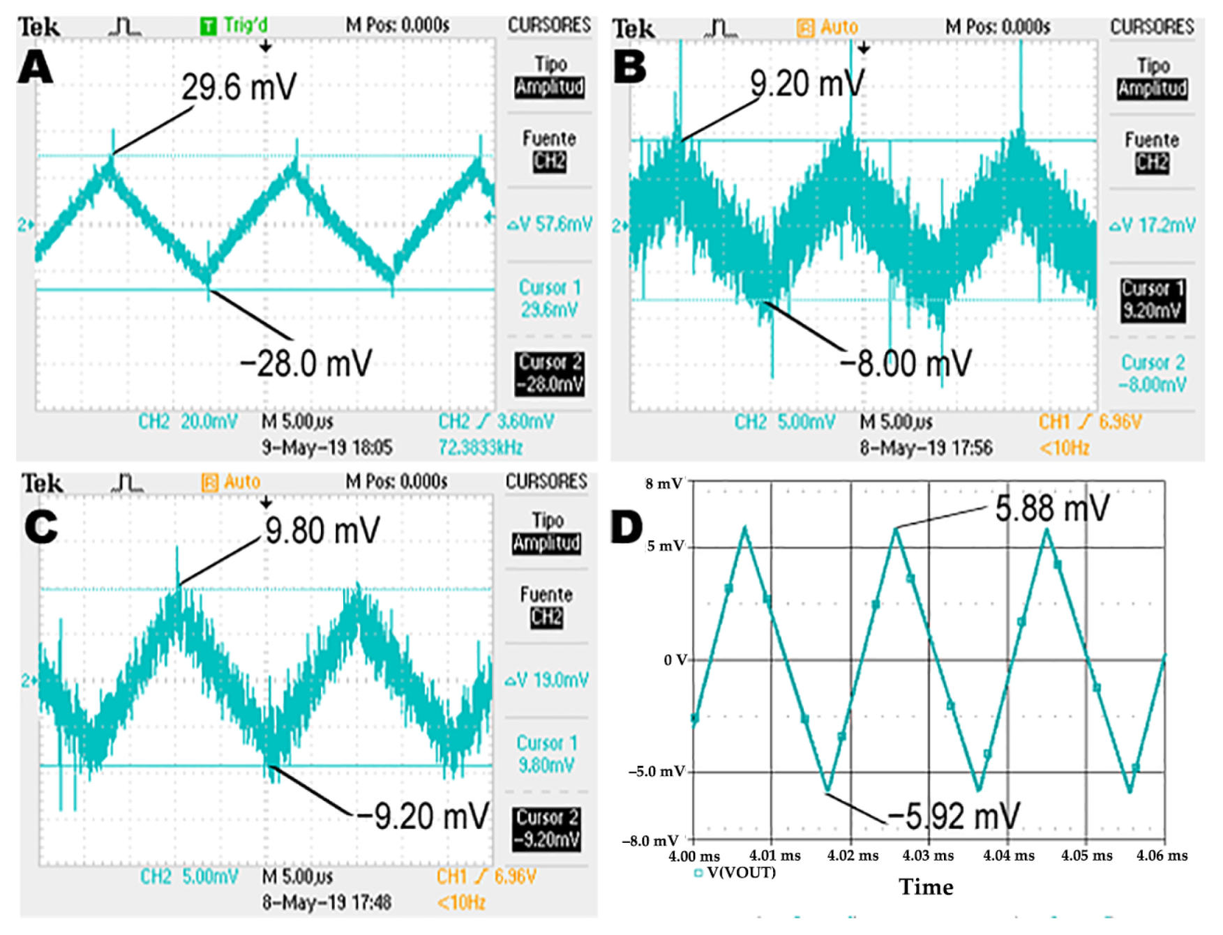
3.3.1. Output Voltage Ripple

The quality of a voltage regulator is tightly linked to the voltage ripple at the output. The ripple can increase due to imperfections in the circuit’s and components’ physical implementation (ESR of output capacitors, parasite capacitors, unexpected defective contacts, etc.). For this experiment, the circuit shown in Figure 2 was implemented, and a load resistor equal to 5.04 Ω (all resistors included in the study were measured under four-wire configuration) was set. A DC input voltage of 12 V from a DC power supply was connected at the input. Figure 5 shows the decoupled output voltage obtained for the breadboard (A), stripboard (B), demonstration board (C), and software simulation (D). The second column of Table 3 summarizes the numerical results related to the output voltage ripple. As can be deduced from the results, the maximum ripple for the simulated circuit was 11.8 m V p k p k , which represents the ideal response. At the same time, the demonstration board, stripboard, and breadboard achieved 19.0 m V p k p k , 17.2 m V p k p k , and 57.6 m V p k p k , respectively.
As expected, the breadboard configuration achieved the highest output voltage ripple due to more physical imperfections. What is more, configurations mounted and soldered reached output ripple voltages close to those obtained by simulation. Although the voltage ripple for the breadboard was almost three times higher than the solder implementations, it is still a correct result according to the manufacturer’s datasheet. Texas Instruments claims that an acceptable ripple voltage is approximately 1% of the output, understood for a soldered circuit. Thus, the resulting value of 57.6 m V p k p k for a breadboard with all its imperfections is a permissible value. All in all, this larger voltage ripple can be significantly reduced if an output capacitor with less equivalent series resistance is used.

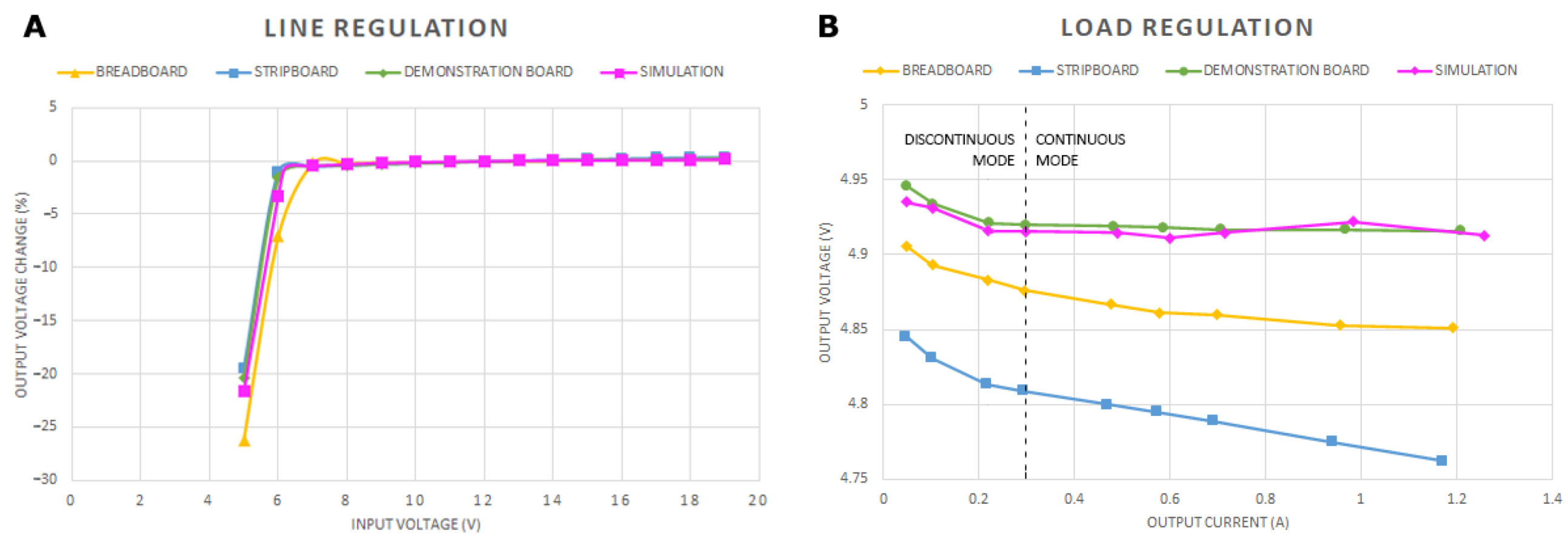
3.3.2. Line Regulation

The line regulation is the ability of the DC-DC converter to maintain a constant output voltage (5 V for the whole study) despite changes to the input voltage, keeping the output current constant (5.04 Ω resistant as a constant load). It is defined as follows when the output current is constant:
R e g l i n e = Δ V o Δ V i
where V o , I o , and V i are the output voltage, output current, and input voltage, respectively, and Δ refers to their increments when V i changes. Thus, the input voltage was connected to the DC laboratory power supply and was modified from 5 V to 19 V for the three configurations. It is worth mentioning that according to the manufacturer’s datasheet, the LM2576-ADJ input voltage range is constrained between 40 V and a value close to 2 V above the output voltage. Since the three configurations were adjusted to deliver 5 V at the output, 7 V is the minimum acceptable voltage at the input. However, it is interesting to know the lowest input voltage limit at which the LM2576-ADJ can work as expected. This is the reason why the experiment was conducted from an initial input voltage of 5 V rather than 7 V.
Figure 6A graphically shows the experimental results from the line regulation test. The tendency followed by the four configurations is very similar and can be divided into two sections. As long as the voltage drops below a breaking point close to 7 V, all the configurations perform poorly: small changes at the input are translated into significant changes at the output. Once the input voltage stays above this limit, all the configurations work significantly better, and the output voltage remains regulated regardless of the input voltage. For this reason, the numerical values of the line regulation (Table 3) have been computed considering a variation in the input voltage ranging from 8 V to 19 V. Under this consideration, if the breadboard implementation is considered, the output voltage varies by just 0.37%. It should be said that the aforementioned breaking point is not reached for all the configurations at the same input voltage. Those configurations with their components soldered performed very similarly to the simulation results. They entered into the regulated region for an input voltage close to 6.4 V, which represents 1.4 V above the output voltage (5 V). The last configuration to achieve the regulated region was the breadboard-based one. For this configuration, an input voltage of nearly 3 V above that of the output was needed to operate in the regulated area. According to the datasheet, that represents a value worse than expected (2 V above the output voltage should be enough to make the device work properly). The limitations of the breadboard lie behind this setback.

3.3.3. Load Regulation

The load regulation is the ability of the DC-DC converter to maintain a constant output voltage despite changes to the output current, while keeping the input voltage constant. It is defined as follows when the input voltage is constant:
R e g l o a d = V o i = 0 V o V o r a t e d V o i = 0 V o V o i = 0
where V o i = 0 is the no-load output voltage and V o r a t e d is the output voltage at rated output current.
Testing the load regulation requires the output current to be varied and the output voltage to be measured. This experiment was conducted by fixing the input voltage at 12 V, employing the laboratory DC power supply and using a set of load resistors ranging between 101.49 Ω and 4.07 Ω , which translates into output currents between 0.05 A and 1.26 A according to simulated results. The maximum output current for this experiment was limited at 1.21 A, which is higher than the limit breadboard of 1 A recommended, but admissible if the experiment is not delayed.
Figure 6B shows how the output voltage behaves for the three physical configurations and the simulated circuit when the output resistance changes (load regulation). The dashed line points out the limit between continuous and discontinuous modes, which will be discussed later. Due to this analysis being focused on continuous mode, the numerical computation of the load regulation has been narrowed for values of output currents ranged from 0.48 A to 1.21 A. Results for the load regulation constrained to this range are shown in Table 3. Thus, for the demonstration board, the load regulation is 0.06%, almost matching the result obtained by the simulation (0.04%). The breadboard configuration performed an intermediate response with an output voltage variation of 0.33% for the aforementioned output current change. All in all, a variation of 0.33% when the current demand is around 1.2 A can be considered an excellent result for a circuit mounted on a breadboard. The worst response was obtained with the buck converter implemented on a stripboard (blue line). In this case, the voltage dropped 0.79% when the supply of current changed from 0.47 A to 1.17 A. Without further tests, this inadequate response could result from a too-high AC current loop or a faulty solder whose parasite resistance is boosted by the high current level at the output.

3.3.4. Coil Current Ripple

The current ripple through the coil has a pivotal impact on the performance of the buck DC-DC converter. Parameters such as voltage output ripple or the transition between continuous or discontinuous modes are tightly connected to the coil current ripple. Moreover, from a teaching point of view, the transient of the current across the coil is one of the most relevant charts to be captured in the laboratory when a buck converter is under study. When i L ( t ) has to be plotted, the implementation mounted on a breadboard makes sense because it is the only one that allows a shunt resistor to be included to record the current through the inductor. Thus, this section of the experimental study was only conducted by simulation, and the buck converter was mounted in the breadboard.
A calibrated shunt resistance of 0.1 Ω was included in the series with the 100 μ H coil. Then, the scale of the oscilloscope was adjusted (factor 1/10) to have straightforward current readings from voltage ones (Figure 7A). The continuous and discontinuous modes were forced using the appropriate load resistors. According to the manufacturer, the output current demand triggers the continuous or discontinuous mode. The limit of 300 mA sets the boundary between the two regions. Output currents lower than this limit make the converter work in discontinuous mode; conversely, output demand higher than 300 mA forces the continuous mode. Thus, the experiment was carried out first with a load resistor of 10.22 Ω while the input voltage remained constant at 12 V. Plots for i L ( t ) and the duty cycle of the buck converter for breadboard and simulated circuit are included in Figure 7A and Figure 7B, respectively.
The evolution of the current across the inductor for the breadboard configuration has the expected triangular shape but with current peaks at the vertexes due to the noise caused by the regulator’s switching process. Those phenomena are not visible in the simulation. If switching peaks are ignored, the minimum value of i L ( t ) according to Figure 7 was 0.24 A for the simulation and 0.27 A for the experimental test. The amplitude peak to peak of i L ( t ) was also measured, and 0.53 A p k p k and 0.59 A p k p k were obtained for the simulation and the experimental analysis, respectively. This result represents a discrepancy of 11.3%, highlighting an excellent closeness of agreement between both configurations as long as the switching peaks are neglected. Furthermore, the output current—which is equal to the average current across the coil, 0.501 A (Figure 7A)—is higher than the limit that triggers the continuous mode (0.3 A). That is visible in Figure 7 given that i L ( t ) never cancels. That situation causes a regular square shape for the duty cycle, as shown.
One of the most remarkable features of the LM2576-ADJ is its capability to trigger the discontinuous current mode across the coil only with the adequate selection of the load resistor. Figure 8 shows the comparison between the results obtained in the laboratory and by the simulation when a load resistor of 47.15 Ω is connected to the output, and the input voltage is set by the DC power supply at 12 V. This value of the load resistor forces an output current lower than 0.3 A and consequently triggers the discontinuous mode, as shown in Figure 8. Again, if the current spikes due to commutation issues are disregarded, the breadboard implementation results are remarkably well aligned with those obtained by simulation. The discontinuous mode is visible ( i L ( t ) cancels), as well as its impact on the duty cycle with a typical damped oscillation or ringing. Although a full explanation of the discontinuous mode is out of the scope of this document, it is worth mentioning the causes behind the voltage ringing observed in Figure 8 (blue line). Under discontinuous mode, three different behaviours can be identified. Initially, there is an increase in the inductor current due to the conduction of the internal switching BJT. When the control system switches off this transistor, the inductor reverses its voltage, turning the freewheeling diode on and maintaining the current flow through the inductor. Subsequently, this current decreases until it cancels out, causing the diode to go into cutoff. At this point, the anode-to-cathode voltage of the diode becomes negative, and a resonant circuit arises. This circuit is formed by the parasitic capacitance of the diode and the inductance of the converter, which is the cause of the observed high-frequency oscillation, as has been previously described in the literature [41,42].

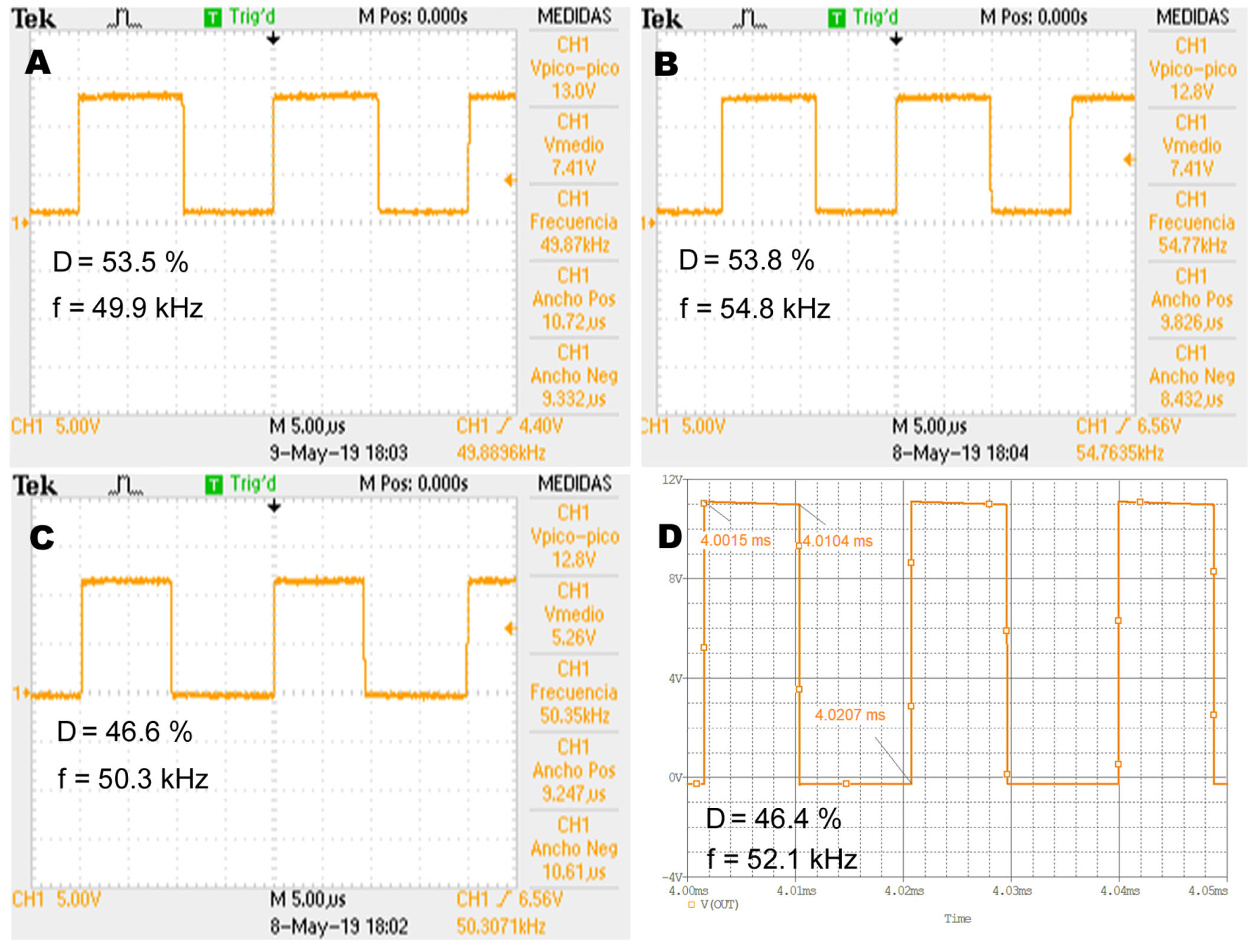
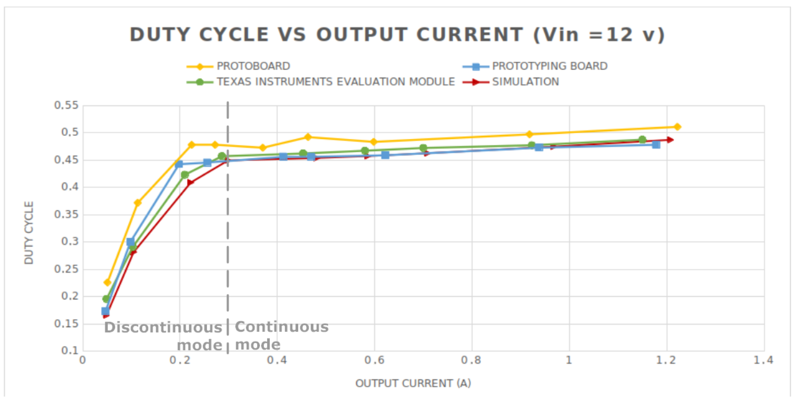
3.3.5. Duty Cycle Evolution Under Different Loads
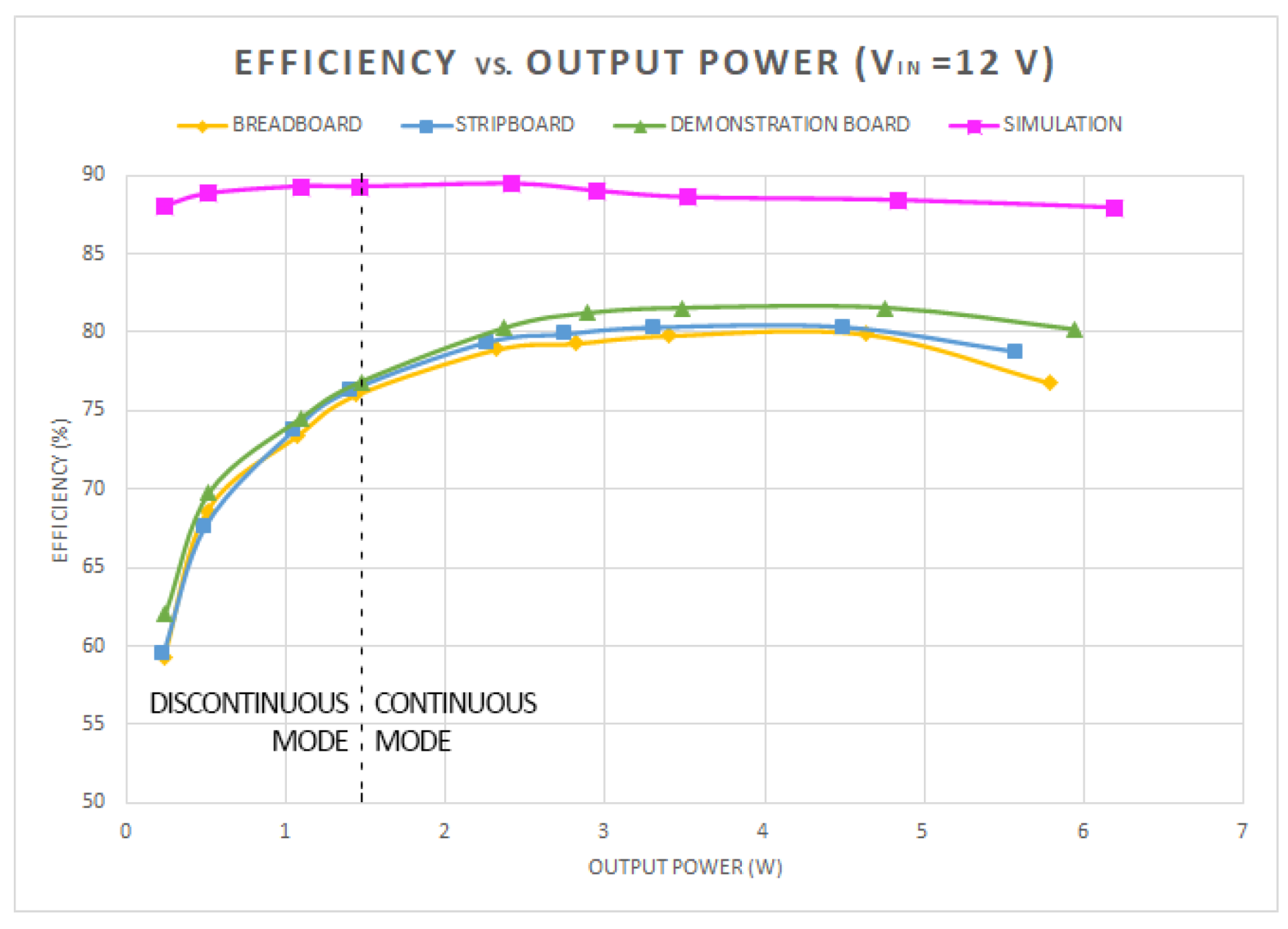
In this section, the experiment consisted of comparing the duty cycle waveform shape and frequency for the configurations under test and then analyzing the evolution of the duty cycle under different output currents. The duty cycle waveform was captured between the terminals of the freewheeling diode (pin two and ground in Figure 2).
Figure 9 shows the experimental and simulated results for the duty cycle signal considering the buck converter implemented in the breadboard, stripboard, and demonstration board, and the one simulated with PSpiceTM (Figure 9A, Figure 9B, Figure 9C, and Figure 9D, respectively) when load resistance was 5.04 Ω and the input voltage was 12 V. The sixth column of Table 3 summarizes the numerical results related to the duty cycle.
As is shown in Figure 9, the shape of both PWM signals was similar, as well as their frequency (Table 3). Indeed, the minimum measured frequency was for the buck converter mounted in a breadboard (49.9 kHz), while the maximum one was recorded for the stripboard (54.8 kHz). It is worthwhile to mention that although the nominal frequency for the LM2576-ADJ is 52 kHz—which is almost the value obtained by the simulation—results are still in line with the manufacturer, which specifies a frequency tolerance of ±10%.
The second part of the test was related to the duty cycle variation when the output current was modified by replacing the load resistor.
Figure 10 compares the evolution of the duty cycle and the output voltage when the output nominal current varied from 0.05 A to 1.26 A. The whole graph can be divided into two areas by the dashed line: continuous and discontinuous. Although a deeper analysis of the discontinuous mode is out of the scope of this paper, it must be said that for this mode, the duty cycle is smaller than for continuous mode [43]. Basically, less time is devoted to charging the inductor since a smaller amount of current is transferred through the converter, which is not enough to maintain the inductor current throughout the entire period [44].
In the right part of Figure 10, the converter provides more than 300 mA at the output and works in continuous mode. As is shown, the simulation, demonstration board, and stripboard exhibit a slightly lower duty cycle than the breadboard. Moreover, all of them follow the same tendency: the duty cycle increases when the output current also does. For a better understanding of what is happening in continuous mode, it is necessary to use Equation (3), which includes non-idealities of the components when the duty cycle is computed [45].
D = V o ( 1 + R c o i l R L ) + V F V i V o R D S o n R L + V F
where V i is the input voltage, V o is the input voltage, V F is the forward voltage of the freewheeling diode, R L is the load resistor, R c o i l is the resistance of the inductor, and R D S o n is the resistance between the drain and the source of the internal switching device. (The LM2576-ADJ has a BJT as an internal switching device. The internal resistance between the collector and the emitter is modelled by R D S o n , which causes the drop voltage V s a t mentioned in the datasheet).
Thus, an increase in output current is linked to a reduction in the output resistance ( R L ), which causes—according to the previous Equation (3)—the rise in the duty cycle shown in Figure 10. This increase also tries to compensate for the losses in the BJT and the coil to maintain the output voltage constant. Owing to the nature of the breadboard, the losses in this implementation are higher, and consequently, the duty cycle is higher (yellow line in Figure 10).

3.3.6. Efficiency

Electronic designers are increasingly concerned about efficiency, particularly regarding portable devices powered by batteries. The outstanding efficiency of DC-DC converters is one reason why linear regulators have fallen into disuse. Comparing the three different physical implementations under test provides relevant information regarding how this important feature can be affected.
Maximum experimental efficiency values obtained for each implementation and simulation circuit are gathered in the 8th column of Table 3. The evolution of efficiency has been analyzed by employing the variation in the output power. Figure 11 shows how the efficiency changes for the four configurations under study when the output power varies from 0.2 W to a value close to 6 W. The experiment was conducted by fixing the input voltage at 12 V and modifying the load resistor from 4.07 Ω to 101.49 Ω . The dashed line highlights the division between the continuous and discontinuous modes, which is triggered for a load resistor of 16.7 Ω .
The results show that the three physical configurations exhibited similar behaviour. The demonstration board achieved the best efficiency, closely followed by the configuration mounted in the stripboard and, finally, the breadboard implementation. This worse result for the buck converter implemented in the breadboard compared to the other configurations was expected due to the inefficient contacts of the breadboard. This problem is exacerbated when the current at the output is higher. Regardless, for output power values ranging between 2.5 W and 4.5 W, all the configurations reached an efficiency close to 80% or higher (up to 81.6% for the demonstration board). The results of the simulated circuit did not match those of the experimental ones. There are a wealth of reasons behind this misalignment. However, the losses related to defective contacts, the heat dissipation in the switching devices, and the parasite resistances linked to the coil and capacitors—equivalent series resistance (ESR)—are some of the reasons as to why the simulated efficiency was much higher than physical configurations.

3.3.7. Conducted EMI Analysis

To evaluate the impact of conducted EMI, the Total Harmonic Distortion (THD) at the output of each studied circuit was obtained. A FS300 spectrum analyzer by Rhode-Schwarz (Munich, Germany) was used to measure the harmonics. Although this instrument is not part of the basic equipment suggested in Section 2.2, its bandwidth ranging from 9 kHz to 3 GHz allowed for the analysis of the signal up to its tenth harmonic. The power spectra of the output signal for each analyzed circuit are presented in Figure 12, normalized in amplitude with respect to the fundamental harmonic and in the frequency range from 0 to 600 kHz. Due to the bandwidth limitations of the spectrum analyzer, the attenuation at low frequencies were corrected using a first-order bandpass filter model.
The computed THD are included in Table 3. As expected, the THD for the demonstration board is significantly better than the prototypes due to a careful layout design and its implementation with SMT components that minimize the area of loops with high switched currents. However, it is noteworthy that by following the recommendations of the DC-DC converter manufacturer, the stripboard and breadboard prototypes offer quality very close to the commercial board. These recommendations include minimizing inductance and ground loops, as well as keeping feedback connections short. It should be noted that the connection organization in the stripboard itself does not allow following these recommendations as faithfully as in the breadboard circuit, which may be reflected in a better THD value for the breadboard compared to the stripboard case.
Although the results regarding conducted EMI for breadboard and stripboard are not significantly worse than the demonstration one, the result can be enhanced by adding an LC filter with a low Q factor at the output, as is mentioned in the data sheet for the LM2576-ADJ by Texas Instruments.

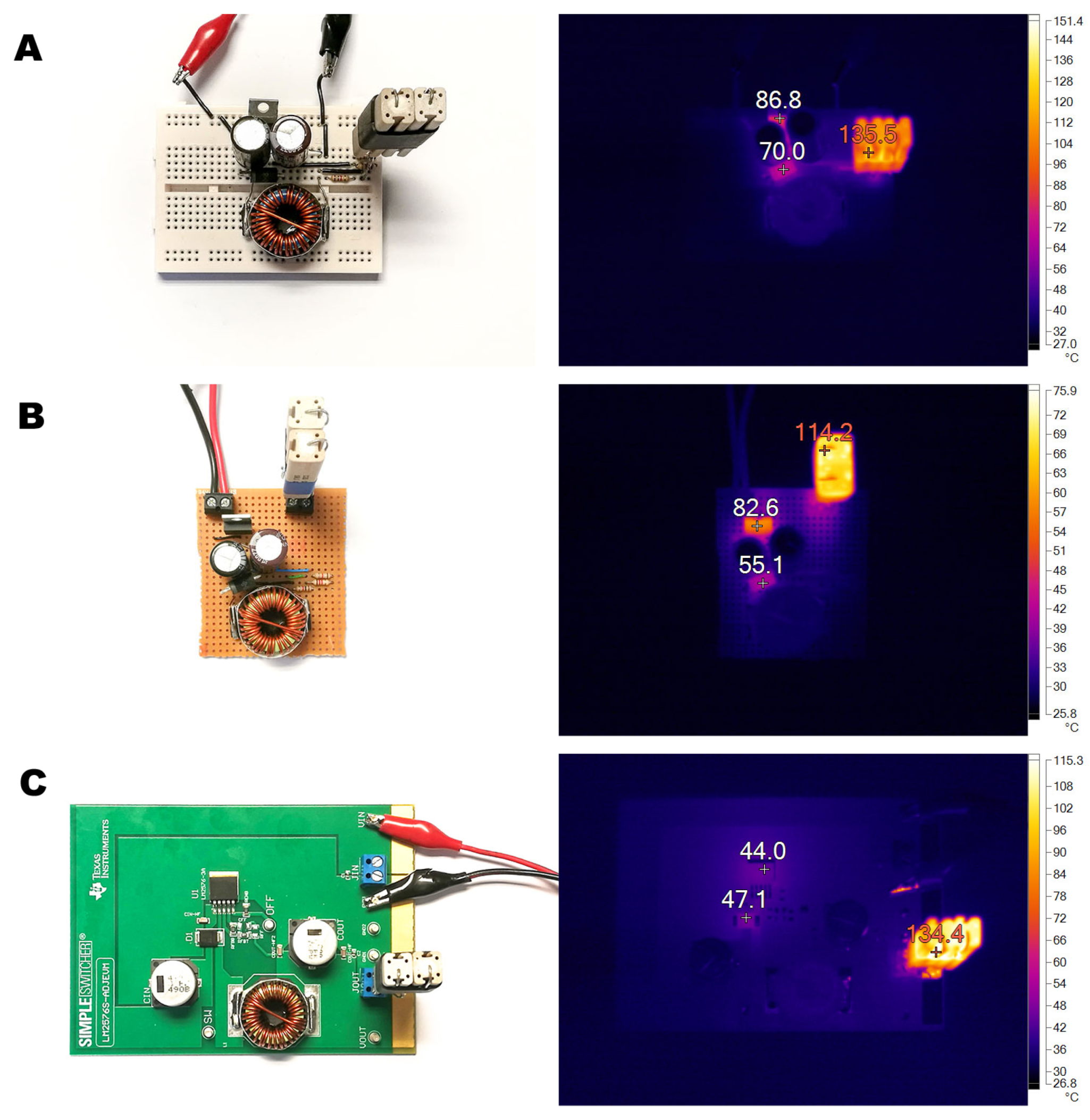
3.3.8. Thermal Study

The following study pursues a two-fold target. First, the theoretical temperature reached by the LM2577-ADJ and the freewheeling diode is estimated using the data provided by the manufacturer. The goal of this study is to understand whether these components exceed the limit temperature given by the manufacture. Although the reasons for the discrepancies between the theoretical and experimental temperatures are described, achieving an accurate estimation of the device temperature is out of the scope of this manuscript. Second, this thermal study attempts to carry out a comparison among the three physical designs, analyzing the causes of the differences found.
According to the datasheet of the LM2576-ADJ, the dissipated power ( P L M 2576 A D J in W) can be computed as follows:
P L M 2576 A D J = V i I Q + D I o V S a t
where V i is the applied input voltage (V), I Q is the quiescent current (A), D is the duty cycle (dimensionless), I o is the output current (A), and V S a t is the saturation voltage (V).
The thermal analysis was conducted with a nominal output current of 1 A after setting a load resistor of 5.04 Ω (5 W) and with 12 V at the input terminal. The experiment required keeping the DC-DC converter on for a long time until the temperature was stable. The drop voltage V s a t gathers all the losses related to the commutation of its internal bipolar transistor (Figure 2). This is the main source of heat for the IC. This value can be graphically obtained from Texas Instruments’ datasheet. For a given constant output voltage, V s a t increases when the output current also does. Additionally, the quiescent current ( I Q ) collects all the power consumption of the remaining internal functional blocks. The quiescent current linearly depends on the duty cycle, and its value can also be obtained from the datasheet.
According to the manufacturer’s datasheet and considering the input and output conditions previously mentioned, the values of V s a t and I Q are 1 V and 12 mA, respectively. The duty cycle needed for Equation (4) can be computed as the ratio V o / V i , that is, 0.42. The Equation (4) was applied to compute the power dissipated by the buck converter, obtaining 0.568 W.
Then, some considerations must be taken into account to theoretically estimate the temperature of the capsule of the integrated buck converter:
  • The values of R θ J A (junction temperature thermal resistance) and R θ J C (junction capsule thermal resistance) for TO-220 packages are 32.4 °C/W and 0.4 °C/W, respectively. In the case of SMT package (TO-263), R θ J A and R θ J C are 42.6 °C/W and 0.4 °C/W, respectively. It is important to clarify this point due to the discrepancies between thermal resistances provided by different manufacturers (Texas Instruments and Onsemi) for the same integrated circuit (LM2576-ADJ), since manufacturers follow different procedures to calculate these parameters [46].
  • Due to the small thermal resistance between junction and capsule (0.4 °C/W ), the temperature of the junction ( T J ) is going to be considered equal to the capsule ( T C ). Furthermore, the switching mode in which the buck converter works makes the value of R θ J C even smaller due to the existence of a thermal impedance which depends on the switching frequency.
  • The thermostated ambient temperature ( T A ) in the laboratory was considered constant at 26 °C for the whole duration of the experiment.
Finally, the junction temperature can be computed by Equation (5).
T J = T A + ( R θ J A × P L M 2576 A D J )
Thus, the theoretical values of the junction temperature for TO-220 (THT) and TO-263 (SMT) packages are 44.2 °C and 49.9 °C, respectively. Results regarding temperature are gathered in Table 4.
Another component likely to reach a high temperature is the freewheeling diode. Equation (6) defines its power dissipation:
P D i o d e = ( 1 D ) I o V F
where V F is the forward voltage of the diode.
This electronic component’s heat source is mainly linked to its internal resistance. Schottky diodes can work at higher frequencies than rectifying ones. Moreover, they exhibit a lower forward voltage (0.5 V for this application), which helps to reduce power dissipation. If initial considerations are taken into account and Equation (6) is applied, the theoretical power dissipated by the diode is 0.29 W.
According to the diode’s manufacturer, R θ J A and R θ J C are 25 °C/W and 10 °C/W, respectively, for the THT package and 115 °C/W and 10 °C/W, respectively, for the SMT device. Since the value of the thermal resistor between the junction and capsule is not negligible, the temperature of the capsule of the diode can be more accurately computed by Equation (7).
T C = T A + ( R θ C A × P D i o d e ) = T A + ( ( R θ J A R θ J C ) × P D i o d e )
Thus, the theoretical capsule temperature of the freewheeling diode is 30.5 °C for the THT package and 56.5 °C for the SMT version (Table 4).
Figure 13 includes the visible and infrared spectrum for the demonstration board (Figure 13A), stripboard implementation (Figure 13B), and buck converter mounted on a breadboard (Figure 13C). A set of temperature measurements was performed using K-type thermocouples at different accessible points across the circuit boards. This provided reference data for the adjustment of the emissivity of the surface to obtain more accurate measurements using the thermal imaging camera TiS55 by Fluke (Everett, DC, USA). Temperature monitoring started at circuit power-up, but only readings registered after thermal equilibrium was reached—approximately five minutes into operation—were considered for the study.
According to the results, as expected, the SMT version of the LM2576-ADJ installed in the demonstration board exhibited the lowest temperature of the implementations under study (44.0 °C). The value obtained was also around 6 °C below the theoretical one (49.9 °C). The reason behind this outstanding result is the role played by the PCB as a heatsink, which is enhanced by the use of 15 thermal vias [39]. As the manufacturer mentioned in the LM2576-ADJ datasheet, the square inches of copper area can significantly modify the final value of R θ J A , reducing the temperature of the junction. On the contrary, the THT version of the LM2576-ADJ reached 86.8 °C in the breadboard and 82.6 °C in the stripboard. The slightly lower temperature in the stripboard can be explained by the soldered pins and the dissipation effect of the straps of copper. However, there is a significant misalignment with the computed theoretical temperature of the LM2576-ADJ (44.2 °C). The IC manufacturer points out the lack of accuracy of computing the junction temperature by R θ J A , due to its dependency on factors such as altitude or PCB design, among others [46]. Moreover, manufacturers do not follow the same standards to compute R θ J A . Texas InstrumentsTM carries out procedures focused on electronic components placed on the PCB and provides thermal resistances where the PCB acts as a heatsink. These procedures are not necessary followed by other firms. As a result, for the same packages (TO-220 and TO-263) and same integrated circuit LM2576-ADJ, the brand OnsemiTM claims an R θ J A = 65 °C/W for its through-hole version (almost double compared to Texas InstrumentsTM). The last data of R θ J A is in line with the thermal resistance obtained by other manufacturers for integrated circuits with the TO-220 package, without any heatsink, and surrounded by still air. If this last value is used, the re-computation leads to a junction temperature of T J = 62.5 °C. Then, if the added effect of the rest of the components which surround the buck converter is considered [47], the theoretical estimated temperature must be closer to the experimental one. Indeed, the compactness and closeness in which components are placed—in order to achieve the layout requirements—impedes the airflow that goes through them. Furthermore, the physical circuits include a load ceramic resistance that reaches temperatures around 130 °C (Figure 13). This is a large source of heat that has a negative impact on the final temperature of the buck converter.
In short, the experimental temperatures achieved in the buck converters were below the limit of 150 °C for junction temperature recommended by Texas Instruments and Onsemi. Nevertheless, the junction temperature of the THT version of the LM2576-ADJ can be significantly reduced if a heatsink is added, which is a mechanically easy process for this package
The experimental results shown in Figure 13 related to the freewheeling diode indicate that again, the SMT version achieved a lower temperature (47.1 °C) compared to the THD diode mounted in the breadboard (70.0 °C) and stripboard (55.1 °C). The effect of the PCB acting as a heatsink explains the lower experimental temperature reached for SMT device. However, if this result is compared to its theoretical value (56.5 °C), the experimental result is lower. This is mainly linked to the conditions in which the value of R θ J A (115 °C/W) were computed. According to the datasheet of the B550C by Vishay, the junction ambient thermal resistor was evaluated for the maximum output current of the device (3 A), which is much more current than the experiment carried out in this paper (1 A). Consequently, the temperature is overestimated.
Figure 13 indicates that the temperature of the THT diode is higher in the breadboard than the stripboard, which can again be attributed to the soldered pins and the dissipation effect of the straps of copper of the stripboard. Regarding the differences between the experimental THT diode temperature and the theoretical computed value (30.4 °C), again, conditions by which the manufacturer measured R θ J A as well as the existence of components in the vicinity with high temperature (load resistance and buck converter) are the cause of these misalignments. For example, the STPS5L60 (twin component of the SB550 in terms of package and features), marketed by ST Microelectronics, exhibits a thermal resistance of R θ J A = 75 °C/W (three times higher than the one given by Vishay). Conditions in which the diode operates in the stripboard and the breadboard are not similar to the ones under which R θ J A was computed by the manufacturer, leading to the observed discrepancies.

4. Conclusions

This paper highlights the growing importance of non-isolated DC-DC buck converters in various emerging electronics applications, particularly in low-power and portable systems. In the early stages of the development of these products, the use of integrated circuits that encapsulate these devices in through-hole technology (THT) packages, rather than surface-mounted technology (SMT), is emphasized. This approach is particularly advantageous for rapid prototyping and proof-of-concept purposes using breadboards and stripboards.
Despite its high usability, there is a lack of information that guides the designer in their duty of implementing a fast prototype using a THT DC-DC converter. To cover this gap, this paper began by defining the most important characteristics that a THT buck converter should possess in order to correctly perform when mounted in a breadboard or stripboard. Once those features were determined, a wide market search was carried out to find the most appropriate commercial THT buck converters for fast prototyping. The market research was summarized in a comparative table. This represents an invaluable tool for designers and, by extension, professionals who want to prototype their designs based on buck converters on a breadboard.
The switching regulator LM2576-ADJ by Texas Instruments was the selected device for study, as it encompassed the most significant number of advantageous features. An experimental campaign using standard instruments commonly available in a higher education laboratory was conducted to experimentally check the validity of the outcomes obtained with the LM2576-ADJ. To quantify the limitations of fast prototyping using THT components, the experimental study was carried out as a comparative analysis. Thus, simulation and experimental results were successfully compared from three physical implementations: buck converter mounted on a breadboard, buck converter mounted in a stripboard (with their components soldered), and demonstration board marketed by the manufacturer.
The compared results showed that the buck converter based on the LM2576-ADJ and mounted in a breadboard works remarkably well when points such as line and load regulation, duty cycle, and efficiency were tested in the laboratory. In contrast, the designer has to be aware of some issues when using a breadboard, such as higher voltage ripple and drop voltage. Imperfections caused by parasitic resistors or capacitors are responsible for these setbacks. As a result of these imperfections, the duty cycle of the converters mounted in the breadboard and stripboard was slightly higher (by 10%) than in simulations and the demonstration board for the same output current. This weak increase is also connected to a small efficiency decrease for these fast implementations.
Finally, a thermal study was conducted. Results showed that although the temperature of components from the breadboard and stripboard was higher than SMT ones, this increase did not cause any harm to any of the THT components.

Author Contributions

Conceptualization, J.V.M. and L.P.-L.; methodology, J.V.M., A.G.G.-R. and J.D.A.-P.; software: OrCADTM PSpiceTM V.17.2 and FrizingTM V.0.9.10, L.P.-L. and L.M.N.-N.; validation, L.P.-L. and J.V.M.; formal analysis, J.V.M. and L.P.-L.; investigation, J.D.A.-P., J.V.M. and L.P.-L.; resources, L.M.N.-N.; data curation, J.V.M. and L.P.-L.; writing—original draft preparation, J.V.M. and L.M.N.-N.; writing—review and editing, A.G.G.-R. and L.M.N.-N.; visualization, A.G.G.-R.; supervision, J.V.M.; project administration, J.V.M. and L.P.-L.; funding acquisition, J.V.M., L.M.N.-N., A.G.G.-R., L.P.-L. and J.D.A.-P. All authors have read and agreed to the published version of the manuscript.

Funding

This research was partly funded by the University of Jaen by innovation teaching project tittle: “Canal de vídeos en inglés y herramienta de evaluación online para el aprendizaje autónomo del entorno de programación LabVIEW” with code: PIMED21 202224.

Data Availability Statement

Data are contained within the article.

Conflicts of Interest

The authors declare no conflicts of interest.

References

  1. Savekar, A.; Wankhede, S.; Kumar, V. DC-DC Converter Market. Global Opportunity Analysis and Industry Forecast, 2020–2027. Allied Markey Research, Report Code: A05304, October 2020. Available online: https://www.alliedmarketresearch.com/press-release/dc-dc-converter-market.html (accessed on 1 February 2025).
  2. Luo, P.; Peng, D.; Wang, Y.; Zheng, X. Review of Solar Energy Harvesting for IoT Applications. In Proceedings of the 2018 IEEE Asia Pacific Conference on Circuits and Systems (APCCAS), Chengdu, China, 26–30 October 2018; pp. 512–515. [Google Scholar] [CrossRef]
  3. Dileep, G.; Singh, S.N. Selection of non-isolated DC-DC converters for solar photovoltaic system. Renew. Sustain. Energy Rev. 2017, 76, 1230–1247. [Google Scholar] [CrossRef]
  4. Swaminathan, N.; Cao, Y. An Overview of High-Conversion High-Voltage DC-DC Converters for Electrified Aviation Power Distribution System. IEEE Trans. Transp. Electrif. 2020, 6, 1740–1754. [Google Scholar] [CrossRef]
  5. Martínez-Heredia, J.M.; Colodro, F.; Mora-Jiménez, J.L.; Remujo, A.; Soriano, J.; Esteban, S. Development of GaN Technology-Based DC/DC Converter for Hybrid UAV. IEEE Access 2020, 8, 88014–88025. [Google Scholar] [CrossRef]
  6. Chakraborty, S.; Vu, H.-N.; Hasa, M.M.; Tran, D.-D.; Baghdadi, M.E.; Hegazy, O. DC-DC Converter Topologies for Electric Vehicles, Plug-in Hybrid Electric Vehicles and Fast Charging Stations: State of the Art and Future Trends. Energies 2019, 12, 1569. [Google Scholar] [CrossRef]
  7. Jørgensen, K.L.; Zhang, Z.; Andersen, M.A.E. Next generation of power electronic-converter application for energy-conversion and storage units and systems. Clean Energy 2019, 3, 307–315. [Google Scholar] [CrossRef]
  8. Xiao, J.; Peterchev, A.V.; Zhang, J.; Sanders, S.R. A 4-/spl mu/a quiescent-current dual-mode digitally controlled buck converter IC for cellular phone applications. IEEE J. Solid-State Circuits 2004, 39, 2342–2348. [Google Scholar] [CrossRef]
  9. Chen, G.; Hanson, S.; Blaauw, D.; Sylvester, D. Circuit Design Advances for Wireless Sensing Applications. Proc. IEEE 2010, 98, 1808–1827. [Google Scholar] [CrossRef]
  10. Baharudin, N.H.; Mansur, T.M.N.T.; Hamid, F.A.; Misrun, M.I. Performance Analysis of DC-DC Buck converter for renewable energy application. In Proceedings of the 1st International Conference on Green and Sustainable Computing (IGoGeS), Pittsburgh, PA, USA, 24–25 October 2017; Available online: https://iopscience.iop.org/article/10.1088/1742-6596/1019/1/012020/pdf (accessed on 1 February 2025).
  11. Mostafa, T.M.; Muharam, A.; Hattori, R. Wireless battery charging system for drones via capacitive power transfer. In Proceedings of the 2017 IEEE PELS Workshop on Emerging Technologies: Wireless Power Transfer (WoW), Chongqing, China, 20–22 May 2017; pp. 1–6. [Google Scholar] [CrossRef]
  12. Mathúna, C.Ó.; Wang, N.; Kulkarni, S.; Roy, S. Review of Integrated Magnetics for Power Supply on Chip (PwrSoC). IEEE Trans. Power Electron. 2012, 27, 4799–4816. [Google Scholar] [CrossRef]
  13. Coleman, W.E.; Jean, D.; Bradbury-Bennett, J.R. Stencil design for mixed technology through-hole/SMT placement and reflow. Solder. Surf. Mt. Technol. 2000, 12, 8–12. [Google Scholar] [CrossRef]
  14. He, J.; Cen, Y.; Alelaumi, S.; Won, D. An Artificial Intelligence-Based Pick-and-Place Process Control for Quality Enhancement in Surface Mount Technology. IEEE Trans. Compon. Packag. Manuf. Technol. 2022, 12, 1702–1711. [Google Scholar] [CrossRef]
  15. Nguty, T.A.; Philpott, J.D.; Ekere, N.N.; Teckle, S.; Salam, B.; Rajkumar, D. Rework techniques process evaluation for chip scale packages. IEEE Trans. Electron. Packag. Manuf. 2000, 23, 200–207. [Google Scholar] [CrossRef]
  16. He, W. Analysis on the Component Movement in Electronic Assembly. In Proceedings of the 2021 8th International Forum on Electrical Engineering and Automation (IFEEA), Xi’an, China, 3–5 September 2021; pp. 116–119. [Google Scholar] [CrossRef]
  17. Houari, B.; Aissa, B.; Lakhdar, L.; Yazid, B.E. DC/DC buck Converter Prototype for Educational Nanosatellite Power Sub-System. In Proceedings of the 2023 International Conference on Advances in Electronics, Control and Communication Systems (ICAECCS), Blida, Algeria, 6–7 March 2023; pp. 1–6. [Google Scholar] [CrossRef]
  18. Rai, J.N.; Gupta, N.; Bansal, P. Design and analysis of DC-DC boost converter. Int. J. Adv. Res. Innov. 2016, 4, 499–502. [Google Scholar] [CrossRef]
  19. Eguchi, K.; Rubpongse, R.; Shibata, A.; Ishibashi, T. Synthesis and analysis of a cross-connected Fibonacci dc/dc converter with high voltage gain. Energy Rep. 2020, 6, 130–136. [Google Scholar] [CrossRef]
  20. Collins, N.; Lonergan, S. Solder Up! From Breadboard to Circuit Board. In Handmade Electronic Music; Routledge: London, UK, 2020. [Google Scholar]
  21. Hamblen, J.O.; van Bekkum, G.M.E. An Embedded Systems Laboratory to Support Rapid Prototyping of Robotics and the Internet of Things. IEEE Trans. Educ. 2013, 56, 121–128. [Google Scholar] [CrossRef]
  22. Wang, C.; Yeh, H.-M.; Wang, B.; Wu, T.-Y.; Tsai, H.-R.; Liang, R.-H.; Hung, Y.-P.; Chen, M.Y. CircuitStack: Supporting Rapid Prototyping and Evolution of Electronic Circuits. In Proceedings of the 29th Annual Symposium on User Interface Software and Technology (UIST ’16), Tokyo, Japan, 16–19 October 2016; pp. 687–695. [Google Scholar] [CrossRef]
  23. Ferreiro, A.L.; Simón, A.R.A.; Casas, S.L.; Meléndez, A.A.N. A current-controlled DC-to-DC switch mode power converters emulator software. In Proceedings of the 2016 Technologies Applied to Electronics Teaching, TAEE, Seville, Spain, 22–24 June 2016. [Google Scholar] [CrossRef]
  24. Zaitsu, R. Voltage Mode Boost Converter Small Signal Control Loop Analysis Using the TPS61030; Application Report; Texas Instruments: Dallas, TX, USA, 2007; pp. 1–21. [Google Scholar]
  25. Crowel, G. How Much Power and How High of a Frequency Can a Breadboard Handle? From Circuit Bread.com. Available online: https://www.circuitbread.com/ee-faq/how-much-power-and-how-high-of-a-frequency-can-a-breadboard-handle (accessed on 10 April 2022).
  26. Wikipedia. The Free Encyclopedia. Breadboard. Available online: https://en.wikipedia.org/wiki/Breadboard (accessed on 1 February 2025).
  27. Musunuri, S.; Chapman, P.L.; Zou, J.; Liu, C. Inductor design for monolithic DC-DC converters. In Proceedings of the IEEE 34th Annual Conference on Power Electronics Specialist, 2003, PESC ’03, Acapulco, Mexico, 15–19 June 2003; Volume 1, pp. 227–232. [Google Scholar] [CrossRef]
  28. Crane, L. Selecting the Best Inductor for a DC-DC Converter. Craftcoil, Application Notes, Document 469-1, July 2017. Available online: https://www.coilcraft.com/getmedia/d4009ece-69be-49a6-9185-9cbacb65e3aa/Doc469_selecting_inductors.pdf (accessed on 1 February 2025).
  29. IPC-2221C—Association Connecting Electronics Industries. Generic Standard on Printed Board Design. 2024. Available online: https://shop.ipc.org/ipc-2221/ipc-2221-standard-only/Revision-c/english (accessed on 1 February 2025).
  30. Zhang, H.J. PCB Layout Considerations for Non-Isolated Switching Power Supplies, Analog Application Note 136 (AN136-1), June 2012. pp. 1–14. Available online: https://www.analog.com/en/resources/app-notes/an-136.html (accessed on 1 February 2025).
  31. Kollman, R. Constructing Your Power Supply: Layout Considerations; Texas Instruments Application Note SLUP230; Texas Instruments Inc.: Dallas, TX, USA, 2005. [Google Scholar]
  32. Kulkarni, S.; Bangade, S.; Khadse, M.; Waghulde, D.; Aher, P.; Gaikwad, K.; Thakurdesai, S. Design and optimization of the on board DC/DC converters of Swayam satellite. In Proceedings of the 2014 IEEE International Conference on Power Electronics, Drives and Energy Systems (PEDES), Mumbai, India, 16–19 December 2014; pp. 1–6. [Google Scholar] [CrossRef]
  33. Glaser, C. Five steps to a great PCB layout for a step-down converter. In Analog Applications Journal; Texas Instruments Inc.: Dallas, TX, USA, 2015; Available online: https://www.ti.com/lit/an/slyt614/slyt614.pdf?ts=1742720268015 (accessed on 1 February 2025).
  34. Bhargava, A.; Pommerenke, D.; Kam, K.W.; Centola, F.; Lam, C.W. DC-DC Buck Converter EMI Reduction Using PCB Layout Modification. IEEE Trans. Electromagn. Compat. 2011, 53, 806–813. [Google Scholar] [CrossRef]
  35. Ott, H. Electromagnetic Compatibility Engineering; John Wiley and Sons: New York, NY, USA, 2009. [Google Scholar]
  36. Ott, H. Noise Reduction Techniques in Electronic Systems, 2nd ed.; John Wiley and Sons: Chichester, UK, 1988. [Google Scholar]
  37. Simpson, C. Linear and Switching Voltage Regulator Fundamental Part 1. Texas Instruments. Available online: https://www.ti.com/lit/an/snva559/snva559.pdf (accessed on 1 February 2025).
  38. Tucker, J. Understanding output voltage limitations of DC/DC buck converters. In Analog Applications Journal; Texas Instruments Inc.: Dallas, TX, USA, 2008; Available online: https://www.ti.com/lit/an/slyt293/slyt293.pdf?ts=1742730170338&ref_url=https%253A%252F%252Fwww.google.com%252F (accessed on 1 February 2025)High-Performance Analog Products.
  39. Texas Instruments, LM2576S-ADJEVM User’s Guide. User’s Guide SNVU527, June 2016. Available online: https://www.ti.com/lit/pdf/snvu527 (accessed on 1 February 2025).
  40. Chew, L.W. The effect of higher order model decoupling capacitors in the design of a power delivery network. In Proceedings of the 2012 4th Asia Symposium on Quality Electronic Design (ASQED), Penang, Malaysia, 10–11 July 2012; pp. 117–122. [Google Scholar] [CrossRef]
  41. Erickson, R.W.; Maksimović, D. Fundamentals of Power Electronics; Springer: Berlin/Heidelberg, Germany, 2020. [Google Scholar]
  42. Himmelstoss, F.A.; Edelmoser, K.H. Concept to reduce the ringing during the discontinuous mode of a DC/DC converter. In Proceedings of the 2017 19th International Conference on Electrical Drives and Power Electronics (EDPE), Dubrovnik, Croatia, 4–6 October 2017; pp. 106–111. [Google Scholar] [CrossRef]
  43. Hart, D.W. Power Electronics; McGraw-Hill Companies Inc.: New York, NY, USA, 2010. [Google Scholar]
  44. Texas Instruments. Understanding Buck Power Stages in Switchmode Power Supplies. Application Report SLVA057, March 1999. Available online: https://www.ti.com/lit/an/slva057/slva057.pdf (accessed on 1 February 2025).
  45. Mohan, G.M.; Mukesh, P.; Yogesh, H. Effect of Non-Idealities on the Design and Performance of a DC-DC Buck Converter. J. Power Electron. 2016, 16, 832–839. [Google Scholar] [CrossRef]
  46. Edwards, D.; Nguyen, H. Semiconductor and IC Package Thermal Metrics; Texas Instruments Application Note SPRA953D; Texas Instruments Inc.: Dallas, TX, USA, 2003. [Google Scholar]
  47. Lall, B.S.; Guenin, B.M.; Molnar, R.J. Methodology for thermal evaluation of multichip modules. In Proceedings of the 1995 IEEE/CPMT 11th Semiconductor Thermal Measurement and Management Symposium (SEMI-THERM), San Jose, CA, USA, 7–9 February 1995; pp. 72–79. [Google Scholar] [CrossRef]
Figure 1. General block diagram of a non-isolated buck converter with its constitutive parts.
Electronics 14 01273 g001
Figure 2. Schematic of a non-isolated buck converter based on the integrated switching regulator LM2576-ADJ. Internal block schematic of LM2576-ADJ extracted from Texas Instruments’ datasheet.
Electronics 14 01273 g002
Figure 3. Images of the physical buck implementations tested and based on LM2576-ADJ: (A) breadboard implementation, (B) stripboard implementation, and (C) demonstration board LM2576S-ADJEVM by Texas Instruments.
Electronics 14 01273 g003
Figure 4. Simplified schematic of buck converter LM2576-ADJ under study mounted on a breadboard. Circuit powered by Frizing TM V.0.9.10 by Interaction Design Lab (Postdam, Germany).
Electronics 14 01273 g004
Figure 5. Output voltage ripple results for implementations on a breadboard (A), stripboard (B), and demonstration board (C), as well as results obtained by simulation software (D). The vertical scale is set to 20 mV/div in (A), and 5 mV/div in (BD).
Electronics 14 01273 g005
Figure 6. (A) Line regulation results for the three physical implementations under study based on LM2576-ADJ: breadboard (yellow), stripboard (blue), and demonstration board (green line), as well as line regulation obtained by simulation software (pink). (B) Load regulation results for the three physical implementations: breadboard (yellow), stripboard (blue), and demonstration board (green), as well as load regulation obtained by simulation software (pink).
Electronics 14 01273 g006
Figure 7. Results for the implementation mounted in the breadboard (A) and simulated circuit (B). The duty cycle (blue lines) and the current across the buck converter’s inductance (orange lines) work in continuous mode.
Electronics 14 01273 g007
Figure 8. Voltage across the freewheeling diode and current across the inductance ( i L ( t ) ) of the buck converter under study when the load resistance is 47.15 Ω (output current less than 300 mA) and the discontinuous mode is triggered. Results for the implementation mounted in the breadboard (A) and simulated circuit (B).
Electronics 14 01273 g008
Figure 9. Duty cycle transient results for the three physical implementations under study based on LM2576-ADJ breadboard (A), stripboard (B), and demonstration board (C), as well as simulation software (D).
Electronics 14 01273 g009
Figure 10. Evolution of the duty cycle with the output current when the output current varies for the different implementations: breadboard (yellow), stripboard (blue), demo-board (green), and simulation (purple). The dashed line represents the limit between the continuous and discontinuous modes.
Electronics 14 01273 g010
Figure 11. Experimental and simulated efficiency results for the three physical implementations under study based on LM2576-ADJ: breadboard (yellow), stripboard (blue), and demonstration board (green), as well as simulation software (pink).
Electronics 14 01273 g011
Figure 12. Spectral measurements of the output for the physical circuits under study.
Electronics 14 01273 g012
Figure 13. Thermal analysis carried out for the three implementations under study. Images (AC) correspond to the implementation of the breadboard, stripboard, and demonstration board, respectively.
Electronics 14 01273 g013
Table 1. Results from the market research conducted among five different brands to identify the most suitable non-isolated DC-DC converter for fast prototyping.
ManufacturerModelInputOutput Package LimitedPrice/Simulation
Voltage Voltage Maximun Output Maximun Evaluation Number Units Tools Supplier
(Min/ (Min/ Output Type Switching Module of External (*) Availability Availability
Max) Max) Current Frequency Availability Components (**) (***)
Linear Technology (now Analog Devices)LT10748/45 V8/35 V5 ATO-220Adjustable110 kHzNoYes15.86 €/1 (‡)iii2, 3, 4
LT1074HV8/64 V8/45 V5 ATO-220Adjustable125 kHzNoYes18.76 €/1 (‡)iii2, 3, 4
LT10768/45 V8/35 V2 ATO-220Adjustable110 kHzNoYes10.35 €/1 (‡)iii2, 3, 4
LT1076HV8/64 V8/45 V2 ATO-220Adjustable125 kHzNoYes16,12 €/1 (‡)iii2, 3, 4
Maxim (now Analog Devices)MAX638AMJA/883B2.2/16.5 V1.25/16 V525 mADIP-8Adjustable65 kHzNoYes (†)25.00 €/1-4
MAX5035BUPA7.5/76 V1.25/13.2 V1 ADIP-8Fixed/Adjustable125 kHzYesYes3.80 €/1ii4
MAX758ACPA+4/16 V1.25/16 V750 mADIP-8Fixed/Adjustable190 kHzNoYes10.62 €/1 (‡)-3, 4
ON SemiconductorLM25744/40 V1.23/37 V500 mADIP-8Fixed52 kHzNoYes1.74 €/1i1, 2, 3, 4
LM2576/LM2576-ADJ4/40 V1.23/37 V3 ATO-220Fixed/Adjustable52 kHzNoYes2.56 €/5i1, 2, 3, 4
LM2575/LM2575-ADJ4/40 V1.23/37 V1 ATO-220Fixed/Adjustable52 kHzNoYes2.29 €/1i1, 2, 3, 4
ST MicroelectronicsL296/L296P9/46 V5.1/40 V4 AMultiwatt 15 LFixed/Adjustable200 kHzNoNo ( )( )13.58 €/1ii1, 2, 3, 4
L4970A15/50 V5.1/40 V10 AMultiwatt 15 LFixed200 kHzNoNo ( )15.23 €/1ii1, 2, 3, 4
L4975A15/50 V5.1/40 V5 AMultiwatt 15 LFixed200 kHzNoNo ( )17.86 €/1ii1, 2
Texas InstrumentsLM25744/40 V1.23/37 V500 mADIP-8Fixed/Adjustable52 kHzNoYes3.59 €/1i, iii1, 2, 3, 4
LM2574HV4/60 V1.23/37 V500 mADIP-8Fixed/Adjustable52 kHzNoYes4.46 €/1ii, iii1, 3, 4
LM25764/40 V3.33/37 V3 ATO-220Fixed/Adjustable52 kHzYesYes3.40 €/5i, iii1, 2, 3, 4
LM2576HV4/60 V3.33/37 V3 ATO-220Fixed/Adjustable52 kHzNoYes9.55 €/1ii, iii1, 2, 3, 4
LM25754/40 V3.33/37 V1 ATO-220Fixed/Adjustable100 kHzYesYes3.58 €/1i, iii1, 2, 3, 4
LM2575HV4/40 V3.33/57 V1 ATO-220Fixed/Adjustable100 kHzNoYes5.73 €/1ii, iii1, 2, 3, 4
LM25954.75/40 V1.2/37 V1 ATO-220Fixed/Adjustable150 kHzNoYes4.38 €/1ii, iii3, 4
LM25964.75/40 V1.2/37 V3 ATO-220Fixed/Adjustable150 kHzYesYes5.52 €/1ii, iii1, 2, 3, 4
Observations and notes: (*) Price in EUR for a single device (VAT included)/Minimum number of units to be ordered; (**) i means simulation model is available in OrCADTM PSpiceTM; ii means the model can be downloaded from the manufacturer’s website; iii means the model can be simulated online. (***) 1,2,3 and 4 refer to the availability of the device on the RS, Farnell, Mouser, and Digi-Key web pages, respectively; (†) Includes an internal circuit to control the state of charge of a battery; ( ) It should be noted that this buck converter has an extra current limiter circuitry; ( ) Although the IC’s package has 15 pins, not all of them must be connected to make the circuit work; (‡) The price of this device was extracted from the web page of the first distributor indicated in column 13 due to the lack of availability in RS Amidata.
Table 2. List of components surrounding the IC LM2576-ADJ used in the two fast prototypes mounted in a breadboard and stripboard.
DeviceDescriptionManufacturerPart Number
DDiode, Schottky, 50 V, 5 A,On semiconductorSB550
LInductor, Toroid, 100 µH, 6.1 A, 0.035 Ω Bourns (Riverside, CA, USA)PM2120-101K-RC
C i n CAP, AL, 470 µF, 63 V, ±20%, 0.053 Ω Panasonic (Kadoma, Japan)EEUFC1J471
C o u t CAP, AL, 2200 µF, 63 V, ±20%, 0.028 Ω PanasonicEEUFC1E222S
R11 k Ω resistor, 5%, 0.25 WRS PRO (London, UK)707-7666
R21.2 k Ω and 1.8 k Ω resistors in series, 5%, 0.25 WRS PRO707-7678, 739-7471
Table 3. Summary of the most important experimental results carried out during the comparison of the three physical-mirrored DC-DC buck converters and the simulated circuit.
Voltage
Ripple
Line
Regulation
Load
Regulation
Switching
Frequency
Duty
Cycle
Maximum
Efficiency
THDLM2576-ADJ
Temperature
Breadboard57.6  m V p k p k 0.37 %0.33%49.9 kHz53.5%79.9%1.02%86.8 °C
Stripboard17.2  m V p k p k 0.32 %0.79%54.8 kHz53.8%80.3%1.12%82.6 °C
Demonstration board19.0  m V p k p k 0.30%0.06%50.3 kHz46.6%81.6%0.45%44.0 °C
Simulation11.8  m V p k p k 0.28 %0.04%52.1 kHz46.4%89.5%
Table 4. Summary of the theoretical and experimental capsule temperatures reached for the LM2676-ADJ and the freewheeling diode.
Theoretical Temperature
TO220 Package
Theoretical Temperature
SMT Package
BreadboardStripboardDemonstration
Board
LM2576-ADJ44.2 °C49.9 °C86.8 °C82.6 °C44.0 °C
Freewheeling diode30.4 °C56.5 °C70.0 °C55.1 °C47.1 °C
Disclaimer/Publisher’s Note: The statements, opinions and data contained in all publications are solely those of the individual author(s) and contributor(s) and not of MDPI and/or the editor(s). MDPI and/or the editor(s) disclaim responsibility for any injury to people or property resulting from any ideas, methods, instructions or products referred to in the content.

