Article

Image Classification in Memristor-Based Neural Networks: A Comparative Study of Software and Hardware Models Using RRAM Crossbars

Aix-Marseille University, CNRS, IM2NP, 5 Rue Enrico Fermi, CEDEX 20, 13451 Marseille, France
Electronics 2025, 14(6), 1125; https://doi.org/10.3390/electronics14061125
Submission received: 17 January 2025 / Revised: 6 February 2025 / Accepted: 13 February 2025 / Published: 12 March 2025
(This article belongs to the Special Issue Intelligent Computing Technology Based on New Types of Memristors)

Abstract

:
Vector–matrix multiplication (VMM), which dominates the computational workload in neural networks, accounts for over 99% of all operations, particularly in Convolutional Neural Networks (CNNs). These operations, consisting of multiply-and-accumulate (MAC) functions, are straightforward but demand massive parallelism, often involving billions of operations per layer. This computational demand negatively affects processing time, energy consumption, and memory bandwidth due to frequent external memory access. To efficiently address these challenges, this paper investigates the implementation of a full neural network for image classification, using TensorFlow as a software baseline, and compares it with a hardware counterpart mapped onto resistive RAM-based crossbar arrays, a practical implementation of the memristor concept. By leveraging the inherent ability of RRAM crossbars to perform VMMs in a single step, we demonstrate how RRAM-based neural networks can achieve efficient in-memory analog computing. To ensure realistic and practical results, the hardware implemented utilizes RRAM memory cells characterized through silicon measurements. Furthermore, the design exclusively considers positive weights and biases to minimize the area overhead, resulting in a lightweight hardware solution. This approach achieves an energy consumption of 190 fJ/MAC operation for the crossbar array, highlighting its efficiency in power-constrained applications despite a drop in the prediction confidence of 27.5% compared to the software approach.

1. Introduction

The traditional von Neumann (VN) computing architecture is reaching critical limitations, particularly regarding energy efficiency and latency [1]. This is particularly true when dealing with the vast amount of data generated by IoT devices, self-driving cars, cloud computing, etc. [2]. This situation, known as the “memory wall”, refers to the growing gap between the speed of a computer’s processing units and the slower access speed of memory, resulting in a critical performance bottleneck [3]. This limitation of modern computing architectures encourages the investigation of different processing paradigms, which are categorized as non-von Neumann (non-VN).
Over the last few years, there has been a lot of activity across research groups proposing efficient hybrid “CMOS-nanodevice” computing hardware architectures such as Artificial Neural Networks (ANNs) [4]. ANNs have demonstrated impressive performances in recognition tasks where classical VN hardware architectures have difficulties classifying or organizing data, a task that the human brain seems to accomplish efficiently. The architecture of ANNs is inspired by biological neural networks. ANNs consist of numerous units that are organized in a specific configuration to facilitate communication among them. These units are commonly known as nodes or neurons. Neurons utilize connection pathways known as synapses to communicate with each other, with each synapse assigned a specific weight that influences the strength of its signal transmission. These weights can either amplify or inhibit the signals transmitted across the network. Consequently, an ANN can be seen as a complex adaptive system, capable of modifying its internal parameters [5].
Emerging Back End Of Line (BEOL) resistive memory devices such as RRAMs [6,7] are considered to be the optimal candidates to emulate synaptic behavior at the nanometer scale, as they offer the ability to modulate their conductance in addition to being easily integrated with CMOS-based neuron circuits [8,9]. Among the different RRAM technologies available, oxide-based RAMs (OxRAMs) have proven to be very effective in implementing some aspects of synaptic plasticity [10,11]. Vector–matrix multiplication (VMM) in the context of RRAM-based ANNs involves performing calculations using the different conductance states of the RRAM cells [12]. In their crossbar architecture, input vectors are represented as voltage signals applied to the rows of the crossbar, while the weight matrix is stored as conductance values in the RRAM cells. When voltages are applied to the rows, the resulting currents through each cell are proportional to the product of the input voltage and the cell’s conductance, enabling the simultaneous computation of weighted sums across multiple columns of the crossbar array. In this context, this work evaluates the ability of a crossbar RRAM array to perform VMM as part of an image processing application. The main contributions of the proposed study are as follows:
  • The conductance modulation capability of actual RRAM cells is evaluated at the test chip level through electrical characterization.
  • At the software level, an ANN model is defined and trained for image classification, and its model parameters (weights and biases) are generated.
  • At the hardware level, the ANN model parameters are mapped to a physical RRAM crossbar array, taking into account the RRAM cell characteristics extracted from silicon measurements.
  • The RRAM crossbar array is simulated to demonstrate its ability to perform vector-matrix–multiplication (VMM) directly in the analog domain.
The remainder of this paper is organized as follows: Section 2 details the specifications of the fabricated RRAM cells and evaluates the conductance modulation capabilities of the selected RRAM technology. Section 3 presents the ANN weight mapping methodology used, focusing on a two-layer neural network designed for image classification. Section 4 describes the hardware-level implementation of the neural network using RRAM technology and evaluates its performance. Section 5 discusses the obtained results, and, finally, Section 6 concludes this paper.

2. Background

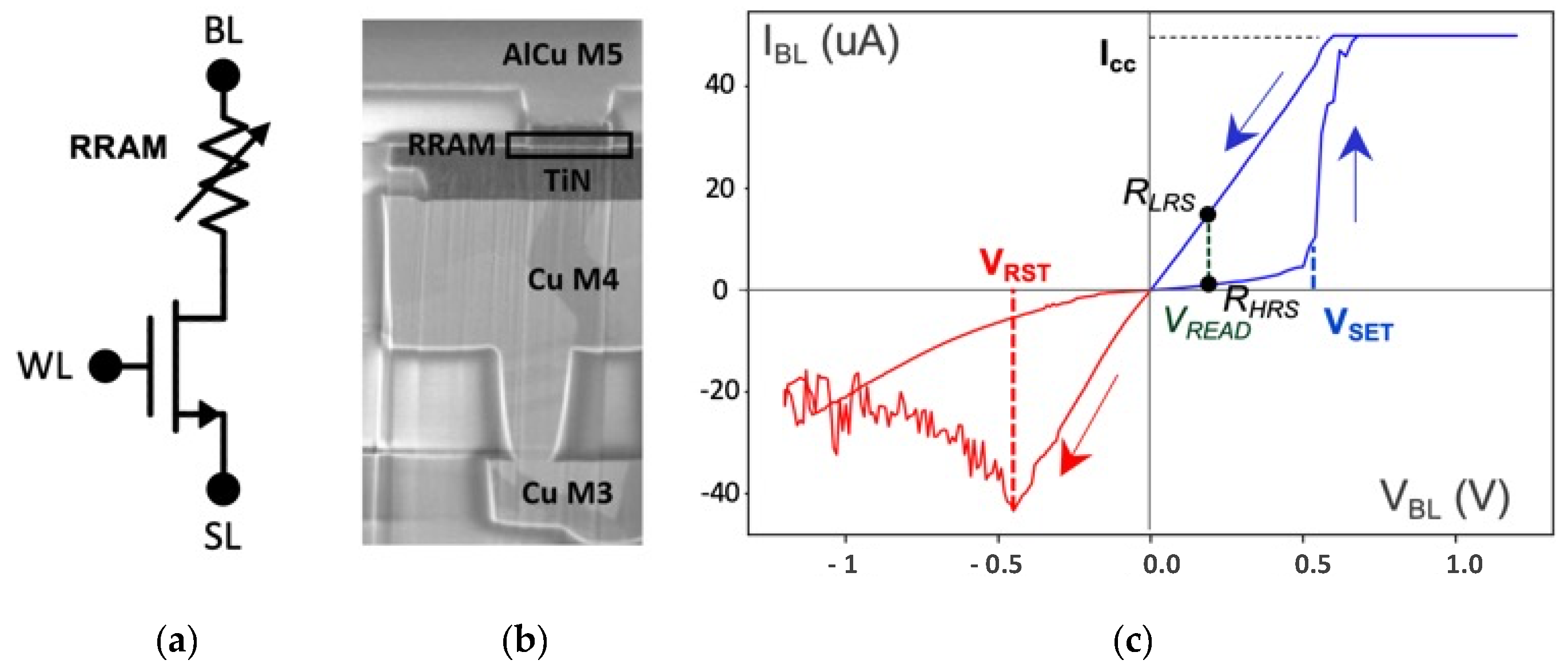
2.1. Specifications of the Manufactured RRAM Cells

RRAM devices typically operate based on the reversible change in resistance caused by the formation and rupture of conductive filaments (CFs) [13]. From a physical standpoint, when a voltage is applied across the cell (i.e., between the top and bottom electrodes), depending on the voltage polarity, one or more CFs made out of oxygen vacancies are either formed or ruptured. Once CFs are formed inside the metal oxide, bridging the top and bottom electrodes and leading to a low-resistance state (LRS), current can flow through the CFs. Subsequent resistance changes are achieved by rupturing the filaments. Applying a voltage with reversed polarity causes the filaments to break, leading to a high-resistance state (HRS). Figure 1a presents the considered 1T1R RRAM device, where one transistor (W = 0.8 μm and L = 0.5 μm) is connected in series with one resistive element (RRAM). The resistive element, shown in Figure 1b, is incorporated in the Back End Of Line (BEOL) of a 130 nm technology, between metal layers [14]. The stack is deposited using Physical Vapor Deposition (PVD), where a 10 nm Hafnium dioxide (HfO2) layer is placed on the top of a TiN bottom electrode (BE). A Ti/TiN bilayer stack is then deposited as a top electrode (TE), forming a capacitor-like structure. Figure 1c presents a classical 1T1R I-V hysteresis. Based on this characteristic, the 1T1R cell’s operation can be understood as follows: after an initial electro-Forming (FMG) step [15], the memory element can be switched reversibly between LRS and HRS. Resistive switching corresponds to an abrupt change between an HRS and LRS. The resistance change is triggered by applying specific biases across the 1T1R cell, i.e., VSET to switch to an LRS after a SET operation and VRST to switch to an HRS after a RESET (RST) operation.
In the 1T-1R configuration, the transistor controls the amount of current flowing through the cell according to its gate voltage bias. The maximum current allowed by the selected transistor is called the compliance current and is referred to as the ICC in Figure 1c. The ICC controls the LRS resistance value in the SET state, as well as the maximal RST current Ireset [16]. The voltage levels used during the different operating steps are presented in Table 1, along with the nominal resistance and conductance values. During the read operation, a small read voltage (0.1 V) is typically chosen to not disturb the resistance state of the cell.

2.2. OxRAM Conductance Modulation for Synapse Emulation

The synapse plays a vital role in biological neural networks, yet creating an electronic counterpart is challenging, making it difficult to develop hardware that replicates biological networks [10]. RRAM devices have demonstrated the ability to be used as a synapse within hybrid analog circuits [17,18]. Since an RRAM device’s conductance can be electrically and incrementally increased or decreased, it is a potential candidate for emulating a biological synapse. To modulate the RRAM cell’s conductance values, two different approaches can be considered. The first one is based on controlling the maximum voltage during the RST operation [19] and the second one is based on compliance current modulation during the SET operation [20]. Another technique that involves changing the pulse width of RST and SET voltages can also be considered [21]. In this study, the compliance current modulation approach is used, achieved by changing the compliance current ICC. Higher ICC values lower the LRS resistance, while lower ICC values increase the LRS resistance. In the 1T1R cell, the current involved in the SET operation is controlled by changing the gate transistor voltage VWL (see Figure 1a). Figure 2a shows the effect of 11 different VWL voltage levels on a single RRAM cell, with VWL voltages ranging from 1 V to 2 V with a 0.1 V voltage step. As the VWL increases, the maximum SET current increases, resulting in 11 distinctive LRS levels. The plot of RLRS versus VWL is presented in Figure 2b for increasing VWL values (the same single cell is considered), with RLRS being extracted at 0.1 V. A decrease in RLRS as VWL increases is clearly visible. The resistance range obtained using this programming technique varies from 87 μS (11.5 kΩ) to 24.7 μS (40.4 kΩ) as VWL changes from 1 V to 1.8 V, as presented in Table 2. This conductance range will be used to map the weights of neural networks within a crossbar array made of oxide-based RRAMs.

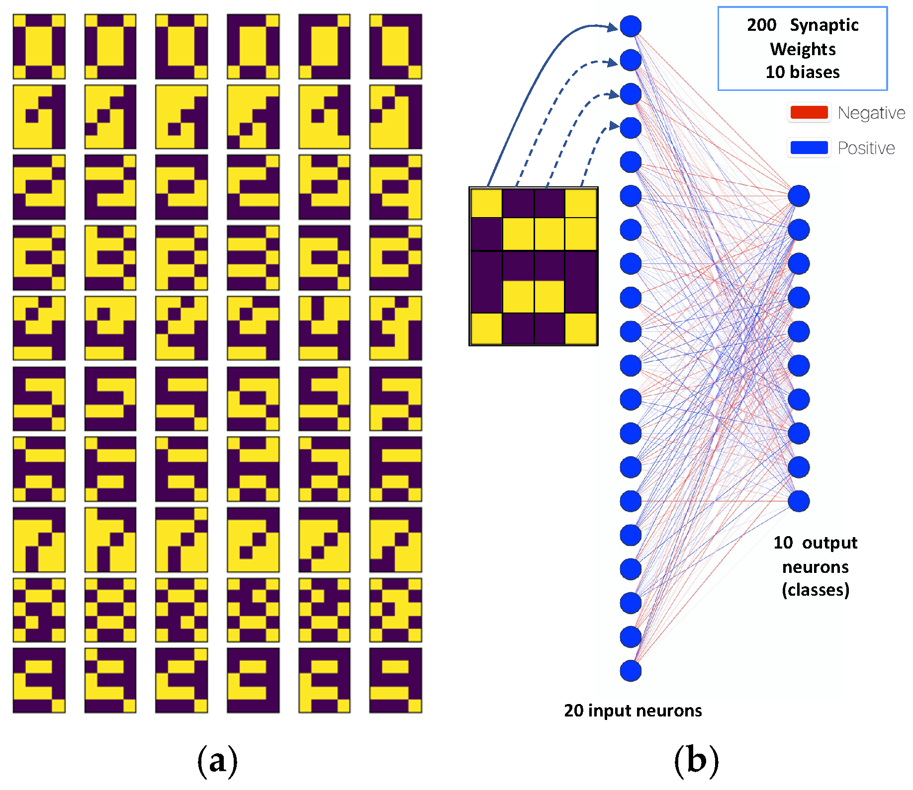
3. Artificial Neural Network Weight Mapping Methodology

In this section, we provide a comprehensive step-by-step overview of implementing an RRAM-based neural network for image classification. The process involves translating the neural network’s parameters, typically weights and biases, from the software domain to an RRAM array. The mapping process consists of three key steps: (i) ANN architecture definition and offline model generation after training using a software-based approach (e.g., Python or MATLAB); (ii) the transfer of the learned weights and biases to the hardware (i.e., RRAM array mapping); and (iii) vector–matrix multiplication execution at the hardware level.

3.1. ANN Architecture Definition and Training

The most studied network architecture in the literature is the fully connected NN [22,23,24,25], where each neuron in a layer is connected to every neuron in the previous layer. In this work, a 2-layer fully connected NN is considered. At the software level, the TensorFlow libraries are used to design and train the 2-layer NN model, along with the custom image dataset presented in Figure 3a. In the context of image classification, an image is represented as a matrix of pixels with the dimensions n × m. We have considered 5 × 4 grayscale images representing digits (0–9), in which the color of the pixels is encoded by one single value: each pixel has a value between 0 (black) and 255 (white). Note that before use, a preprocessing step is needed to convert the images into a format suitable for NN training and inference (pixel values are normalized to a range of 0 to 1). In Figure 3a, each class gathers six different instances of the same digit. Given the small size of the images, a simple feedforward NN with two layers is the target. The input layer is fed 20 inputs encoding the 5 × 4 input pixels. The output layer is made of 10 output neurons and determines the final prediction of the model. The model parameters include 200 synaptic weights and 10 biases. Note that 150 epochs are used to train the model.
In TensorFlow, when generating a neural network (NN) model during training, there are multiple options for setting up the model’s parameters (weights and biases) based on different requirements, including polarity and ranges [25]. A specific case is considered in this study, where the model is generated using only positive weights. This approach simplifies the hardware mapping process, as negative values cannot be represented directly with RRAM cells [26]. This model, providing only positive parameters, is used in the rest of this paper. It has been generated at the software level by setting specific constraints during training.

3.2. Hardware Mapping of the ANN Model Parameters

Figure 4 describes how the neural network model presented in Figure 4a can be mapped to the passive crossbar array shown in Figure 4b. In a passive crossbar array, each cell in the array consists of a single resistive element (1R) at each cross-point. The cells in a row are organized by connecting their top electrodes to input neurons Ix (with x ranging from 1 to 20), while the cells in a column are organized by connecting their bottom electrodes to the output neurons Ox (with x ranging from 1 to 10). However, a common integration option, which is adopted in this study, is to place a CMOS transistor in series with the resistive element to control the current that moves through it using the so-called 1 transistor 1 resistor (1T1R) architecture. This approach prevents current paths through neighboring cells, known as “sneak paths” [27]. These unintended paths lead to leakage currents and reduce the read and write accuracy, as the current contribution of a cell might be influenced by currents from other cells rather than reflecting the target cell’s state.
The parameters of the software model are converted into conductance values during a programming operation that targets individual cells within the crossbar array. This process is facilitated by an additional selection transistor, which enables selective access to each cell and precise control over the current flowing through it, ensuring accurate and reliable conductance mapping. In particular, compliance current control is achieved by adjusting the gate voltage of the selection transistor, allowing the programming of conductance values ranging from 87 μS to 24.7 μS, as detailed in Table 2. Note that the conductance values are derived from the weight matrix using a linear transformation [28]. After conductance mapping, during inference, appropriate input voltages are applied to the crossbar inputs Ix, while all rows are activated through the Word Lines Ox, generating cumulative currents along the columns.

3.3. Vector–Matrix Multiplication in a 1T1R Array

As already mentioned, an array of RRAM cells could naturally accomplish VMM within one step by collecting the output currents of the array. Figure 5b describes how the basic neural network model of Figure 5a can be mapped to a 1T1R crossbar RRAM array.
The cells in a row are organized by attaching the transistor gate nodes to the Source Line (SL) and the transistor drain nodes to the WL, while the cells in a column are arranged by attaching the bottom electrodes of the RRAM cells to the Bit Line (BL). Input vectors (Xx) are associated with input voltages (Vx) and the matrix weights (Wki) are associated with the cell resistance values, Rki. Based on Equation (1), related to Figure 5a, VMM can be easily implemented following Equation (2), related to Figure 5b: when the voltages Vx are applied to the rows, the SLs are turned ON and the current through each cell is proportional to the product of the input voltage and the cell’s conductance (which represents its weight). Accumulation is then performed along the BLs through current summing and reflected in the total current Ik (1 < k ≤ m). Ik currents are considered to be the circuit responses and will be compared with the neural network’s software output to assess the hardware’s emulation accuracy. It is worth mentioning that an activation function (not presented here) can be applied to the total current.
Y k = i = 1 i = n W k i   .   X i    1 < k m
I k = i = 1 i = n 1 R k i   .   V i    1 < k m

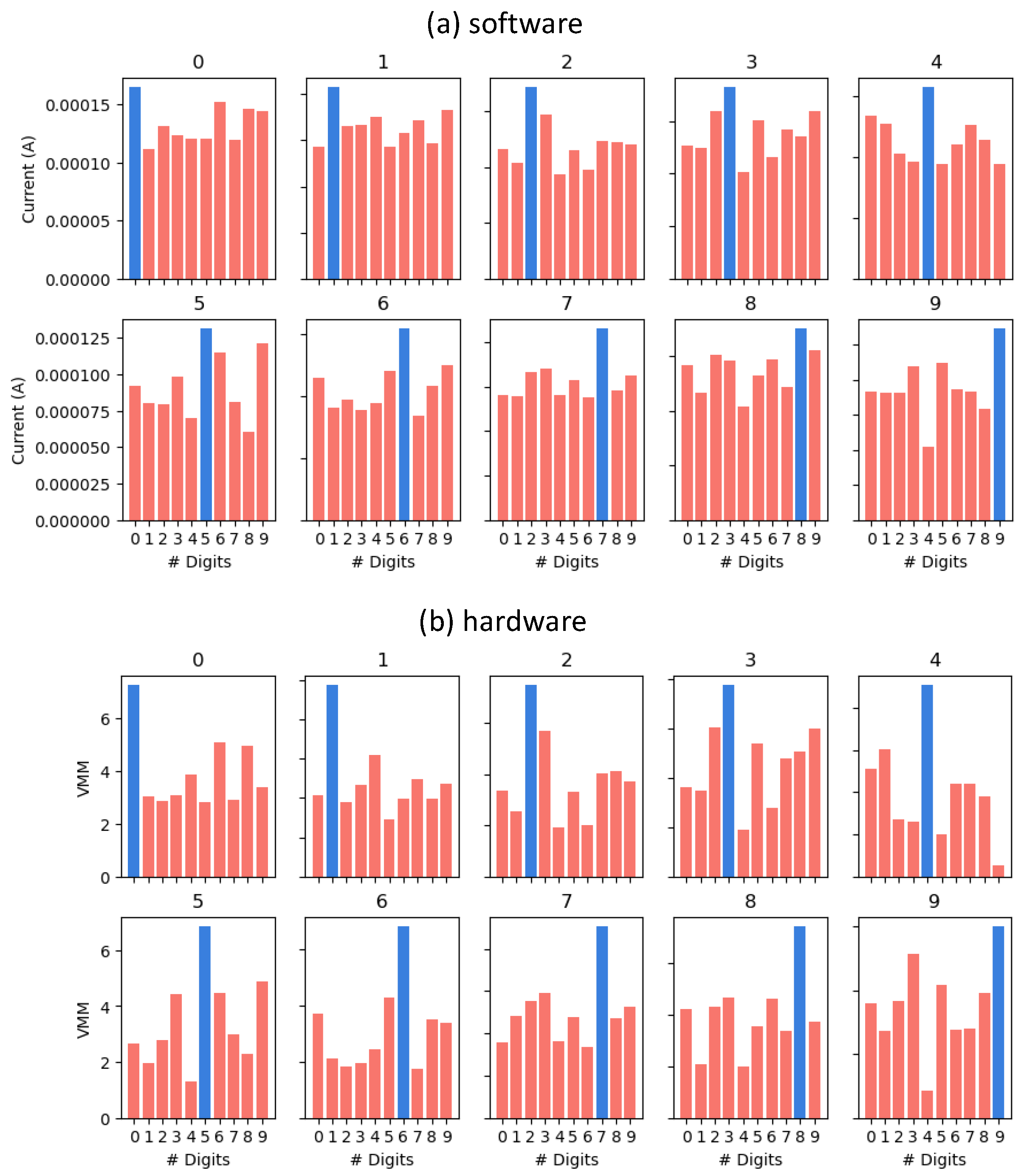
4. Circuit-Level Simulation Results for the Inference Stage

A 20 × 10 1T1R array was designed and simulated using the Eldo simulator within the Cadence environment, using a 0.13 μm high-voltage CMOS technology from ST-Microelectronics. The choice of a high-voltage technology is imposed by the RRAM FMG operation, which requires transistors to sustain a 3.3 V supply voltage. A compact model, fully calibrated on silicon, is used to represent the RRAM cells [29]. The proposed RRAM modeling approach relies on the electric field-induced creation/destruction of oxygen vacancies within the switching layer. The model enables continuous accounting for both SET and RST operations within a single master equation, in which the resistance is controlled by the radius of the conduction filaments (3):
d r C F d t = r CF   max r C F 10 β Re d O x e E a q α r e d V c e l l k b T r C F 10 β Re d O x e E a + q α o x V c e l l k b T
where βRedOx is the nominal oxide reduction rate, Ea is the activation energy, αred and αox are the transfer coefficients (ranging between 0 and 1), kb is the Boltzmann constant, rCFmax is the maximal size of the conductive filament radius, T is the temperature, and Vcell is the voltage across the cell. Moreover, the model makes the assumptions of a uniform radius across the conduction pathways, a uniform electric field in the cell, and a temperature-triggered acceleration of the oxide reduction reactions (“redox”). Finally, the total current in the RRAM array includes two components, i.e., one related to the conductive species, ICF (4), and the other to the conduction through the oxide, IOX (5).
I C F = V C e l l L x π r C F 2 σ C F σ O X + π r C F max 2 σ O X
I O X = A H R S S C e l l V C e l l L x β H R S
where Lx is the oxide’s thickness, SCell is the total area of the device, σOx is the oxidation rate, and σCF is the reduction rate. To take into account the IOX trap-assisted current (Poole-Frenkel, Schottky emission, Space Charge Limited Current (SCLC)), a power law between the cell current and the applied bias is considered, with the two parameters AHRS and βHRS. Finally, the total current flowing through the cell is given in (6):
I C e l l = I C F + I O X
Note that ICF is the main contributor to an LRS current (ILRS) and IOX is the main contributor to an HRS current (IHRS).
Based on this simulation setup, conductance mapping is performed using the compliance current modulation technique to achieve conductance values within the range specified in Table 2. During inference, the digital values of the image pixels are converted to voltage values. A white pixel (255) is associated with a voltage applied to the crossbar rows equal to 0.3 V, while a black pixel (0) is associated with a voltage equal to 0.0 V. These voltages are carefully chosen to ensure no shifting of the RRAM cell conductance state during inference. The model’s accuracy is evaluated based on a new dataset never seen by the model. In this dataset, the color of half of the pixels of each image has been modified to values different from 0 (black) and 255 (white). At the software level, values of 15 and 240 have been chosen for black and white, respectively. At the hardware level, corresponding intermediate voltage values are obtained after a linear transformation.
Figure 6a presents the inference accuracy results obtained through software-based simulations. The X-axis represents the output classes while the Y-axis represents the measured current values. Figure 6b shows the corresponding hardware-based simulation results, where the Y-axis represents the output logits corresponding to the results of the vector–matrix multiplication (VMM) operation, expressed as floating-point values. In classification tasks, logits refer to the raw output (i.e., unnormalized values) produced by the final layer before applying any activation functions, such as softmax.
For each digit ranging from 0 to 9, displayed on the X-axis, blue and red bars represent the amplitudes of the output logits/currents. The blue bar corresponds to the logit/current associated with the target digit (indicated at the top of each histogram), while the red bars correspond to the logits/currents of non-target digits, which should be ignored. For a targeted digit, the inference test is considered successful if the blue bar exceeds all the red bars. Moreover, inference accuracy improves as the margin by which the blue bar surpasses the red bars increases. Based on these observations, Figure 6a,b demonstrate that an overall accuracy of 100% is achieved at both the software and hardware levels. However, the difference between the blue and red bars’ heights is more pronounced in the software results, indicating that classification efficiency is comparatively lower at the hardware level.
To assess the confidence level of the model’s predictions during inference, a parameter called Margin Confidence (MC) [28] can be computed. The MC is defined as the difference between the logits or currents of the most probable class and the second most probable class. A higher MC value indicates a more confident prediction. In this study, the relative average MC of the software approach is 43.82% across all the tested digits, while the hardware approach achieves a relative average MC of 16.39% (a 27.43% drop), highlighting the superior accuracy of the software approach. The drop in classification accuracy at the hardware level is primarily due to the limited conductance range of RRAM technology, which restricts its possible weight values. As shown in Table 2, the mapped weights fall within a conductance range of 87 μS to 24.7 μS. Beyond these intrinsic limitations, circuit-level parasitics, including resistive and capacitive effects from transistors and the RRAM model, also impact the RRAM-based neural network’s accuracy, though to a lesser extent.
From an energy perspective, the hardware simulation results indicate that current levels fall within the range of tens of microamperes, with peak currents reaching 165 μA and an average current consumption during a single inference of 1260.6 μA. The energy efficiency of the inference process can be quantified in various ways, including the total inference energy, which represents the energy required to process an entire input digit. Assuming a 100 ns/0.3 V input voltage pulse during inference (aligned with the RRAM read voltage pulse requirements [25]), the total energy dissipated during inference is found to be 38 pJ. Energy efficiency can also be expressed as the energy consumed per MAC operation, typically expressed in pJ/MAC or fJ/MAC. Given that processing a single input sample involves 200 MAC operations (20 input neurons × 10 output neurons), the energy dissipation per MAC operation is found to be 190 fJ/MAC. Energy-related metrics are summarized in Table 3. Regarding the latency of the VMM engine, it is on the order of nanoseconds, as it is primarily influenced by R-C delays (i.e., resistance–capacitance delays) associated with the crossbar’s interconnections. Since peripheral elements such as DACs and ADCs are not considered in the latency calculation, this parameter should be considered with caution, as currents are generated almost instantaneously at the output of the crossbar array.

5. Discussion

In the adopted software-weighted mapping approach, only positive floating-point numbers were used for the neural network parameters. Implementing negative weights and biases would have required additional rows or columns in the crossbar array, along with increased design complexity [30,31] due to the need for handling additional signals and managing negative voltages. Regarding energy considerations, it is important to note that before inference, memory cells must be programmed to achieve specific conductance levels aligned with the software weight matrix. During this stage, since the RRAM’s write performance is typically orders of magnitude worse than its read performance in terms of energy consumption [32], the NN accelerator needs to be designed to supply this amount of energy. Consequently, to minimize expensive resistive memory programming operations, weights are usually programmed into memory prior to inference and remain fixed throughout the inference process. Regarding the crossbar size, it is important to note that large images typically require a correspondingly large number of rows in the crossbar structure. In software-based ANNs, this is not a challenge. However, the available inputs in hardware NNs are limited by the maximal size of the crossbar. The approach adopted in this study involves generating a set of 5 × 4 custom-designed images, effectively limiting the crossbar to 20 rows. In this work, we have introduced and focused on the analog VMM engine of a hardware accelerator. However, AI accelerators come with unique challenges and limitations related to peripheral circuits, such as ADCs and DACs, which are not addressed here. The accuracy and energy consumption of a VMM engine are often dominated by DACs and ADCs. Depending on DACs’ and ADCs’ architecture, one or several of their performances can grow exponentially with bit precision [33]. Therefore, at high precision, VMM engines may lose the energy and area advantages they have over digital accelerators. Another parameter not addressed in this study is related to the flexibility of the VMM engine, which has been designed in our study to process images of a specific size. For an RRAM chip to be broadly adopted in practical AI applications, not only does it need to deliver notable energy efficiency, but it also needs to offer flexibility to support various AI model architectures [34].
Another challenge to be overcome for reliable RRAM-based VMM engines is related to the variability of the underlying memristor technology. Indeed, RRAM variability poses a significant hurdle for the widespread adoption of RRAM in neuromorphic computing systems. Variability refers to the inherent differences in the electrical characteristics of RRAM devices, even when fabricated under the same manufacturing conditions. This variability can manifest as variations in the key parameters of RRAM devices, including their resistance levels, thus preventing accurate conductance modulation, which is crucial for accurate neural network operations [35]. In addition to variability, over time, a typical bottleneck for OxRAMs lies in their endurance and retention reliability issues. These two reliability metrics narrow the resistance window, thus significantly reducing their conductance modulation capability [36,37]. Note that cycling and endurance can lead to hard errors (such as memory cell being stuck in one state forever). Similarly to other emerging memory technologies, RRAM is inclined to defects [38] due to manufacturing conditions. Hence, appropriate test strategies are required to detect RRAM-related failures [39]. In addition to conventional faults, RRAM, due to its specific manufacturing process and switching mechanism, can be impacted by unique faults such as over-forming and undefined state faults [40]. Therefore, a complete fault analysis methodology needs to be defined for this class of memory technology. Alternatively, RRAM neural networks have the potential to be used in harsh spatial environments [41,42]. In such conditions, there are certain considerations and challenges that need to be addressed for RRAM to operate reliably, such as high levels of radiation, including ionizing particles [43,44]. This radiation can cause unwanted effects, such as resistance drifts, during the OxRAM device’s operation. To mitigate these effects, OxRAM devices need to be radiation-hardened or shielded [9].

6. Conclusions

In recent years, hardware accelerators leveraging emerging resistive memory technologies have shown significant progress. However, research on the ability of resistive devices to efficiently emulate synaptic behavior remains in its early stages. In this context, this study investigates the implementation of RRAM-based crossbar arrays serving as analog VMM (vector–matrix multiplication) engines. Our analysis is supported by experimental data from HfO2-based RRAM devices, whose conductance values can be finely tuned to map the neural network software’s weight matrix. The simulation results demonstrate that both software and hardware implementations of the neural network model achieve 100% inference accuracy. Accuracy results have shown that the classification performance of the hardware is reduced due to the limited conductance range provided by RRAM technology (the relative average MC drops from 43.82% to 16.39%, resulting in a decrease of 27.43%). While the hardware implementation experiences an accuracy degradation, it can achieve significant improvements in power efficiency and computation speed. Hardware simulations have provided an energy consumption of 2.53 pJ/MAC for the VMM engine with a latency on the order of nanoseconds. These results highlight the potential of memristor crossbar arrays as a viable alternative to traditional computing platforms for AI applications, particularly in edge computing scenarios where power constraints are predominant.

Funding

This research received no external funding.

Data Availability Statement

Data are contained within the article.

Conflicts of Interest

The authors declare no conflicts of interest.

References

  1. Linn, E.; Rosezin, R.; Tappertzhofen, S.; Böttger, U.; Waser, R. logic operations in passive crossbar arrays alongside memory operations. Nanotechnology 2012, 23, 305205. [Google Scholar] [CrossRef]
  2. Aitken, R.; Chandra, V.; Myers, J.; Sandhu, B.; Shifren, L.; Yeric, G. Device and technology implications of the Internet of Things. In Symposium on VLSI Technology (VLSI-Technology): Digest of Technical Papers; IEEE: Honolulu, HI, USA, 2014; pp. 1–4. [Google Scholar] [CrossRef]
  3. Aziza, H. Embedded Memories. In Silicon Systems for Wireless Lan; World Scientific: Singapore, 2020; Chapter 7; Volume 22, p. 199. ISBN 978-981-121-071-6. [Google Scholar] [CrossRef]
  4. Indiveri, G.; Linares-Barranco, B.; Legenstein, R.; Deligeorgis, G.; Prodromakis, T.; Tetzlaff, R.; Serrano-Gotarredona, T.; Chicca, E.; Oster, M.; Bartolozzi, C.; et al. Neuromorphic silicon neuron circuits. Front. Neurosci. 2011, 5, 73. [Google Scholar] [CrossRef]
  5. Bi, G.-Q.; Poo, M.-M. Synaptic modifications in cultured hippocampal neurons: Dependence on spike timing, synaptic strength, and postsynaptic cell type. J. Neurosci. 1998, 18, 10464–10472. [Google Scholar] [CrossRef]
  6. Vatajelu, E.I.; Aziza, H.; Zambelli, C. Nonvolatile memories: Present and future challenges. In Proceedings of the Design & Test Symposium (IDT), 2014 9th International, Algeries, Algeria, 16–18 December 2014; IEEE: Piscateville, NJ, USA, 2014; pp. 61–66. [Google Scholar] [CrossRef]
  7. Bazzi, H.; Harb, A.; Aziza, H.; Moreau, M.; Kassem, A. RRAM-based non-volatile SRAM cell architectures for ultra-low-power applications. Analog. Integr. Circuits Signal Process. 2021, 106, 351–361. [Google Scholar] [CrossRef]
  8. Aziza, H.; Moreau, M.; Pérez, A.; Virazel, A.; Girard, P. A capacitor-less CMOS neuron circuit for neuromemristive networks. In Proceedings of the 2019 17th IEEE International New Circuits and Systems Conference (NEWCAS), Munich, Germany, 23–26 June 2019; IEEE: Piscateville, NJ, USA, 2019. [Google Scholar] [CrossRef]
  9. Vaz, P.I.; Girard, P.; Virazel, A.; Aziza, H. Improving TID Radiation Robustness of a CMOS OxRAM-Based Neuron Circuit by Using Enclosed Layout Transistors. In IEEE Transactions on Very Large Scale Integration (VLSI) Systems; IEEE: Piscateville, NJ, USA, 2021; Volume 29, pp. 1122–1131. [Google Scholar] [CrossRef]
  10. Aziza, H.; Bazzi, H.; Postel-Pellerin, J.; Canet, P.; Moreau, M.; Harb, A. An Augmented OxRAM Synapse for Spiking Neural Network (SNN) Circuits. In Proceedings of the 2019 14th International Conference on Design & Technology of Integrated Systems In Nanoscale Era (DTIS), Mykonos, Greece, 16–18 April 2019; pp. 1–5. [Google Scholar] [CrossRef]
  11. Aziza, H.; Zambelli, C.; Hamdioui, S.; Diware, S.; Bishnoi, R.; Gebregiorgis, A. On the Reliability of RRAM-Based Neural Networks. In Proceedings of the IFIP/IEEE 31st International Conference on Very Large Scale Integration (VLSI-SoC), Dubai, United Arab Emirates, 16–18 October 2023; pp. 1–8. [Google Scholar] [CrossRef]
  12. Aziza, H.; Perez, A.; Portal, J.M. Resistive RAMs as analog trimming elements. Solid-State Electron. 2018, 142, 52–55. [Google Scholar] [CrossRef]
  13. Ielmini, D. Resistive switching memories based on metal oxides: Mechanisms, reliability and scaling. Semicond. Sci. Technol. 2016, 31, 063002. [Google Scholar] [CrossRef]
  14. Barlas, M.; Grossi, A.; Grenouillet, L.; Vianello, E.; Nolot, E.; Vaxelaire, N.; Blaise, P.; Traoré, B.; Coignus, J.; Perrin, F.; et al. Improvement of HfO2 based RRAM array performances by local Si implantation. In Proceedings of the 2017 IEEE International Electron Devices Meeting (IEDM), San Francisco, CA, USA, 2–6 December 2017; pp. 14.6.1–14.6.4. [Google Scholar] [CrossRef]
  15. Aziza, H.; Postel-Pellerin, J.; Bazzi, H.; Canet, P.; Moreau, M.; Della Marca, V.; Harb, A. True random number generator integration in a resistive RAM memory array using input current limitation. IEEE Trans. Nanotechnol. 2020, 19, 214–222. [Google Scholar] [CrossRef]
  16. Aziza, H.; Canet, P.; Postel-Pellerin, J.; Moreau, M.; Portal, J.M.; Bocquet, M. ReRAM ON/OFF resistance ratio degradation due to line resistance combined with device variability in 28nm FDSOI technology. In Proceedings of the Joint International EUROSOI Workshop and International Conference on Ultimate Integration on Silicon (EUROSOI-ULIS), Athens, Greece, 3–5 April 2017; IEEE: Piscateville, NJ, USA, 2017. [Google Scholar] [CrossRef]
  17. Aziza, H. Oxide-based Resistive RAM Analog Synaptic Behavior Assessment for Neuromemristive systems. In Memristors—The Fourth Fundamental Circuit Element—Theory, Device, and Applications; IntechOpen: London, UK, 2023. [Google Scholar] [CrossRef]
  18. Aziza, H.; Hamdioui, S.; Fieback, M.; Taouil, M.; Moreau, M. Density Enhancement of RRAMs using a RESET Write Termination for MLC Operation. In Proceedings of the Design, Automation 459 & Test in Europe Conference & Exhibition (DATE), Grenoble, France, 1–5 February 2021; pp. 1877–1880. [Google Scholar] [CrossRef]
  19. Kim, W.; Menzel, S.; Wouters, D.J.; Waser, R.; Rana, V. 3-Bit multilevel switching by deep reset phenomenon in Pt/W/TaOx /Pt-ReRAM devices. IEEE Electron. Device Lett. 2016, 37, 564–567. [Google Scholar] [CrossRef]
  20. Aziza, H.; Postel-Pellerin, J.; Moreau, M. STATE: A Test Structure for Rapid and Reliable Prediction of Resistive RAM Endurance. IEEE Trans. Device Mater. Reliab. 2022, 22, 500–505. [Google Scholar] [CrossRef]
  21. Zhao, L.; Chen, H.Y.; Wu, S.C.; Jiang, Z.; Yu, S.; Hou, T.H.; Philip Wong, H.-S.; Nishi, Y. Improved multi-level control of RRAM using pulse-train programming. In Proceedings of the IEEE International Symposium on VLSI Technology, Systems and Application (VLSI-TSA), Hsinchu, Taiwan, 28–30 April 2014. [Google Scholar] [CrossRef]
  22. Papandroulidakis, G. Experimental Demonstration of RRAM-Based Computational Cells for Reconfigurable Mixed-Signal Neuro-Inspired Circuits and Systems. Ph.D. Dissertation, University of Southampton, Southampton, UK, 2021. [Google Scholar]
  23. Lee, Y.-L.; Tsung, P.-K.; Wu, M. Technology trend of edge AI. In Proceedings of the Symposium on VLSI Design, Automation and Test (VLSI-DAT), Hsinchu, Taiwan, 16–19 April 2018; pp. 1–2. [CrossRef]
  24. Aziza, H.; Postel-Pellerin, J.; Fieback, M.; Hamdioui, S.; Xun, H.; Taouil, M.; Coulié, K.; Rahajandraibe, W. Analysis of Conductance Variability in RRAM for Accurate Neuromorphic Computing. In Proceedings of the 2024 IEEE 25th Latin American Test Symposium (LATS), Maceio, Brazil, 9–12 April 2024; pp. 1–5. [Google Scholar] [CrossRef]
  25. Portal, J.M.; Bocquet, M.; Onkaraiah, S.; Moreau, M.; Aziza, H.; Deleruyelle, D.; Kholdoun, T.; Vianello, E.; Levisse, A.; Bastien, G.; et al. Design and simulation of a 128 kb embedded nonvolatile memory based on a hybrid RRAM (HfO2)/28 nm FDSOI CMOS technology. IEEE Trans. Nanotechnol. 2017, 16, 677–686. [Google Scholar] [CrossRef]
  26. Aguirre, F.; Sebastian, A.; Le Gallo, M.; Song, W.; Wang, T.; Yang, J.J.; Lu, W.; Chang, M.-F.; Ielmini, D.; Yang, Y.; et al. Hardware implementation of memristor-based artificial neural networks. Nat. Commun. 2024, 15, 1974. [Google Scholar] [CrossRef]
  27. Zidan, M.A.; Fahmy, H.A.H.; Hussain, M.M.; Salama, K.N. Memristor-based memory: The sneak paths problem and solutions. Microelectron. J. 2013, 44, 176–183. [Google Scholar] [CrossRef]
  28. Hu, M.; Strachan, J.P.; Li, Z.; Grafals, E.M.; Davila, N.; Graves, C.; Lam, S.; Ge, N.; Yang, J.J.; Stanley Williams, R. Dot-product engine for neuromorphic computing. In Proceedings of the DAC’16: Proceedings of the 53rd Annual Design Automation Conference, Austin, TX, USA, 5–9 June 2016; Association for Computing Machinery: New York, NY, USA, 2016; pp. 1–6. [Google Scholar] [CrossRef]
  29. Hajri, B.; Mansour, M.M.; Chehab, A.; Aziza, H. Oxide-based RRAM models for circuit designers: A comparative analysis. In Proceedings of the International Conference on Design & Technology of Integrated Systems In Nanoscale Era (DTIS), Palma de Mallorca, Spain, 4–6 April 2017. [Google Scholar] [CrossRef]
  30. Aziza, H.; Fieback, M.; Hamdioui, S.; Xun, H.; Taouil, M. Conductance variability in RRAM and its implications at the neural network level. Microelectron. Reliab. 2025, 166, 115594. [Google Scholar] [CrossRef]
  31. Yuan, G.; Ma, X.; Ding, C.; Lin, S.; Zhang, T.; Jalali, Z.S.; Zhao, Y.; Li, J.; Soundarajan, S.; Wang, Y. An Ultra-Efficient Memristor-Based DNN Framework with Structured Weight Pruning and Quantization Using ADMM. arXiv 2019, arXiv:1908.11691. [Google Scholar] [CrossRef]
  32. Aziza, H.; Moreau, M.; Fieback, M.; Taouil, M.; Hamdioui, S. An Energy-Efficient Current-Controlled Write and Read Scheme for Resistive RAMs (RRAMs). IEEE Access 2020, 8, 137263–137274. [Google Scholar] [CrossRef]
  33. Xiao, T.P.; Bennett, C.H.; Feinberg, B.; Agarwal, S.; Marinella, M.J. Analog architectures for neural network acceleration based on non-volatile memory. Appl. Phys. Rev. 2020, 7, 031301. [Google Scholar] [CrossRef]
  34. Cho, S.M.; Yoon, R.; Yoon, I.; Moon, J.; Oh, S.; Min, K.S. Optimization of Memristor Crossbar’s Mapping Using Lagrange Multiplier Method and Genetic Algorithm for Reducing Crossbar’s Area and Delay Time. Information 2024, 15, 409. [Google Scholar] [CrossRef]
  35. Postel-Pellerin, J.; Bazzi, H.; Aziza, H.; Canet, P.; Moreau, M.; Della Marca, V.; Harb, A. True random number generation exploiting SET voltage variability in resistive RAM memory arrays. In Proceedings of the 2019 19th Non-Volatile Memory Technology Symposium (NVMTS), Durham, NC, USA, 28–30 October 2019; pp. 1–5. [Google Scholar] [CrossRef]
  36. Lanza, M.; Waser, R.; Ielmini, D.; Yang, J.J.; Goux, L.; Suñe, J.; Kenyon, A.J.; Mehonic, A.; Spiga, S.; Rana, V.; et al. Standards for the Characterization of Endurance in Resistive Switching Devices. ACS Nano 2021, 15, 17214–17231. [Google Scholar] [CrossRef]
  37. Rana, A.M.; Akbar, T.; Ismail, M.; Ahmad, E.; Hussain, F.; Talib, I.; Imran, M.; Mehmood, K.; Khalid, I.; Nadeem, M.Y. Endurance and Cycle-to-Cycle Uniformity Improvement in Tri-Layered CeO2/Ti/CeO2 Resistive Switching Devices by Changing Top Electrode Material. Sci. Rep. 2017, 7, 39539. [Google Scholar] [CrossRef] [PubMed]
  38. Fieback, M.; Medeiros, G.C.; Wu, L.; Aziza, H.; Bishnoi, R.; Taouil, M.; Hamdioui, S. Defects, fault modeling, and test development framework for RRAMs. ACM J. Emerg. Technol. Comput. Syst. (JETC) 2022, 18, 1–26. [Google Scholar] [CrossRef]
  39. Fieback, M.; Wu, L.; Medeiros, G.C.; Aziza, H.; Rao, S.; Marinissen, E.J.; Taouil, M.; Hamdioui, S. Device-Aware Test: A New Test Approach Towards DPPB Level. In Proceedings of the IEEE International Test Conference (ITC), Washington, DC, USA, 9–15 November 2019; pp. 1–10. [Google Scholar] [CrossRef]
  40. Fieback, M.; Medeiros, G.C.; Gebregiorgis, A.; Aziza, H.; Taouil, M.; Hamdioui, S. Intermittent undefined state fault in RRAMs. In Proceedings of the 2021 IEEE European Test Symposium (ETS), Bruges, Belgium, 24–28 May 2021; IEEE: Piscateville, NJ, USA, 2021; pp. 1–6. [Google Scholar]
  41. Castellani-Coulie, K.; Toure, G.; Portal, J.M.; Ginez, O.; Aziza, H.; Lesea, A. Circuit effect on collection mechanisms involved in single event phenomena: Application to the response of a NMOS transistor in a 90 nm SRAM cell. IEEE Trans. Nucl. Sci. 2011, 58, 870–876. [Google Scholar] [CrossRef]
  42. Castellani-Coulié, K.; Aziza, H.; Rahajandraibe, W.; Micolau, G.; Portal, J.M. Development of a CMOS Oscillator Concept for Particle Detection and Tracking. IEEE Trans. Nucl. Sci. 2013, 60, 2450–2455. [Google Scholar] [CrossRef]
  43. Coulié, K.; Aziza, H.; Rahajandraibe, W. Investigation of Single Event Effects in a Resistive RAM Memory Array by Coupling TCAD and SPICE Simulations. J. Electron. Test 2023, 39, 275–288. [Google Scholar] [CrossRef]
  44. Castellani-Coulié, K.; Bocquet, M.; Aziza, H.; Portal, J.M.; Rahajandraibe, W.; Muller, C. SPICE level analysis of Single Event Effects in an OxRRAM cell. In Proceedings of the 2013 14th Latin American Test Workshop-LATW, Cordoba, Argentina, 3–5 April 2013; pp. 1–5. [Google Scholar] [CrossRef]
Figure 1. (a) Symbol of a 1T1R cell. (b) SEM cross-section of the RRAM stack [14]. (c) RRAM I-V hysteresis.
Electronics 14 01125 g001
Figure 2. (a) Different OxRAM I-V hysteresis in the SET direction for increasing VWL voltage values and (b) RLRS (VWL) for different VWL values. The VWL ranges from 1 V to 2 V with a 0.1 V voltage step.
Electronics 14 01125 g002
Figure 3. (a) 5 × 4 grayscale patterns representing digits (0–9). Each class contains six different instances of the same digit. (b) Two-layer fully connected neural network made of 20 input neurons and 10 output neurons. The network is defined by 210 parameters (200 weights and 10 biases).
Electronics 14 01125 g003
Figure 4. (a) Two-layer fully connected NN featuring 20 inputs and 10 outputs and (b) this neural network mapped to a crossbar array.
Electronics 14 01125 g004
Figure 5. (a) Basic two-layer feed-forward NN model and (b) that NN mapped to a 1T1R crossbar RRAM array.
Electronics 14 01125 g005
Figure 6. Inference accuracy results obtained at the (a) software and (b) hardware level. Blue and red bars represent the amplitudes of the output logits/currents. The blue bar corresponds to the logit/current associated with the target digit (indicated at the top of each histogram).
Electronics 14 01125 g006
Table 1. Standard RRAM cell operating voltages.
FMGRSTSETREAD
WL2 V2.5 V2 V2.5 V
BL3.3 V0 V1.2 V0.1 V
SL0 V1.2 V0 V0 V
Resistance10 kΩ240 kΩ15 kΩ-
Conductance100 μS4.17 μS66.6 μS-
Table 2. OxRAM conductance modulation range.
ParameterMinMax
VWL1 V1.8 V
Resistance11.5 kΩ40.4 kΩ
Conductance87 μS24.7 μS
Table 3. Neural network energy efficiency during inference.
Inference ParametersValue
Crossbar current12,686 μA
Crossbar power37.8 mW
Total inference energy38 pJ
Energy/MAC190 fJ/MAC
Disclaimer/Publisher’s Note: The statements, opinions and data contained in all publications are solely those of the individual author(s) and contributor(s) and not of MDPI and/or the editor(s). MDPI and/or the editor(s) disclaim responsibility for any injury to people or property resulting from any ideas, methods, instructions or products referred to in the content.

