Article

Development of a Three-Phase Universal Programmable Electronic Load (UPEL) Using Adaptive Sliding Pulse Width Modulation (ASPWM) for Enhanced Power Electronics Performance

by
José R. Ortiz-Castrillón
1,2,3,
Sergio D. Saldarriaga-Zuluaga
3,
Nicolás Muñoz-Galeano
1,
Jesús M. López-Lezama
1,* and
Santiago Benavides-Córdoba
1
1
Research Group on Efficient Energy Management (GIMEL), Department of Electrical Engineering, Universidad de Antioquia (UdeA), Medellín 050010, Colombia
2
Department of Electronics and Telecommunications Engineering, Universidad de Antioquia (UdeA), Medellín 050010, Colombia
3
Departamento de Eléctrica, Facultad de Ingeniería, Institución Universitaria Pascual Bravo, Calle 73 No. 73A-226, Medellín 050036, Colombia
*
Author to whom correspondence should be addressed.
Electronics 2025, 14(6), 1100; https://doi.org/10.3390/electronics14061100
Submission received: 23 January 2025 / Revised: 5 March 2025 / Accepted: 8 March 2025 / Published: 11 March 2025

Abstract

:
This paper presents the development of a Three-phase Universal Programmable Electronic Load (UPEL) programmed as an unbalanced and distorted current source, highlighting its innovative control strategy and modulation approach. The core contribution is the implementation of Adaptive Sliding Pulse Width Modulation (ASPWM), a novel technique that combines Sliding Mode Control (SMC) with an Adaptive Hysteresis Band (AHB). This methodology eliminates the need for conventional Pulse Width Modulation (PWM), hybrid PI controllers, or cascade control structures, achieving superior robustness, faster response times, and a fixed switching frequency. The proposed ASPWM enhances energy quality by enabling precise control of active and reactive power, harmonic injection, and operation across multiple modes, including AC/DC rectification and DC/AC inversion. Simulation and experimental results validate the effectiveness of ASPWM in improving performance metrics, ensuring operational stability, and demonstrating adaptability for diverse scenarios. This study establishes ASPWM as a transformative control technique for advanced power electronics applications.

1. Introduction

Simulation and emulation of equipment with power electronics devices such as Programmable Electronic Loads (PELs) are important to ensure correct behavior for the testing of power systems [1]. Simulation provides design criteria for making decisions regarding the sizing, operation, and limitations of equipment, while emulation with Programmable Electronic Loads allows operational testing of equipment before and after connecting power devices to power systems [2,3]. Generally, a PEL is built to emulate load or source profiles in two ways: (1) As a load, a PEL is connected to different generation sources, for example, a photovoltaic system (solar panel, converter/inverter, and batteries) to evaluate parameters in generation, control, storage, efficiency, stability, etc. (2) As a source, the PEL operates as a variable, regulated, protected, and controlled electrical source, where, it is possible to feed a load with different electrical signals (AC or DC) monitoring under safe operation conditions [2].
The most common use of PELs consists of operating (dissipate or regenerate energy to the electrical grid [4]) DC [5,6,7], AC single-phase, and three-phase waveforms as linear and nonlinear loads in MGs [8,9], emulating resistive, resistive-inductive, and resistive-capacitive profiles, such as motors [8], transformers with harmonics [3], and rectifiers [9]. In general, PELs have great flexibility for a wide range of industrial and renewable energy applications; however, a PEL is designed to meet limited functions for a specific test based on the three-phase inverter topology.
The most common topology for building PELs is the three-phase inverter because it allows the emulation of single-phase and three-phase electrical profiles [3,10,11]. In the same way, PI control together with PWM or SPWM (according to application) modulations are the most common methods to switch PELs and obtain load or source profiles [6,10,11,12,13]. PI controls are limited by a system operation point, since, their design and PWM or SPWM modulators contribute to reducing the system response when a control action is sent to power switches. However, nonlinear control strategies provide better behavior, robustness, and faster response than classical PI controls [14].
SMC is a nonlinear control technique based on on–off action, closed and open switches (in this case) [15,16]. This control provides an instantaneous response only limited by the measurement process and microcontroller processing time; therefore, it is common to implement systems with SMC with added PI control and PWM modulators. These hybrid controllers increase PI behavior, penalizing the SMC response, and limiting the system to the PI controller velocity. Such a limitation is performed to avoid damages to power electronics devices due to an uncontrolled switching frequency from the implementation of SMC [17,18,19].
Additionally, traditional modulation techniques, such as Sinusoidal Pulse Width Modulation (SPWM), Space Vector Modulation (SVM), and Hysteresis-Based Sliding Mode Control (HBSMC), each have inherent advantages and limitations in power electronics applications. SPWM is widely used due to its simplicity and fixed switching frequency [20]. However, it suffers from moderate Total Harmonic Distortion (THD), slower dynamic response, and limited adaptability to nonlinear loads. In contrast, SVM improves THD and power factor performance but requires complex mathematical calculations involving sector determination and coordinate transformations, making its real-time implementation computationally demanding [21]. HBSMC, on the other hand, provides fast response times and robustness to parameter variations, making it effective for real-time applications. However, its variable switching frequency leads to increased THD, making filter design more challenging and increasing power losses. Furthermore, hysteresis control lacks precise harmonic injection capabilities, limiting its effectiveness in applications that require power quality enhancement [22].
This paper extends the research presented in [23,24,25], where a Sliding Mode Control (SMC) with an Adaptive Hysteresis Band (AHB) was implemented in a semi-bridgeless boost converter (AC/DC rectifier). The previous work focused on achieving stability and controlling voltage and current simultaneously while limiting the switching frequency, without compromising the SMC’s inherent response speed and robustness. Building on this foundation, the present study advances the methodology by applying the same sliding-surface approach to a single-phase Power PEL and rigorously validating its stability under sliding-mode conditions. Furthermore, this paper extends the scope to three-phase AC/DC rectification and DC/AC inversion, incorporating energy quality functions to enhance the system’s robustness and precision. The proposed approach demonstrates superior performance and maintains high operational accuracy in various operating modes, ensuring reliable energy conversion in various scenarios.
The proposed ASPWM technique combines the benefits of Sliding Mode Control with an Adaptive Hysteresis Band, ensuring a fixed switching frequency while maintaining fast transient response and low THD. Unlike SPWM, ASPWM provides superior adaptability to nonlinear and unbalanced loads. Compared with SVM, ASPWM achieves similar power quality improvements with lower computational complexity, making it more suitable for real-time applications with constrained processing power. Additionally, ASPWM enables active power factor control and harmonic injection, making it a promising alternative for active power filtering, smart grid integration, and adaptive power management systems, as is shown in Table 1.
The implementation of three-phase UPEL is carried out following the procedure presented in [24] as follows: (1) The introduction (Section 1) presents a brief summary of the research work in PELs and SMC, as well as the main research work on which this paper is based. (2) In Section 2, the UPEL topology, the sliding surface, and the AHB are presented in a general form. (3) Section 3 presents the mathematical procedure and validations for UPEL operation as a three-phase rectifier. (4) Section 4 presents the mathematical procedure and validations for UPEL operation as a three-phase inverter. (5) Section 5 presents an additional contribution of this paper: the mathematical procedure and validations for the UPEL operation as a distorted controlled current source. (6) Section 6 presents the correct behavior of the UPEL with the proposed modulation for each operation mode using simulation results. (7) In Section 7, the main experimental results are presented and analyzed to validate the proposed control in a real environment. (8) Finally, the most relevant conclusions are presented in Section 8.

2. General Presentation of the Topology and Control

This section provides a comprehensive overview of the implemented topology and the control strategy used to operate the UPEL. The main topology consists of a three-phase inverter with three branches and four wires, whose operation varies according to the specific operating mode. While the SMC remains consistent across all modes, the control logic adapts to accommodate the requirements of each operational scenario. The primary objective is to show that the proposed modulation strategy is versatile and effective for both three-phase AC/DC rectifiers and DC/AC inverters.

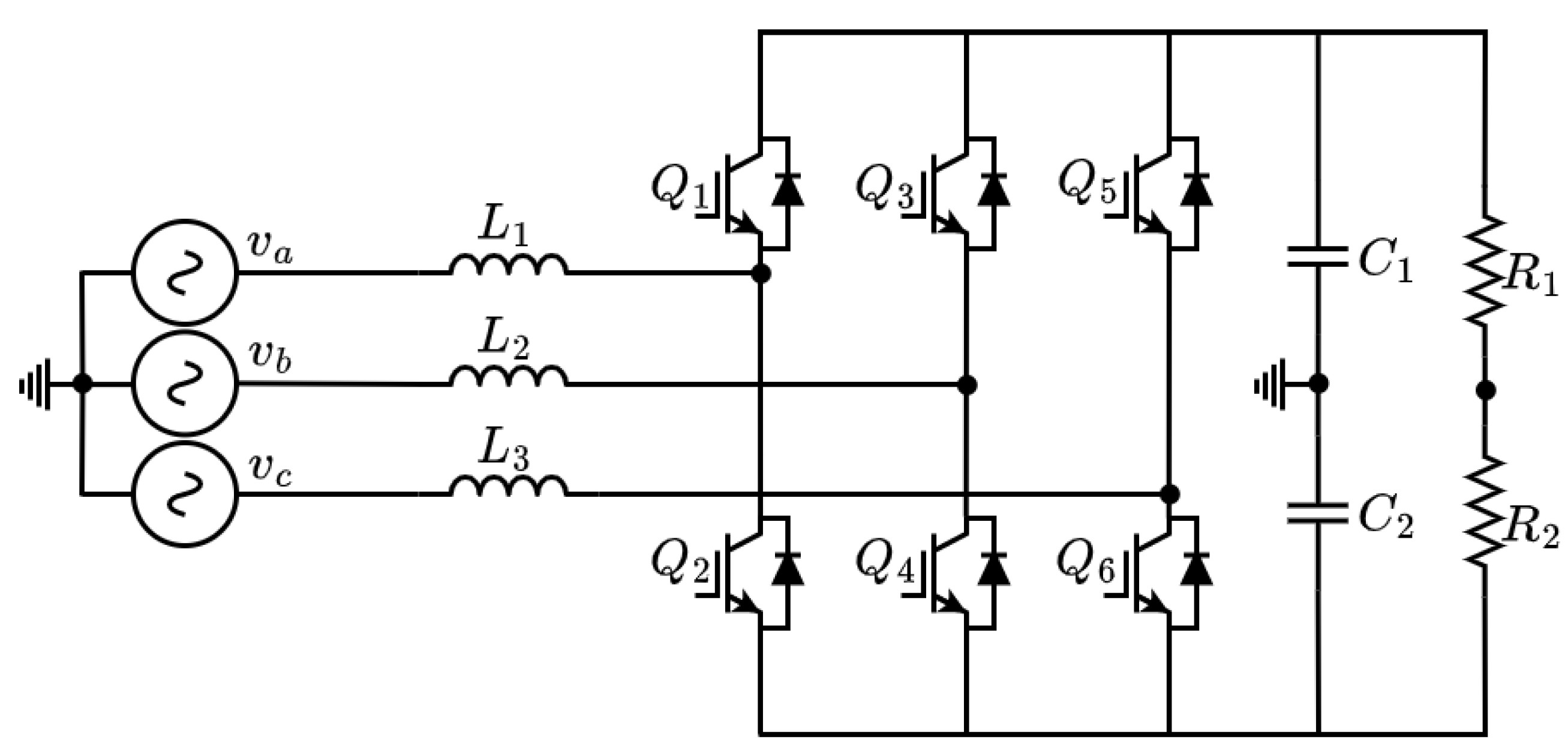
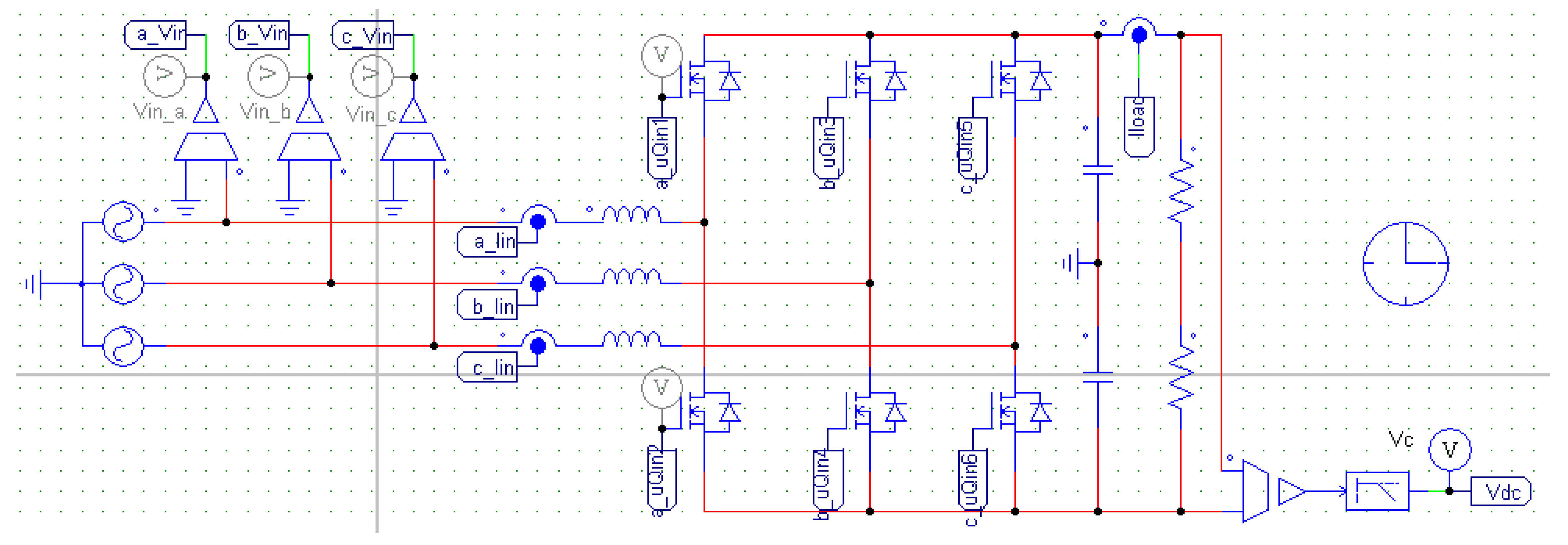
2.1. Three-Phase Inverter Topology: Three Branches, Four Wires

Figure 1 illustrates the base topology of the UPEL implemented in this study. The topology consists of the following. Three inductors L 1 = L 2 = L 3 = L , which act as filters and enable precise current control. Six power switches Q 1 , Q 2 , Q 3 , Q 4 , Q 5 , and Q 6 , responsible for managing the power flow. A split DC bus with two capacitors, C 1 = C 2 = C , facilitates DC voltage control and allows the creation of a neutral point. Two resistive loads R 1 = R 2 = R .
The topology accommodates various feeding sources and adapts the operation of switches and control logic based on each UPEL operating mode. This configuration was chosen for its versatility, as it can function as both a single-phase and a three-phase bidirectional inverter, depending on the control strategy. Although the inverter can be powered by three-phase sources (e.g., v a , v b , v c ), single-phase sources, or DC sources, this paper focuses on equivalent sources tailored to the specific operating function. This approach highlights the applicability of the same Adaptive Sinusoidal Pulse Width Modulation (ASPWM) across all cases, simplifying the mathematical analysis while maintaining consistent performance.

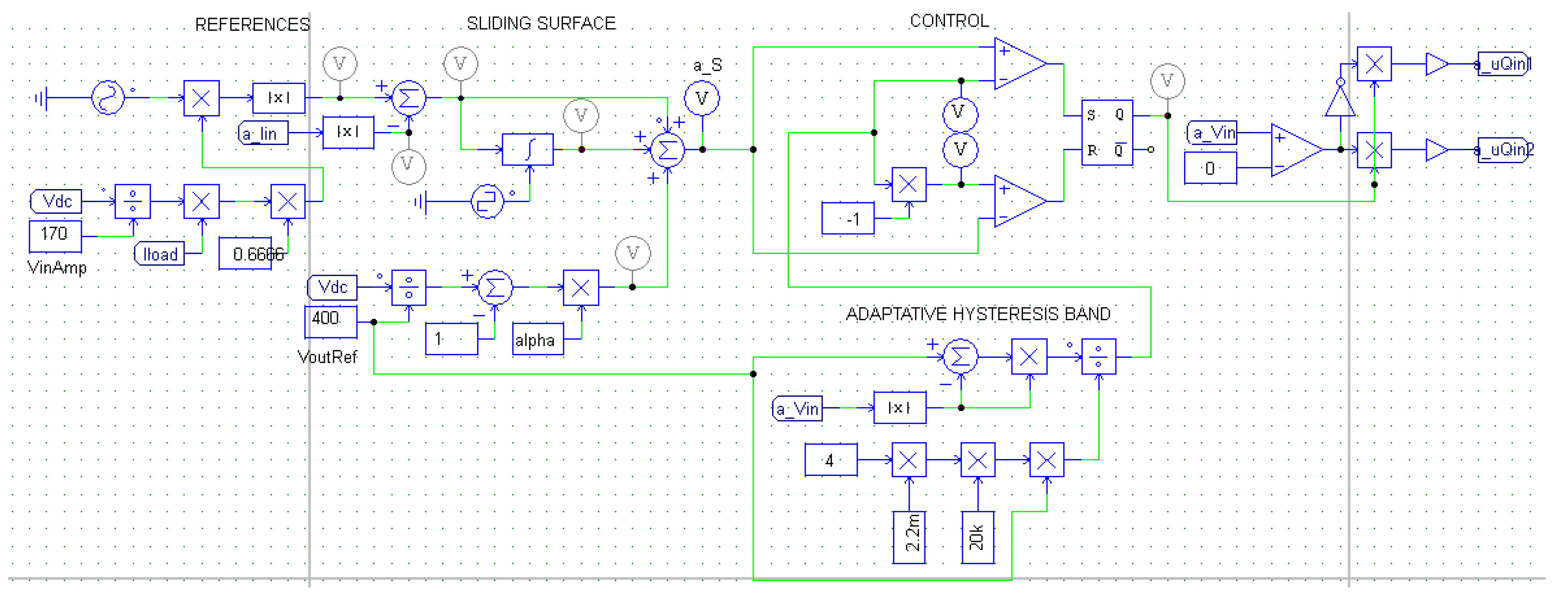
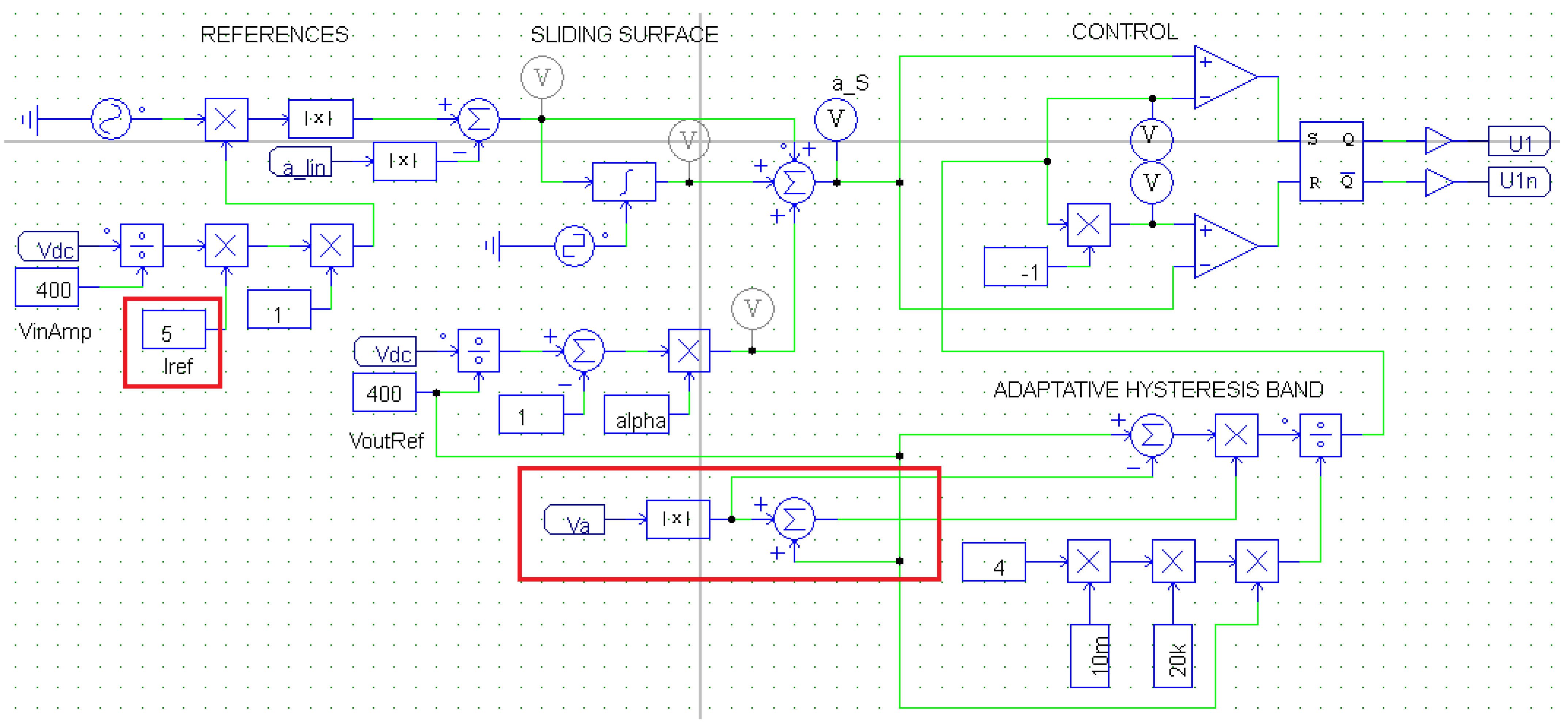
2.2. Adaptive Sliding Pulse Width Modulation

This paper introduces a novel control method, Adaptive Sliding Pulse Width Modulation (ASPWM), designed for simultaneous voltage and current control in AC/DC and DC/AC power converters. The proposed approach ensures high energy quality, adhering to international standards such as IEC 61000-3-2 [26], IEEE 519 [27], and IEEE guidelines. A key contribution of this work is the comprehensive validation of the ASPWM methodology for three-phase converters, where the Adaptive Hysteresis Band (AHB) is dynamically calculated based on the current ripple in the small-signal model. Unlike traditional SMC implementations, which often suffer from variable switching frequencies and require additional hybrid controls or PWM modulators to stabilize the system, the proposed ASPWM method achieves a fixed switching frequency without compromising control performance or requiring auxiliary mechanisms [23,24,25]. This paper demonstrates the robustness, precision, and applicability of the ASPWM method in various operating modes, highlighting its potential for reliable energy conversion with enhanced performance.
The ASPWM operates through two key steps: (1) Sliding Mode Control (SMC): this involves defining the sliding surface and ensuring stability conditions are satisfied based on Lyapunov’s criteria. (2) Adaptive Hysteresis Band (AHB): this represents the bandwidth of the sliding surface, which is dynamically determined by using the current ripple.

2.2.1. Sliding Surface

Equation (1) presents the sliding surface (S) used to control all topologies analyzed in this paper [24]. In this case, the sliding surface can be selected, changed or modified according to designer’s criteria, so the sliding surface is designed according to the variables to be controlled. The main function of the sliding surface is the control of current and DC bus voltage; then, the main objective of the control consists on minimizing three components: (1) the normalized voltage error S 1 between the DC bus voltage ( v o ) and the reference voltage ( V r e f ). This component avoids the nonminimum behavior in Boost topologies. (2) The current error S 2 between the input current ( i s ) and its reference ( i r e f ). (3) The integral of S 2 used to increase the robustness of the control at start-up. In this case, α 1 , α 2 and α 3 represent the sliding coefficients.
S = α 1 v o V r e f 1 S 1 α 2 ( i s i r e f ) S 2 α 3 ( i s i r e f ) d t S 3

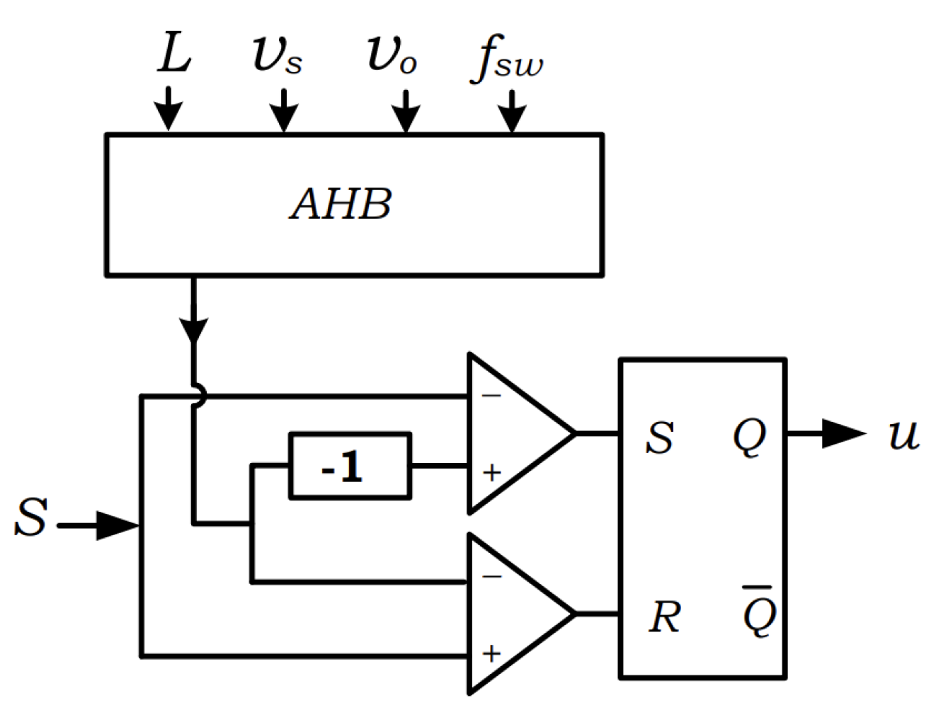
2.2.2. Adaptive Hysteresis Band

Figure 2 [23] presents the general scheme for the implementation of the AHB. The shape of the AHB is determined by the input voltage ( v s ) AC or DC, f s w is the desired switching frequency, L is the inductor obtained from the converter design. The AHB is the limit of variation in the ripple in current or voltage; then, in Figure 2, S it is compared with the AHB by a flip-flop RS to obtain a control signal u to the remaining S in the AHB.

3. UPEL Operation as AC/DC Rectifier

This section establishes the operation principles of the UPEL as AC/DC rectifier. Figure 1 is the starting point. In this configuration, inductors are defined as L 1 = L 2 = L / 2 , with currents i a , i b , and i c flowing through them; the loads are R 1 = R 2 = R / 2 ; and the capacitors are C 1 = C 2 = C , resulting in an output voltage V D C = v C 1 + v C 2 . The control signal u determines the state of the switch, where u = 1 indicates a closed switch and u = 0 an open switch.

3.1. Operating Principle

Figure 3 illustrates the UPEL operating as a rectifier with a three-phase feed source ( v a , v b , and v c ). Equations can be derived in two ways: (1) without a neutral line in the DC bus, using line-to-line voltages and currents, and (2) with a neutral line in the DC bus, using neutral-line voltages and currents. Both approaches result in a circuit similar to the Boost converter per phase, operating independently with a phase shift of 120 , as typical in three-phase systems. The equivalent Equations (2) and (3) can be obtained for each phase.
Two cases must be considered:
(1) Positive Half-Cycle: As shown in Figure 3a, switches Q 1 , Q 3 , and Q 5 are open, while switching occurs in Q 2 , Q 4 , and Q 6 . In this cycle, the system behaves as three independent Boost converters.
(2) Negative Half-Cycle: As depicted in Figure 3b, switches Q 2 , Q 4 , and Q 6 are open, with switching performed in Q 1 , Q 3 , and Q 5 . In this cycle, the system operates as another set of three Boost converters, using inverse logic.
d v R d t = v R R C + ( 1 u ) i a , b , c C
d i a , b , c d t = v a , b , c L ( 1 u ) v R L

3.2. Adaptive Hysteresis Band

The derivation of Equation (4) for the AHB shown in Figure 2, for a semi-bridgeless Boost Converter with clamped diodes is available in [23,24]. This equation applies to all UPEL operating modes described in this section, as both single-phase and three-phase operations consist of independent Boost converters governed by the same mathematical model.
The AHB is derived on the basis of the current ripple and adapts to the form of the power supply. If the input voltage v s is AC, the AHB assumes a sinusoidal shape. Conversely, if v s has a triangular waveform, the AHB will also exhibit a triangular shape. The reference DC bus voltage, v C r e f , is used to ensure that the band maintains a constant maximum amplitude. Furthermore, in the case of a three-phase source, v s = v a , b , c , the AHB is calculated independently for each phase, ensuring proper operation in all phases.
A H B = | v s | ( v C r e f | v s | ) 2 L f s w v C r e f

4. UPEL Operation as Three-Phase DC/AC Inverter

This section presents the operation of the UPEL as a single-phase DC/AC inverter and a three-phase inverter, taking as a starting point the topology of Figure 1.

4.1. Operating Principle

The UPEL topology for the operation of the inverter is depicted in Figure 4. Compared with the configuration in Figure 1, the primary difference lies in the swapped positions of the source and the load. This design corresponds to the conventional three-phase inverter topology with a split DC bus. Its mathematical modeling given by Equations (5) and (6) is consistent across all phases, similar to a single-phase inverter, while accounting for the standard 120 phase shift between phases.
d v c d t = ( 1 2 u ) C i a , b , c
d i a d t = v a , b , c L + ( 1 2 u ) L v c

4.2. Adaptive Hysteresis Band

Equation (7) corresponds to the AHB of both single-phase and three-phase inverters. This equation was derived following the procedure presented in [23]. The AHB is deduced by analyzing the current ripple, considering three important arguments: (1) Constant DC Bus Voltage ( V D C ): V D C is assumed to be constant (DC bus stable). If the designer aims to control the DC bus, then V D C should be equal to V C r e f . (2) For DC/AC operation, V D C is equal to twice the capacitor voltage, 2 v C . (3) If the source is three-phase, then v s corresponds to v a , b , c , requiring an AHB for each phase (independent operation). In this case, f s w corresponds to the switching frequency. This methodology for the AHB in both single-phase and three-phase inverters is an additional contribution of this paper.
A H B = ( V D C + | v s | ) ( V D C | v s | ) 4 L f s w V D C

4.3. SMC Validation

This subsection is another contribution of this work. It presents the sliding conditions and control logic for the UPEL operation as an inverter for the sliding surface presented in Equation (1). The procedure is the same as presented in [24], with the following consideration: the control reference for the converter input is a rectifier signal (as shown in Equation (7)), in order to avoid system instabilities in the negative half-cycle of the feeding source. This means that the reference signals have the same form for the UPEL operation as both the rectifier and the inverter. Therefore, the reference for the UPEL current is given by Equation (8), with I r e f being its amplitude when the inverter is single-phase, while the amplitude is I r e f / 3 if it operates as a three-phase inverter.
i r e f = 2 V r e f 2 R V s I r e f | s i n ( w t ) |
The stability conditions based on the Lyapunov theorem are fulfilled according to the following equations:
  • Transversality Condition: This evaluates if the inverter can be controlled using the control signal u according to Equation (9). This condition is fulfilled considering Equation (10) obtained to solve Equation (9) with Equations (1), (5) and (6), and evaluating in the system limits according to v s . The right side of Equation (10) is multiplied by 3 if the inverter is three-phase; nevertheless, operation as single-phase (Equation (10)) is more restrictive; therefore, this paper works with this restriction.
    d d u d S d t 0
    α 1 α 2 > C R V s 2 L
  • Existence Condition: This ensures the existence of sliding mode around S = 0 , such that the inverter must remain within the sliding surface when S 0 (Equation (11)), ensuring S = 0 with x 1 = x 2 = 0 . Under these conditions, the inverter remains controlled around the equilibrium point.
    lim S = 0 + d S d t | u = 0 < 0     and     lim S = 0 d S d t | u = 1 > 0
    Equation (12) provides the second condition for α 1 / α 2 , which was obtained by solving Equation (11) with Equations (1), (5), and (6), and evaluating system boundaries in steady state: left side for u = 0 and right side for u = 1 . This condition is more restrictive than the transversality (Equation (10)).
    C R V s 2 L V r e f ( V s + V r e f ) < α 1 α 2 < C R V s 2 L V r e f ( V s V r e f )
    Finally, the logic control to satisfy the existence condition is presented in Equation (13). This logic is contrary to operation as rectifier.
    u ( S ) = 1 2 ( 1 + s i g n ( S ) ) = 0     w h e n     S > 0     a n d     S ˙ < 0 1     w h e n     S < 0     a n d     S ˙ > 0
  • Equivalent control condition: This evaluates the system dynamics under ideal operating conditions ( x 1 = x 2 = 0 ) with infinite switching frequency (Equation (14)) based on Equations (1), (5), and (6). The condition for ensuring equivalent control ( 0 < u e q < 1 ) is Equation (12), which corresponds to the existence constraint for the entire range of operation, except in zero crossings.
    d S d t = 0
Conditions of transversality, existence, and equivalent control ensure that the system operating as inverter is marginally stable (due to sine zero crossing) for the sliding surface (Equation (1)), as is explained in [24].

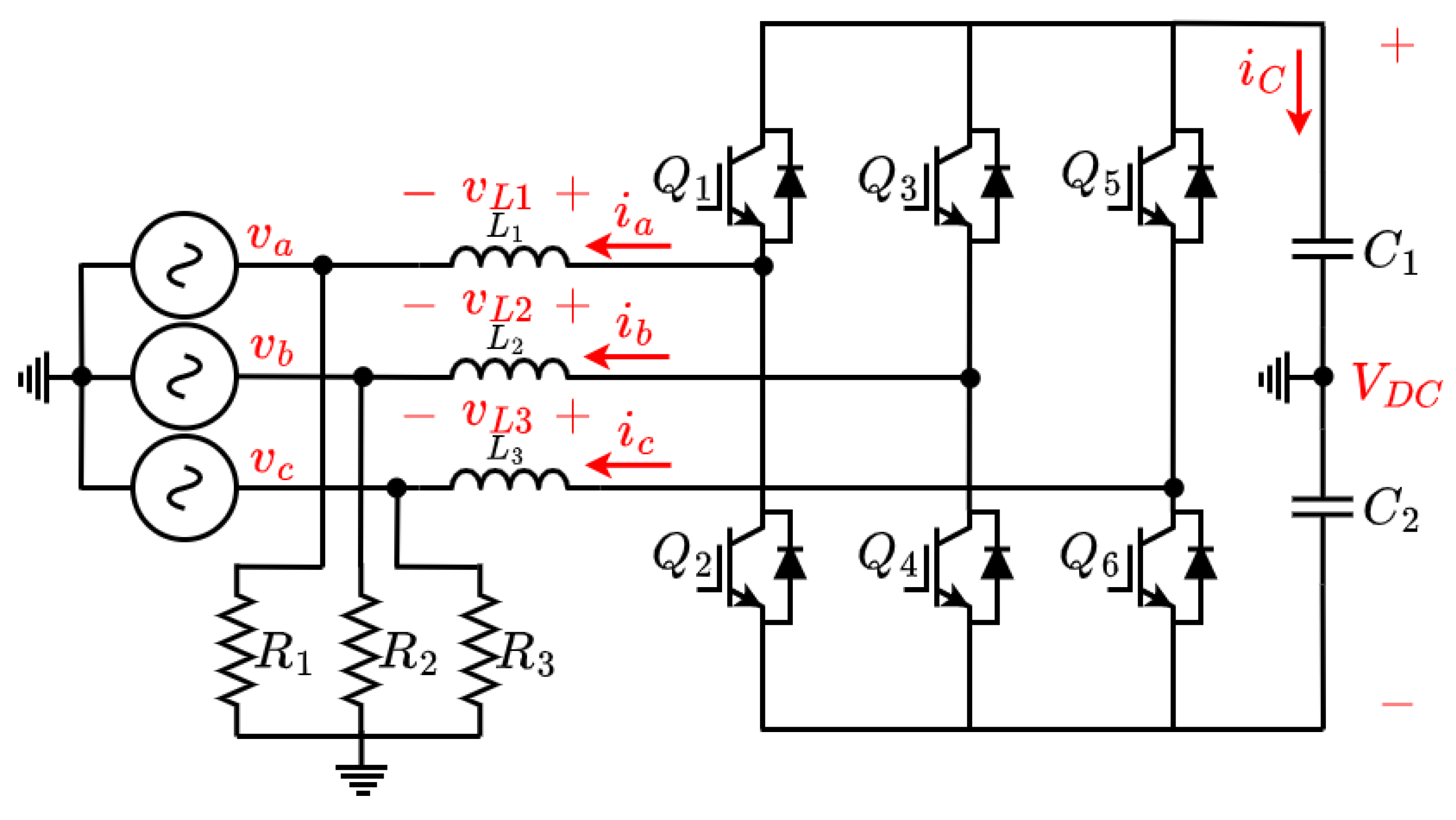
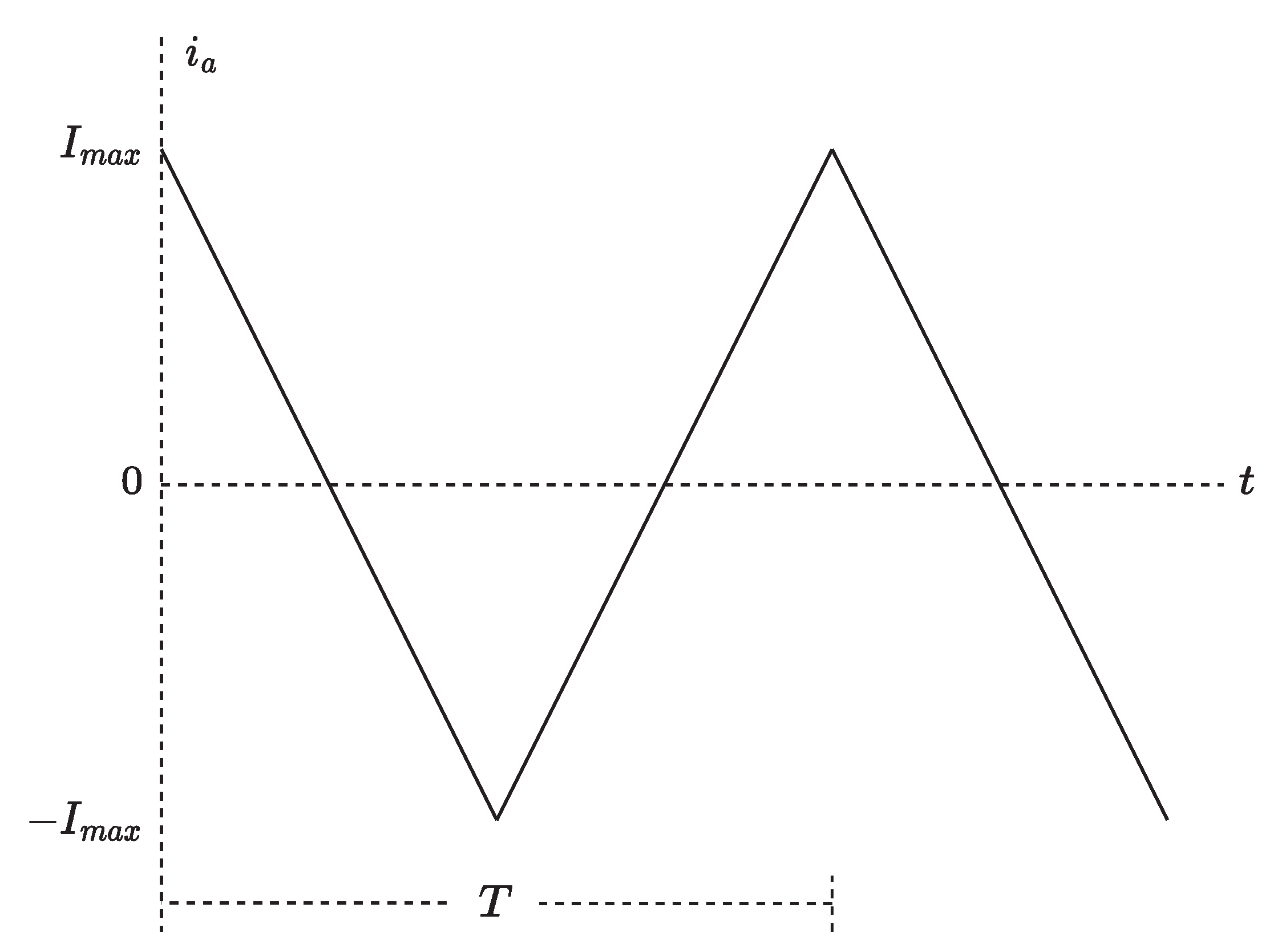
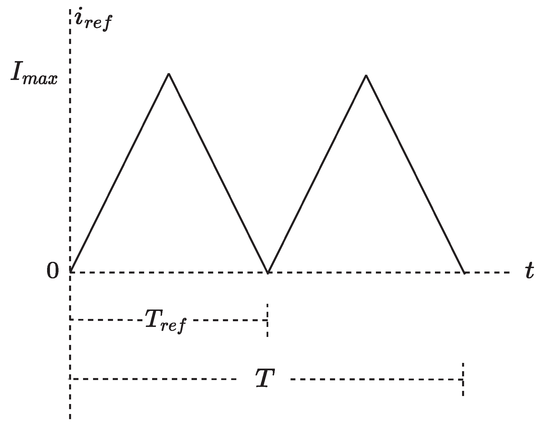
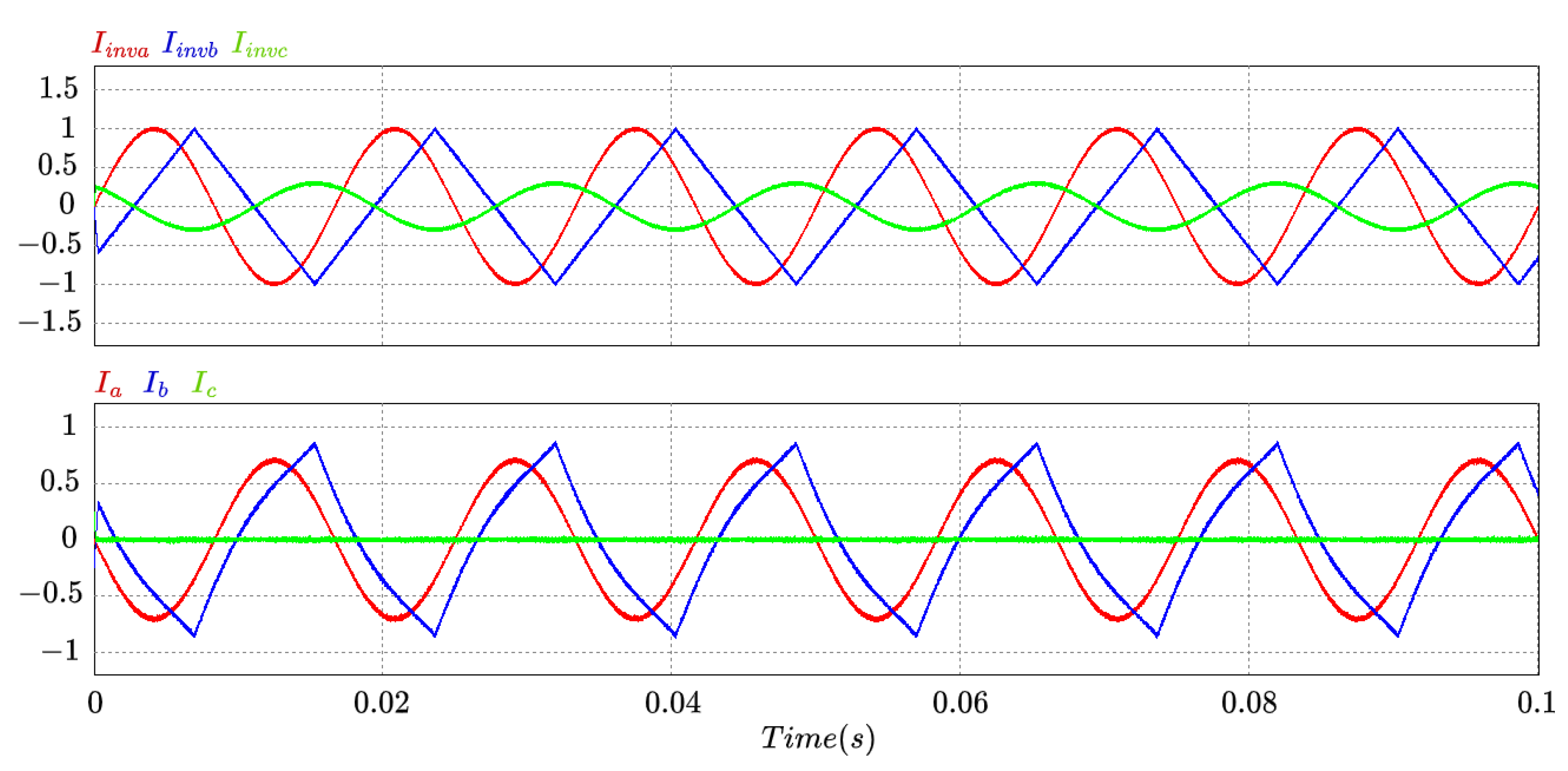
5. UPEL Operation as Distorted Current Source

This section presents an extension of the proposed control for distorted current sources. A triangle shape is used for deduction of equations. In this case, the source is an AC signal single-phase or three-phase. The operation consists of generating a triangle current independent of the AC source waveform. The operation of UPEL as a single-phase rectifier is taken for the validations presented in this section, following the same procedure presented in [24]; nevertheless, this procedure also applies to single-phase and three-phase inverters.

5.1. Mathematical Modeling

The procedure begins with the same differential equations as presented in Equations (2) and (3). Furthermore, Figure 5 shows the triangle waveform (the desired current), while i a is presented in Equation (15), where T is the period.
i a = I m a x 4 I m a x T t     w h e n     0 t T 2 4 I m a x T t 3 I m a x     w h e n     T 2 t T
The current signal is a triangle wave with positive and negative components, similar to a sine wave. Therefore, it is necessary to ensure that the control system receives a rectified reference. Figure 6 shows the waveform of the rectified reference current while its mathematical expression is given by Equation (16). In this case, the reference period ( T r e f ) corresponds to half of the desired current period ( T r e f = T / 2 ). The reference current i r e f is a piecewise signal, with an independent equation for the ascending slope when t is between 0 and T / 2 , and another equation for the descending slope when t is between T / 2 and T. The differential equations for i r e f for each segment are presented in Equation (17).
i r e f = 2 I m a x T r e f t     w h e n     0 t T r e f 2 2 I m a x 2 I m a x T r e f t     w h e n     T r e f 2 t T r e f
i r e f d t = 2 I m a x T r e f     w h e n     0 t T r e f 2 2 I m a x T r e f     w h e n     T r e f 2 t T r e f

5.2. Adaptive Hysteresis Band

Equation (18) corresponds to the AHB for the triangle current. This equation was obtained following the procedure presented in [23] using Equation (16), considering a voltage for the control with the same triangle waveform (15) and T r e f = T / 2 .
A H B = 2 V m a x t L f s w V D C ( V D C 4 V m a x T ) t w h e n     0 t T 4 V m a x L f s w V D C ( 1 2 t T ) [ V D C 2 V m a x ( 1 2 t T ) ]     w h e n     T 4 t T 2

5.3. SMC Validation

This subsection presents the sliding conditions and the control logic for UPEL operation as an AC/DC single-phase rectifier for the sliding surface of Equation (1), following a triangle reference for the input current (as shown in Equation (16)); the procedure is the same as presented in [24]. In this case, i r e f is a signal by parts, and due to this, the sliding condition validations are performed for each part independently.
The stability conditions based on the Lyapunov theorem are fulfilled according to the following equations:
  • Transversality Condition: This evaluates if the converter can be controlled using the control signal u according to Equation (9). This condition is fulfilled considering Equation (19) obtained to solve Equation (9) with Equations (1)–(3), and evaluating in the system limits according to v s . The operation as a single phase (Equation (10)) is more restrictive; therefore, this paper works with this restriction.
    α 1 α 2 < C V r e f L I m a x       w h e n       0 t T 4 C V r e f L I m a x       w h e n       T 4 t T 2
  • Existence Condition: This ensures the existence of sliding mode around S = 0 . The inverter must remain within the sliding surface when S 0 (Equation (11)), ensuring S = 0 with x 1 = x 2 = 0 . Under these conditions, the inverter remains controlled around the equilibrium point.
    Equation (20) provides the second condition for α 1 / α 2 , which was obtained by solving Equation (11) with Equations (1)–(3), evaluating in the boundary of the system in steady state: left side for u = 0 and the right side for u = 1 .
    C R ( 2 I m a x T r e f V s L ) < α 1 α 2 < 2 I m a x T r e f       w h e n       0 t T 4 C R ( 2 I m a x T r e f V s L ) < α 1 α 2 < 2 I m a x V r e f T r e f V s       w h e n       T 4 t T 2
    Finally, the logic control to satisfy the existence condition is presented in Equation (21). This logic is the same for the operation as a DC/DC converter or AC/DC rectifier.
    u ( S ) = 1 2 ( 1 + s i g n ( S ) ) = 1       w h e n       S > 0       a n d       S ˙ < 0 0       w h e n       S < 0       a n d       S ˙ > 0
  • Equivalent control condition: This evaluates the system dynamics under ideal operation conditions ( x 1 = x 2 = 0 ) with infinite switching frequency (Equation (14)) based on Equations (1)–(3). The condition for ensuring the equivalent control ( 0 < u e q < 1 ) corresponds to Equation (22).
    2 I m a x C V r e f T r e f < α 1 α 2 < 2 I m a x C V r e f T r e f                                                             w h e n     0 t T 4 C V r e f ( 2 I m a x T r e f V s L ) < α 1 α 2 < C V r e f ( 2 I m a x T r e f + V s L )     w h e n     T 4 t T 2

6. Simulation Results

This section presents the most relevant results of the UPEL operation. The main objective is to showcase the proposed control with three-phase systems, while [24] details the operation with a single-phase rectifier. Simulations were performed using the PSIM simulator, with some parameters altered to evaluate the UPEL and its control at various operating points. The capacitors have a value of 2200 μF and the inductors 2.2 mH. The sliding coefficients, which are the same for all operating modes, are α 1 = 20 , α 2 = 1 , and α 3 = 1 , considering the constraints of Equations (10) and (12).

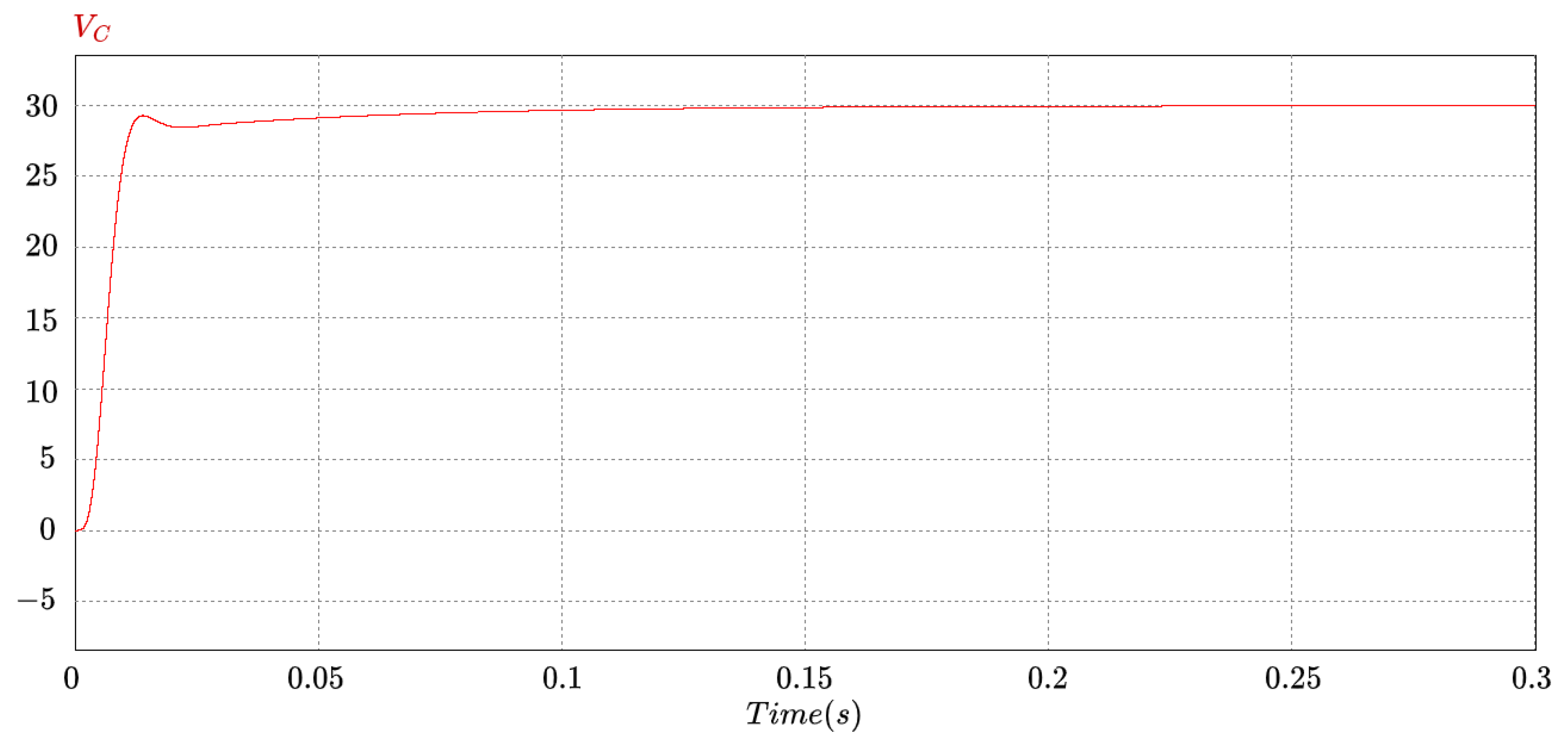
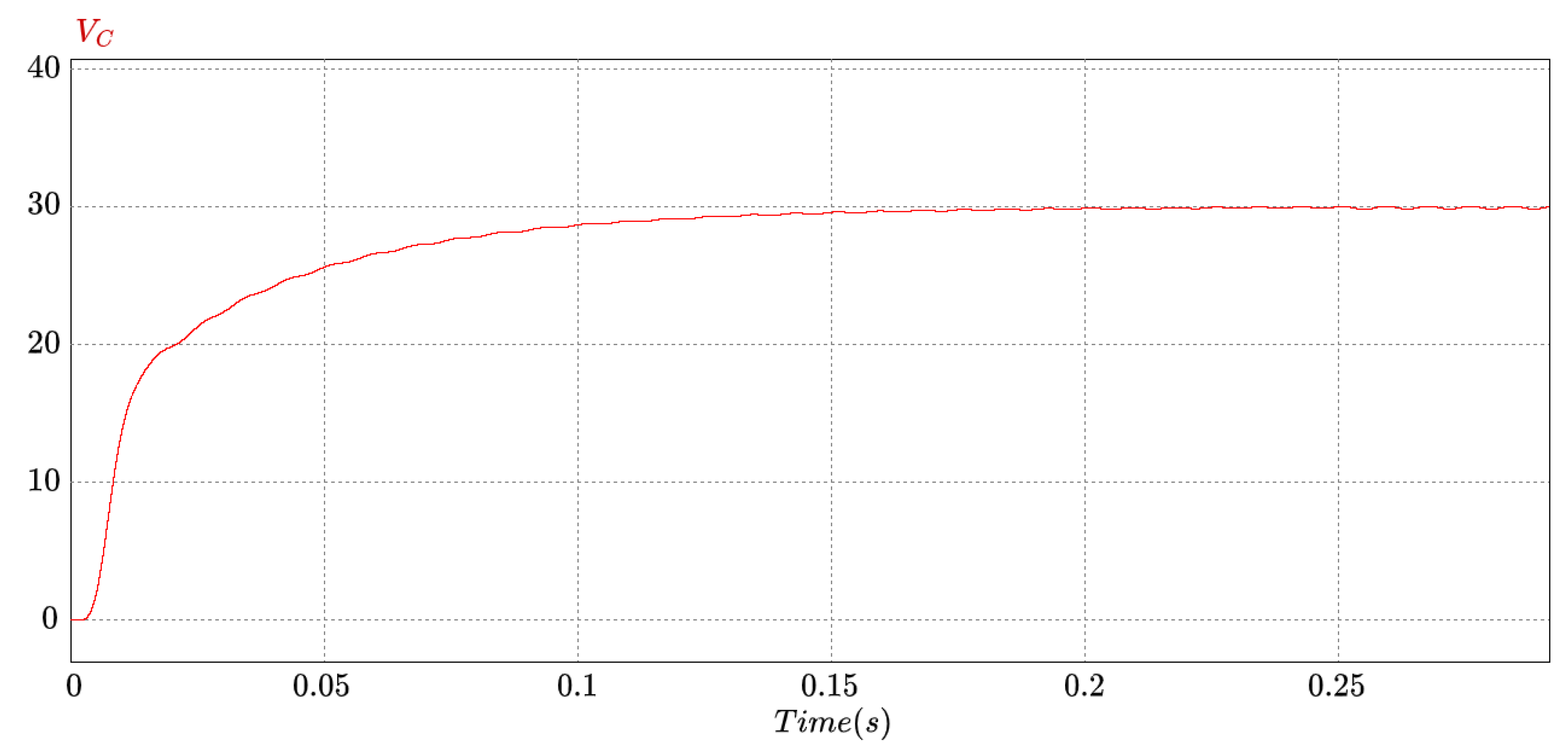
6.1. UPEL Operation as Rectifier

The UPEL circuit in this operation mode is presented in Figure 7, where the load is composed of two resistances of 100   Ω , and the feeding source is 120 V r m s per phase.
The control system is shown in Figure 8. The control corresponds to phase A of the three-phase system; the other phases are a copy of this control considering a gap of 120° between each phase. This control has four stages according to [24]: (1) In the first stage, references are calculated according to Equation (8). (2) In the second stage, the sliding surface is calculated according to Equation (1). (3) In the third stage, AHB is calculated according to Equation (4). (4) finally, the last stage (control) is compared with the sliding surface with AHB, obtaining the control signals to keep the sliding surface into the AHB.
The simulation results are presented in Figure 9 (output voltage) and Figure 10 (input currents). The output voltage stabilizes in approximately 0.14 s for a reference of 30 Vdc. The input currents (phase A in red, phase B in blue, and phase C in green) are sinusoidal in steady state, each with a Total Harmonic Distortion (THD) of approximately 3.2%.
Finally, an additional test was carried out: the reference signal from phase A was changed from sine wave to triangle wave, injecting harmonics into the current to the electrical grid. Figure 11 shows the DC bus voltage for this case. Note that it reaches the reference set point at around 0.2 s, being slower than the sine test. Figure 12 presents the simulation (upper are input currents and low are input voltages), where three results can be highlighted: (1) Signals of currents and voltages are in phase (red phase A, blue phase B, and green phase C). (2) The reference triangle for the current in phase A is satisfactorily followed. (3) The change in the current waveform in phase A does not affect the currents of phases B or C, so that each phase operates independently. It is highlighted that all current signals are in phase with their respective voltage, ensuring a high power factor.
The proposed control meets the objectives for the UPEL operation as three-phase rectifier, additionally, the operation as single-phase rectifier also is fulfilled considering that each branch of the system operates independently.

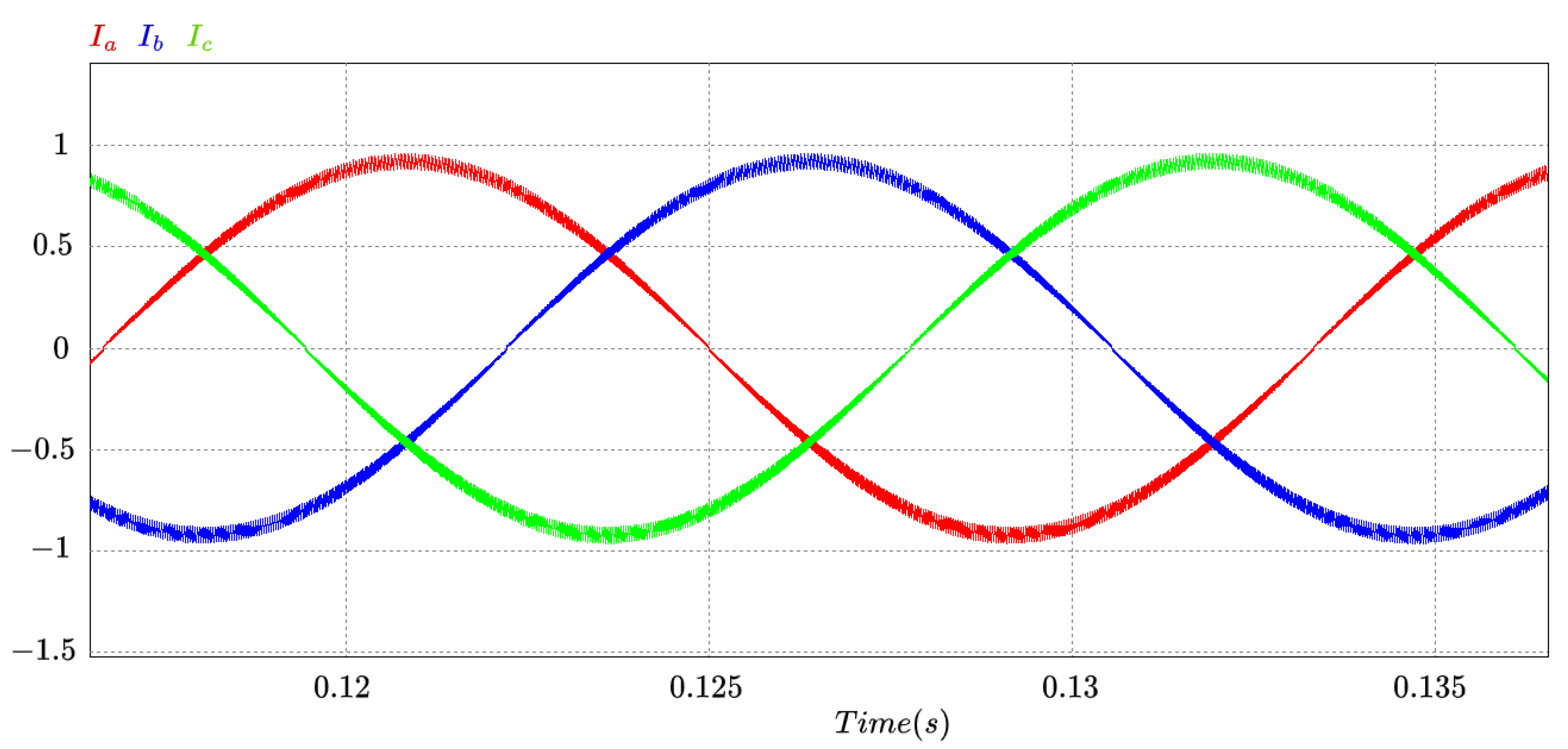
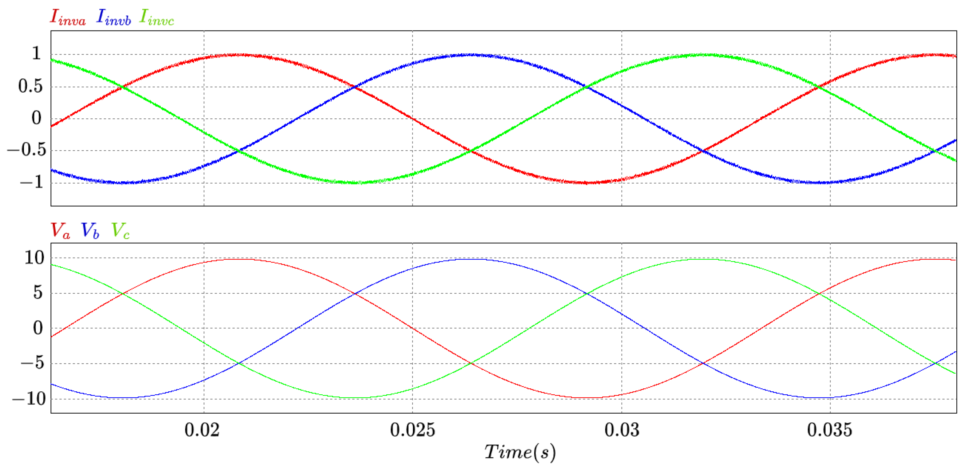
6.2. UPEL Operation as Three-Phase Inverter

The schematic for evaluating the UPEL operation as an inverter is shown in Figure 13. In this case, the inductors were changed by 10 mH, the load is three resistances of 13   Ω , the electrical grid has 20 Vpeak per phase, and the DC bus are two sources of 40 Vdc. The objective of this test consists of validating the sliding surface operating only for current controlling with grid connection.
The control for this operation mode only has two changes: (1) The AHB is modified according to Equation (7) for a three-phase inverter (red square in Figure 14). (2) In this case, the reference current is not calculated by taking load measurements from the load, the current is imposed by the designer.
The load fed by 20 Vpeak without inverter consumes 1.54 Apeak per phase. Then, the first test consists of giving load 1 Apeak. The simulation results are presented in Figure 15, where all currents (upper) are in phase with their respective voltages (low).
The second test is shown in Figure 16. The current amplitude of phase C was increased to 2 Apeak (green color of the figure); consequently, the current from the electrical grid (green color of the lower figure) decreased to 5.38 Apeak.
The simulation results of the last test in this operation mode are presented in Figure 17. Two control actions were performed: (1) The current of inverter phase C (green in the upper figure) has a reference of 15.38 Apeak, so that the inverter supplies all current of load phase C, and then, the grid current for phase C (green in the lower figure) is zero. (2) The angle of current of phase B was changed from 120° to 30 , giving a gap between the grid current and the inverter current of phase B of 90 . It is observed that the control follows the references successfully.

7. Experimental Results

This section presents the most relevant results on the implementation of UPEL. The equipment used in the experimental test is presented in Figure 18, and their main parameters are in Table 2.
The PCB for controlling was built with a TMS320F28335PGFA microcontroller (Texas Instruments, Dallas, TX, USA).
This device operates with Digital Signal Processing to 32-bit with single core, and was programmed with libraries for power electronics applications. In this PCB, the control described in this paper was programmed. The PCB has channels for taking voltage and current measurements, a port for serial communication, and a coupling with power solid-state switches. The current measurement was implemented on a PCB with sensors ACS714 (Allegro MicroSystems, Manchester, NH, USA) and the PCB for voltage measurement has sensors AMC1200 (Texas Instruments, Dallas, TX, USA). The power switch PCB has an IRAM136-3063 (Infineon Technologies. Neubiberg, Germany) with internal gate drivers. Measurements were taken with a digital oscilloscope ROHDE & SCHWARZ 388 RTH1004 (Rohde & Schwarz. Munich, Germany). The DC bus consists of an adjustable array of four capacitors of 2200 μF each; similarly, the inductors are modular and adjustable.

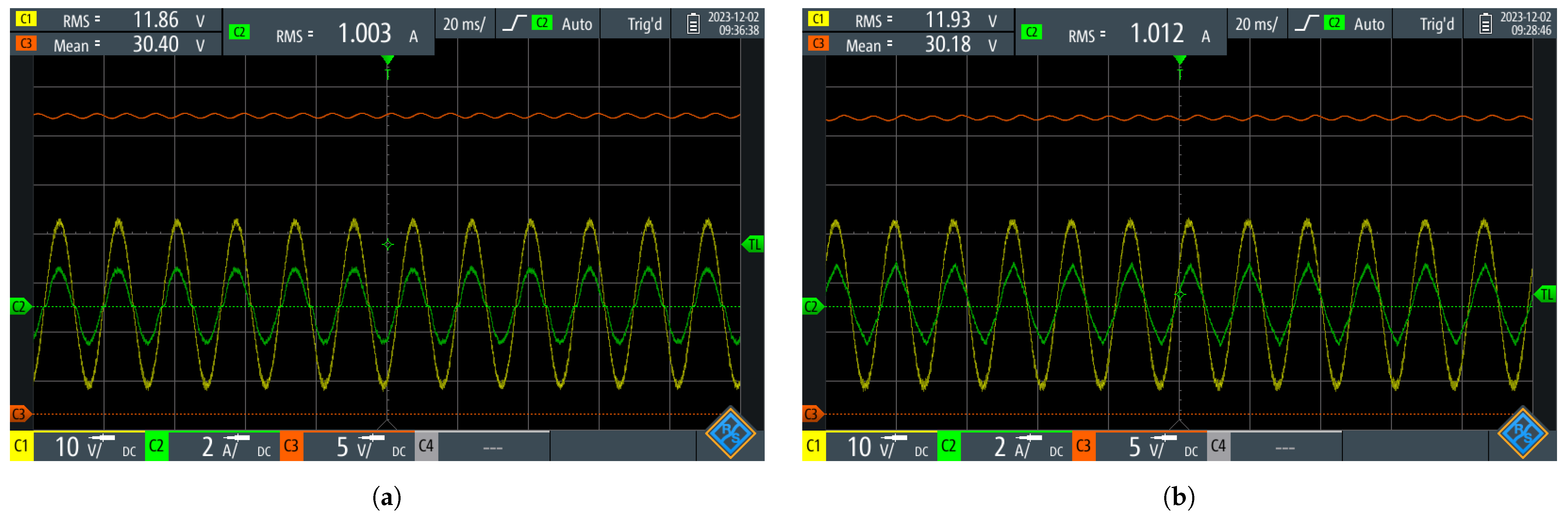
7.1. First Test: Controlled Rectifier

Figure 19 presents the UPEL operation as a single-phase rectifier with power factor correction and DC bus voltage control; input voltage is 12 Vrms (yellow) and output voltage reference is 30 Vdc (Figure 9). Figure 19a shows the input current (green) with a sine reference signal; the input current value is 1 Arms. Figure 19b shows the input current (green) with a triangle reference signal; the input current value is the same, 1 Arms. In both cases, a DC bus voltage (red) can be obtained according to the reference independent of the input current waveform. The single-phase experimental results confirm the effectiveness of the ASPWM strategy in maintaining voltage stability and ensuring power factor correction. The obtained waveforms validate the ability of the UPEL to follow sinusoidal and triangular current references while keeping the DC bus voltage at the desired setpoint. The transition between reference waveforms, as shown in Figure 19a,b, demonstrates the robustness of the control strategy under steady-state conditions.
Additionally, Figure 20 presents the UPEL behavior in the face of load changes, in this case, the load was doubled following the triangle reference; to achieve this, the load resistance was suddenly changed connecting a resistance in parallel with the same value in order to validate the control response in face of disturbances. Two main responses are observed: (1) The output voltage mean value follows the reference (without undershoot or overshot) even though the oscillations have increased due to the load. (2) The input current reaches 2 Arms, with a small transient of 0.434 ms, and UPEL continues its normal operation. The system response to load variations, depicted in Figure 20, highlights the stability of the ASPWM approach. The DC bus voltage remains regulated with minimal transient effects, indicating that the sliding-mode control effectively compensates for abrupt changes in load demand. The quick adaptation of the current reference to maintain power factor correction confirms the applicability of this methodology in dynamic load scenarios.
Figure 21 presents the behavior of UPEL in the three-phase mode. In this test, phase a (yellow) has a current reference of 2.2 Apeak, phase B (green) has a current reference of 0 Apeak and phase C (red) has a current reference of 2.2 Apeak. Phases A and C are observed to operate normally, and the DC bus is approximately 30 Vdc (following the reference). The three-phase experimental results further validate the proposed ASPWM control strategy, demonstrating its ability to independently regulate each phase while ensuring proper energy quality. Figure 21 shows the UPEL capability to control phase currents, even when one of the phases (Phase B) is set to zero. The DC bus voltage remains stable at approximately 30 Vdc, which confirms that the system can manage unbalanced loads without compromising the operation of the other phases.
Finally, Table 3 shows a summary of the most important parameters and results analyzed in this subsection.

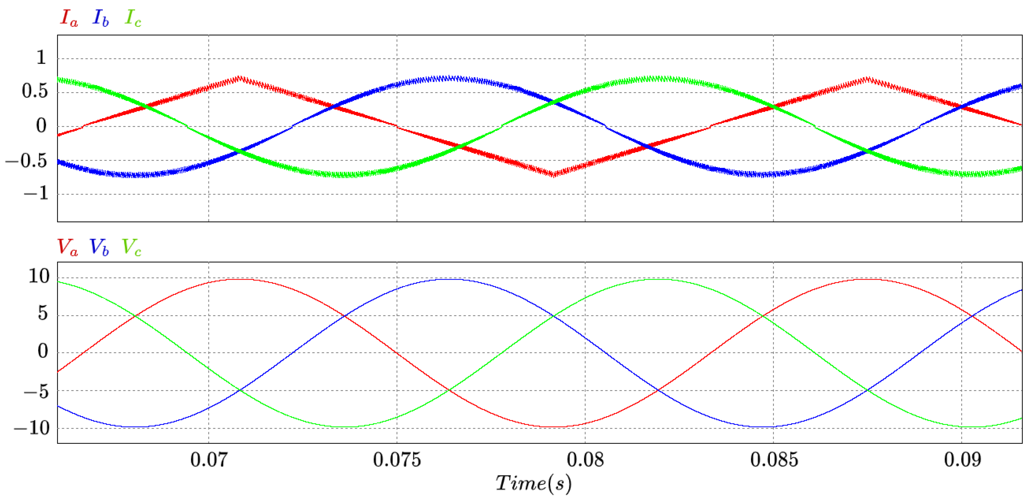
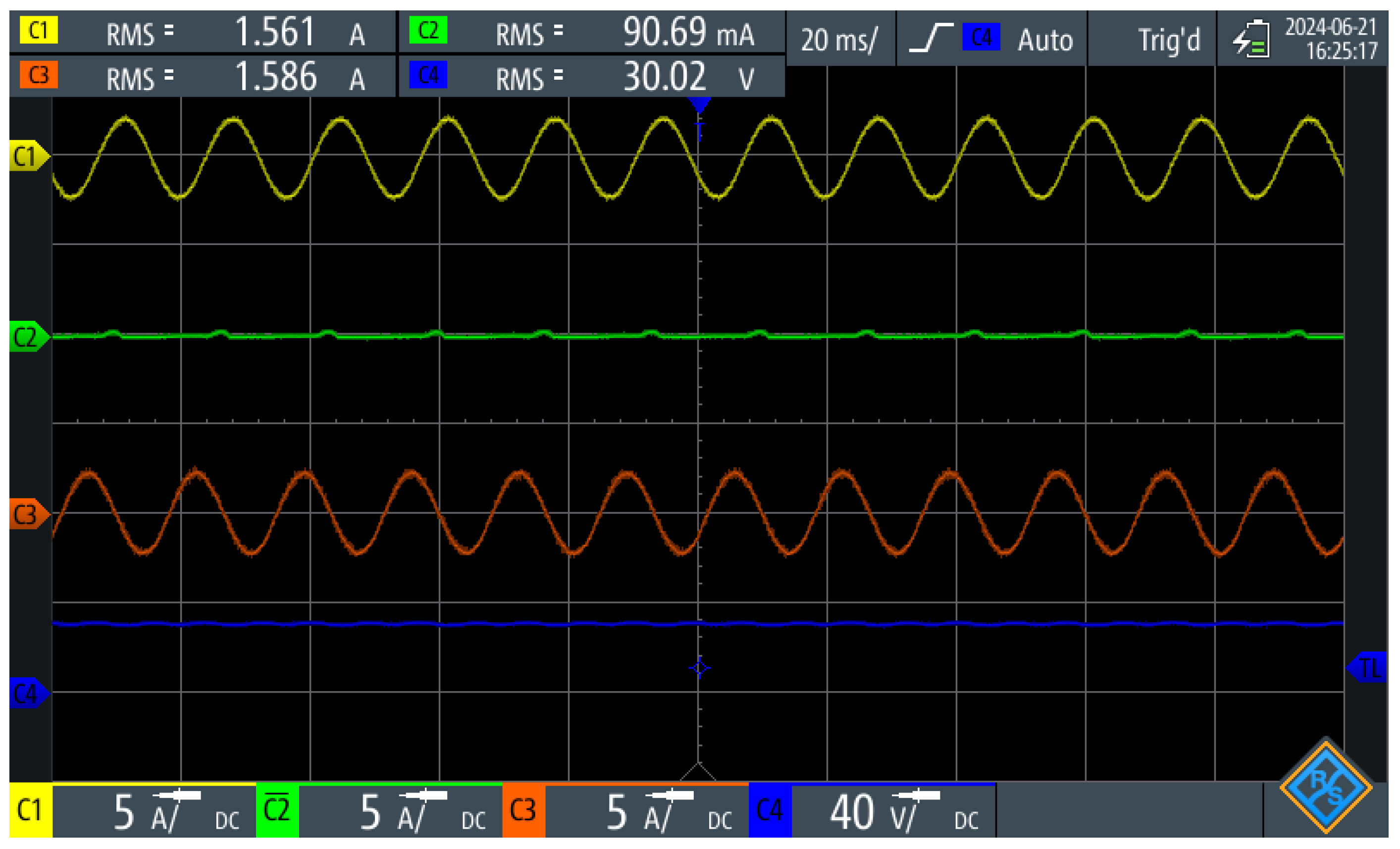
7.2. Second Test: Inverter

Figure 22 shows the results of the UPEL operating as a three-phase inverter with the phase A grid voltage (blue), the phase A current (yellow), the phase B current (green), and the phase C current (red). Figure 22a presents the UPEL operating as a balanced system; current and voltage of phase A are in phase, and other currents have a gap of 120 , indicating proper synchronization and control of the three-phase inverter with power factor correction. Figure 22b shows the results of injecting unbalances and harmonics into the grid. In this case, the current of phase A has a gap of 90 (inductive power factor p f = 0 ) following a triangle reference signal (mainly with harmonics 3, 5, and 7). Phases B and C have a gap of 180 and 270 , respectively; it is highlighted that this change in phase A does not affect the waveform of the other sinusoidal signals. These results confirm that the UPEL can independently modify the current waveform of a single phase without affecting the others, demonstrating the robustness of the proposed control strategy in energy quality applications.
Finally, Figure 23 presents the UPEL behavior in the face of load changes. In this case, phase B begins at zero, then, a load that consumes two times the currents of other phases is connected. The UPEL references are successfully followed, ensuring that changes, disturbances, and control actions in each phase do not affect the behavior of the other phases. The results indicate that the UPEL successfully adjusts its reference values, ensuring that each phase operates independently without affecting the stability of the other phases. The control strategy dynamically adapts to the new load condition while maintaining system stability, confirming the effectiveness of the ASPWM method in managing unbalanced loads and grid disturbances in this operation mode.
Finally, Table 4 shows a summary of the most important parameters and results analyzed in this subsection.

8. Conclusions

In this paper, the development of a three-phase universal programming electronic load (UPEL) and its validation through simulation and experimental results of the advanced control technique, Adaptive Sliding Pulse Width Modulation (ASPWM), were presented. The proposed ASPWM integrates sliding-mode control with frequency limitation and an Adaptive Hysteresis Band. The results demonstrate that the proposed sliding surface can be effectively utilized for all operational modes, including single-phase and three-phase, controlled rectifier and inverter, with functions such as power factor variation and Total Harmonic Distortion (THD) modification, and the capability of injecting harmonics into the grid. The proposed ASPWM significantly improves energy quality by enabling precise control of active and reactive power, harmonic injection, and operation across multiple modes, including AC/DC rectification and DC/AC inversion. Both simulation and experimental results validate the effectiveness of ASPWM in improving performance metrics and ensuring operational stability. The UPEL showed currents in phase with their respective voltages and successfully followed the reference signals, demonstrating a high power factor and robust control under load changes. Additionally, the results indicate that the UPEL can effectively shape the injected current waveform according to a predefined reference, including sinusoidal and nonsinusoidal waveforms. The precise tracking of the triangular waveform reference in a phase, while maintaining sinusoidal behavior in the other phases, highlights the versatility of the ASPWM approach in active power filtering applications.

Author Contributions

Conceptualization, J.R.O.-C., N.M.-G., S.D.S.-Z., and J.M.L.-L.; data curation, J.R.O.-C.; formal analysis, J.R.O.-C., N.M.-G., S.D.S.-Z., and J.M.L.-L.; funding acquisition, J.M.L.-L. and N.M.-G.; investigation, J.R.O.-C., N.M.-G., S.D.S.-Z., and J.M.L.-L.; methodology, J.R.O.-C., N.M.-G., S.D.S.-Z., and J.M.L.-L.; project administration, S.D.S.-Z. and N.M.-G.; resources, S.D.S.-Z., N.M.-G., and J.M.L.-L.; software, J.R.O.-C.; supervision, N.M.-G. and J.M.L.-L.; validation, J.R.O.-C.; test, J.R.O.-C. and S.B.-C.; visualization, J.R.O.-C., N.M.-G., S.D.S.-Z., and J.M.L.-L.; writing—original draft, J.R.O.-C.; writing—review and editing, J.R.O.-C., N.M.-G., S.D.S.-Z., and J.M.L.-L. All authors have read and agreed to the published version of the manuscript.

Funding

This research was funded by the Colombia Scientific Program within the framework of the so-called Ecosistema Científico (Contract No. FP44842-218-2018). The main author also thanks the “Institución Universitaria Pascual Bravo” for its financial support under the “Talento Pascualino” program.

Data Availability Statement

The original contributions presented in this study are included in the article. Further inquiries can be directed to the corresponding author.

Acknowledgments

The authors appreciate the support from the “Institución Universitaria Pascual Bravo” through the project “Talento Pascualino”. The authors also gratefully acknowledge the financial support provided by the Bicentenary Doctoral Excellence Scholarship Program, Court 1, with agreement number 20230017-20-20, under the call of the Science, Technology and Innovation Fund of the General System of Royalties (High Level Training Project Universidad de Antioquia National BPIN 2019000100017).

Conflicts of Interest

The authors declare that they have no conflicts of interest.

References

  1. Medina-Ortega, C.E.; Patiño-Noguera, M.A.; Revelo-Fuelagán, J.; Candelo-Becerra, J.E. Programmable Electronic Load Prototype for the Power Quality Analysis of an Experimental Microgrid. Sustainability 2022, 14, 11258. [Google Scholar] [CrossRef]
  2. Davis, P.N.; Wright, P.S. An Electronic Load to Verify Harmonic Emission Compliance. IEEE Trans. Instrum. Meas. 2017, 66, 1446–1453. [Google Scholar] [CrossRef]
  3. Geng, Z.; Gu, D.; Hong, T.; Czarkowski, D. Programmable Electronic AC Load Based on a Hybrid Multilevel Voltage Source Inverter. IEEE Trans. Ind. Appl. 2018, 54, 5512–5522. [Google Scholar] [CrossRef]
  4. De Rezende, G.M.; De Almeida, M.V.; Sá Ferreira, T.D.; De Sousa, C.V.; Mendes, V.F. Regenerative Active Electronic Load With Current, Voltage and Frequency Control for Power Transformer Testing. IEEE Access 2021, 9, 65319–65329. [Google Scholar] [CrossRef]
  5. Yang, Q.; He, M.; Xu, J.h.; Li, X.; Zhu, J.; Zhang, Z.; Gu, Z.; Ren, X.; Chen, Q. Wide Input Voltage DC Electronic Load Architecture With SiC MOSFETs for High Efficiency Energy Recycling. IEEE Trans. Power Electron. 2020, 35, 13053–13067. [Google Scholar] [CrossRef]
  6. Park, B.W.; Park, S.J.; Kang, F.S. Electronic Load System With Interleaved Structure Applicable to DC, Single-Phase AC, and Three-Phase AC. IEEE Access 2022, 10, 58677–58688. [Google Scholar] [CrossRef]
  7. Upadhyay, S.; Mishra, S.; Joshi, A. A Wide Bandwidth Electronic Load. IEEE Trans. Ind. Electron. 2012, 59, 733–739. [Google Scholar] [CrossRef]
  8. Primavera, S.; Rella, G.; Maddaleno, F.; Smedley, K.; Abramovitz, A. One-cycle controlled three-phase electronic load. IET Power Electron. 2012, 5, 827–832. [Google Scholar] [CrossRef]
  9. Kazerani, M. A high-performance controllable AC load. In Proceedings of the 2008 34th Annual Conference of IEEE Industrial Electronics, Orlando, FL, USA, 10–13 November 2008; pp. 442–447. [Google Scholar] [CrossRef]
  10. Younsi, S.; Hamrouni, N. Control of Grid Connected Three-Phase Inverter for Hybrid Renewable Systems using Sliding Mode Controller. Int. J. Adv. Comput. Sci. Appl. 2018, 9, 336–341. [Google Scholar] [CrossRef]
  11. Mahlooji, M.H.; Mohammadi, H.R.; Rahimi, M. A review on modeling and control of grid-connected photovoltaic inverters with LCL filter. Renew. Sustain. Energy Rev. 2018, 81, 563–578. [Google Scholar] [CrossRef]
  12. Roodsari, B.N.; Nowicki, E.P. Analysis and Experimental Investigation of the Improved Distributed Electronic Load Controller. IEEE Trans. Energy Convers. 2018, 33, 905–914. [Google Scholar] [CrossRef]
  13. Zhang, Z.; Liu, X.; Zhang, Y.; Zhang, C.; Deng, W. A Novel Current Control Method Based on Dual-Mode Structure Repetitive Control for Three-Phase Power Electronic Load. IEEE Access 2021, 9, 144406–144416. [Google Scholar] [CrossRef]
  14. Errouissi, R.; Muyeen, S.M.; Al-Durra, A.; Leng, S. Experimental Validation of a Robust Continuous Nonlinear Model Predictive Control Based Grid-Interlinked Photovoltaic Inverter. IEEE Trans. Ind. Electron. 2016, 63, 4495–4505. [Google Scholar] [CrossRef]
  15. de Brito, M.A.G.; Dourado, E.H.B.; Sampaio, L.P.; da Silva, S.A.O.; Garcia, R.C. Sliding Mode Control for Single-Phase Grid-Connected Voltage Source Inverter with L and LCL Filters. Eng 2023, 4, 301–316. [Google Scholar] [CrossRef]
  16. Rayane, K.; Bougrine, M.; Benalia, A.; Guesmi, K. Sliding Mode Control of a Three-Phase Inverter with an Output LC Filter. In Proceedings of the 2018 International Conference on Applied Smart Systems (ICASS), Medea, Algeria, 24–25 November 2018; pp. 1–4. [Google Scholar] [CrossRef]
  17. Guo, B.; Su, M.; Wang, H.; Tang, Z.; Liao, Y.; Zhang, L.; Shi, S. Observer-based second-order sliding mode control for grid-connected VSI with LCL-type filter under weak grid. Electr. Power Syst. Res. 2020, 183, 106270. [Google Scholar] [CrossRef]
  18. Dang, C.; Tong, X.; Song, W. Sliding-mode control in dq-frame for a three-phase grid-connected inverter with LCL-filter. J. Frankl. Inst. 2020, 357, 10159–10174. [Google Scholar] [CrossRef]
  19. Sufyan, A.; Jamil, M.; Ghafoor, S.; Awais, Q.; Ahmad, H.A.; Khan, A.A.; Abouobaida, H. A Robust Nonlinear Sliding Mode Controller for a Three-Phase Grid-Connected Inverter with an LCL Filter. Energies 2022, 15, 9428. [Google Scholar] [CrossRef]
  20. Liang, Y.; Nwankpa, C. A power-line conditioner based on flying-capacitor multilevel voltage-source converter with phase-shift SPWM. IEEE Trans. Ind. Appl. 2000, 36, 965–971. [Google Scholar] [CrossRef]
  21. Yu, H.; Chen, B.; Yao, W.; Lu, Z. Hybrid Seven-Level Converter Based on T-Type Converter and H-Bridge Cascaded Under SPWM and SVM. IEEE Trans. Power Electron. 2018, 33, 689–702. [Google Scholar] [CrossRef]
  22. Chincholkar, S.H.; Jiang, W.; Chan, C.Y. A Modified Hysteresis-Modulation-Based Sliding Mode Control for Improved Performance in Hybrid DC–DC Boost Converter. IEEE Trans. Circuits Syst. II Express Briefs 2018, 65, 1683–1687. [Google Scholar] [CrossRef]
  23. Mejía-Ruiz, G.E.; Muñoz-Galeano, N.; Ortiz-Castrillón, J.R. Banda de Histéresis Adaptativa para un Convertidor AC-DC Elevador sin Puente, con Correccion del Factor de Potencia y Control por Modos Deslizantes. Inf. Tecnológica 2019, 30, 283–292. [Google Scholar] [CrossRef]
  24. Ortiz-Castrillón, J.R.; Mejía-Ruiz, G.E.; Muñoz-Galeano, N.; López-Lezama, J.M.; Cano-Quintero, J.B. A Sliding Surface for Controlling a Semi-Bridgeless Boost Converter with Power Factor Correction and Adaptive Hysteresis Band. Appl. Sci. 2021, 11, 1873. [Google Scholar] [CrossRef]
  25. Ortiz-Castrillón, J.R.; Saldarriaga-Zuluaga, S.D.; Muñoz-Galeano, N.; López-Lezama, J.M.; Benavides-Córdoba, S.; Cano-Quintero, J.B. Optimal Sliding-Mode Control of Semi-Bridgeless Boost Converters Considering Power Factor Corrections. Energies 2023, 16, 6282. [Google Scholar] [CrossRef]
  26. International Electrotechnical Commission. IEC 61000-3-2; Electromagnetic compatibility (EMC)—Part 3-2: Limits—Limits for harmonic current emissions (equipment input current lower or equal 16 A per phase). International Electrotechnical Commission: Geneva, Switzerland, 2020. [Google Scholar]
  27. Institute of Electrical and Electronics Engineers. IEEE 519-2022; IEEE Recommended Practice and Requirements for Harmonic Control in Electric Power Systems. Institute of Electrical and Electronics Engineers: New York, NY, USA, 2022. [Google Scholar]
Figure 1. Three-phase inverter topology to implement: three branches, four wires.
Electronics 14 01100 g001
Figure 2. Adaptive Hysteresis Band scheme used to limit the ripple variation.
Electronics 14 01100 g002
Figure 3. Three-phase topology configuration for the UPEL operation as controlled rectifier. (a) AC/DC three-phase Boost converter: positive half-cycle. (b) AC/DC three-phase Boost converter: negative half-cycle.
Electronics 14 01100 g003
Figure 4. Three-phase topology configured to operate as DC/AC inverter.
Electronics 14 01100 g004
Figure 5. Reference triangle wave form for the UPEL current.
Electronics 14 01100 g005
Figure 6. Rectified triangle waveform for the UPEL reference current.
Electronics 14 01100 g006
Figure 7. Schematic for UPEL operation as controlled rectifier; simulation software: PSIM 9.1.
Electronics 14 01100 g007
Figure 8. Control system by the three-phase rectifier: sliding surface according Equation (1), Adaptive Hysteresis Band according to Equation (7), and control according to Figure 2.
Electronics 14 01100 g008
Figure 9. UPEL operation as three-phase rectifier: output DC voltage.
Electronics 14 01100 g009
Figure 10. UPEL operation as three-phase rectifier: input current per phase.
Electronics 14 01100 g010
Figure 11. UPEL operation as three-phase rectifier: output voltage stabilization with triangle current reference in phase A.
Electronics 14 01100 g011
Figure 12. UPEL operation as three-phase rectifier: upper: input currents with triangle reference in phase A; lower: grid voltage in phase with its corresponding current.
Electronics 14 01100 g012
Figure 13. Schematic for the UPEL operation as three-phase inverter in PSIM 9.1.
Electronics 14 01100 g013
Figure 14. Control system for the three-phase inverter. Control from Figure 8 modified according to Equation (7).
Electronics 14 01100 g014
Figure 15. Output currents of the three-phase inverter.
Electronics 14 01100 g015
Figure 16. Three-phase inverter results: change in reference amplitude of phase C and other phases without changes.
Electronics 14 01100 g016
Figure 17. Three-phase inverter results: upper: change in amplitude (reduction) of phase C, following a triangle reference in phase B (change in amplitude and phase); lower: response of the feeding source currents.
Electronics 14 01100 g017
Figure 18. Three-phase inverter built for UPEL implementation.
Electronics 14 01100 g018
Figure 19. Validation of adequate control behavior (power factor correction, following) sine and triangle wave forms for the input current: (a) Input current with sine reference signal. (b) Input current with triangle reference signal.
Electronics 14 01100 g019
Figure 20. Validation of adequate control behavior in face of load changes; in this case, the UPEL in normal operation with triangular current doubles its load at a random time.
Electronics 14 01100 g020
Figure 21. Validation of adequate control behavior in face of load changes; in this case, phase B follows a reference of zero.
Electronics 14 01100 g021
Figure 22. Validation of adequate control behavior with sine (left) and triangle (right) waveforms for the input current: (a) Input current with sine reference signal. (b) Input current with triangle reference signal.
Electronics 14 01100 g022
Figure 23. Validation of adequate control behavior in the face of load changes; in this case, phase B change from 0 up to 2 Arms.
Electronics 14 01100 g023
Table 1. Comparison of ASPWM with SPWM, SVM, and Hysteresis-Based SMC.
FeatureASPWMSPWMSVMHysteresis SMC
Switching Frequency StabilityFixedFixedFixedVariable
Harmonic Distortion (THD)LowModerateLowHigh
Dynamic Response SpeedFastSlowModerateFast
Computational ComplexityModerateLowHighLow
Power Factor ControlYesLimitedYesLimited
Performance with Nonlinear LoadsExcellentPoorGoodModerate
Frequency StabilityHighHighHighLow
Harmonic Injection CapabilityYesNoLimitedLimited
Robustness to Parameter VariationsHighLowModerateHigh
Implementation ComplexityModerateLowHighLow
Table 2. Features of the UPEL.
ParameterValue
Grid voltage ( v s ) 12 Vrms, 60 Hz
DC bus capacitor ( C ) 2200 μF
DC bus voltage ( V o ) 30 V
Inductors ( L 1 = L 2 = L ) 23 mH–10 mH
Switching frequency ( f s w ) 40 kHz
Load ( R ) 108
Table 3. Summary of experimental results for the controlled rectifier tests.
ParameterSingle Phase ResultsThree Phase Results
Input Voltage (RMS)12 V12 V per phase
DC Bus Voltage30 V30 V
Load Resistance108  Ω 3 × 10⁸  Ω
Switching Frequency40 kHz40 kHz
Input Current (RMS)1 A1.56 A (Phase A, C), 0 A (Phase B)
Current Reference WaveformSinusoidal/TriangularSinusoidal/Triangular (Phase A)
Power Factor (PF)≈0.99≈0.99
Transient Response (Load Step)<0.5 ms<1 ms
Table 4. Summary of experimental results for the three-phase inverter.
ParameterMeasured Value
Grid voltage ( V s )12 Vrms, 60 Hz
DC bus voltage ( V o )30 V
Phase A current (balanced)1.54 Apeak
Phase A current (distorted)1 Apeak, Phase shift: 90°, Triangle waveform
Phase B and C currentsBalanced: 120° shift, Unbalanced: 180° and 270° shift
Phase B load variationInitial: 0 A, Final: 2 Apeak
THD in currentAdjustable
Power factorAdjustable
Disclaimer/Publisher’s Note: The statements, opinions and data contained in all publications are solely those of the individual author(s) and contributor(s) and not of MDPI and/or the editor(s). MDPI and/or the editor(s) disclaim responsibility for any injury to people or property resulting from any ideas, methods, instructions or products referred to in the content.

