Article

Investigation of Source/Drain Height Variation and Its Impacts on FinFET and GAA Nanosheet FET

1
School of Microelectronics, Xidian University, Xi’an 710071, China
2
Department of Electrical and Computer Engineering, McMaster University, Hamilton, ON L8S 4K1, Canada
*
Author to whom correspondence should be addressed.
Electronics 2025, 14(6), 1091; https://doi.org/10.3390/electronics14061091
Submission received: 11 February 2025 / Revised: 28 February 2025 / Accepted: 2 March 2025 / Published: 10 March 2025
(This article belongs to the Section Semiconductor Devices)

Abstract

:
As semiconductor technology and process nodes advance, three-dimensional devices like FinFET and NSFET are increasingly becoming the primary choice, replacing planar MOSFETs. However, the complex manufacturing processes and high process sensitivity of three-dimensional devices at advanced process nodes inevitably cause significant deviations from the ideal structure during actual fabrication, leading to notable changes in their electrical characteristics. This paper investigates the impact of source/drain region height fluctuations caused by etching and epitaxial growth variations on the electrical characteristics of FinFET and NSFET devices, as well as their related circuits. The electrical characteristics when height variations occur in single and multiple electrodes indicate that, although NSFET and FinFET generally exhibit similar properties such as a decrease in the ON-state current when the source/drain height is reduced, the independent nature of the nanosheets in NSFET and the unidirectional conduction of Schottky contact resistance cause significant differences in their electrical characteristics. Additionally, the related circuit-level simulations show that height fluctuations in the source/drain regions of devices can significantly impact circuit characteristics, including voltage and delay, and in severe cases, they may even lead to circuit failure.

1. Introduction

As semiconductor process nodes continue to shrink, three-dimensional devices such as FinFET and NSFET are gradually replacing planar MOSFET as the main device structures in advanced nodes [1]. Furthermore, due to better gate control capabilities, NSFETs are considered the most promising candidate device structures for nodes below 3 nm [2,3]. However, the complex manufacturing processes of three-dimensional devices, combined with a higher sensitivity to process variations at advanced nodes, place higher demands on lithography, etching, deposition, and other processes. Due to the aforementioned reasons, devices in actual production often deviate from the ideal situation because of process variations and process deviations, resulting in changes in device characteristics [4,5]. Currently, many papers investigate the impact of process variations and deviations on advanced devices such as NSFETs and FinFETs, including the effects of channel dimensions and geometries [6], process angles [7], non-ideal etching [8], and defects under severe process deviations on the electrical characteristics of the devices [9,10]. In recent years, numerous papers have reported instances of source/drain height variations in manufacturing processes due to deviations in epitaxial growth and etching processes [11,12,13]. Additionally, existing studies have analyzed the impact of the recess process on the source/drain regions and the electrical characteristics of the devices [14]. Considering the high compatibility between NSFET and FinFET processes, the aforementioned process deviations related to the source/drain in FinFET are also likely to occur in NSFET devices [15]. However, due to the multi-layer stacked structure of NSFET devices in the vertical direction, the impact of source/drain height variations caused by deviations in etching and epitaxial processes on their electrical characteristics is significantly different from that of FinFET devices. Currently, there are few analyses on the impact of source/drain height fluctuations on the electrical characteristics of NSFET devices. To deeply investigate the impact of source/drain height variations caused by process fluctuations on the electrical characteristics of devices, this paper simulates different source/drain heights in FinFET and NSFET devices. Additionally, it explores the influence of these variations on circuit-level performance using an INV cell, NAND cell, and five-stage ring oscillator (RO) circuits.

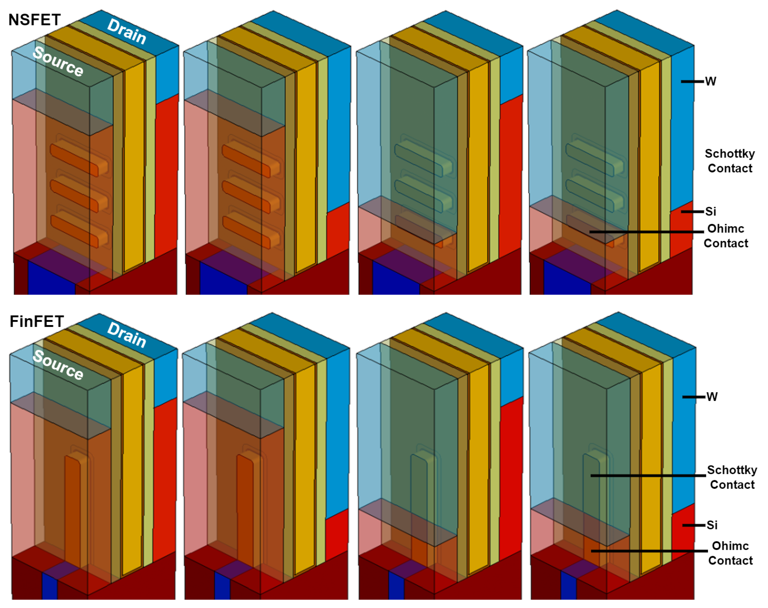
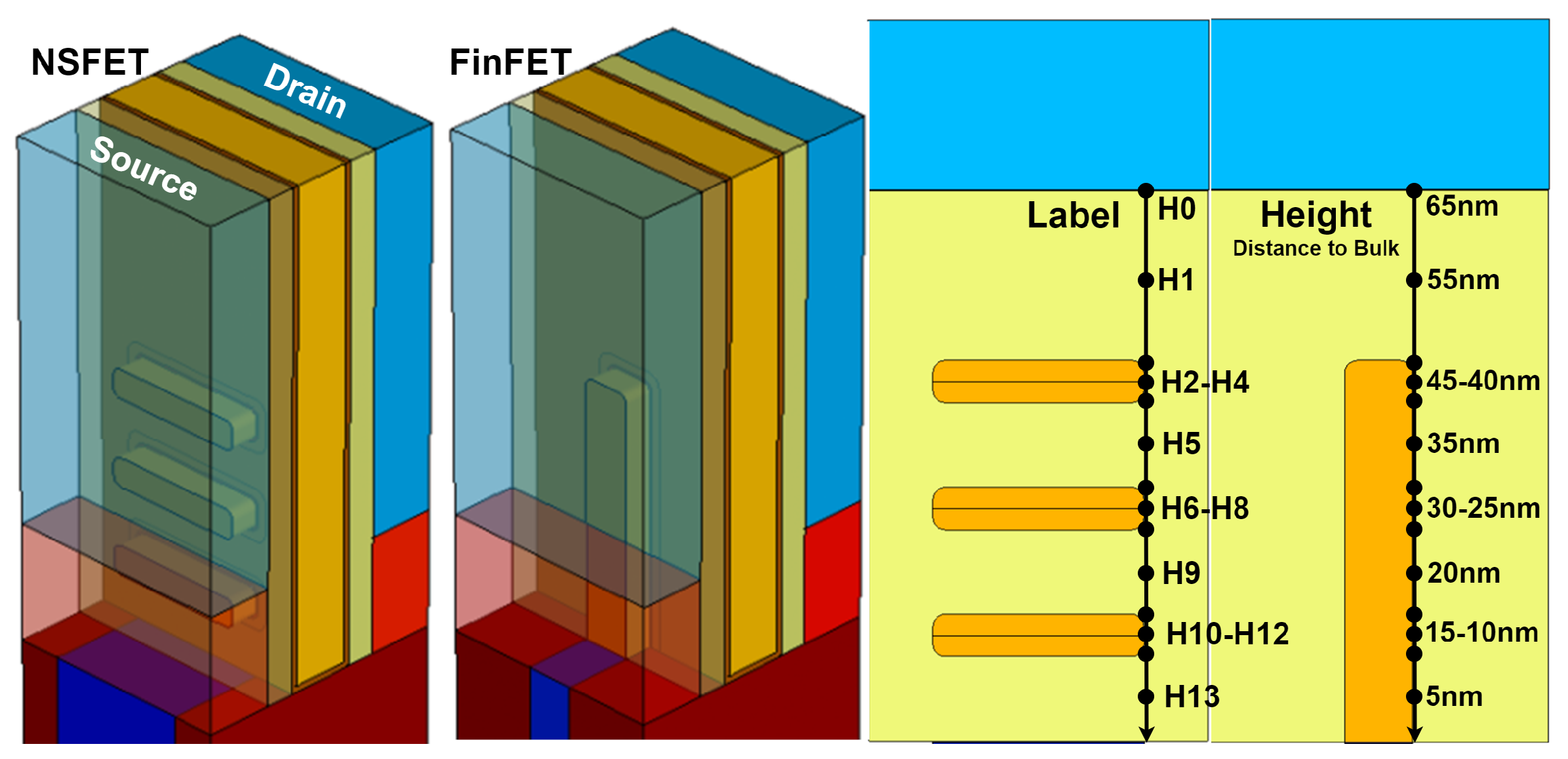
2. Device Structure and Simulation Condition

Figure 1a shows the structures of NSFET and FinFET devices used in this work. Furthermore, Figure 1b shows the channel profile and doping of the devices. As can be seen from the images, in this study, the NSFET consists of three stacked nanosheets, whereas the FinFET is a single-fin device. The main parameters related to size and doping in this work are based on the 2020 International Roadmap for Devices and Systems [16], and the specific parameters are shown in Table 1. To more intuitively and accurately compare the electrical performance of NSFET and FinFET as the source/drain height varies, the channel dimensions of FinFET were finely adjusted so that the channel areas of both devices are approximately the same, as shown in Table 2.
Simulation is performed in Sentaurus TCAD. Quantum confinement is considered by adopting the density gradient quantization model. The simulations employ the inversion layer and accumulation layer mobility models to simulate the mobility degradation caused by impurity, phonon, and surface roughness scattering. SRH recombination, Auger recombination, and the Philips unified mobility model are also adopted. Self-heating effects are considered in this simulation work, and the thermal conductivity of different regions is set according to the literature references [17]. The channel crystal orientation is precisely set, and the anisotropy of heat propagation is taken into account. Additionally, for Schottky contacts affected by lower source/drain heights, the SRDoping model is activated to consider the image-force potential lowering effect in Schottky contacts. To ensure the accuracy of the TCAD simulation, the physical model and material parameters are calibrated using NSFET experimental data [16]. The calibration results of NSFET are shown in Figure 2a and the electrical performance of FinFET under the same simulation settings are shown in Figure 2b. The simulation results in Figure 2b indicate that the electrical performance of NSFETs is significantly superior to that of FinFETs, which is consistent with the conclusions presented in other papers [3,18].

3. The Impact of Source/Drain Height Variations on Electrical Performance

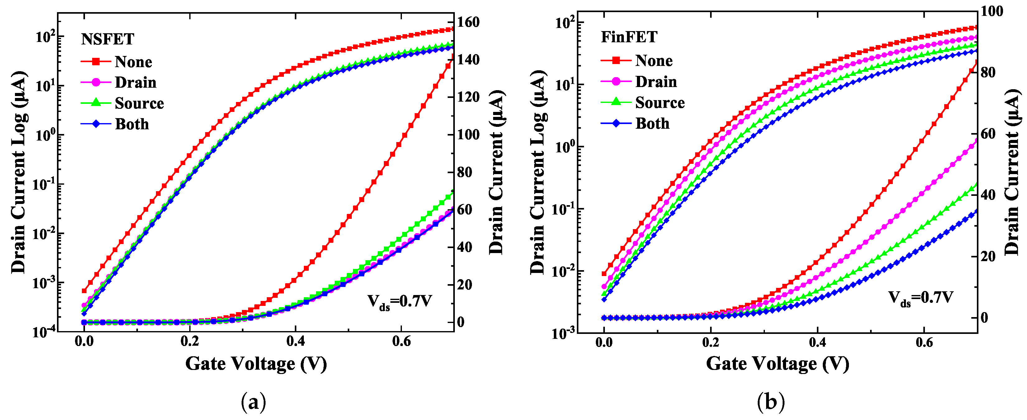
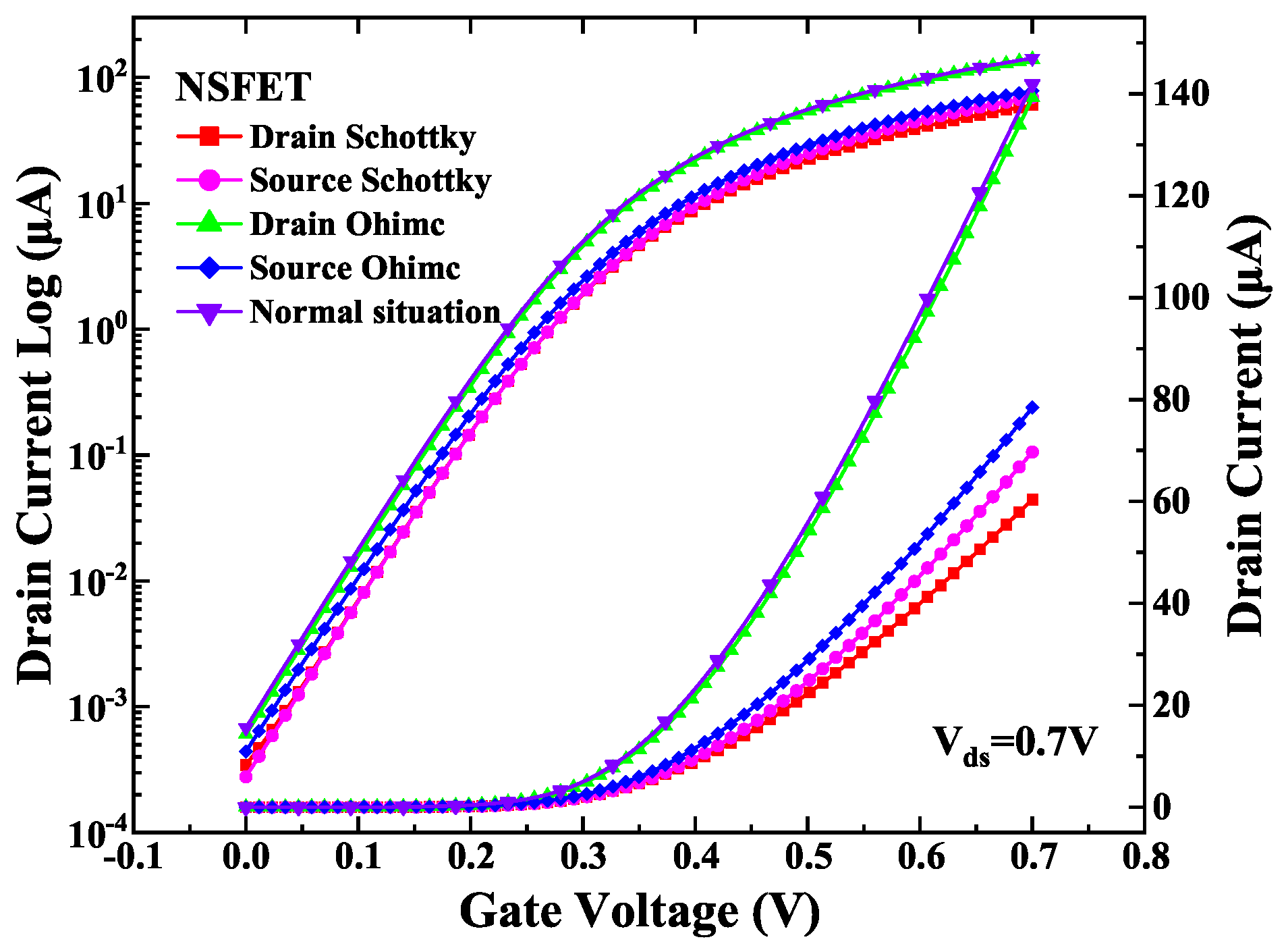
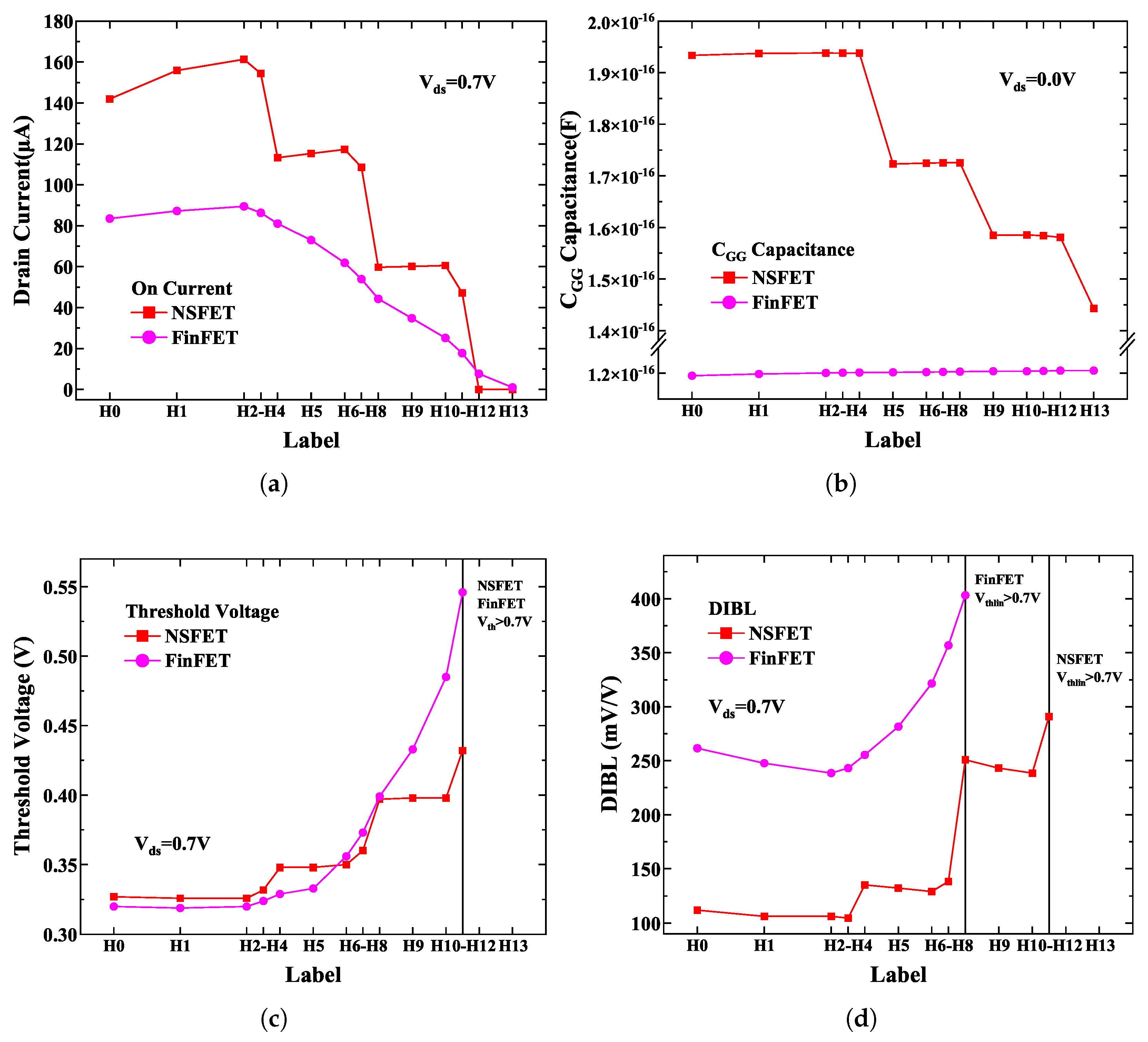
3.1. The Impact of Height Variations of Different Electrodes on Device Electrical Characteristics

Height variations in the source/drain regions caused by etching or epitaxial growth process deviations lead to electrode metal deposition over the abnormal areas during the subsequent processing steps, resulting in direct contact with the LDD region, as depicted in Figure 3. It should be noted that due to the low doping concentration in the LDD region, the contact resistance between the metal and the LDD region is the Schottky contact resistance rather than ohmic contact resistance. In this section, to thoroughly investigate the impact of height variations in different electrodes on the electrical characteristics of the devices, comprehensive simulations were conducted for FinFET and NSFET devices under conditions of abnormal source, abnormal drain, and concurrent abnormalities in both source and drain. Additionally, to significantly compare the changes in electrical characteristics between NSFET and FinFET devices, in this section, the height of the source/drain is set at the midpoint between the two lowermost nanosheets of the NSFET.
The electrical behavior of NSFET and FinFET devices with reduced source/drain heights is shown in Figure 4a,b. It can be observed from the figures that the primary impact of reduced source/drain heights on device performance is a reduction in ON-state current. When the source/drain heights are both reduced, the ON-state currents of NSFET and FinFET decrease to 49.1% and 69.3% of their original values, respectively.
However, in cases where only the source or drain is affected, the electrical properties of NSFET and FinFET show significant differences. For FinFET, the excessive etching or insufficient epitaxy of only the source has a more profound impact, whereas for NSFET, the situation is reversed. The cause of this phenomenon lies in the unidirectional conduction characteristics of the Schottky barrier. For NSFET, due to the independence of each nanosheet, the Schottky contact resistance between the drain and the LDD region impedes current flow. In contrast, for FinFET, since its channel is integrated, electrons can move through the remaining drain region; thus, the Schottky resistance at the drain has a limited obstructive effect. Additionally, this explains why the electrical characteristic curves of NSFET remain similar whether only the drain is affected or whether both the source and drain are compromised. However, if the doping concentration in the LDD region is sufficient and the contact resistance formed with the metal is ohmic, the ON-state current of NSFET with only the source dimension reduced is significantly lower than that with only the drain dimension reduced. This observation is consistent with the behavior seen in FinFET, where the current is generally higher when the source height is reduced compared to when the drain height is reduced, thereby substantiating the conclusion depicted in Figure 5. Furthermore, the simulation results in Figure 5 indicate that increasing the doping concentration in the lightly doped region to form an Ohmic contact with the metal can effectively mitigate the degradation of device performance caused by the reduction in source/drain height.
Under specific source and drain anomalies, Figure 6 exhibits the eDensity distribution for NSFET and FinFET. The figure distinctly demonstrates that any irregularities in the source and drain markedly influence the eDensity, with the source having a more pronounced impact. It is important to note that for NSFET, under Schottky contact conditions, although the eDensity is significantly higher when only the source is affected compared to when only the drain is affected, the actual ON-state current exhibits the opposite trend. This further corroborates the simulation results and related inferences presented in Figure 4 and Figure 5.
The capacitance characteristics of NSFET and FinFET devices under height variations in different electrodes are shown in Figure 7. To facilitate the understanding of the proportion of C GD and C GS within C GG , these are plotted alongside C GG on the same graph. As observed in Figure 7, when there is a change in height of only one electrode, the contact between the metal and LDD alters the electric field distribution within the channel. Consequently, both NSFET and FinFET exhibit a decrease in capacitance between the defective electrode and the gate, while the capacitance on the opposite side increases. However, the changes in capacitance characteristics on both sides counterbalance each other, resulting in minimal variation in the C GG - V G curve. In contrast, in scenarios where both the source and drain electrodes undergo height alterations, there are significant differences in the performance of NSFET and FinFET. Particularly for NSFET, the C GG shows a noticeable decrease when such defects are present. This is because the channels in NSFET are independent of each other, and the complete contact of the upper two channels with the metal significantly changes the internal electric field. For FinFET, the Schottky barrier alters the electric field of the FinFET channel, causing shifts in C GS and C GD compared to the defect-free condition. However, the overall integrity of the channel in FinFET prevents significant changes in C GG , resulting in only a slight increase in C GG .

3.2. The Impact of Varying Degrees of Height Changes on Device Electrical Characteristics

This chapter investigates the impact of varying degrees of source/drain dimension reduction caused by process fluctuations and deviations on the electrical characteristics of devices. Based on the structural characteristics of NSFET, this study selects several typical height values to examine the impact of various height changes on device electrical performance. For comparison, the same height settings were applied to FinFET, as shown in Figure 8. Additionally, to facilitate the discussion, this chapter exclusively considers scenarios where both the source and drain dimensions undergo height changes.
Under the conditions of V D = V G = 0.7 V, the relationship between the ON-state current, C GG capacitance and the degree of height reductions in the source/drain dimensions for NSFET and FinFET is illustrated in Figure 9a,b. In addition to the ON-state current and parasitic capacitance, to more thoroughly analyze the impact of reducing source/drain height on the performance of NSFET and FinFET, the threshold voltage of the devices was also extracted and the DIBL effect of the devices was calculated, as shown in Figure 9c,d. The drain bias voltage for the other transfer characteristic curve used to calculate the DIBL effect is 0.05 V. The detailed performance data of the devices, including the ON-state current, is shown in Table 3. The parts marked with “×” in the table indicate that under these conditions, with a drain bias voltage of 0.05 V or 0.7 V, the threshold voltage of the transfer characteristic curve has already exceeded 0.7 V.
From Figure 9a, it can be observed that, for NSFET, the ON-state current exhibits an increasing trend as the source/drain dimensions decrease before reaching the top nanosheet, due to the decrease in vertical resistance. When the etching defect extends into the top nanosheet, the current begins to decrease. However, as mentioned in the previous chapter, the remaining parts of the source and drain that are in contact with the LDD can still provide a current path, making the decrease in current less significant. Once the LDD region is entirely in contact with the metal, the Schottky resistance greatly inhibits the current, leading to a noticeable drop. As the degree of etching caused by process deviations increases, this process will repeat, with the ON-state current showing alternating increases and decreases. Overall, there will be a significant reduction until the entire LDD region is in contact with the metal, at which point the ON-state current is almost completely suppressed. The current variation in FinFET devices is relatively straightforward. Before the abnormal etching reaches the channel height, the ON-state current gradually increases due to the reduction in vertical resistance. Subsequently, as the source/drain dimensions continue to decrease, the current gradually decreases. Since the remaining source/drain regions in contact with the LDD always provide a current path, the final ON-state current is more significant compared to NSFET.
As for the capacitance, as mentioned in the previous chapter, due to the independence of the channels in NSFET, once the LDD region is entirely in contact with the metal, the resulting electric field change will cause a significant reduction in the C GG capacitance. In contrast, the capacitance in FinFET remains almost unchanged, with only a slight increase, as shown in Figure 9b. In summary, NSFET is more sensitive to defects in the reduction of source and drain dimensions, especially when the height corresponds to the bottom of each channel. Even minor process variations can lead to significant changes in the device’s current and capacitance.
Interestingly, the behavior of threshold voltage and DIBL effect for NSFET and FinFET are the opposite to those of the current and capacitance characteristics. As the source/drain height decreases, the changes in threshold voltage and DIBL effect for FinFET devices are much greater than those for NSFET devices. Besides the inherently better related performance characteristics of NSFET itself, the independent nature of the nanowires in NSFETs might offer some advantages. As mentioned earlier, when the drain height decreases, the Schottky barrier contact causes the nanowire to be completely turned off, almost entirely nullifying its effect of the device current. In other words, at this point, a three-stack NSFET would behave more like a two-stack NSFET or a one-stack NSFET. In contrast, for FinFET, as its channel is an integral whole, the continuously invading metal material causes the gate’s control over the upper part of the channel to weaken, eventually leading to greater fluctuations in the threshold voltage and DIBL effect.

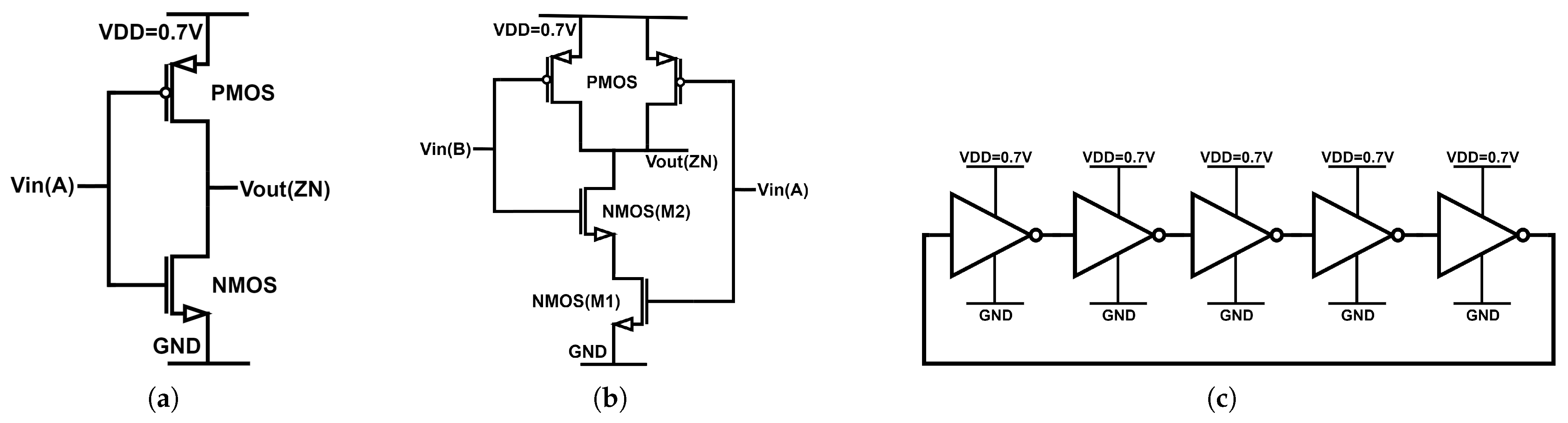
4. Circuit-Level Benchmark Results

Based on the calibration data in Figure 2, a PMOS transistor was constructed in TCAD to ensure that its ON-state current closely matches the NMOS data, as shown in Figure 10. After obtaining the electrical characteristics of the PMOS, the KeySight MBP parameter extraction software was used to extract the SPICE characteristic parameters for both NMOS and PMOS, which will be used for the subsequent cell-level simulations. Considering the structural characteristics of NSFET and the variations in ON-state current, the current characteristic curves of NSFET at 35 nm (H5), 25 nm (H9), and 5 nm (H13) were selected from Table 3 as the representative values. These values were used to simulate the circuit performance of NSFET under different conditions of channel failure. Additionally, due to the significant difference in the magnitude of the ON-state current between defect levels of 25 nm (H9) and 5 nm (H13) in NSFET, cases with defect levels of 10 nm (H12) and 5 nm (H13) in FinFET were also selected to simulate the device’s performance under severe defects without complete failure (open circuit), caused by process deviations. For convenience, in the following text, the NMOS transistors are sorted in descending order of their ON-state currents and relabeled from Case 0 to Case 5, as shown in Table 4.
In this study, NMOS and PMOS transistors were utilized to construct basic inverter cells, two-input NAND gates, and a five-stage ring oscillator, as shown in Figure 11. Subsequently, the internal NMOS transistors were replaced with transistors of different source/drain heights to study the impact of source/drain height variations caused by process deviations on cell-level circuit performance. The output voltage under DC simulation settings for the inverter (INV) is presented in Table 5, the output voltage under DC simulation settings for the NAND gate is shown in Table 6, and the delay data for the five-stage ring oscillator, under various conditions, is detailed in Table 7. It is important to note that test results demonstrate no significant delay changes when the five NMOS transistors in the ring oscillator are sequentially replaced with transistors of varying source/drain heights. Therefore, Table 7 displays only the average values. Additionally, the influence of parasitic parameters at the 7 nm process node was also considered in the simulation.
The DC simulation results for the inverter, as presented in Table 5, demonstrate that minor variations in current caused by height reduction do not impact the output voltage. However, as the severity of transistor defects increases, the deviation of the output voltage from the standard value also rises. When the ON-state current decreases by 95% (7.7 μ A), a noticeable shift in the output voltage is observed. Furthermore, when the ON-state current reduction exceeds 99% (1.0 μ A), the voltage offset surpasses 60%, leading to the failure of the inverter’s logical function. The simulation results for the NAND gate in Table 6 are similar to those for the inverter, though the overall trend is more gradual. Additionally, the simulation results indicate that the impact is more severe for transistors near the NAND gate output under the same defect conditions. The data in Table 7 indicate that the delay of the ring oscillator increases as the current decreases. When the current variation is minor, the ring oscillator does not generally experience functional failure. However, when the ON-state current decreases by 95% (7.7 μ A), functional failure occurs at a lower bias voltage (0.5 V), while at a higher bias voltage (0.7 V), its basic function can still be maintained but with extremely high delay. When the ON-state current reduction exceeds 99% (1.0 μ A), the functionality of a single inverter can no longer be sustained, leading to the functional failure of the five-stage ring oscillator.

5. Conclusions

This paper investigates the impact of process fluctuations and deviations in etching and epitaxial growth before the metal material deposition on the performance of NSFET and FinFET devices, providing a reliable basis for subsequent improvements in source/drain process detection. The results indicate that for both NSFET and FinFET, a reduction in the height of the source or drain leads to a decrease in the ON-state current, thereby affecting device performance. Notably, unlike FinFET, the individual nanosheets in NSFET are independent. When a nanosheet comes into complete contact with the metal, the Schottky resistance significantly obstructs the current flow within that nanosheet. Similarly, due to the independence of different channels in NSFETs, the Schottky barrier significantly alters the electric field distribution within the channels, resulting in a significant reduction in the capacitance of NSFET. Therefore, NSFET are more sensitive to changes in etching and epitaxial growth processes, making these processes critical factors in the manufacturing of NSFET as next-generation semiconductor devices. However, NSFET does not show higher sensitivity across all performance parameters. Compared to FinFET, NSFET shows better resistance to the threshold voltage and drain-induced barrier lowering (DIBL) effect. Additionally, the simulations of the INV cell, NAND cell, and ring oscillator indicate that the reduction in source/drain height leads to a gradual transition from defect-free functionality to hard defects. This specific performance is closely related to conditions such as bias voltage and transistor position. Therefore, in circuit-level defect diagnostics, it is also necessary to comprehensively consider factors such as the circuit structure and bias conditions to account for this scenario.

Author Contributions

Conceptualization, M.M., C.L. and M.J.D.; Funding acquisition, C.L. and H.Y.; Investigation, M.M.; Methodology, M.M.; Software, M.M., J.M., W.Y. and H.L.; Supervision, C.L. and H.Y.; Validation, M.M.; Writing—review and editing, M.M., C.L. and M.J.D. All authors have read and agreed to the published version of the manuscript.

Funding

This work was supported by the National Key Research and Development Program of China: Research on Industrial Analog Chip Designs and Process Compatibility and Standards for Reliability Technologies (Grant No. 2022YFF0605800).

Data Availability Statement

Data are contained within the article.

Conflicts of Interest

The authors declare no conflicts of interest. This paper reflects the views of the scientist and not those of the company or institute.

References

  1. Xie, Q.; Lin, X.; Wang, Y.; Dousti, M.J.; Shafaei, A.; Ghasemi-Gol, M.; Pedram, M. 5 nm FinFET Standard Cell Library Optimization and Circuit Synthesis in Near-and Super-Threshold Voltage Regimes. In Proceedings of the 2014 IEEE Computer Society Annual Symposium on VLSI, Tampa, FL, USA, 9–11 July 2014; IEEE: Piscataway, NJ, USA, 2014; pp. 424–429. [Google Scholar]
  2. Mertens, H.; Ritzenthaler, R.; Hikavyy, A.; Kim, M.S.; Tao, Z.; Wostyn, K.; Chew, S.A.; De Keersgieter, A.; Mannaert, G.; Rosseel, E.; et al. Gate-all-around mosfets based on vertically stacked horizontal si nanowires in a replacement metal gate process on bulk si substrates. In Proceedings of the 2016 IEEE Symposium on VLSI Technology, Pittsburgh, PA, USA, 11–13 July 2016; IEEE: Piscataway, NJ, USA, 2016; pp. 1–2. [Google Scholar]
  3. Loubet, N.; Hook, T.; Montanini, P.; Yeung, C.W.; Kanakasabapathy, S.; Guillom, M.; Yamashita, T.; Zhang, J.; Miao, X.; Wang, J.; et al. 5 nm FinFET Stacked nanosheet gate-all-around transistor to enable scaling beyond finfet. In Proceedings of the 2017 Symposium on VLSI Technology, Kyoto, Japan, 5–8 June 2017; IEEE: Piscataway, NJ, USA, 2017; pp. T230–T231. [Google Scholar]
  4. Champac, V.; Garcia Gervacio, J.; Champac, V.; Garcia Gervacio, J. Designing with FinFETs and Process Variation Impact. In Timing Performance of Nanometer Digital Circuits Under Process Variations; Springer: Berlin/Heidelberg, Germany, 2018; pp. 143–163. [Google Scholar]
  5. Pande, N.; Zhou, C.; Lin, M.H.; Fung, R.; Wong, R.; Wen, S.; Kim, C.H. Characterizing electromigration effects in a 16 nm FinFET process using a circuit based test vehicle. In Proceedings of the 2019 IEEE International Electron Devices Meeting (IEDM), San Francisco, CA, USA, 7–11 December 2019; IEEE: Piscataway, NJ, USA, 2019; pp. 5.3.1–5.3.4. [Google Scholar]
  6. Kumari, N.A.; Prithvi, P. Performance evaluation of GAA nanosheet FET with varied geometrical and process parameters. Silicon 2022, 14, 9821–9831. [Google Scholar] [CrossRef]
  7. Kim, S.; Lee, K.; Kim, S.; Kim, M.; Lee, J.H.; Kim, S.; Park, B.G. Investigation of device performance for fin angle optimization in FinFET and gate-all-around FETs for 3 nm-node and beyond. IEEE Trans. Electron. Devices 2022, 69, 2088–2093. [Google Scholar] [CrossRef]
  8. Kim, S.; Kim, M.; Ryu, D.; Lee, K.; Kim, S.; Lee, J.; Lee, R.; Kim, S.; Lee, J.H.; Park, B.G. Investigation of electrical characteristic behavior induced by channel-release process in stacked nanosheet gate-all-around MOSFETs. IEEE Trans. Electron. Devices 2020, 34, 2648–2652. [Google Scholar] [CrossRef]
  9. Wei, T.C.; Narang, V.; Thean, A. Electrical characterization of FEOL bridge defects in advanced nanoscale devices using TCAD simulations. In Proceedings of the 2018 IEEE International Symposium on the Physical and Failure Analysis of Integrated Circuits (IPFA), Singapore, 16–19 July 2018; pp. 1–4. [Google Scholar]
  10. Dibaj, R.; Al-Khalili, D.; Shams, M. Gate Oxide Short Defect Model in FinFETs. J. Electron. Test. 2018, 34, 351–362. [Google Scholar] [CrossRef]
  11. Bhat, T.S.; Shintri, S.; Chen, B.; Lo, H.C.; Peng, J.; Qi, Y.; Willeman, M.; Mishra, S.K.; Yuksek, N.; Gao, W.Z. Abnormal silicon-germanium (SiGe) epitaxial growth in FinFETs. IEEE Trans. Semicond. Manuf. 2020, 33, 291–294. [Google Scholar] [CrossRef]
  12. Li, X.; Dube, A.; Ye, Z.; Sharma, S.; Kim, Y.; Chu, S. Selective epitaxial Si: P film for nMOSFET application: High phosphorous concentration and high tensile strain. ECS Trans. 2018, 64, 959. [Google Scholar] [CrossRef]
  13. Wang, Y.; Zheng, S.; Zhang, S.; Wang, J.; Lu, G.; Wen, G. Study on Different Failure Mechanisms of MOSFET Caused by Different Oxide Defects in 14 nm FinFET IC. In Proceedings of the 2024 IEEE International Symposium on the Physical and Failure Analysis of Integrated Circuits (IPFA), Singapore, 15–18 July 2024; pp. 1–4. [Google Scholar]
  14. Wang, D.; Sun, X.; Liu, T.; Chen, K.; Yang, J.; Wu, C.; Xu, M.; Zhang, W. Investigation of Source/Drain Recess Engineering and Its Impacts on FinFET and GAA Nanosheet FET at 5 nm Node. Electronics 2023, 12, 770. [Google Scholar] [CrossRef]
  15. Pelosi, M. From FinFET to Nanosheet Si-SiGe GAAFET: Fabrication Process Simulation and Analysis. Ph.D. Thesis, Politecnico di Torino, Turin, Italy, 2021. [Google Scholar]
  16. International Roadmap for Devices and Systems More Moore. 2020. Available online: https://irds.ieee.org/editions/2020 (accessed on 1 March 2025).
  17. Tsen, C.J.; Chung, C.C.; Liu, C.W. Self-heating mitigation of treefets by interbridges. IEEE Trans. Electron. Devices 2022, 69, 4123–4128. [Google Scholar] [CrossRef]
  18. Mertens, H.; Ritzenthaler, R.; Pena, V.; Santoro, G.; Kenis, K.; Schulze, A.; Litta, E.D.; Chew, S.A.; Devriendt, K.; Demuynck, S.; et al. Vertically stacked gate-all-around si nanowire transistors: Key process optimizations and ring oscillator demonstration. In Proceedings of the 2017 IEEE International Electron Devices Meeting (IEDM), San Francisco, CA, USA, 2–6 December 2017; pp. 37.4.1–37.4.4. [Google Scholar]
Figure 1. (a) Structure of 3-stack NSFET and FinFET (Cutline A-A), (b) Doping of 3-stack NSFET and FinFET (Cutline B-B).
Electronics 14 01091 g001
Figure 2. (a) TCAD calibration results (line) and the experimental data (symbols) for NSFET. (b) I D - V G curves of NSFET and FinFET under the same settings.
Electronics 14 01091 g002
Figure 3. Height variations in the source/drain regions. From left to right: no variation, variation in the drain, variation in the source, and variation in both the source and drain.
Electronics 14 01091 g003
Figure 4. (a) I D - V G curves of NSFET under height variations in different electrodes. (b) I D - V G curves of FinFET under height variations in different electrodes.
Electronics 14 01091 g004
Figure 5. I D - V G curves with different contact resistances under changes in height of only the source or the drain.
Electronics 14 01091 g005
Figure 6. eDensity distribution in NSFET and FinFET under height variations in different electrodes.
Electronics 14 01091 g006
Figure 7. (a) C GD - V G and C GG - V G curves of NSFET under height variations in different electrodes. (b) C GD - V G and C GG - V G curves of FinFET under height variations in different electrodes. (c) C GS - V G and C GG - V G curves of NSFET under height variations in different electrodes. (d) C GS - V G and C GG - V G curves of FinFET under height variations in different electrodes.
Electronics 14 01091 g007
Figure 8. Extent of metal intrusion in the source and drain under different process variations.
Electronics 14 01091 g008
Figure 9. (a) Comparison of ON-state current in NSFET and FinFET at different source/drain heights. (b) Comparison of C GG capacitance in NSFET and FinFET at different source/drain heights. (c) Comparison of threshold voltage in NSFET and FinFET at different source/drain heights. (d) Comparison of DIBL in NSFET and FinFET at different source/drain heights.
Electronics 14 01091 g009
Figure 10. I D - V G characteristics of PMOS for the circuit-level simulation.
Electronics 14 01091 g010
Figure 11. (a) INV circuit schematic. (b) NAND circuit schematic. (c) 5-stage RO circuit schematic.
Electronics 14 01091 g011
Table 1. Device physics parameters.
ParameterSymbolValue
Gate Length L g 12 nm
Spacer Length L sp 5 nm
Inner Spacer Length L insp 1 nm
S/D Length L sd 12 nm
S/D Height H sd 65 nm
Nano-Sheet Width NS W 25 nm
Nano-Sheet Thickness NS T 5 nm
Nano-Sheet Distance NS D 10 nm
Fin Width Fin W 8.3 nm
Fin Height Fin H 45 nm
Equivalent Oxide Thickness E OT 0.7 nm
Channel Doping N Ch 1 × 10 16 cm 3
LDD Doping N LDD 2 × 10 18 cm 3
S/D Doping N SD 2 × 10 20 cm 3
Bulk Doping N Bulk 2 × 10 18 cm 3
Substrate Doping N Sub 2 × 10 18 cm 3
Gate Work Function W F 4.41 eV
Table 2. Effective channel area of NSFET and FinFET.
Device TypesFormulaValue
NSFET NS W × NS T × 3 375 nm 2
FinFET Fin W × Fin H 373.5 nm 2
Table 3. Electrical characteristic data of NSFET and FinFET at different source/drain heights.
Label H sd  (nm) I on  ( μ A) C GG ( 10 16 F) V th  (V)DIBL (mV/V)
NSFETFinFETNSFETFinFETNSFETFinFETNSFETFinFET
H065.0141.9583.511.9341.1950.3270.320112.0261.5
H155.0155.8887.211.9371.1990.3260.319106.2247.7
H245.0161.3089.481.9381.2010.3260.320106.2238.5
H342.5154.3986.351.9381.2010.3320.324104.6243.1
H440.0113.2681.041.9381.2010.3480.329135.4255.4
H535.0115.3273.001.7231.2020.3480.333132.3281.5
H630.0117.2961.891.7251.2020.3500.356129.2321.5
H727.5108.6053.951.7251.2030.3600.373138.5356.9
H825.059.7644.331.7261.2030.3970.399250.8403.1
H920.060.1334.851.5851.2040.3980.433243.1×
H1015.060.6025.201.5851.2040.3980.485238.5×
H1112.547.2217.751.5841.2040.4320.546290.8×
H1210.0 8 × 10 5 7.711.5811.205××××
H135.0 6 × 10 5 1.011.4431.205××××
Table 4. Data of NMOS transistors for circuit simulation.
LabelCase 0Case 1Case 2Case 3Case 4Case 5
Device TypeNSFETNSFETNSFETFinFetFinFetNSFET
Height (nm)65 (H0)35 (H5)20 (H9)10 (H12)5 (H13)5 (H13)
On Current ( μ A)141.9115.360.17.71.0 6.20 × 10 5
Table 5. Output voltage values and voltage offsets of inverters under different conditions.
Cell: INV V DD = 0.7 V
LabelOn Current ( μ A) V A  (V) V ZN  (V)Voltage Offect
Case 0141.90.7000
Case 1115.30.7000
Case 260.10.7000
Case 37.70.700.122917.6%
Case 41.00.700.641991.7%
Case 5 6.20 × 10 5 0.700.698599.8%
Table 6. Output voltage values and voltage offsets of NAND under different conditions.
Cell: NAND V DD = 0.7 V
LabelOn Current ( μ A) V A & V B  (V) V ZN  (V)Voltage Offect
Case 0 (M1)141.90.700.00590.8%
Case 1 (M1)115.30.700.00851.2%
Case 2 (M1)60.10.700.06959.9%
Case 3 (M1)7.70.700.242934.7%
Case 4 (M1)1.00.700.598785.5%
Case 5 (M1) 6.20 × 10 5 0.700.696199.4%
Case 0 (M2)141.90.700.00580.8%
Case 1 (M2)115.30.700.01462.1%
Case 2 (M2)60.10.700.071110.2%
Case 3 (M2)7.70.700.264837.8%
Case 4 (M2)1.00.700.599185.6%
Case 5 (M2) 6.20 × 10 5 0.700.696299.4%
Table 7. Delay of the 5-stage RO at VDD = 0.5 V/0.7 V under different conditions.
Cell: 5-Stage RO V DD = 0.5/0.7 V
LabelOn Current ( μ A)0.5 V T Delay  (ps)0.7 V T Delay  (ps)
Case 0141.98.325.94
Case 1115.38.956.42
Case 260.111.27.53
Case 37.7Functional Failure10.57
Case 41.0Functional FailureFunctional Failure
Case 5 6.20 × 10 5 Functional FailureFunctional Failure
Disclaimer/Publisher’s Note: The statements, opinions and data contained in all publications are solely those of the individual author(s) and contributor(s) and not of MDPI and/or the editor(s). MDPI and/or the editor(s) disclaim responsibility for any injury to people or property resulting from any ideas, methods, instructions or products referred to in the content.

