Article

A Comprehensive Numerical Analysis of a 2.45 GHz Energy Harvesting Rectenna System and a Proposal for a Figure of Merit for Rectenna Systems †

1
Aix Marseille Université, CNRS, Université de Toulon, IM2NP UMR 7334, 13397 Marseille, France
2
Faculty of Science, Lebanese University, Beirut 6573, Lebanon
3
Independent Researcher, Dubai 54339, United Arab Emirates
*
Authors to whom correspondence should be addressed.
This article contains a revised version of a paper entitled “Low power CMOS bridge Rectenna”, which was presented at IEEE Conference on Antenna Measurements and Applications (CAMA), Guangzhou, China, 2022, Additionally, an extended version of “2.45 GHz Low-Power Diode Bridge Rectifier Design”, which was presented at International Conference on Microelectronics (ICM), Abu Dhabi, United Arabe Emirates, 2023.
Electronics 2025, 14(4), 716; https://doi.org/10.3390/electronics14040716
Submission received: 14 November 2024 / Revised: 17 January 2025 / Accepted: 7 February 2025 / Published: 12 February 2025
(This article belongs to the Special Issue RF/MM-Wave Circuits Design and Applications, 2nd Edition)

Abstract

:
This work presents a numerical analysis of a 2.45 GHz full-wave bridge rectifier for RF (radio frequency) energy harvesting under low-power input conditions, and a guideline for developing a figure of merit (FOM) for RF energy harvester rectennas by relying on data science techniques, laying the foundation for a universally accepted FOM. The performance of the full-wave bridge rectifier, using two types of Schottky diodes, HSMS2850 and SMS7630, was evaluated at −5 and −15 dBm, with the diodes achieving maximum power conversion efficiencies (PCEs) of 57% and 33%, respectively, and reflection coefficient S11 values below −30 dB. A printed circuit board was designed to prepare for future laboratory measurements offering insights into real-world performance. Additionally, a double-voltage rectifier was simulated, achieving PCE values of 41% and 66% at similar input power levels; furthermore, various CMOS-based rectifier topologies reached PCE values of 69% at −5 dBm and 43.6% at −26 dBm.

1. Introduction

In the 1870s, Karl Ferdinand Braun observed asymmetrical conduction in crystals such as galena, enabling current to flow preferentially in one direction. His study [1] is considered the first systematic exploration of metal–semiconductor contacts.
In 1904, John Ambrose Fleming invented the thermionic vacuum tube, or oscillation valve, patented on 16 November [2]. Known as the Fleming valve, it marked a key development in early electronics.
In the 1920s, selenium devices gained widespread use in applications such as photographic exposure meters and rectifiers [3]. Prior to the emergence of silicon and germanium [4] rectifiers, selenium was regarded as one of the most significant materials in the semiconductor industry.
By offering better high-frequency performance, these developments ushered in the solid-state era, gradually displacing vacuum tubes in radios and other applications.
The 1950s saw the rise of silicon diodes with superior thermal performance to germanium. Schottky diodes, with a low voltage drop and fast switching, emerged in the late 1950s [4], revolutionizing high-frequency signal detection and power conversion, paving the way for integrated microwave circuits in the following decades.
The growing demand for sustainable energy solutions has increased the interest in wireless power transmission, a field that originated with the development of rectenna (rectifying antenna) circuits in the 1960s, which were designed to convert microwave energy into direct current (DC) [5].
Nowadays, due to the adoption of RF transmitters in Wi-Fi, cellular networks, and other communication technologies, ambient RF energy levels have significantly increased, especially in urban areas. Although Wi-Fi signals provide relatively low power, they are suitable for harvesting for a wide range of applications in smart cities, for example, for the power supply of low-power sensors that monitor environmental conditions such as air quality, temperature, and humidity. In healthcare, low-power devices such as implantable sensors and wearable health monitors can utilize ambient RF energy to extend their battery life. Overall, RF energy harvesting enhances user convenience, lowers maintenance costs, reduces electronic waste, and supports sustainable development goals.
A rectenna system typically consists of five core components (Figure 1): an antenna; impedance matching; filters to eliminate, if any, unwanted direct current (DC) and alternative current (AC) signals that could potentially disrupt the functionality of the bridge elements; a full-wave bridge rectifier; and a voltage regulator that stabilizes the converted signal, transforming it into a DC signal.
The majority of recent works have focused on enhancing rectifier performance by utilizing relatively higher input power (Pin), with fewer studies exploring performance at lower power levels. Various studies have reported power conversion efficiencies (PCEs) across a range of input power levels. At a higher input power, Ref. [6] achieved a PCE of 91% at 37 dBm, while [7] reported 75% at 27 dBm, and [8] achieved 77% at 15 dBm. As the input power decreased to 13 dBm and 6 dBm, Refs. [9,10] recorded PCEs of 81% and 45%, respectively. At lower input levels, Refs. [11,12] achieved PCEs of 70% at 5 dBm and 74% at 3.5 dBm, while [13] obtained 47% at 1 dBm. Below 1 dBm, Ref. [14] recorded 52% at 0.8 dBm, and [15] observed 30% at 0 dBm. At negative input power levels, Ref. [16] achieved 48% at −3 dBm, while [10,17] reported 41% and 20% at −5 dBm and −6 dBm, respectively. For even lower levels, Refs. [18,19] recorded 35% and 37% at −10 dBm, while [20] achieved 59% at −12 dBm, and [17] observed 27% at −15 dBm.
Our study focuses on the following two technologies: the silicon-based diodes HSMS2850 and SMS7630, known for their low turn-on voltage, and CMOS (complementary metal-oxide semiconductor) transistor technology, valued for its power consumption being lower than that of commercial diodes and its potential for higher PCE. In so doing, we aim to achieve relatively high PCEs at low power inputs with low-cost and easy-to-implement circuits. This context highlights the need for a methodology that integrates empirical data derived from simulations, laboratory measurements, and statistical analyses. Consequently, we propose an approach aimed at establishing a figure of merit (FOM) specifically tailored to evaluate the efficiency and performance of RF energy harvester rectennas.

2. Methods

This part of the document first addresses various methods for analyzing rectenna topologies. In the second part, it proposes an approach to build a figure of merit (FOM) for RF energy harvesting rectennas based on data gathering and analysis methods.

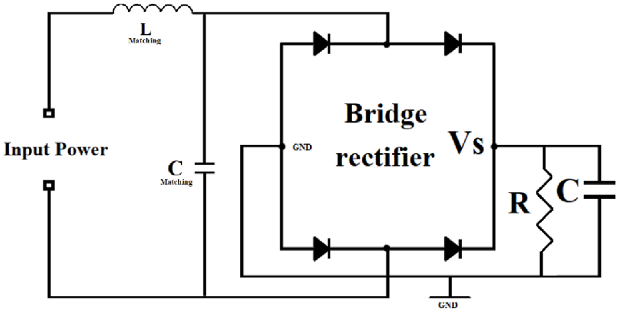
2.1. Bride Rectifier Topologies

This section addresses the rectenna topologies, including Schottky diode full-wave bridge rectifiers, which offer higher output currents and minimize parasitic ripples. It also examines voltage doublers, which provide higher output voltages, as well as CMOS rectifiers.

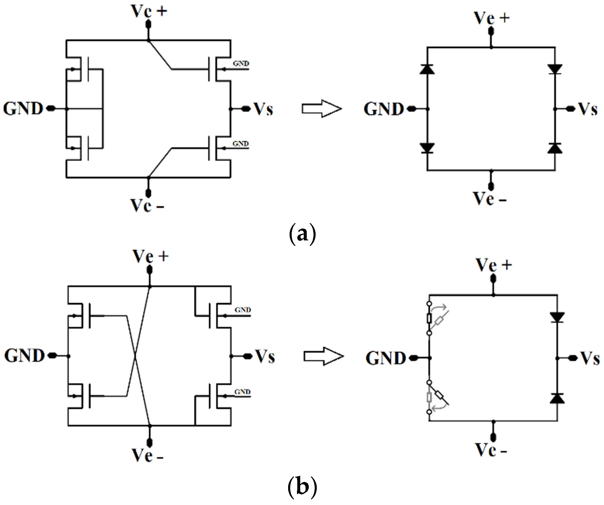
2.1.1. Schottky Diode Full-Wave Bridge Rectifier

The design and study process of the Schottky diode bridge rectifier consisted of the following steps:
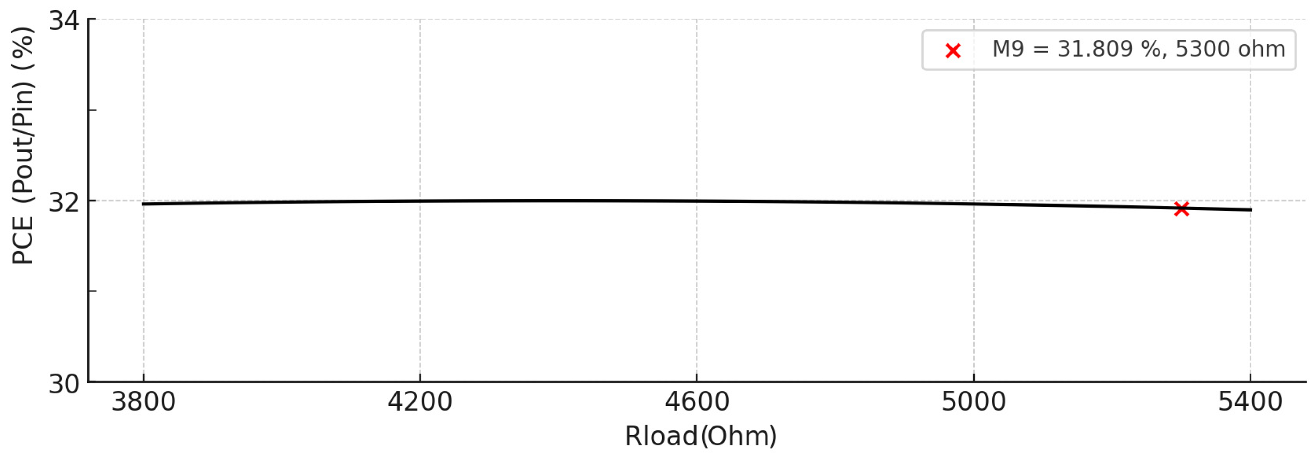
  • A simulation was conducted for a bridge rectifier configuration and voltage regulator (Figure 2). This baseline topology served to first identify the ideal R load value in order to obtain the maximum PCE (Pin/Pout). The SPICE model parameters of the HSMS2850 [21] and SMS7630 [22] diode components were incorporated by referring to their corresponding datasheets.
  • Simulations and evaluations of different impedance-matching configurations were carried out by using either discrete components or microstrip lines.
  • The bridge rectifier printed circuit board was realized.
  • A detailed theoretical calculation of the PCE (power conversion efficiency) was compared to the simulation results in order to explain and break down the power conversion phases.

2.1.2. Schottky Diode Voltage Doubler Rectifier

A simulation was performed for the voltage doubler rectifier configuration (Figure 3). The load resistor was selected to match the final value of the full-wave bridge rectifier, allowing for a comparative analysis of relative PCE. The SMS7630 diode was utilized due to its superior performance in the full-wave bridge rectifier.

2.1.3. CMOS Technology Bridge Rectifier

After evaluating the performance of the Schottky diode, we shifted our focus to exploring alternative MMIC (monolithic microwave integrated circuit) rectifier topologies that leverage CMOS technology, due to their low power consumption levels and reduced circuit dimensions.
Based on a thorough analysis, 130 nm CMOS technology was selected for its dimensional properties being suitable for targeted frequency and low-power consumption, thus maximizing the bridge rectifier’s efficiency.
The simulations included an initial phase of transistor characterization, followed by a half-wave bridge rectifier, and then a full-wave bridge rectifier. Three distinct topologies were examined for the full-wave bridge rectifier by connecting the transistor in diode and switch mode combinations.
The exploration of various rectenna designs highlights the potential of different rectifier technologies for optimizing the RF energy harvesting performance. These insights emphasize the need for a structured evaluation metric that can be used to objectively compare rectenna efficiency across diverse designs and operational conditions. To address this, the next section introduces a figure of merit framework, with the aim of establishing a standardized benchmark for assessing RF energy harvesting systems.

2.2. Figure of Merit Approach

Comparing different electronic systems with different characteristics is challenging, as it leads to a diverse set of evaluation criteria. This makes it difficult to establish a comprehensive approach for comparing performance.
The purpose of this preliminary work is to establish a foundational approach to generating an FOM, explained through six steps as follows:
  • Expert consensus and definition of comparison criteria.
  • Data collection and benchmarking.
  • Exploratory data analysis (EDA) and preprocessing.
  • Application of PCA (principal component analysis).
  • Results and loading analysis.
  • FOM development guidelines and validation.

2.2.1. Expert Consensus and Definition of Comparison Criteria

Table 1 lists the grouped criteria that have an impact on the efficiency and performance of rectenna systems. To simplify the following description of our approach, we consider each criterion as a metric named by convention as  M 1 , M 2 , , M n .

2.2.2. Data Collection and Benchmarking

The data collection step aims to identify a list of circuits with known measurements and performance outcomes. The circuit list should contain diverse operational environments, such as those with different frequencies, technologies, and topologies following the measurable criteria.
Empirical data for the above selected circuits must be gathered by using a common data collection method that is standardized as much as possible to maintain data consistency by using the same tools, environments, and settings.
These data should be classified in a matrix format, where columns represent the criteria ( M 1 , M 2 , , M 13 .), and rows represent the compared circuits, as shown in Table 2.

2.2.3. Exploratory Data Analysis and Preprocessing

The exploratory data analysis will provide a deeper understanding of the underlying structure of the dataset. It consists of the following actions:
  • Identify missing measurements or data that were impossible to collect.
  • Fill the missing data with every criterion mean, making sure not to affect their overall variance.
  • Normalize by transforming all collected data into a common scale (for example, Min–Max scaling) to mitigate the influence of variance scales in the modeling.
  • Subtract the mean of each criterion from the dataset to center the data on zero.
We then calculate a covariance matrix of the centered data resulting from step 4 to understand how metrics vary together and eliminate redundant data. For example, in our selected criteria, the covariance matrix might highlight a high correlation between the matching network efficiency (Pin/Pavailable), PCE (Pout/Pin), and power factor (Pout/Pavailable) due to their common variability.

2.2.4. Application of Principal Component Analysis

The data matrix output of the above step will be composed of “n” dimensions of comparisons (n = 13). To identify the relative importance of every criterion in the FOM, the PCA [23] helps to reduce dimensionality and identify the principal components that capture the most variance (higher impact) in the dataset.
The data matrix is split into two parts:
  • A total of 70% is used as a training panel to build the PCA model [24] (described below).
  • A total of 30% is used to validate the FOM (described in Section 2.2.6).

Eigenvalue Decomposition

Eigenvalue decomposition is a mathematical method used to break down criteria and find new key directions that summarize the most important patterns in the training dataset. This method identifies  k  eigenvectors (principal components) and their corresponding eigenvalues (explained variance) with  k  ≤ n, where n = 13 in our case (Figure 4). The principal component is a linear combination of the criteria described below:
P C i = ω j i M j
where  ω j i  are the “loadings” that represent the contribution of each original criterion to each principal component ( P C 1   t o   P C k ), as shown in Figure 5.

Dimensionality Reduction

Dimension reduction consists of selecting the principal components that represent a significant part of the dataset variance proportion (2). These principal components are selected by filtering the largest eigenvalues  λ i  until they account for 80–90% of the total eigenvalue sum ( j = 1 k λ j ).
V a r i a n c e   p r o p o r t i o n   ( P C i ) = λ i j = 1 k λ j
Following this selection, the most important patterns are captured, and some less critical information might be left out.

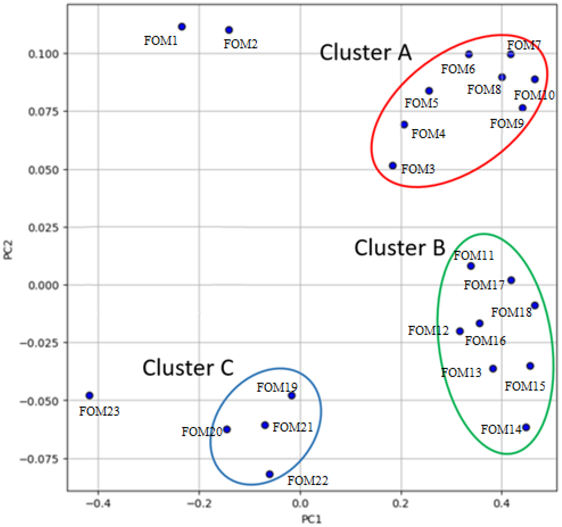
2.2.5. Results and Loading Analysis

To better understand which criteria are most critical in explaining the dataset variance, the loadings  ω j i  (contributions) of each original criterion on the selected principal components can be visualized, allowing for the accuracy of the output of the previous step (eigenvalue decomposition) to be confirmed.
A synthetic example for demonstration purposes is shown in Figure 6. The PCA attributed large loadings from  M 3 , M 4 , M 5  on PC1 compared to on PC2 (the variation along the PC1 axis is greater than that along the PC2 axis), while M7 and M8 represent the opposite.
At the end of this step, new groupings of the original criteria might emerge, differing from those identified in Table 1.

2.2.6. Figure of Merit Development Guidelines and Validation

Finally, we are able to propose an FOM based on the analysis in the previous step, as well as a validation method.

Figure of Merit Development

The principal components selected following the dimension reduction are used, and a reverse analysis is conducted to extract the measures that they explain in order to ensure that the most significant metric (Criteria M) will have the most impact on the FOM, followed by assigning a weight for each metric M based on its principal component variance proportion and loadings.
F O M s c o r e ( M 1 , , M n ) = j = 1 X λ j i = 1 n M i ω i j j = 1 X λ j
where “X” is the number of selected principal components, and “n” is the number of total criteria. Scoring normalization is performed if needed depending on the final values of  ω i j  and  λ j .

Figure of Merit Validatio

The pertinence of this new FOM needs to be validated by comparing the scores of the remaining 30% of the test panel (cf. 2.2.4) against known performance outcomes based on the expert team’s opinion.
To this end, the visual representations of the circuits on their principal components (PCA biplots), alongside their FOM scores, must show very similar FOM values for circuits within the same cluster, as shown in Figure 7.
The above-presented guidelines will help us to develop the figure of merit (FOM) by performing simulations and laboratory measurements. It is important to note that this paper is limited to a theoretical guideline proposal and does not encompass experimental validation. Future work will need to address this gap by implementing the proposed guidelines in practical applications to assess their effectiveness.

3. Results and Discussion of Rectenna System Topologies and Technologies Analysis

This part of the document presents a comparison of several full-wave bridge simulation results for low-power RF energy harvesting. Theoretical calculations and simulations of a full-wave bridge rectifier were carried out, and a printed circuit board (PCB) was designed for future laboratory measurements; additionally, a voltage doubler topology was also simulated. Both topologies were simulated using Advanced Design System (ADS). Several bridge rectifier topologies using CMOS technology were also simulated using Cadence Virtuoso 6.1.7-64b software.

3.1. Diode Bridge Rectifier

To set the context for the following sections, we begin by examining the fundamental concepts and design considerations of the diode bridge rectifier, which are pivotal for achieving optimal performance in power conversion.

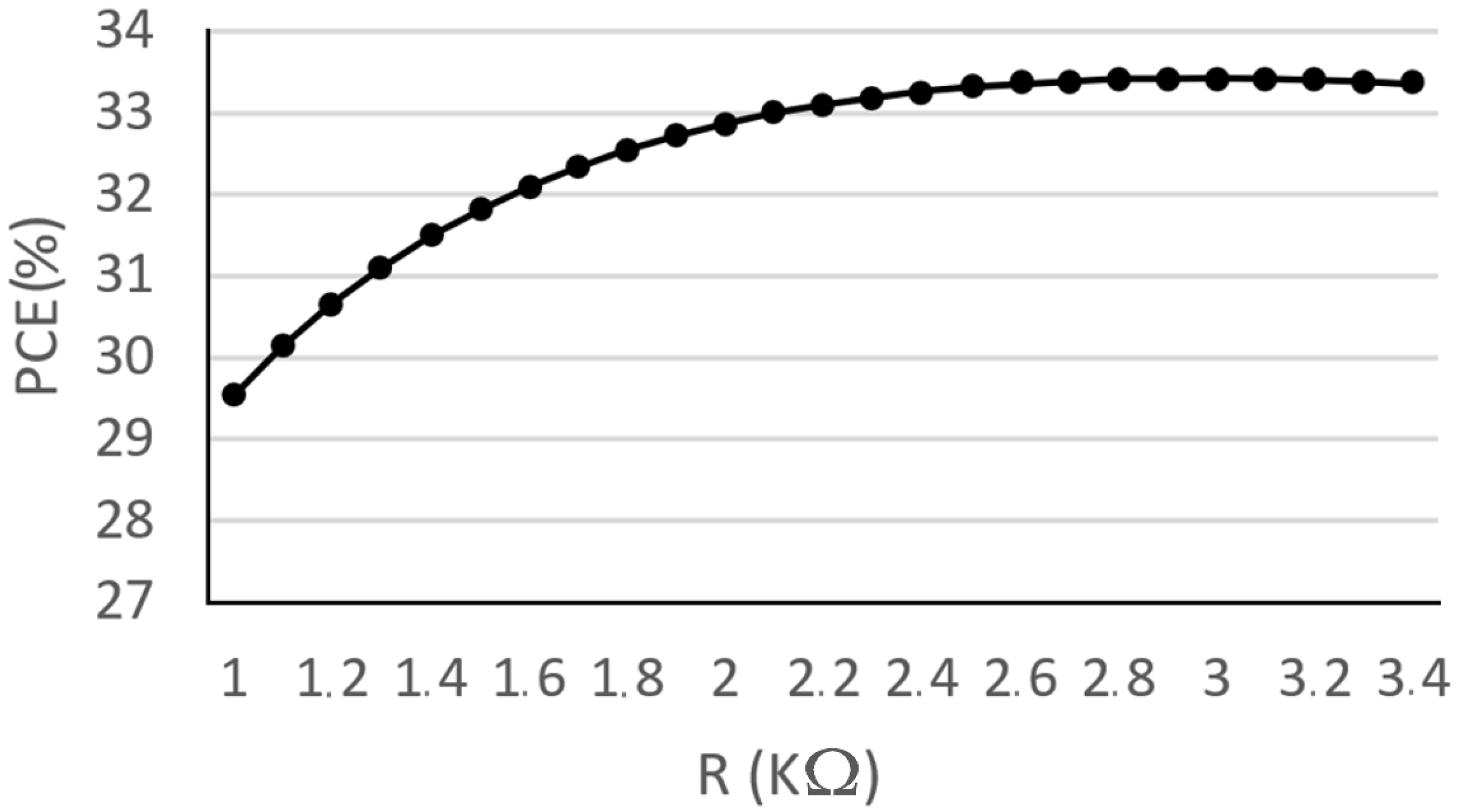
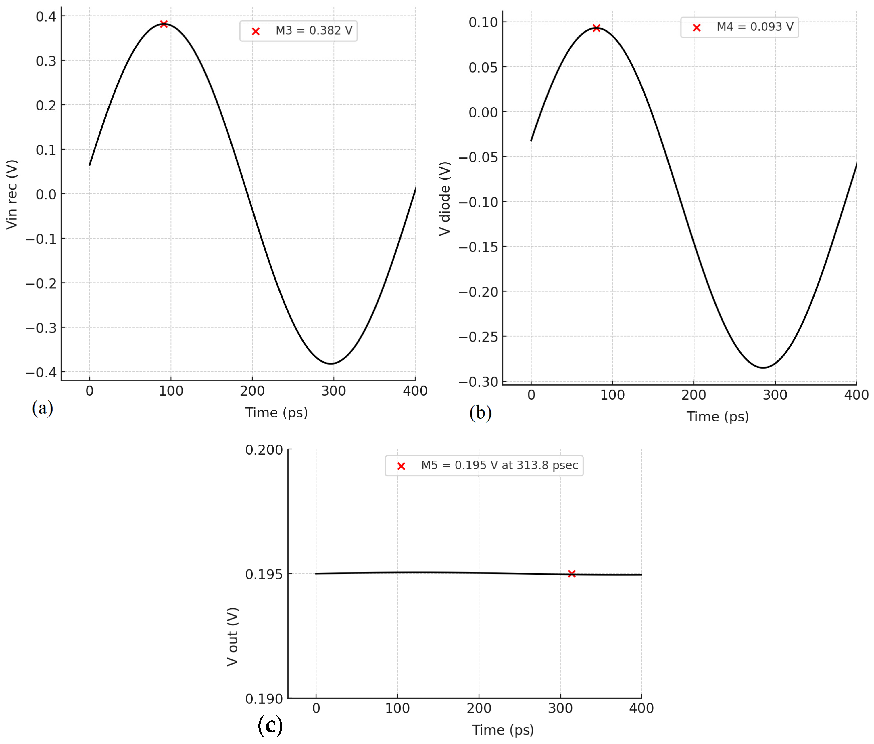
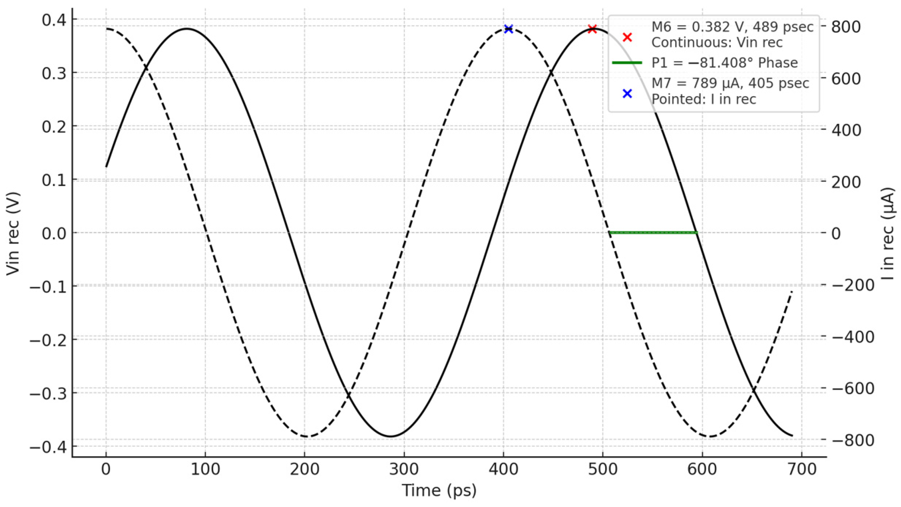
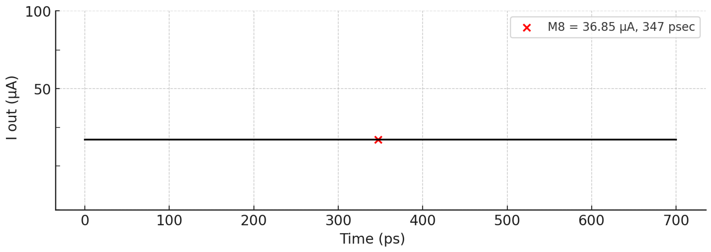
3.1.1. Diode Bridge Rectifier Baseline Simulation

A series of simulations aiming to maximize efficiency were conducted, and the results indicated an optimal load resistance of 3 KΩ when using the SMS7630 diode (Figure 8) and 2.9 KΩ when using the HSMS2850 diode [25], both with an input power of −15 dBm. Consequently, the load resistance should have a value of 3 KΩ or higher. To rectify and stabilize the voltage at the output, a capacitance of 100 pF was added; the results are presented in Table 3.

3.1.2. Impedance Matching with Discrete Component Selection for the Bridge Rectifier

Initially, impedance matching was achieved by using discrete components. For the HSMS2850 Schottky diode, the CL configuration showed better performance, while for SMS7630, the LC configuration (Figure 9) demonstrated better results (Table 4).

3.1.3. Impedance Matching Microstrip Selection for the Bridge Rectifier

When selecting a substrate, the following factors are considered: a dielectric constant (εr) of at least 3.5 for high frequencies such as 2.45 GHz, a low loss tangent (below 0.02) for better high-frequency performance, good thermal stability to maintain electrical characteristics, and board thickness (0.8–1.6 mm) adapted to the frequency and impedance needs.
After analyzing various substrates and considering the above-mentioned recommendations, we selected RO4350B [26].

3.1.4. Comparison of Impedance Matching Types

The data presented in Table 4 indicate that the SMS7630 diode displays superior power conversion efficiency (PCE) in comparison with the HSMS2850 diode. Furthermore, the discrete components employed in the impedance matching circuit revealed an S11 measurement of less than −30 dB, while the microstrip line configuration resulted in an S11 measurement of less than −40 dB [25].

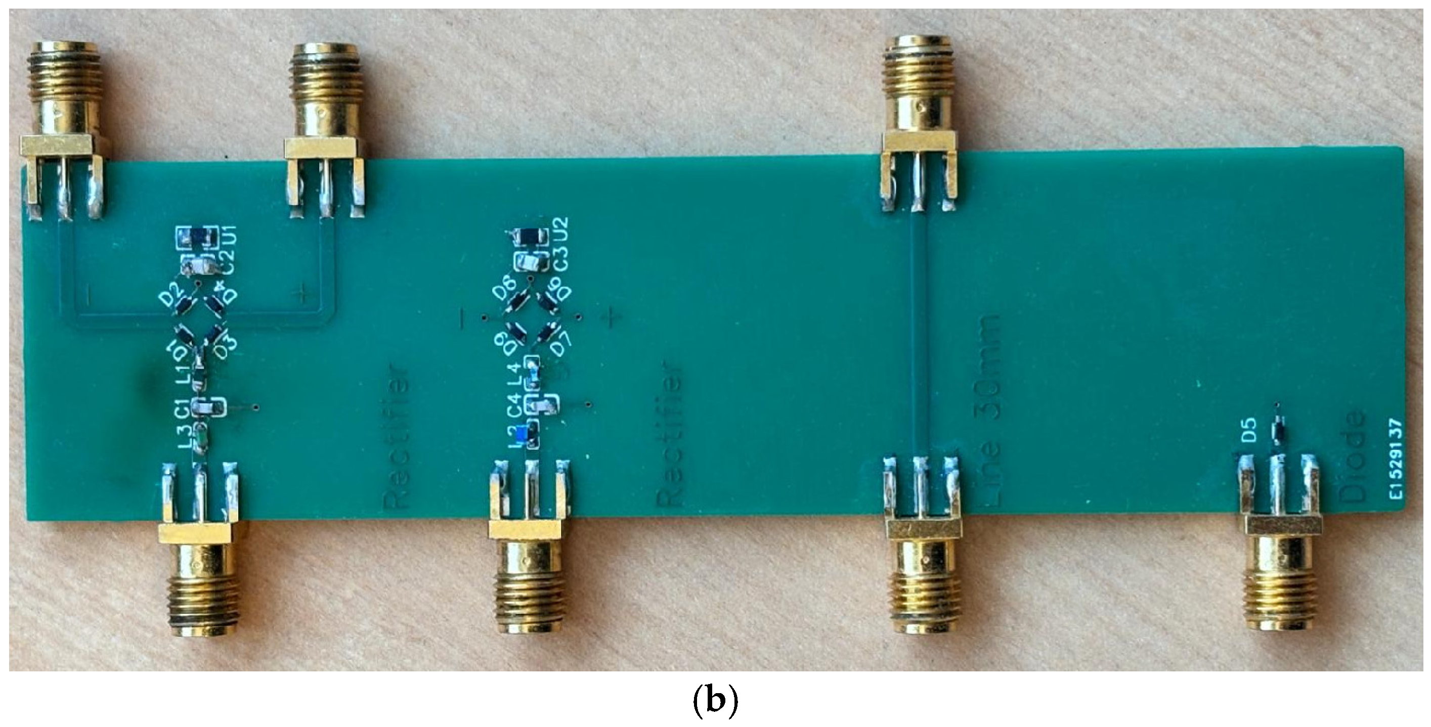
3.1.5. Bridge Rectifier Printed Circuit Board Realization

To validate the design through lab measurements, the rectifier must be implemented on a PCB. Microstrip lines, which are commonly used for interconnections in RF circuits, introduce challenges such as signal losses, phase shifts, and impedance mismatches. Therefore, it is important to include these characteristics in simulations in order to achieve results that reflect real-world performance. By using ADS and Momentum simulation software (Version 2021a), the following steps were taken for our final layout:
  • Addressing matching issues: After adding the microstrip line dimensions and the SMA connectors, we had to fine-tune the input matching by adjusting the original LC impedance matching network, replacing it with an LCL structure to maintain the same level of impedance matching.
  • Layout visualization: The final circuit layout was designed using EasyEDA (Figure 10).
  • Component placement and microstrip inclusion: The layout included a full diode bridge with SMA connector outputs. A second diode bridge without output SMA connectors was used in case the SMA connectors introduced parasitic effects during measurements. Additionally, a separate 30 mm transmission line segment was added to measure the linear losses associated with the microstrip lines if needed. Finally, a single diode was positioned at the bottom of the layout for individual characterization. The PCB dimensions were 3 cm × 23.6 cm and the rectifier dimensions were 3 cm × 0.7 cm.
The PCB layout has been received and lab measurements are planned, which will enable in the future a laboratory evaluation of the rectifier’s performance, which was previously limited to simulation.
It is important to note that, when ordering components to assemble the PCB, impedance matching elements and voltage regulator components (R load and capacitor) with the exact same values as those in the ADS simulation were not available on the market. By running several simulation iterations with market available components, we achieved a PCE of 31% (compared to 33%). The variation in the PCE as a function of the R load became relatively stable with a very minor variation above 3 KΩ, and a PCE value of 31% was achieved with an R load value of 5.3 KΩ. This experience highlights the practical challenges encountered in bridging the gap between theoretical design and physical implementation.

3.1.6. Theoretical Calculation

To better understand circuit behavior and power conversion, a detailed theoretical calculation was carried out on the SMS7630 diode bridge rectifier circuit shown in Figure 11.
The power conversion efficiency formula, the rectifier PCE, using the standard definition, is expressed as
P C E = P o u t P i n   r e c
where  P o u t  is the power delivered to the load, and  P i n   r e c  is the input power to the bridge rectifier circuit.
The output power  P o u t  can be expressed as
P o u t = V o u t I o u t
where:
  • V i n   r e c  is the peak input voltage;
  • V D i o d e  is the diode peak voltage;
  • I o u t  is the output current at load R.
By substituting  V o u t = V i n   r e c 2 V D i o d e ,  as in Figure 12, we obtain
P o u t = V i n   r e c 2 V D i o d e I o u t
The input power  P i n   r e c  for the rectifier circuit is expressed as
P i n   r e c = V i n   r e c   r m s I i n   r e c   r m s c o s ϕ
where
  • V i n   r e c   r m s  is the RMS value of the input voltage,  V i n   r e c   r m s = V i n   r e c 2 ;
  • I i n   r e c   r m s  is the RMS value of the input current,  I i n   r e c   r m s = I i n   r e c 2 ;
  • c o s ϕ  is the power factor, accounting for the phase shift  ϕ  between the voltage and current.
Therefore, the bridge rectifier PCE can be further expanded as
P C E = V i n   r e c 2 V D i o d e I o u t V i n   r e c 2 I i n   r e c 2 c o s ϕ
To verify our theoretical model, we conducted a series of ADS simulations with an input power of  P i n   r e c   = −15 dBm and R = 5.3 KΩ.
The  V i n   r e c V D i o d e , and  V o u t  values can be observed in Figure 13, confirming that the output voltage of  V o u t   = 0.195 V aligns with the theoretical formula:
V i n   r e c = 0.382   V   a n d   V D i o d e = 0.093   V .
V o u t = V i n   r e c 2 V D i o d e = 0.382 2 0.093 = 0.196   V .
The PCE was also validated with the simulation output values from ADS (Figure 14 and Figure 15), calculated as follows:
The following is given:
V i n   r e c = 0.382   V ,   V D i o d e = 0.093   V ,   I o u t = 36.85   µ A ,   I i n   r e c = 789   µ A ,
ϕ = 81,408 ° .
The efficiency calculation is based on Equation (8):
P C E = 382 2 93 36.85 382 2 789 2 c o s 81,408 °
P C E = 7.22 23.39 = 0.3061 = 30.61 %
The calculated bridge PCE aligns with the PCE observed in the ADS simulation (Figure 16), with only a minor deviation (31.8% vs. 30.6%).
By achieving this alignment, we provide a validated simple breakdown of the signal processing and the performance of the bridge rectifier.
To investigate the performance of an alternative topology for low input power applications, the next section explores a voltage doubler topology.

3.2. Schottky Diode Voltage Doubler Rectifier Results

The results demonstrated a PCE better than that of the diode bridge rectifier across the tested input power range by using the SMS7630 diode at an R load of 5.3 KΩ. The reduced component count and the diodes’ lower voltage drop contribute to its superior efficiency. At an input power of −15 dBm and −5 dBm, the Delon circuit achieved a PCE of 41.5% and 66.3%, respectively.
It is important to mention that topology selection depends on several factors related to the targeted application. A bridge rectifier offers higher output currents and better voltage regulation, making it suitable for applications where minimizing parasitic ripples in the output and achieving higher currents are critical. However, a voltage doubler provides a better PCE and doubles the output voltage, which is particularly advantageous for systems requiring a specific voltage level.

3.3. CMOS Technology Bridge Rectifier Results

In this section, we explore the performance and efficiency of CMOS technology in bridge rectifier configurations, highlighting the significance of transistor characteristics and operational modes.

3.3.1. Transistor Characterization

The selected NMOS transistor results showed a relatively low-threshold voltage (Vth), enabling current to start flowing at 200 mV. The results also showed that increasing the gate width (W) led to an increase in current flow (W = 100 µm and Vgs = 0.5 V, Vds = 0.5 V, Ids = 9 mA) [27].

3.3.2. Half-Wave Rectifier Analysis

In this section, the NMOS transistor was tested in a half-wave rectifier circuit in both diode and switch modes.
Compared with diode mode, configuring the transistor in switch mode resulted in lower power consumption.
To gain deeper insight into the transistor power consumption, its equivalent resistance was calculated in both modes, and the results demonstrated a lower equivalent resistance in switch mode than in diode mode, thus explaining the reduced power consumption and enhanced PCE.
These results underscore the benefits of using switch mode for half-wave rectifier applications in low-power applications [27].

3.3.3. Full-Wave Bridge Rectifier Analysis

To further continue the analysis, a full-wave bridge rectifier was simulated. Three distinct topologies were examined:
  • Four NMOS transistors, all configured in diode mode (Figure 17a).
  • Four NMOS transistors, with two operating in diode mode and two operating in switch mode (Figure 17b).
  • A combination of two NMOS and two PMOS transistors, all configured in switch mode (Figure 17c).
The performance of each topology was evaluated by adjusting four key parameters during the simulations to maximize output power and efficiency: the input power (Pin), transistor gate width (W), voltage holding capacity (C), and load resistance (R).
Table 5 presents the optimal settings for each topology, along with the resulting output power and efficiency. Topology 3 yielded the highest performance, achieving an efficiency of 69% at an input power of −5 dBm and 43.6% at an input power of −26 dBm [27].
The results show that Topology 3, utilizing NMOS and PMOS transistors in switch mode, achieved the highest efficiency and the lowest power consumption at low-input power levels [27].

3.4. Comparison of the Different Simulated Circuits and Their Results with the Existing Literature

Table 6 compares the PCEs of the proposed CMOS third topology bridge rectifier, the discrete-component SMS7630 diode bridge rectifier, and the voltage doubler with those in recent studies; the referenced results were provided earlier.
Our results demonstrate significantly higher PCEs at −5, −15, and −26 dBm input power levels, highlighting the effectiveness of the SMS7630 Schottky diodes and CMOS technology with the selected topology.
Finally, Table 7 details the advantages and disadvantages of each of the analyzed technologies and topologies.

4. Conclusions

In this paper, we explored various rectifier topologies and technologies for efficient RF energy harvesting at 2.45 GHz. Their performance in terms of PCE for low-power applications was compared with that of recently published works, demonstrating the possibility of providing a relatively high PCE by using easy-to-manufacture and low-cost topologies. Although the bridge rectifier demonstrated solid performance, the voltage doubler showed improved efficiency due to its reduced component count.
In parallel, CMOS-based rectifier topologies were analyzed to evaluate their potential for integration in compact, high-efficiency energy harvesting systems. The results show that CMOS rectifiers using a hybrid NMOS/PMOS configuration in switch mode can achieve a higher PCE than Schottky diodes, reaching up to 69% at −5 dBm and maintaining an efficiency of 43% at a low-power input of −26 dBm.
Furthermore, future research should explore methods for enabling these rectifier topologies to operate across broader or multiple frequency bands, thereby enhancing their capacity to harvest energy from diverse radio frequency sources. In addition, a careful examination of real antenna impedance matching at the input stage is essential to ensure optimal power transfer in real world applications.
Also, as a preparatory step towards establishing a standardized metric for evaluating these systems, this article proposed a structured multi-step approach to develop an FOM relying on a data science approach, including data collection, an exploratory data analysis, and a PCA. The proposed FOM not only captures significant performance metrics but also facilitates objective comparisons between rectenna systems.

Author Contributions

Conceptualization, G.K. and F.H.; methodology, G.K. and A.G.; validation, F.H. and S.S.; writing—original draft preparation, G.K.; writing—review and editing, G.K., A.G., F.H. and S.S.; supervision, S.S. and W.R. All authors have read and agreed to the published version of the manuscript.

Funding

This research received no funding.

Data Availability Statement

This article contains the results of the papers titled “Low power CMOS bridge Rectenna”, which was presented at the IEEE Conference on Antenna Measurements and Applications (CAMA), Guangzhou, China, 2022, and “2.45 GHz Low-Power Diode Bridge Rectifier Design”, which was presented at the International Conference on Microelectronics (ICM), Abu Dhabi, United Arab Emirates, 2023.

Conflicts of Interest

All authors declare that the research was conducted in the absence of any commercial or financial relationships that could be construed as a potential conflict of interest.

References

  1. Sze, S.M. Semiconductor Devices; Pioneering Papers; World Scientific: Singapore; Teaneck, NJ, USA, 1991; pp. 377–380. [Google Scholar]
  2. Fleming, J.A. Instrument for Converting Alternating Electric Current into Continuous Currents. Patent No. 803,684, 7 November 1905. [Google Scholar]
  3. Pearson, G.L.; Brattain, W.H. History of semiconductor research. Proc. IRE 1955, 43, 1794–1806. [Google Scholar] [CrossRef]
  4. Sze, S.M. Physics of Semiconductor Devices, 2nd ed.; Wiley: New York, NY, USA, 1981. [Google Scholar]
  5. Bougas, I.D.; Papadopoulou, M.S.; Psannis, K.; Sarigiannidis, P.; Goudos, S.K. State-of-the-Art Technologies in RF Energy Harvesting Circuits—A Review. In Proceedings of the 2020 3rd World Symposium on Communication Engineering, Thessaloniki, Greece, 9–11 October 2020. [Google Scholar] [CrossRef]
  6. Wang, C.; Yang, B.; Shinohara, N. Study and Design of a 2.45-GHz Rectifier Achieving 91% Efficiency at 5-W Input Power. IEEE Microw. Wirel. Compon. Lett. 2021, 31, 76–79. [Google Scholar] [CrossRef]
  7. Rotenberg, S.A.; Podilchak, S.K.; Re, P.D.H.; Mateo-Segura, C.; Goussetis, G.; Lee, J. Efficient Rectifier for Wireless Power Transmission Systems. IEEE Trans. Microw. Theory Tech. 2020, 68, 1921–1932. [Google Scholar] [CrossRef]
  8. Bouchair, D.; Boukerroum, F. Performance Analysis of Various Rectifier Topologies for 2.45 GHz RF Energy Harvesting Applications. In Proceedings of the 2023 International Conference on Advances in Electronics, Control and Communication Systems (ICAECCS), Blida, Algeria, 6–7 March 2023; pp. 1–6. [Google Scholar] [CrossRef]
  9. Halimi, M.A.; Surender, D.; Khan, T. Design of a 2.45 GHz operated Rectifier with 81.5% PCE at 13 dBm Input Power for RFEH/WPT Applications. In Proceedings of the IEEE Indian Conference on Antennas and Propagation, Jaipur, India, 13–16 December 2021. [Google Scholar] [CrossRef]
  10. Khan, D.; Bassim, M.; Shehzad, K.; Ain, Q.U.; Verna, D.; Asif, M.; Oh, S.J.; Pun, Y.G.; Yoo, S.; Hwang, K.C.; et al. A 2.45 GHZ high efficiency CMOS RF energy harvester with adaptive path control. Electronics 2020, 9, 1107. [Google Scholar] [CrossRef]
  11. Ghaleb, A.A.A.; Adam, I.; Yasin, M.N.M.; Zambak, M.F.; Yunus, R.N.A.R. A Dualband RF Rectifier for ISM and 5G Applications. In Proceedings of the 2024 IEEE 1st International Conference on Communication Engineering and Emerging Technologies (ICoCET), Kepala Batas, Penang, Malaysia, 2–3 September 2024; pp. 1–4. [Google Scholar] [CrossRef]
  12. Sedeek, A.; Tammam, E.; Hasaneen, E.-S. Design of an efficient 2.45 GHz RF rectifier for energy harvesting from low RF power density environment. In Proceedings of the 2020 International Conference on Innovative Trends in Communication and Computer Engineering (ITCE), Aswan, Egypt, 8–9 February 2020; pp. 268–271. [Google Scholar] [CrossRef]
  13. Khan, D.; Oh, S.J.; Shehzad, K.; Verma, D.; Khan, Z.H.N.; Pu, Y.G. A CMOS RF Energy Harvester with 47% Peak Efficiency Using Internal Threshold Voltage Compensation. IEEE Microw. Wirel. Compon. Lett. 2019, 29, 415–417. [Google Scholar] [CrossRef]
  14. Pandey, A.; Srivastava, A.; Pandey, A.; Sharma, A.; Kumar, R. Highly Efficient 2.45 GHz Rectifier Circuit for RF Energy Harvesting Applications. In Proceedings of the 2023 5th International Conference on Smart Systems and Inventive Technology (ICSSIT), Tirunelveli, India, 23–25 January 2023; pp. 200–203. [Google Scholar] [CrossRef]
  15. Sung, G.-M.; Chou, H.-Y.; Chen, Z.-W. Radio Frequency Energy Harvesting IC for ISM-915 MHz and 2.45 GHz Wireless Transmitter. In Proceedings of the 2021 IEEE International Future Energy Electronics Conference (IFEEC), Taipei, Taiwan, 16–19 November 2021; pp. 1–5. [Google Scholar] [CrossRef]
  16. Xu, P.; Flandre, D.; Bol, D. Analysis, Modeling, and Design of a 2.45-GHz RF Energy Harvester for SWIPT IoT Smart Sensors. IEEE J. Solid State Circuits 2019, 54, 2717–2729. [Google Scholar] [CrossRef]
  17. Coskuner, E.; Garcia-Garcia, J.J. Metamaterial impedance matching network for ambient rf-energy harvesting operating at 2.4 GHz and 5 GHz. Electronics 2021, 10, 1196. [Google Scholar] [CrossRef]
  18. Vital, D.; Bhardwaj, S.; Volakis, J.L. Textile-Based Large Area RF-Power Harvesting System for Wearable Applications. IEEE Trans. Antennas Propag. 2020, 68, 2323–2331. [Google Scholar] [CrossRef]
  19. Sidibe, A.; Takacs, A.; Dragomirescu, D.; Charlot, S. Flexible Printed Rectenna Based on a 2.45 GHz CPW Rectifier for Energy Harvesting Applications. In Proceedings of the 2023 53rd European Microwave Conference (EuMC), Berlin, Germany, 19–21 September 2023; pp. 677–680. [Google Scholar] [CrossRef]
  20. Lau, W.W.Y.; Siek, L. 2.45GHz wide input range CMOS rectifier for RF energy harvesting. In Proceedings of the 2017 IEEE Wireless Power Transfer Conference (WPTC), Taipei, Taiwan, 10–12 May 2017; pp. 1–4. [Google Scholar] [CrossRef]
  21. AVAGO Technologies. HSMS-285x Series Surface Mount Zero Bias Schottky Detector Diodes; Datasheet; AVAGO Technologies: Singapore, 2009; p. 3. [Google Scholar]
  22. SKYWORKS. Surface-Mount Mixer and Detector Schottky Diodes Datasheet; Datasheet; SKYWORKS: Sydney, Australia, 2021; p. 4. [Google Scholar]
  23. Song, F.; Guo, Z.; Mei, D. Feature Selection Using Principal Component Analysis. In Proceedings of the 2010 International Conference on System Science, Engineering Design and Manufacturing Informatization, Yichang, China, 12–14 November 2010. [Google Scholar] [CrossRef]
  24. Vaswani, N.; Chi, Y.; Bouwmas, T. Rethinking PCA for Modern Data Sets: Theory, Algorithms, and Applications. Proc. IEEE 2018, 106, 1274–1276. [Google Scholar] [CrossRef]
  25. Koubar, G.; Haddad, F.; Nessakh, B.; Sadek, S.; Rahajandraibe, W. 2.45GHz Low-Power Diode Bridge Rectifier Design. In Proceedings of the 2023 International Conference on Microelectronics (ICM), Abu Dhabi, United Arabe Emirates, 17–20 December 2023. [Google Scholar] [CrossRef]
  26. ROGERS Corporation. RO4000® Series High Frequency Circuit Materials; Datasheet; ROGERS Corporation: Chandler, AZ, USA, 2022; p. 3. [Google Scholar]
  27. Koubar, G.; Haddad, F.; Sadek, S.; Rahajandraibe, W. Low power CMOS bridge Rectenna. In Proceedings of the 2022 IEEE Conference on Antenna Measurements and Applications (CAMA), Guangzhou, China, 14–17 December 2022. [Google Scholar] [CrossRef]
Figure 1. Schematic of a rectenna system.
Electronics 14 00716 g001
Figure 2. Bridge rectifier baseline topology.
Electronics 14 00716 g002
Figure 3. Schottky diode voltage double rectifier topology.
Electronics 14 00716 g003
Figure 4. Eigenvalues of the principal components.
Electronics 14 00716 g004
Figure 5. Eigenvector decomposition.
Electronics 14 00716 g005
Figure 6. Synthetic example of the contribution diagram of M1,…M8 to the PCs.
Electronics 14 00716 g006
Figure 7. Synthetic example of PCA biplots: a figure of merit (FOM) with two principal components.
Electronics 14 00716 g007
Figure 8. Power conversion efficiency (PCE) as a function of the load resistance (R) using SMS7630 at −15 dBm.
Electronics 14 00716 g008
Figure 9. Rectifier system using LC for the impedance matching of SMS7630 bridge diodes.
Electronics 14 00716 g009
Figure 10. Bridge rectifier drawing (a) and realized printed circuit board for laboratory measurements (b).
Electronics 14 00716 g010aElectronics 14 00716 g010b
Figure 11. Full-wave bridge rectifier system.
Electronics 14 00716 g011
Figure 12. The equivalent circuit of the bridge rectifier during a rectification cycle.
Electronics 14 00716 g012
Figure 13. Bridge rectifier input (a), diode (b), and output (c) voltage for Pin = −15 dbm.
Electronics 14 00716 g013
Figure 14. Current and voltage signal and phase delta at the input of the bridge rectifier.
Electronics 14 00716 g014
Figure 15. Current signal at the output of the bridge rectifier.
Electronics 14 00716 g015
Figure 16. ADS simulation results of the bridge rectifier efficiency Pout/Pin.
Electronics 14 00716 g016
Figure 17. Configurations of full-wave bridge rectifier topologies: (a) Topology 1, (b) Topology 2, and (c) Topology 3.
Electronics 14 00716 g017aElectronics 14 00716 g017b
Table 1. List of criteria.
Group A: Power conversion efficiencyM1: Antenna gain
M2: Matching network efficiency (Pin/Pavailable)
M3: Power conversion efficiency (Pout/Pin)
M4: Power factor (Pout/Pavailable)
M5: Start-up power (Pin)
Group B: Voltage performanceM6: Output voltage (Vout)
M7: Start-up voltage (Vin)
Group C: Current dynamics and energy storageM8: Forward vs. reverse current time ratio
M9: Isolation between AC input and DC output
Group D: Signal qualityM10: Harmonic distortion levels
M11: Ripple factor in DC output
Group E: Operational stability and reliabilityM12: Operating bandwidth
M13: Thermal stability
Table 2. Dataset matrix of circuits and criteria.
Dataset MatrixM1(…)M13
Circuit 1(…)(…)(…)
(…)(…)(…)(…)
Circuit N(…)(…)(…)
Table 3. Power conversion efficiencies (PCEs) of the baseline topology.
Input Power (dBm)PCE (%)
HSMS2850−553
SMS7630−560
HSMS2850−1524
SMS7630−1533.5
Table 4. Overall summary of the PCEs for the different impedance matching options.
Input Power (dBm)PCE (RO4350B Line) (%)PCE (Discrete Components) (%)
HSMS2850−54049
SMS7630−55257
HSMS2850−151623
SMS7630−152933
Table 5. Output power and efficiency results by topology.
Frequency = 2.45 GHzTopology 1Topology 2Topology 3
Input power = −5 dBmW = 110 µm, C = 10 pF, R = 650 Ω
PCE (%)284069
Input power = −26 dBmW = 110 µm, C = 19.95 fF, R = 12.5 KΩ
PCE (%)1317.843.6
Table 6. Comparison of the power conversion efficiency (PCE) in this work with those in other recent works.
ReferenceInput Power (Pin) (dBm)PCE (%)
[6]3791
[7]2775
[8]1577
[9]1381
[10]645
[11]570
[12]3.574
[13]147
[14]0.852
[15]030
[16]−348
[17]−541
This work (diode bridge rectifier)−557
This work (diode voltage doubler)−566
This work (CMOS bridge rectifier)−569
[10]−620
[18]−1035
[19]−1037
[20]−1259
This work (SMS7630 diode bridge rectifier)−1533
This work (diode voltage doubler)−1541.5
[17]−1527
This work (CMOS bridge rectifier)−2643
Table 7. Advantages and disadvantages of the three topologies using the Schottky diodes and CMOS transistors.
CircuitAdvantagesDisadvantagesPCE
Diodes: full-wave bridge rectifierHigh output current and controller ripplesHigh consumption due to the higher number of diodes (four)+
Diodes: voltage doublerHigh voltage outputRisk of ripples on the output++
CMOS: full-wave bridge rectifierCompact designHigh cost+++
Plus signs compare different topologies to each other.
Disclaimer/Publisher’s Note: The statements, opinions and data contained in all publications are solely those of the individual author(s) and contributor(s) and not of MDPI and/or the editor(s). MDPI and/or the editor(s) disclaim responsibility for any injury to people or property resulting from any ideas, methods, instructions or products referred to in the content.

