Abstract
As application conditions become increasingly demanding and usage becomes more aggressive, the performance of traditional insulated gate bipolar transistor (IGBT) and fast recovery diode (FRD) systems can no longer meet the required specifications. In these systems, FRDs are required to carry load current and allow current to return from the load to the IGBTs. Consequently, the reverse recovery performance of the FRDs significantly restricts the overall efficiency of the system. Therefore, how to predict the reverse recovery characteristics of the FRDs with greater precision has attracted considerable attention. In this context, this paper presents an in-depth investigation of the high-level injection carrier distribution and reverse recovery characteristics of punchthrough P-I-N (PT-PIN) FRD with a buffer layer. Specifically, the research explores the physical properties of the materials, doping concentrations, and the geometric structure of the devices. Furthermore, it takes into account the complex interactions among carrier recombination, diffusion, and drift, leading to the development of a model that delineates the spatial distribution of carriers and their influence on current conduction. Building upon the traditional step-wise analysis method, subsequently, the temporal aspects of the FRDs reverse recovery process were further segmented. Utilizing the derived carrier distribution model, a reverse recovery analytical model was constructed. The model was validated using a 1200 V, 100 A IGBT with 1200 V, 60 A FRD configured in a reverse parallel arrangement, which demonstrated a 5% improvement in prediction accuracy of VR compared with previous models that employed the lumped charge method. Finally, a range of experiments with varying RG, VCC and IF confirmed the broad applicability of this analytical model.
1. Introduction
In recent years, in power electronic circuits, IGBTs and FRDs are commonly used in conjunction with inductive loads to conduct double pulse tests. During the turn-on process of the IGBT, it is necessary for the FRD to carry the load current and allow the current to return from the load to the IGBT, which involves the reverse recovery characteristics of the FRD [1,2]. During this phase, the transition of voltage applied to the anode of FRD from a positive to a negative state results in a gradual decline of the current traversing the diode, which decreases at a steady rate. The reduction in current persists until all charges within N− drift are completely discharged, resulting in the establishment of a depletion region that enables the PN junction to endure the associated reverse voltage. The stored charge leads to a notable peak in reverse recovery current (IRR), which subsequently decreases gradually to zero. This phenomenon characterizes the reverse recovery process of the FRD.
In the field of semiconductor technology, the modeling methods for PIN diodes are contingent upon their applications and the specific requirements of their characteristics. These methods can primarily be categorized into four types: behavioral models, numerical models, physical models, and hybrid models [3,4,5]. The transient behavior of PN junction diodes has been proposed to be accurately predicted using a simple piecewise linear model, which consists of a linear resistor and a linear capacitor. The precision of this model has been validated through both simulations and experimental findings, with a notable strength in its capability to analyze intricate and chaotic nonlinear behaviors in series resonant converters, as well as in various real-world electronic circuits [5]. Nevertheless, its limitations are also evident; behavioral models typically focus on the macroscopic performance of devices. Although they exhibit faster algorithm speeds in specific applications, they fail to provide in-depth analysis and capture the internal carrier characteristics of the devices. Subsequently, a charge-controlled numerical model for PIN-FRDs was proposed, taking into account the additional contact layer that stores charge. This portion of stored charge significantly influences the forward steady state and the turn-off transients (switching time and conversion loss) [6]. The numerical model demonstrates exceptional accuracy, capable of simulating the current–voltage characteristics of devices and their responses to temperature variations through numerical methods. However, obtaining critical structural parameters from manufacturers is necessary to ensure the model’s accuracy and effectiveness [7].
In contrast, physical models are grounded in the principles of quantum mechanics and solid-state physics, revealing the behavioral patterns of charge carriers within semiconductor materials. Such models are capable of accurately describing the operational characteristics of PIN diodes across various operating states, encompassing a broad range of attributes from static to dynamic and from steady-state to transient conditions while also capturing variations in the internal charge distribution of the devices [8,9,10,11]. A SPICE circuit model for diodes has been introduced, incorporating factors such as recombination at the emitter in the heavily doped terminal region, conductivity modulation within the base region, and the effects of moving boundaries throughout the reverse recovery phase. The results indicate that both quasi-static models and lumped charge models can be approximated using low-order matrix matching, while higher-order solutions yield new, more accurate models characterized by good convergence and rapid simulation times [8]. Subsequently, the physical model for high-voltage fast recovery diodes was refined. This model achieves an optimal balance between reverse recovery time and forward voltage drop by integrating techniques for lifetime management and reductions in emitter efficiency. Additionally, research has shown that reducing the number of excess charge carriers stored in N− drift results in softer characteristics, which can be achieved with lower doping levels [9]. In recent years, a refined thermal–electrical model for power diodes has been introduced, grounded in the numerical solution of the bipolar diffusion equation (ADE), which considers significant localized physical phenomena. This model effectively monitors both electrical and thermal effects, including the self-heating of the device during its operational phase [10]. Subsequently, the lumped charge method for buffered diodes was adjusted to investigate the impact of the buffer layer as well as techniques for controlling carrier lifetime. The relationship between carrier lifetime and the injected charge was examined, resulting in the formulation of a lumped charge model specifically for carrier lifetime. This model integrates supplementary temperature functions for the physical parameters to derive both its static and transient thermal characteristics, which were subsequently implemented within the circuit simulation platform PSPICE [11].
The hybrid model integrates the advantages of the aforementioned various models, enhancing the overall performance through appropriate synergistic interactions and data fitting. This approach provides a more flexible solution for the modeling and simulation of complex circuits. The issues of short reverse recovery in PIN diodes within typical power conversion circuits were investigated under different initial current conditions. By establishing boundary connections during the transition phases of conduction and cutoff, a hybrid model for the peak reverse recovery voltage of diodes under short-duration conditions was ultimately developed. This model combines physical and behavioral aspects with model parameters extracted through measurement and circuit extraction methods, thereby reducing complexity [12]. However, it is noteworthy that most current research still relies on traditional PIN-FRD models, with relatively little focus on FRD devices featuring a punchthrough buffer layer. Although the lumped charge method has predicted reverse recovery characteristics with considerable accuracy, the current research approaches exhibit ambiguity regarding the temporal delineation, and the interactions of carrier recombination, diffusion, and drift within the lumped charge method remain inadequately articulated. The large-injection distribution model and reverse recovery analytical model proposed in this study accurately characterize the reverse recovery behavior of punchthrough P-I-N (PT-PIN) FRD with a buffer layer.
The rest of this paper is organized as follows: Section 2 will present a comprehensive derivation of the carrier distribution in fast recovery diodes (FRDs) under conditions of significant injection. Section 3 will derive the reverse recovery process through a stepping analysis method based on the established carrier distribution. Section 4 will describe the experimental testing platform that was constructed, as well as the physical parameters of the devices. Section 5 will conduct a comparative validation of traditional models, analytical models, and experimental results, as well as assess the applicability of the analytical model under varying testing resistance conditions. Finally, Section 5 concludes the paper.
2. Analytical Model of Carrier Distribution in FRDs Under the High-Level Injection Conditions
Table 1 below elucidates the physical significance of the parameters employed in this study.

Table 1.
Physical meaning of the parameters.
2.1. Analytical Model of Carrier Distribution in the Conventional PIN-FRD Suspended Wire Structure
In the moment preceding reverse recovery, the FRD is in a conductive state under large injection conditions. To enable the subsequent derivation of the analytical model, it is crucial to first establish the carrier distribution within the FRD. Only with a lighter doping concentration in N− drift can FRD effectively endure high reverse bias voltage levels. During the process of forward conduction, the concentration of minority carriers increases with the rising voltage drop, in accordance with the “junction law” (Shockley boundary condition), as expressed by the following equation [13]:
Eventually, the intrinsic doping concentration in N− drift is characterized by a value lower than that of the minority carrier concentration, denoted as ND. This occurrence is termed heavy injection. Immediately prior to the turn-off of the FRD, the device operates under conditions of heavy injection, where the requirement for charge neutrality stipulates that the electron concentration n(x) matches the hole concentration p(x):
The distribution of carrier concentrations n(x) and p(x) within N− drift can be derived by solving the continuity equations [12]:
In the equations, D represents the diffusion coefficients, respectively, while τHL denotes the charge carrier’s lifetime. By multiplying Equations (3) and (4), the results can be combined to yield the following:
In deriving the aforementioned expression, it is assumed that the current generated by carrier diffusion can be considered negligible in comparison to the carriers extracted by the electric field. The relationship between the diffusion coefficient and mobility can be obtained through the Einstein relation:
According to the Formula (2), when the electron and hole carrier concentrations are equal, the steady-state condition allows the equation to be expressed as follows:
In the equation, Da represents the bipolar diffusion coefficient, which can be expressed in terms of the charge neutrality condition as follows:
The general solution for carrier concentration can be computed from the Equation (7):
In this context, the constants A and B are established based on the boundary conditions relevant to the N− drift. La can be expressed by the following formula:
The right boundary is delineated at the junction between N− drift and N+ cathode, where the current is conducted by electron transport:
Similarly, the left boundary is defined at the junction between N− drift and P+ anode, where the current is facilitated by hole transport:
Utilizing Equation (11), the hole current can be expressed as follows:
By combining the Equation (2) with the Einstein relation, the following expression can be obtained:
The equation describes the total current generated by electron transport at this boundary and can be expressed as
By utilizing the electric field E(+d) in the Equation (14), it can be concluded that
Similarly, it can be derived that
By applying the aforementioned boundary conditions (16) and (17), the constants A and B in the Equation (9) can be determined, resulting in the following:
Equation (18) describes the charge carrier concentration distribution of a catenary structure, as illustrated in Figure 1.
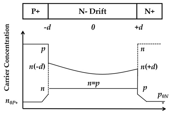
Figure 1.
Carrier distribution of the conventional PIN-FRD under high-level injection condition.
2.2. Analytical Model of Carrier Distribution in the Punchthrough P-I-N (PT-PIN) FRD with a Buffer Layer with a Suspended Wire Structure
Indeed, the presence of a buffer layer leads to alterations in the internal carrier distribution. The introduction of the buffer layer facilitates a stepwise transition from N− drift to N+ cathode. Carrier distribution within the buffer layer FRD can be represented using a piecewise function, with the thickness W that terminates at N− drift serving as the delineation point. The first segment is represented using a conventional PIN-FRD structure, while the subsequent segment, which spans from the buffer layer to the N+ cathode, continues to adhere to the general solution for carrier distribution, as described by the Equation (9). At this stage, it can be expressed as
In the equation, La2 denotes the bipolar diffusion length specific to the buffer layer. At the junction between the buffer layer and N+ cathode, the total current is wholly carried by electron transport, thus fulfilling the right boundary condition (16).
The left boundary condition is defined by the carrier concentration in N− drift at the position +W:
By substituting the Equation (19), the left boundary condition is obtained through the following solution:
By simultaneously applying the conditions (16) for the right boundary, the constants A2 and B2 in the Equation (19) can be derived, leading to the determination of the carrier distribution from the buffer layer to the N+ cathode.
Let
In fact, the carrier lifetime following electron irradiation is determined by Equation (25):
Consequently, due to the differing bipolar diffusion coefficients between N− drift and buffer layer, it follows that
Equation (26) expresses a carrier distribution model for the PT-PIN FRD with a buffer layer, as illustrated in Figure 2.
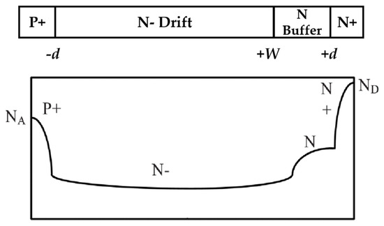
Figure 2.
Carrier distribution of the PT-PIN FRD with a buffer layer under high-level injection condition.
2.3. Establishment of an Analytical Model for the Reverse Recovery Characteristics of PT-PIN FRD with a Buffer Layer
The average carrier concentration introduced into N− drift declines as carrier lifetime shortens, a correlation that can be established through charge control theory. Under steady-state conditions, if recombination processes occurring within the terminal region are disregarded, the current passing through the FRD is linked to the ongoing recombination of electrons and holes within N− drift. Therefore
where R denotes the recombination rate, expressed by the following equation:
By utilizing the average carrier concentration in N− drift, denoted as na, Equations (27) and (28) can be simultaneously solved to yield the following:
It is assumed that the concentration of carriers within N− drift can be linearized. With a constant dIC/dt, an analytical model can be developed to analyze the characteristics of the FRD. This methodology was originally referred to as the stepwise recovery process. As depicted in Figure 3, the distribution of carrier concentrations established during the conducting state can be approximated by the linear variation between the average concentration n(−d) at the midpoint of the drift region x = 0 and the average carrier concentration na at x = b [14,15,16]:
where JF represents the forward current.
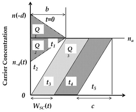
Figure 3.
Carrier distribution of PT-PIN FRD with a buffer layer during the reverse recovery process.
This study integrates the structure of the FRD with its reverse recovery waveform. A typical PT-PIN FRD with a buffer layer structure [17,18], along with a standard reverse recovery waveform, is presented below in Figure 4.
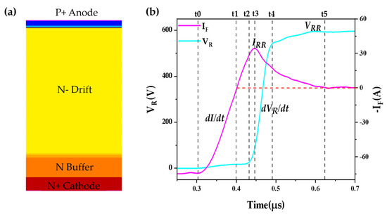
Figure 4.
(a) Structure of PT-PIN FRD with a buffer layer; (b) typical reverse recovery waveform.
During the early stage of reverse recovery, the current density of FRD shifts from the forward current JF to 0 at time t1. As illustrated in Figure 3, the distance b can be ascertained by concurrently solving for the charge Q1 that is extracted during the initial phase alongside the current. At the end of this phase, specifically at time t1, the carrier distribution becomes homogeneous owing to the lack of current. At this stage, the variation in charge can be represented by the region designated as Q1 in Figure 3.
This charge is related to current during reverse recovery from t = t0 = 0 to t = t1:
In the equation, a denotes a constant dIC/dt. The moment at which the current reaches zero, denoted as t1, can be expressed by the following equation:
By simultaneously solving Equations (30)–(33), the following result is obtained [17]:
where
The second phase begins when the current becomes 0 at t1 and continues until t2, when the p+/n junction begins to endure reverse bias voltage. Figure 3 depicts that at t2, the distribution of carrier concentration ranges from zero at the junction located at x = 0 to na at a distance b away from the junction. Subsequent to t2, the carrier concentration at a certain distance from the p+/n junction approaches zero, resulting in the formation of a depletion region at the p+/n junction. The moment t2 can be determined by analyzing the charge extracted from t = t1 to t = t2. The area marked as Q2 in Figure 3 describes the charge extracted during this interval. The area of this region is given by the following equation:
This charge is related to the current from t = t0 to t = t1:
By simultaneously solving Equations (36) and (37) and utilizing Formula (29) for na along with Formula (34) for the distance b, we obtained the following [18]:
In the third phase, the voltage across FRD begins to increase continuously. This increase requires the development of a space charge region (SCR) WSC(t) at the P+/N junction. Figure 3 illustrates the progressive extension of SCR over time, accomplished through the additional extraction of charge that is stored in N− drift, leading to a sustained rise in reverse current following the moment t2. Assuming that the current during the extraction of stored charge remains approximately constant, an analytical model can be employed to analyze the increase in reverse bias across the FRD terminals. After the time t2, the p+/n junction is subjected to reverse bias, and the variation in charge is illustrated by the region designated as Q3 in the figure. The area of this region is defined by the following equation:
This charge is associated with the current from t2 to t:
The relationship established in conjunction with Q3 indicates that the extension of the SCR is a function of time.
The voltage experienced by SCR can be derived from the solution of Poisson’s equation.
In this context, Q(x) denotes the charge within SCR. During reverse recovery, the significant reverse current supplies additional charge to the depletion region. Due to the significant electric field present, it can be assumed that these holes drift at a saturation velocity, denoted as (Vsat, p). The concentration of holes within SCR is linked to the current density JR through the following relationship:
Thus, the voltage across SCR is expressed by the following equation:
In conjunction with Equation (44) describing the extension of SCR, the aforementioned expression illustrates that the voltage across the FRD experiences a rapid increase after the time t2. It is important to note that the endpoint of the third phase varies for different FRD structures. For the conventional PIN-FRD, the third phase concludes when the reverse bias voltage across the FRD equals the applied supply voltage. However, in the case of the PT-PIN FRD with a buffer layer, which is the focus of this study, the third phase ends when the depletion region extends to the N− drift region, at which point the depletion region reaches the left boundary of the buffer layer. As shown in Figure 5, the electric field distribution when the depletion region contacts the buffer layer can be obtained by solving Poisson’s equation.
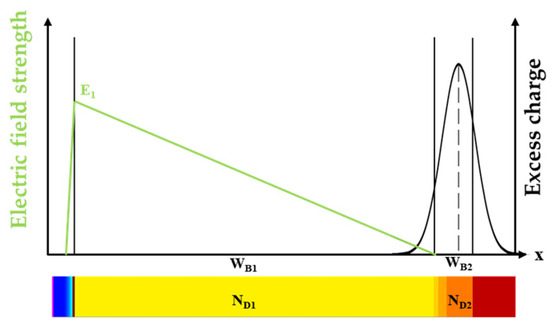
Figure 5.
Electric field intensity and excess carrier distribution when depletion layer extends to buffer layer.
At this point, the voltage across the device can be determined by integrating the area under the curve.
Since the concentration of free-moving charge carriers within the buffer layer is significantly lower than that in N− drift, the concentration of free-moving charge carriers in the buffer layer can be neglected. Consequently, when the depletion layer extends into the N− drift, the reverse bias voltage at this moment corresponds to IRR, allowing for the determination of t3, the time at which IRR is reached.
In the fourth stage, the current declines swiftly at nearly a constant rate. In Figure 3, the charge retained in N− drift at the end of the third phase is indicated as Q4. At the conclusion of this phase, specifically when t = t3, the IRR flows through the structure. This current can be related to the profile of free carriers in the following manner:
The dimension h can be obtained using the formula, where Da is determined by the parameters of the buffer layer, and na is calculated according to the specified Equation (26) x > +W.
Thus, the remaining stored charge in N− drift at the time t3 can be expressed as
During the fourth stage, the charge retained in N− drift must be entirely extracted and collected in the buffer layer, with t4 representing the duration required for this phase. Throughout this stage, the current decreases at a rate that remains approximately constant. The charge extracted and accumulated in the buffer layer during this interval, due to the extension of the depletion layer, can be expressed as
This can be likened to the charge that persists in N− drift at the end of the third stage. If the length of this interval is comparatively brief in relation to minority carrier lifetime, the effects of recombination may be disregarded. Consequently, this leads to the determination of the time t4 for the decrease in the reverse current:
The rate of reverse slope can be obtained by dividing IRR by the corresponding time:
In the fifth stage, the FRD enters the phase involving the buffer layer, characterized as a heavily doped N− drift, as shown in Figure 6. Doping concentration within this layer must be sufficiently elevated to avoid total depletion under the reverse bias applied across the FRD. Concurrently, the doping concentration of the buffer layer must remain sufficiently low to facilitate conductivity modulation, thereby preserving a certain quantity of stored charge within the layer. In the fifth stage, the applied bias fails to efficiently extract this stored charge, leading to a diminished rate of current.
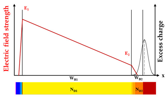
Figure 6.
Electric field intensity and excess carrier distribution of depletion layer spreading in buffer layer.
Unlike conventional PIN structures, when the depletion layer interfaces with the buffer layer, the substantial doping concentration of the buffer layer hinders the extension of the depletion region. Since the time required for the extension of the depletion layer is relatively long compared to the minority carrier lifetime, the stored charge within the buffer layer cannot be extracted through the extension of SCR. Instead, as shown in Figure 7, it dissipates via recombination [19,20]. Since SCR is subjected to voltage, it can be assumed that the electric field in the undepleted area is negligible when excess carriers diffuse. As a result, the drift component of the excess carrier current can be disregarded in the continuity equation.
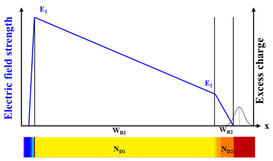
Figure 7.
Electric field intensity and excess carrier distribution of hole recombination in fifth stage.
Consequently, the concentration of excess carriers [δp(x,t)] in the fifth stage is governed by the following equation:
In Figure 3, it is illustrated that the concentration of excess carriers is 0 at the boundary of SCR during the fourth stage, while it attains its maximum at the center of the undepleted area. If we define the distance from the center of the undepleted region to the boundary of SCR as
The maximum concentration of excess carriers is located at:
The maximum concentration of excess carriers is expressed by the following equation:
Here, Δp can be calculated from the concentration of excess carriers at the position x = xM at the onset of the fifth stage. Assuming that the concentration of excess carriers at this location when the fifth stage begins (at t = t4) is equal to the average carrier concentration na, the following is obtained:
Utilizing the boundary conditions
This results in the distribution of free carrier concentration in the undepleted region.
Here, Δx represents the distance to the position x = xM, while the time t refers to any moment after t = t4, which marks the conclusion of the fourth stage. The current during the fifth stage can be calculated using the distribution of free carrier concentration:
Substituting into the above equation yields the current:
As discussed above, the entire reverse recovery process can be derived from the analytical model.
3. Device Physical Parameters and Experimental Setup
3.1. Physical Parameters of the Device
To validate the accuracy of the analytical model, the device under investigation is the ASD060T12S11T FRD product developed by Archimedes Semiconductor Co., Ltd. in Hefei, Anhui Province, China. This FRD device is housed within a TO-247-Plus-4L package, specifically the ADG100N12MTA model, functioning in a parallel configuration. The physical and structural parameters of the device are presented in Table 2. The carrier lifetime control technique utilized in this study for the FRD is facilitated through electron irradiation, with an irradiation energy of 10 MeV and a dosage of 120 kGy. An analysis of the defect distribution in the device using Deep Level Transient Spectroscopy (DLTS) was performed, as illustrated in Figure 8. A preliminary estimate of the carrier lifetime was obtained by referencing the findings presented in [21].
Table 2.
Physical structure and process parameters of PT-PIN FRD with a buffer layer.
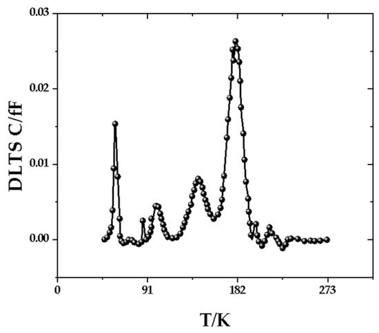
Figure 8.
FRD base region DLTS testing under a 120 kGy (Si) electron irradiation dose.
3.2. Construction of Experimental Platform
Figure 9a shows the structural diagram of TO-247Plus packaging of discrete devices after dicing the wafer. Figure 9b shows the internal composition of the discrete device, with a 1200 V 100 A IGBT parallel to a 1200 V 60 A FRD. Figure 9c shows the setup of the double pulse test platform for power devices; Figure 9d illustrates the principles of the double pulse test. The DC bus voltage Vcc is provided by a high-voltage DC power supply. The stray inductance of the test system Ls is 100 nH, RG(off) is set to 15 Ω, and RG(on) is set to 10 Ω. During the testing process, in order to ensure minimal stray inductance in the DC bus, T1 serves as the auxiliary bridge arm, whereas T2 is the device under test (DUT). A gate signal is applied to the auxiliary bridge arm to initiate its switching state. The following parameters need to be monitored during the test: diode voltage VR and diode current IF. The testing conditions are outlined in Table 3 below.
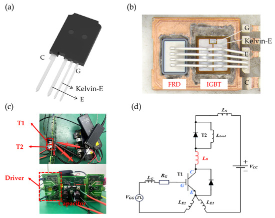
Figure 9.
(a) Structure diagram of discrete device TO-247Plus package; (b) internal chip diagram of discrete device TO-247Plus package; (c) power device double pulse characteristic test platform; (d) schematic diagram of double pulse test.
Table 3.
Experimental and circuit test conditions.
Figure 9c presents the setup of the double pulse test platform. Table 4 below provides information regarding the equipment utilized, including the oscilloscope, probes, and other devices.
Table 4.
Test equipment used model number.
4. Experimental Certification and Discussion
4.1. Analytical Model Verification
A comprehensive analysis was conducted on the results obtained from the analytical model curves in comparison with the measured curves in order to validate the model’s effectiveness and accuracy. During the research process, the current curve of the FRD was intentionally processed in reverse to facilitate observation and comparison, as illustrated in Figure 10. Overall, the analysis of the fitting results indicates a good correspondence between the analytical model and the measured curves, accurately predicting the reverse recovery characteristics of the FRD. However, in terms of detail, two primary sources of error were identified: one occurring during the early stage of current rise and the other during the initial phase of voltage rise.
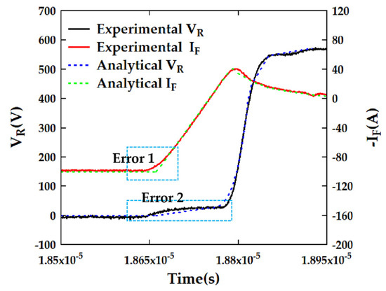
Figure 10.
Validation of the analytical model for reverse recovery of PT-PIN FRD with a buffer layer.
First, attention must be paid to the error observed during the initial rise of the current, referred to as Error 1. The current characteristics are governed by the IGBT, and the transconductance parameters of the IGBT influence the slope of the current rise. Due to the relatively low transconductance of the IGBT in the low current region, the measured waveform displays a slow slope during the early stage of current rise, resulting in a relatively gentle ascent curve. In contrast, the derived analytical model assumes that the FRD maintains a constant slope during reverse recovery; this assumption fails to accurately reflect the actual behavior of the FRD during the initial rise of current, thereby leading to this discrepancy.
Secondly, Error 2 during the initial rise of voltage is primarily manifested as a voltage step phenomenon in the measured waveform. During the testing process, a distinct step in voltage was observed during the rising phase of the measured waveform, which is primarily attributed to the parasitic inductance present in the switching circuit of the IGBT and FRD. The effect of parasitic inductance can induce transient variations in voltage, particularly during the switching instant when the rate of change in the current is significant; the back electromotive force generated by the inductance can lead to a temporary surge in voltage. The analytical model does not account for the presence and influence of parasitic inductance during this phase, resulting in deviations in the predicted voltage changes.
Error 2 in Figure 10 can indeed be attributed to the presence of parasitic elements. Postulate that this error arises from the stray inductance associated with the IGBT and FRD circulation loop rather than from the system’s stray inductance, LS. The stray inductance along the circulation path of the IGBT and FRD can be designated as LH. As illustrated in Figure 9d, the voltage elevation during the initial state based on the relevant equations can be derived. The model will incorporate the waveform resulting from stray inductance effects on the initial voltage state. As illustrated in Figure 11, the model’s accuracy in the early voltage phase has been enhanced by taking stray inductance into account.
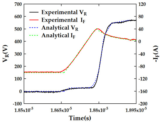
Figure 11.
Validation of the analytical model for reverse recovery by taking stray inductance into account.
As shown in Figure 10 of the manuscript, in addition to errors 1 and 2, discrepancies are also observed in the IRR position and the IF tailing during the final stage of reverse recovery. Overall, we attribute the errors to two primary sources: the first being testing errors, which encompass the influence of system components such as parasitic elements, and the second being FRD device-related errors, which stem from variations in physical parameters. Test errors will be further discussed in detail in Section 4.3.
Here, we aimed to provide a more detailed explanation of the FRD device-related errors. The FRD itself is subject to manufacturing process variations, and full consistency across different production batches cannot be guaranteed. As a result, variations in the FRD device’s physical parameters can occur, leading to discrepancies between the predicted model and the experimental curves. Errors in the IRR and IF tailing can be traced back to this factor. To further substantiate our discussion, an analysis of process fluctuations in the FRD CP results on a wafer was conducted. Since CP testing cannot perform dynamic tests and both VF and reverse recovery are compromised, we have provided the VF distribution from the CP tests, as shown in Figure 12 below. Figure 12 shows the value of VF per chip on a 6-inch wafer, which represents the discrete and distributed characteristics of VF on this wafer, making it easier to judge the convergence of the process.
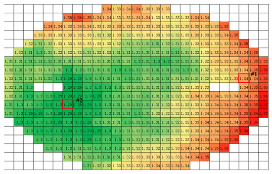
Figure 12.
The CP distribution of VF (IF = 20 A) on a wafer from the manuscript FRD.
The P+ implantation generates the anode region of the FRD, while the push-up process activates the boron and facilitates the formation of a PN junction. During this process, the entire wafer experiences technological warping, leading to varying influences of the push-up process across different locations on the wafer. As illustrated, a notable discrepancy in processing emerges between the lower-left and upper-right corners of the wafer, characterized by differing anode states. The anode region formed in the lower-left corner exhibits a higher concentration, resulting in a smaller VF, while the anode concentration near the upper-right corner is comparatively lower. Similarly, a denser anode region necessitates a greater extraction of carriers during the reverse recovery process, thereby correlating with a higher IRR. Moreover, this technological variance also adversely impacts the model’s predictions regarding reverse recovery characteristics. No model can afford to disregard the errors induced by the fabrication process itself.
As illustrated in Figure 13, two devices exhibiting significant variations in VF were selected for dual-pulse testing, followed by a comparative analysis with the predictive model. In fact, the observed process fluctuations do lead to potential discrepancies in the predictive model.
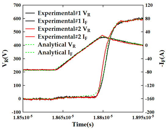
Figure 13.
A comparative analysis of dual-pulse test results for devices exhibiting significant variations in VF and their corresponding predictive models.
4.2. Comparison Between Analytical Model and the Lumped-Charge Model
As illustrated in Figure 14, compared to the lumped-charge model mentioned in [10], the advantages of the lumped-charge method are manifested in its high predictive accuracy once the voltage and current stabilize. However, this methodology exhibits certain limitations when addressing the impact of parasitic components in the system, particularly evident in the voltage waveform during the initial state, where the associated errors tend to be substantial. In comparison, the analytical model presented in this paper exhibits inferior accuracy near the peak current IRR relative to the lumped charge method yet demonstrates superior performance in forecasting the voltage waveform.
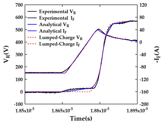
Figure 14.
Comparative of the predictions from the analytical model for FRD and the lumped-charge model.
The Root Mean Square Error (RMSE) is a widely used metric for assessing the deviation between predicted values and actual values. It is calculated by taking the square root of the sum of the squared differences between predicted values and actual values, normalized by the number of test currents. This method is particularly sensitive to outliers within the data, thus effectively reflecting the precision of the measurements. The RMSE is calculated using Formula (64):
As illustrated in Figure 15, the analysis of RMSE reveals that the new analytical model offers an improvement in accuracy when predicting the reverse recovery characteristics of FRD devices compared to the previous model mentioned in [10]. The predictive accuracy of IF utilizing the new model is comparable to that of the lumped charge method. Concurrently, the prediction accuracy of VR has also exhibited an enhancement of approximately 5%. This improvement underscores the new model’s capability to effectively capture transient voltage variation, thereby providing a more precise representation of the dynamic characteristics of voltage under diverse operational conditions.
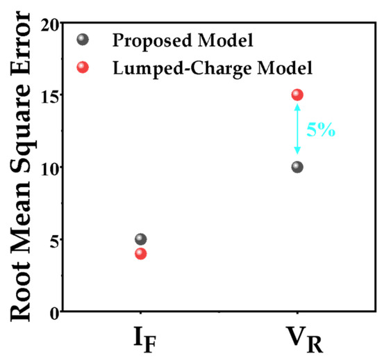
Figure 15.
Comparison of the accuracy between the new analytical model and the previous model.
The analytical model is based on the changes in different processes of reverse recovery, and the calculation of different processes is realized by formula deduction, and finally, the overall model is obtained. At present, the advanced lumped charge method uses node analysis and spice model calculation to fit. In terms of efficiency, the analytical model obtains reverse recovery characteristics through formula derivation and differential equation solving, while the lumped charge needs coupling node analysis and software calculation to be realized. The calculation power of simulation software is used, and the efficiency is significantly lower than that of the analytical model proposed in this paper.
4.3. Analytical Model Certification Under Different Test RG
By extending the test resistances to 5 Ω and 20 Ω, it can be observed from Figure 16 that the analytical model continues to predict the reverse recovery characteristics with considerable accuracy. When the test resistance is set to 5 Ω, a significant increase in the speed of IRR is clearly observable compared to previous measurements, resulting in a notable rise in IRR. Correspondingly, the rate of voltage increase also experiences a substantial enhancement. Additionally, it is noted that Error 2, as depicted in Figure 16b, diminishes when the resistance is set to 20 Ω. This reduction is attributed to the increased resistance, which leads to a slower turn-on rate, thereby significantly attenuating the dynamic response of the parasitic inductive components.
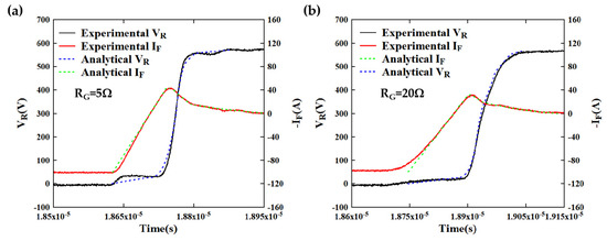
Figure 16.
Prediction of reverse recovery characteristics by the analytical model under different test RG (a) RG = 5 Ω; (b) RG = 20 Ω.
4.4. Analytical Model Certification Under Different VCC and IF
As illustrated in Figure 17, through a series of experimental tests involving varying bus voltages and currents, it has been demonstrated that the derived model can accurately predict the reverse recovery characteristics of the FRD. As the current is increased, the primary effect on the FRD is reflected in the variation of IRR. Specifically, at a constant rate of change in reverse recovery dI/dt, a higher current prolongs the time taken for the FRD to reach IRR while simultaneously resulting in an elevated IRR. In contrast, an increase in bus voltage primarily influences the fourth phase of voltage extension within the depletion region of the FRD. At this juncture, the FRD is required to endure an even higher voltage.
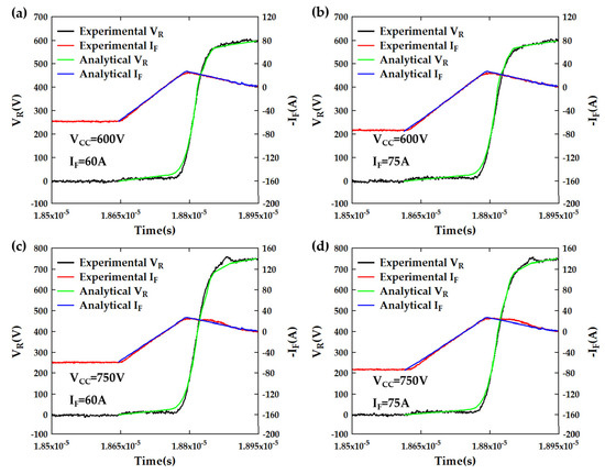
Figure 17.
Prediction of reverse recovery characteristics by the analytical model under different test VCC and IF. (a) VCC = 600 V, IF = 60 A; (b) VCC = 600 V, IF = 75 A; (c) VCC = 750 V, IF = 60 A; (d) VCC = 750 V, IF = 75 A.
4.5. Analytical Model Certification Under Different Temperature
It is well established that at high temperatures, carrier mobility diminishes while carrier lifetime increases, resulting in a degradation of reverse recovery performance. As illustrated in Figure 18, due to the maintenance of a consistent dIF/dt rate, the initial reverse recovery speed remains unchanged even at elevated temperatures. However, the IRR exhibits a marked increase at high temperatures, resulting in greater reverse recovery losses. Additionally, as temperature rises, carrier mobility diminishes, leading to a deceleration in the expansion of the depletion region. Consequently, the rate of voltage increase across the terminals of the FRD is slower than that observed at room temperature.
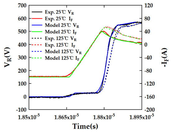
Figure 18.
Validation of the analytical model for reverse recovery through comparative experimentation at various temperature levels.
5. Conclusions
This paper constructs the carrier distribution in a PT-PIN FRD with a buffer layer under high injection conditions, delving into the physical properties of the materials, doping concentrations, and the geometric structure of the device. The FRD, in conjunction with its parallel IGBT, is predominantly employed in the realms of photovoltaics and energy storage, operating within a frequency range of 10 to 16 kHz. The relatively swift switching speed can, to a certain extent, induce oscillations in the waveform. Consequently, the significance of the PT-PIN FRD with a buffer layer resides in the adoption of a gentler reverse recovery characteristic, which allows for the prediction of reverse recovery waveforms, thereby circumventing issues such as reverse recovery oscillation.
The model is based on PN junction theory, where, under high injection conditions, the distribution of carriers no longer conforms to a linear approximation; instead, it necessitates consideration of the complex interplay between carrier recombination, diffusion, and drift. Through numerical simulations and analytical derivations, the spatial distribution of carrier concentration within the FRD under high current density conditions has been obtained. The analytical results for carrier distribution under high injection conditions allow for the characterization of the reverse recovery process through temporal segmentation, dividing the recovery into five distinct stages. This framework describes the dynamic transition of the diode from the conducting state to the cutoff state. Utilizing the analytical model, it is possible to derive crucial parameters such as reverse recovery time, reverse recovery current, and current slope. The experimental results indicate a significant enhancement in the accuracy of the analytical model when compared with previous models that employed the lumped-charge method. Furthermore, there has been an improvement in the voltage prediction accuracy relative to the most recent lumped-charge method. This model is capable of precisely forecasting the reverse recovery characteristics under varying test conditions of RG, VCC, and IF.
At present, this model does not include semiconductor-level device simulation similar to TCAD or circuit-level Spiec simulation. We hope to continue to expand this model in subsequent studies, especially for advanced hydrogen ion injection, helium ion injection, and other new technology life control methods, which are included in the calculation of the model. A wider range of applications has been achieved.
Supplementary Materials
The following supporting information can be downloaded at: https://www.mdpi.com/article/10.3390/electronics14030570/s1, Appendix: The derivation of Equation (5).
Author Contributions
Conceptualization, Y.S. (Yameng Sun); data curation, K.M., X.Y. and A.C.; formal analysis, Y.S. (Yameng Sun) and X.Y.; funding acquisition, Y.Z. and S.L.; investigation, X.L. (Xun Liu) and Y.S. (Yifan Song); methodology, K.M.; project administration, Y.Z. and S.L.; supervision, Y.Z. and S.L.; validation, K.M. and X.L. (Xuehan Li); visualization, T.Z.; writing—original draft, Y.S. (Yameng Sun); writing—review and editing, Y.S. (Yameng Sun). All authors have read and agreed to the published version of the manuscript.
Funding
This work was supported in part by the National Natural Science Foundation of China under Grant 51727901 and Grant U1501241, in part by the National Key Research and Development Program of China under Grant 2017YFB1103904, and in part by the Hubei Provincial Natural Science Foundation of China under Grant 2020CFA032.
Data Availability Statement
The original contributions presented in this study are included in the article/Supplementary Material. Further inquiries can be directed to the corresponding author(s).
Conflicts of Interest
The authors declare no conflicts of interest. Author Yameng Sun was employed by the company Hefei Archimedes Electronic Technology Co., Ltd. The remaining authors declare that the research was conducted in the absence of any commercial or financial relationships that could be construed as a potential conflict of interest.
References
- Wang, C.; Yin, L.; Wang, C. A physics-based model for fastrecovery diodes with lifetime control and emitter efficiency reduction. World Acad. Sci. Eng. Technol. 2012, 61, 7–11. [Google Scholar] [CrossRef]
- Bryant, A.; Lu, L.; Santi, E.; Hudgins, J.; Palmer, P. Modeling of IGBT resistive and inductive turn-on behavior. IEEE Trans. Ind. Appl. 2008, 44, 904–914. [Google Scholar] [CrossRef]
- Luo, Y.; Xiao, F.; Wang, B.; Liu, B.; Xia, Y. A voltage model of PIN diodes at reverse recovery under short-time freewheeling. IEEE Trans. Power Electron. 2017, 32, 142–149. [Google Scholar] [CrossRef]
- Mijlad, N.; Elwarraki, E.; Elbacha, A. SIMSCAPE electro-thermal modelling of the PIN diode for power circuits simulation. IET Power Electron. 2016, 9, 1521–1526. [Google Scholar] [CrossRef]
- Yamashita, Y.; Tadano, H. Numerical modeling of reverse recovery characteristic in silicon pin diodes. Solid-State Electron. 2018, 145, 8–18. [Google Scholar] [CrossRef]
- Karadžinov, Ĺ.; Jefferies, D.; Arsov, G.; Deane, J. Simple piecewise-linear diode model for transient behaviour. Int. J. Electron. 1995, 78, 143–160. [Google Scholar] [CrossRef]
- Jahdi, S.; Alatise, O.; Ran, L.; Mawby, P. Accurate analytical modeling for switching energy of PiN diodes reverse recovery. IEEE Trans. Ind. Electron. 2015, 62, 1461–1470. [Google Scholar] [CrossRef]
- Strollo, A. A new SPICE model of power PIN diode based onasymptotic waveform evaluation. IEEE Trans. Power Electron. 1997, 12, 12–20. [Google Scholar] [CrossRef]
- Shaker, A.; Abouelatta, M.; El-Banna, M.; Ossaimee, M.; Zekry, A. Full electrothermal physically-based modeling of the powerdiode using PSPICE. Solid-State Electron. 2016, 116, 70–79. [Google Scholar] [CrossRef]
- Li, X.; Luo, Y.; Duan, Y.; Huang, Y.; Liu, B. A lumped-charge model for high-power PT-p-i-n Diode with a buffer layer. IEEE J. Emerg. Sel. Top. Power Electron. 2019, 7, 52–61. [Google Scholar] [CrossRef]
- Li, X.; Xiao, F.; Luo, Y.; Wang, R.; Duan, Y. Modeling of high-voltage nonpunch-through PIN diode snappy reverse recovery and its optimal suppression method based on RC snubber circuit. IEEE Trans. Ind. Electron. 2021, 69, 5700–5712. [Google Scholar] [CrossRef]
- Jankovic, N.; Pesic, T.; Igic, P. All injection level power PIN diode model including temperature dependence. Solid-State Electron. 2007, 51, 719–725. [Google Scholar] [CrossRef]
- Benda, H.; Spenke, E. Reverse recovery processes in silicon power rectifiers. Proc. IEEE 1967, 55, 1331–1354. [Google Scholar] [CrossRef]
- Baliga, B.; Sun, E. Comparison of gold, platinum, and electron irradiation for controlling lifetime in power rectifiers. IEEE Trans. Electron Device 1977, 24, 685–688. [Google Scholar] [CrossRef]
- Takata, I.; Bessho, M.; Koyanagi, K.; Akamatsu, M.; Satoh, K.; Kurachi, K. Snubberless turn-off capability of four-inch 4.5 kV GCT thyristor. In Proceedings of the 10th International Symposium on Power Semiconductor Devices and ICs, Kyoto, Japan, 3–6 June 1998; pp. 177–180. [Google Scholar] [CrossRef]
- Xue, P.; Fu, G.; Zhang, D. Comprehensive physics-based compact model for fast pin diode using MATLAB and simulink. Solid-State Electron. 2016, 121, 1–11. [Google Scholar] [CrossRef]
- Ghandhi, S. Semiconductor Power Devices; Wiley: New York, NY, USA, 1977; pp. 112–128. [Google Scholar]
- Hall, R. Power rectifiers and transistors. Proc. IRE 1952, 40, 1512–1518. [Google Scholar] [CrossRef]
- Khaleqi Qaleh Jooq, M.; Miralaei, M.; Ramezani, A. Post-layout simulation of an ultra-low-power OTA using DTMOS input differential pair. Int. J. Electron. Lett. 2017, 6, 168–180. [Google Scholar] [CrossRef]
- Khaleqi Qaleh Jooq, M.; Mir, A.; Mirzakuchaki, S.; Farmani, A. A robust and energy-efficient near-threshold SRAM cell utilizing ballistic carbon nanotube wrap-gate transistors. AEU—Int. J. Electron. Commun. 2019, 110, 152874. [Google Scholar] [CrossRef]
- Ballga, J. Fundamentals of Power Semiconductor Devices; Springer: Berlin/Heidelberg, Germany, 2008; Volume 95. [Google Scholar]
- Carlson, R.; Sun, Y.; Assalit, H. Lifetime control in silicon power devices by electron or gamma irradiation. IEEE Trans. Electron Devices 1977, 24, 1103–1108. [Google Scholar] [CrossRef]
- Siemieniec, R.; Sudkamp, W.; Lutz, J. Determination of parameters of radiation induced traps in silicon. Solid-State Electron. 2002, 46, 891–901. [Google Scholar] [CrossRef]
- Siemieniec, R.; Lutz, J. Possibilities and limits of axial lifetime control by radiation induced centers in fast recovery diodes. Microelectron. J. 2004, 35, 259–267. [Google Scholar] [CrossRef]
- Onishi, H.; Shirai, H. Silicon ultrafast recovery diode with leakage current reduced via the combined lifetime process of gold diffusion and electron-beam irradiation. Semicond. Sci. Technol. 2024, 39, 015011. [Google Scholar] [CrossRef]
Disclaimer/Publisher’s Note: The statements, opinions and data contained in all publications are solely those of the individual author(s) and contributor(s) and not of MDPI and/or the editor(s). MDPI and/or the editor(s) disclaim responsibility for any injury to people or property resulting from any ideas, methods, instructions or products referred to in the content. |
© 2025 by the authors. Licensee MDPI, Basel, Switzerland. This article is an open access article distributed under the terms and conditions of the Creative Commons Attribution (CC BY) license (https://creativecommons.org/licenses/by/4.0/).