Article

Simple Planar Microstrip Crossover Coupler with Independent Control over Bandwidth and Selectivity

1
Laboratory of Systems and Communication Engineering, Grenoble Institute of Technology, 26902 Valence, France
2
Electrical and Computer Engineering Department, Faculty of Engineering, Beirut Arab University, Debbieh 1504, Lebanon
*
Author to whom correspondence should be addressed.
Electronics 2025, 14(23), 4737; https://doi.org/10.3390/electronics14234737
Submission received: 29 October 2025 / Revised: 24 November 2025 / Accepted: 26 November 2025 / Published: 1 December 2025
(This article belongs to the Section Electronic Materials, Devices and Applications)

Abstract

This paper presents the design, optimization, and measurement validation of a highly compact and frequency-selective Microstrip Crossover architecture for microwave applications, specifically targeting the 2.4 GHz band. The proposed design features a modified hexagonal structure enhanced with Sierpinski carpets, four loading stubs on the access lines, and Defected Ground Structures (DGS), along with two via holes to excite a new operating mode. This integration achieves an outstanding miniaturization ratio, occupying 62% less surface area compared to conventional crossover designs. Through simulation, the optimized structure demonstrates superior performance with low insertion loss of 1 dB and Isolation/Matching better than 20 dB at 2.4 GHz. A key contribution is the demonstrated response controllability, where the loading stubs and DGS serve as independent tuning elements: the stub length controls the frequency of the lower band transmission zeros for selectivity control, while the DGS dimensions govern the passband width and Fractional Bandwidth (FBW).

1. Introduction

Couplers are fundamental and ubiquitous components in modern wireless communication systems. Among them, the crossover coupler is particularly critical, finding extensive applications in base stations, radar systems, satellite payloads, and various other communication platforms. A crossover coupler is a four-port directional component designed to allow two independent transmission lines to intersect on the same physical layer without significant coupling, interference, or signal degradation. Specifically, it enables a signal entering Port 1 to transmit to Port 3, and a signal entering Port 2 to transmit to Port 4, while maintaining high isolation between the two crossing paths (Ports 1 and 2, Ports 3 and 4, etc.). Its primary function is to simplify complex circuit routing by avoiding the need for multi-layer structures, air bridges, or via holes in the signal path, thereby reducing fabrication complexity and cost. Crossovers are essential for planar integrated circuit design, as they manage signal–path crossings, thereby eliminating the need for complex, costly, multilayer structures like air bridges.
The design of planar crossovers traditionally relies on simple structures such as microstrip lines [1], branch-line couplers [2], or specialized microstrip patches [3]. While these conventional approaches offer simplicity in fabrication, they inherently suffer from two major drawbacks that limit their utility in high-performance systems: large physical size and poor electrical performance (e.g., narrow bandwidth, low isolation, or high insertion loss).
The recent literature on planar and waveguide crossovers reveals a broad spectrum of design methodologies targeting concurrent improvements in compactness, bandwidth, and signal integrity. Ring resonator-based designs [4,5,6] have been extensively investigated for balanced operation, employing even–odd mode analysis to achieve excellent differential mode isolation and return loss while maintaining structural symmetry. Complementary to these, slot- and patch-based geometries—including Γ-shaped, arc-shaped, and formula-inspired slots—have demonstrated remarkable miniaturization and bandwidth enhancement [7,8,9], achieving up to 71% area reduction compared to conventional structures, without compromising isolation (>19 dB) or insertion loss (<1 dB). For broadband beamforming networks, coupled-line and multi-section branch-line crossovers [10] have been effectively utilized within Butler matrices, providing wide operational bandwidths (2.1–2.75 GHz) with isolation exceeding 30 dB. In parallel, Substrate Integrated Waveguide (SIW)-based designs [11,12] have emerged as a powerful alternative, leveraging multimode orthogonality (TE102/TE201) and 3D stacking to achieve low insertion loss (~1 dB) and high port isolation (>35 dB) suitable for high-power and beamforming applications. Furthermore, filter-integrated architectures, such as balanced-to-balanced (BTB) filtering crossovers [13], have demonstrated exceptional common mode suppression (>45 dB) and differential mode isolation (~43 dB), thereby unifying crossover and filtering functions in a single planar structure. Collectively, these diverse approaches underline the evolution from conventional microstrip layouts toward compact, high-isolation, and multifunctional crossovers, yet achieving simultaneous ultra-wideband operation, extreme miniaturization, and minimal loss remain key challenges motivating ongoing research.
This work introduces a novel, compact, hexagonal crossover realized through the strategic integration of an optimized Defected Ground Structure (DGS) topology and reactive loading stubs. The primary originality and technical contribution lie in the development of a unique control technique: the DGS is engineered to independently control the Fractional Bandwidth (FBW), while the loading stubs are dedicated to managing the circuit’s selectivity by creating highly tunable transmission zeros. This combination yields a device that achieves exceptional miniaturization (occupying 62% less surface area than conventional structures), exhibits high port isolation, and presents a significant leap forward in designing highly customizable and integrated planar microwave circuits.
The remainder of this paper is organized as follows: Section 2 details the design requirements for a compact crossover device and the basic design used. Section 3 presents the modified compact hexagonal crossover design incorporating Sierpinski and DGS techniques, detailing subsequent structural refinements including the introduction of a lower band transmission zero and grounded via holes. Section 4 introduces the Response-Controlled Compact Hexagonal Crossover, discussing the role of loading stubs for selectivity control and DGS for FBW Control. Section 5 presents the measurement results, validating the superior performance of the proposed design. Finally, Section 6 presents a discussion of the results.

2. Materials and Methods

2.1. Design Requirements

Conventional microstrip crossovers often suffer from limitations such as large size and suboptimal performance characteristics. This work aims to address these shortcomings. The proposed four-port crossover is targeted for operation at a center frequency of 2.4 GHz. The key design requirements are as follows:
  • Excellent Port Matching: All ports must be well-matched to 50 Ω within the operating band to minimize signal reflections and ensure maximum power transfer.
  • Low Insertion Loss: The through paths must exhibit low insertion loss to ensure minimal signal attenuation as signals transit the crossover.
  • High Isolation: A critical requirement is to achieve high isolation between the two independent signal paths and across all non-transmitting ports. This minimizes crosstalk and ensures signal integrity.
  • Compact Physical Footprint: The crossover must be significantly smaller than conventional designs to meet the miniaturization demands of contemporary circuits and systems.
  • Defined Operating Bandwidth: The component must meet the specified performance criteria (matching, insertion loss, and isolation) over a defined fractional bandwidth (8–10%) centered at 2.4 GHz.
  • Enhanced Out-of-Band Rejection: The design should effectively suppress unwanted signals and harmonics outside the intended operating frequency range, contributing to overall system electromagnetic compatibility.
  • Simple: The design should be realized using planar microstrip technology, leveraging its advantages in terms of ease of fabrication and integration.
Meeting these requirements will lead to a crossover that is not only compact but also offers the outstanding electrical performance necessary for demanding applications, aligning with the trend towards more integrated and efficient wireless systems.

2.2. Full-Wave Simulation Environment

All design, optimization, and simulation validation were performed using the commercial full-wave electromagnetic simulator, Ansys HFSS (High-Frequency Structure Simulator). To ensure validation and reproducibility of the numerical results, the key solver settings used were as follows:
  • Frequency Range: Simulations were conducted across the range of 1.5 GHz to 3.0 GHz to capture the full passband and out-of-band rejection characteristics.
  • Port Excitation: All four ports of the crossover were excited using 50 Ohm wave-ports.
  • Boundary Conditions: The structure was enclosed within an air box defined by an open radiation boundary condition, placed at a minimum distance of λ/4 (one quarter wavelength at the lowest frequency) from the edges of the structure.
  • Mesh Settings: An adaptive tetrahedral mesh was employed across the entire structure and substrate volume.
  • Convergence Criteria: The Delta S-parameter convergence criterion was set to 0.02, with a maximum limit of 20 adaptive passes to achieve sufficient accuracy in the S-parameter results and a minimum of two successive converged passes.

2.3. Compact Hexagonal Crossover with Serpenski and DGS

In this section, we present the design of a hexagonal crossover that operates at 2.4 GHz. The substrate used is Rogers 4003C (Rogers Corporation, Chandler, AZ, USA) with a height h = 0.5 mm, copper thickness of 35 μm, a relative permittivity of εr = 3.38, and a loss tangent tan δ = 0.0027. This substrate is widely used in the design of microwave devices since it is of good quality, excellent stability, and offers low dielectric loss, which is helpful in our design.
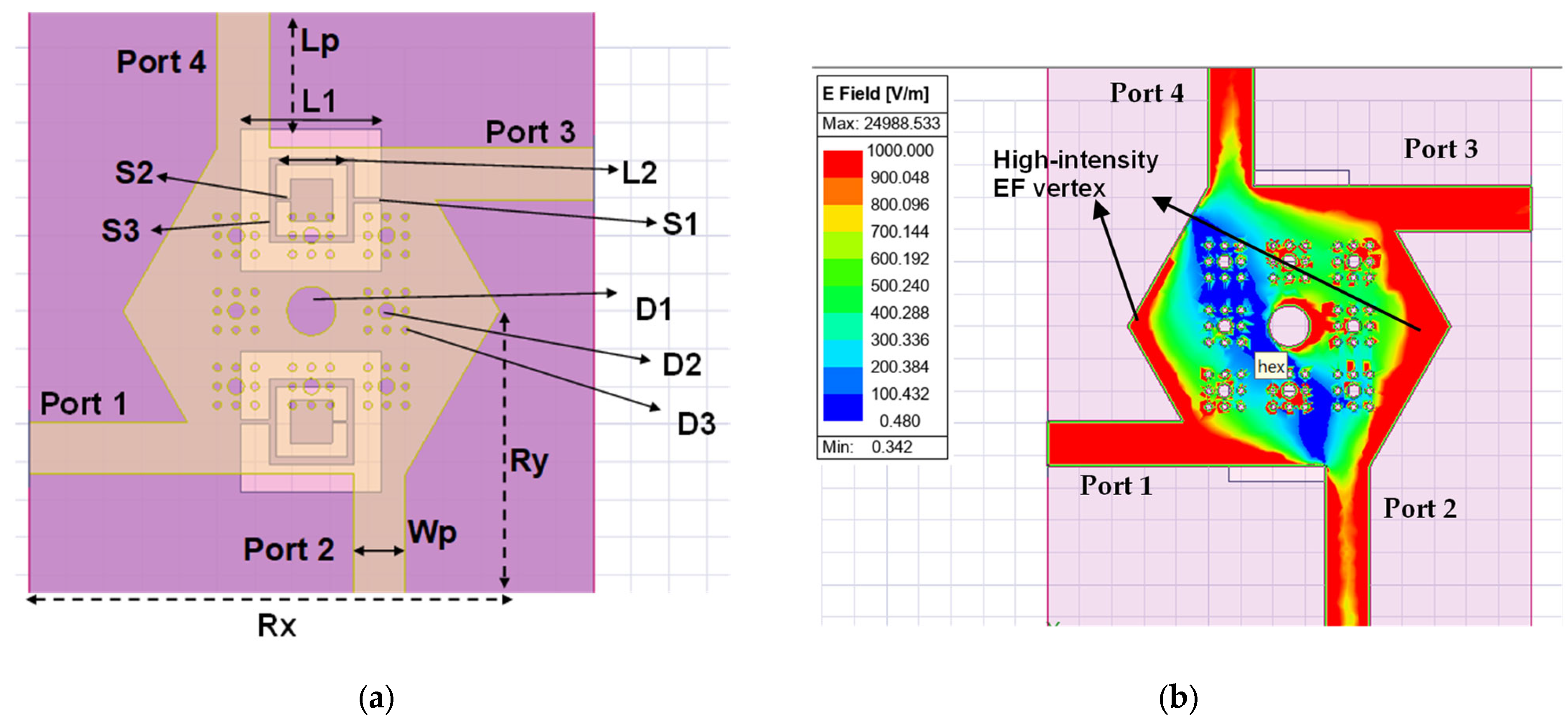
A classical hexagonal crossover, shown in Figure 1a, is composed of four ports (1 to 4) [14]. The hexagonal geometry was chosen over traditional square or circular patches due to its inherent advantages in four-port crossover design. The six-sided shape provides superior port separation and symmetry, which is critical for achieving high isolation between the two crossing signal paths (Port 1–3 and Port 2–4). Furthermore, the specific shape and larger perimeter of the hexagon, compared to a compact square patch, are more conducive to exciting the dominant mode while still offering a better starting point for miniaturization via the subsequent fractal and DGS etching. Rx and Ry define the dimensions of the crossover. A crossover is supposed to transmit a signal from port 1 to 3 and port 2 to 4 with minimum losses and interference. The transmission from port 1 to ports 2 and 4 should be minimal (the same as for that from port 2 to ports 1 and 3). This undesired transmission is known as isolation. The scattering parameters together with electric field intensity plots will be used to characterize the performance of the designed crossovers in this paper. A well-designed crossover is one that performs the desired transmission with minimum insertion loss, good port matching, and maximum isolation. Ideally, the insertion losses (S31 and S42) are equal to 1 (or 0 dB) at the operating frequency. On the other hand, the port matching (return loss) S11 is ideally equal to zero (or -infinity dB) and the isolation values (S21, S41, S32, and S12) are ideally equal to 0 (or -infinity dB) at the operating frequency.
Now, we will consider that the signal is injected into port 1 (the input port). The output port is port 3. Ports 2 and 4 will be referred to as the isolated ports.
The crossover should present equal signal characteristics at the desired output ports 3 and 4 when the signal is injected at ports 1 and 2, respectively. For better graph readability and to ensure that the crossover achieves this important criterion, we will present the phase imbalance and amplitude imbalance between the signals at the outports rather than plotting all the S-parameters. The phase imbalance shows the phase difference between the signals at the output ports 3 and 4 when the signal is injected at the input ports 1 and 2, respectively. The amplitude imbalance, on the other hand, presents the difference in amplitude between the signals at the output ports. Ideally, these two values should be null within the operating band. However, in practical cases, this is far from being true.
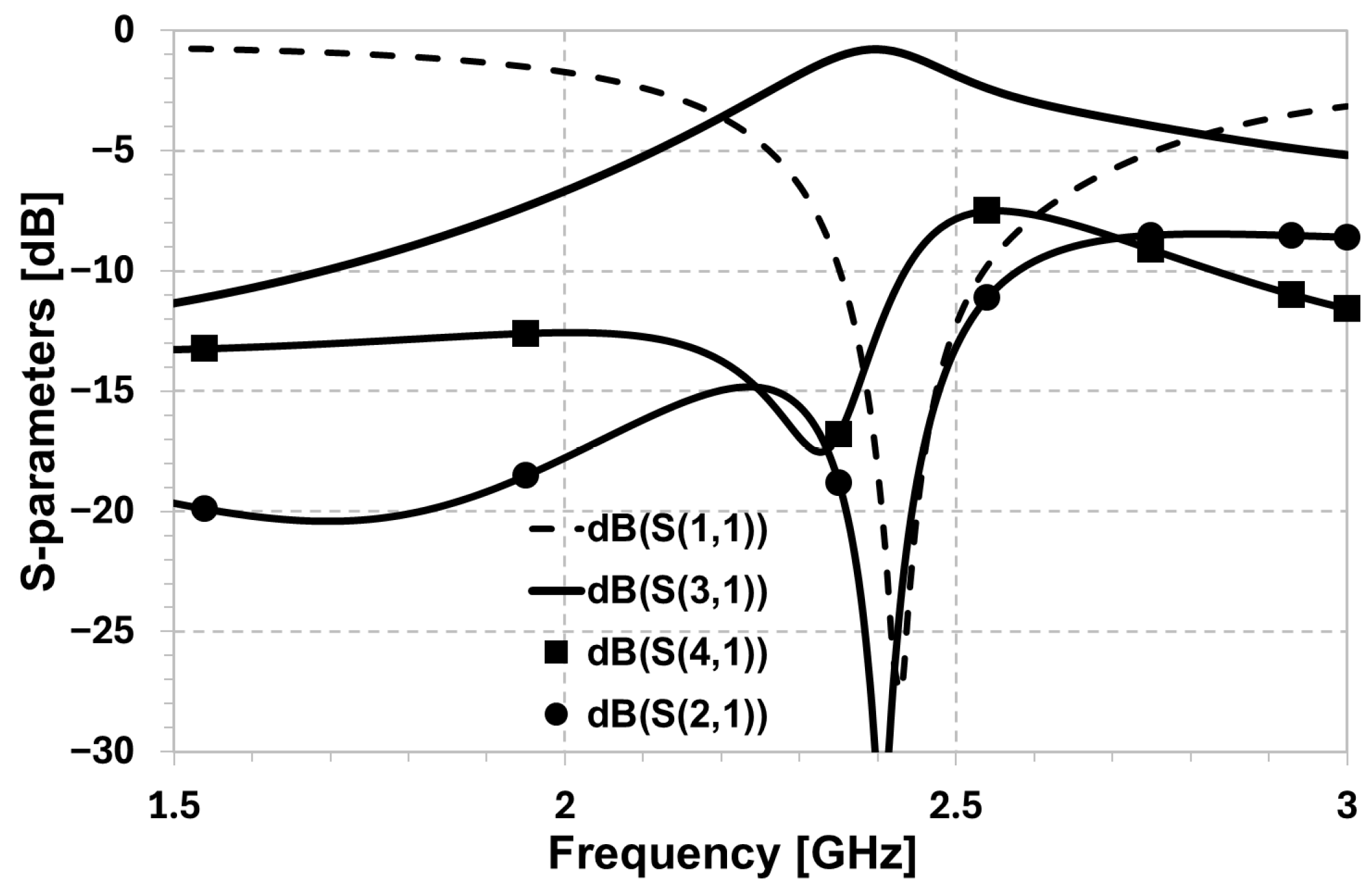
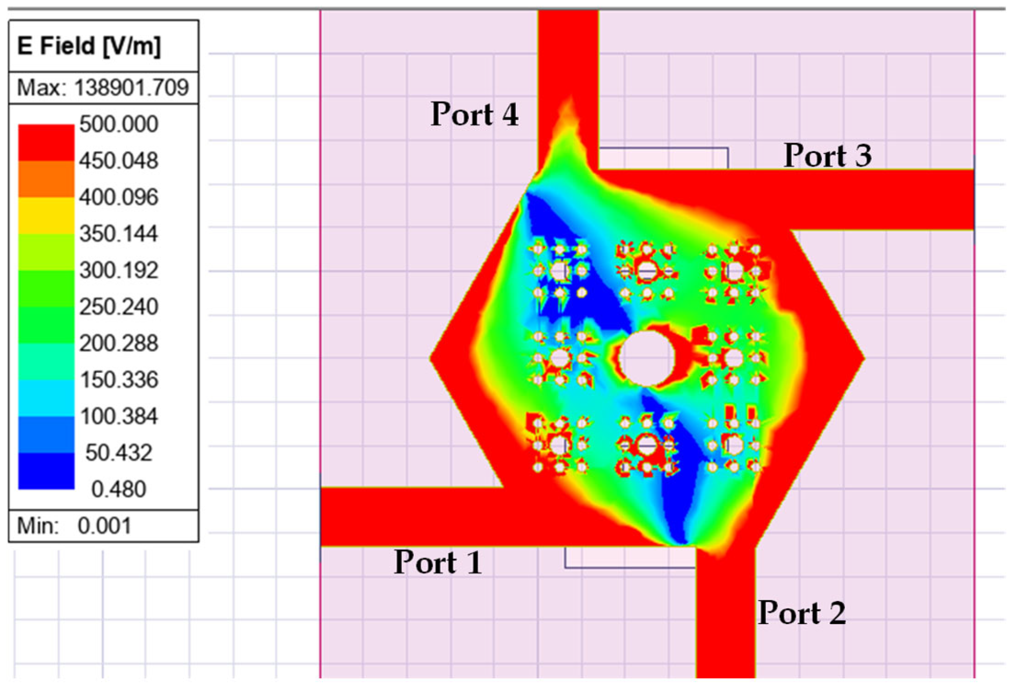
The classical hexagonal crossover is designed on the chosen substrate. The dimensions are Rx = 46.5 mm, Ry = 48.5 mm, Lp = 33.5 mm, and Wp = 2.75 mm. The classical crossover occupies a large area of (51.5 × 97) mm2. The electric field (EF) intensity plot at the operating frequency 2.4 GHz is shown in Figure 1b. The plot corresponds to a signal injected into port 1. The red color signifies that the EF intensity is maximum at the corresponding locations. On the other hand, the blue color signifies that the EF intensity is minimum at these locations. Figure 1b shows that the signal is being effectively transmitted from port 1 to 3 while a small portion of the signal barely reaches the isolation ports. The S-parameter results, shown in Figure 2, confirm the electric field plot shown in Figure 1b. At the design frequency of 2.4 GHz, the crossover exhibits a good insertion loss of 0.8 dB and a good return loss S11 better than 20 dB. On the other hand, the isolation at ports 2 and 4 (S21 and S41) is not optimum (12 dB). The large surface area is one more disadvantage of classical patch crossovers. Moreover, the bandwidth is high (0.5 GHz) and cannot be controlled with the current topology. The transmission coefficient S31 presents shallow slopes in the upper and lower rejection bands. This means that the crossover ability to reject the transmission of neighboring undesired frequencies is weak. Usually, this characteristic is referred to as selectivity. In most cases, it is preferable to have high selectivity.
To enhance the performance of the classical crossover and overcome its disadvantages, circular Sierpinski carpets of the third order are etched on the hexagonal crossover (upper copper layer) as shown in Figure 3a. The circular carpets have the diameters D1 (1st iteration, largest circles), D2 (2nd iteration, defined as D2 = D1/3), and D3 (3rd iteration, defined as D3 = D2/2). The Sierpinski carpets are primarily used for miniaturization and mode perturbation. The initial diameter, D1, is chosen heuristically to occupy approximately 5% of the shortest dimension of the hexagonal patch (Rx or Ry), ensuring a balance between miniaturization and excessive radiation loss. The subsequent diameters, D2 and D3, are determined by the fixed recursive simple factors (D1/3 and D2/2, respectively) to enhance the multi-level effects of the fractal geometry. Afterwards, the value was optimized for best performance (D1 = 2.6 mm).
In addition, two Split-Ring Resonator Defected Ground Structures (DGSs) are etched from the ground plane. The DGSs consist of two concentric square Split-Ring Resonators (SRRs), introduced primarily to create a high-frequency transmission zero for enhanced selectivity. The initial length of the outer SRR, L1, is guided by the principle that its perimeter (4L1) should correspond to roughly one-half wavelength (λ/2) at the desired zero frequency (approximately 2.9 GHz). This would yield L ≅ 2.9 mm. The size is then fine-tuned through full-wave simulation to precisely place the transmission zero and achieve the best Fractional Bandwidth (FBW) control (later on). The inner resonator (L2) adds capacitance for further coupling control. The dimension is chosen to always be L2 = L1/2 to keep the structure simple. The outer (larger) ring resonator has a width W1 and a gap S1, and the inner one has W2 = (W1)/2 and S2 = (S1)/2. The initial width W1 of the outer SRR is guided by setting it to the width of a 50 Ohm transmission line (W1 = 1.1 mm) and then fine-tuned through full-wave simulation. The Sierpinski fractal and the DGS will help reduce the hexagonal patch size and enhance its isolation and selectivity properties.
The crossover is designed on the same substrate as the classical one. The different dimensions are shown in Table 1. The overall size of the patch is 30 × 52 mm2. This means that this compact structure occupies about 69% less area than the classical one. The electric field plot when the input is on port 1 is shown in Figure 3b. The plot confirms that the signal is transmitted to the desired output port (port 3) effectively. The relatively non-negligible intensity of the field at the other ports (2 and 4) assumes that the isolation is weak, at 2.4 GHz. It is clear from Figure 3b that the electric field in the hexagonal region is concentrated in the left and right vertices. In the next section, we will use this to our advantage.
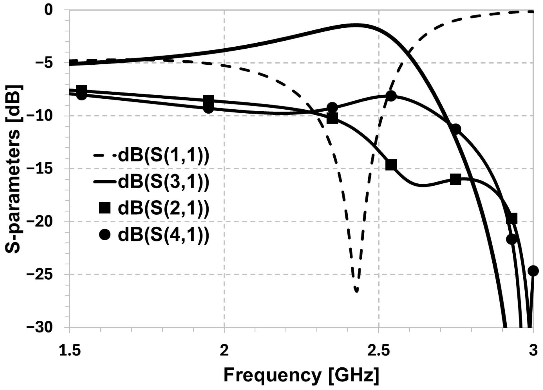
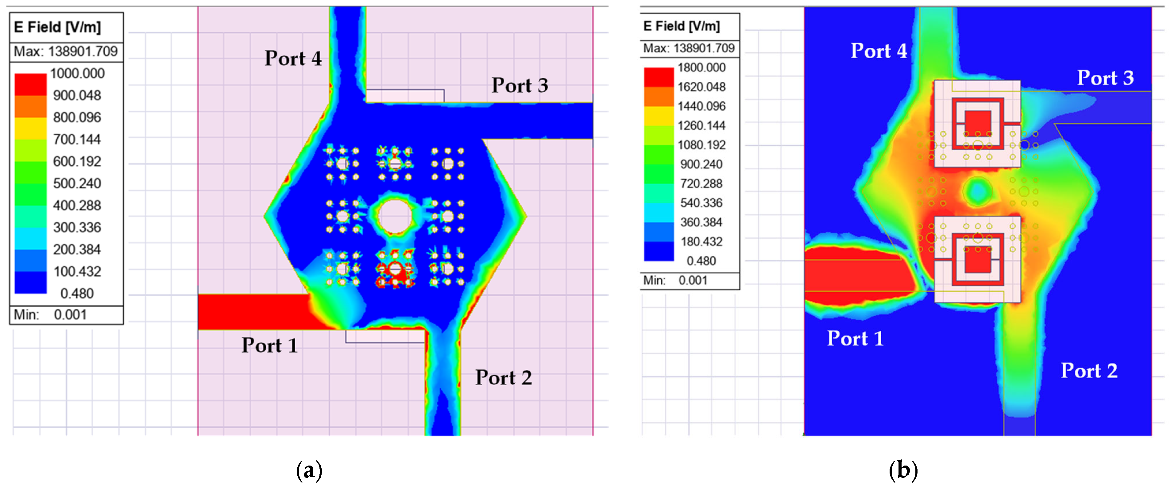
This electric field plot result is confirmed by looking at the S-parameter plot in Figure 4. The crossover is matched with a good return loss of 23 dB at 2.4 GHz. As for the selectivity, we notice that it is much better in the higher band. This is due to the transmission zero created by the inserted DGS elements. Figure 5 shows the electric field plot at the transmission zero frequency (2.9 GHz) in the top layer (Figure 5a) and in the ground plane where the DGSs are etched (Figure 5b). It is clear that at this frequency the signal does not reach any of the other ports, since the energy is trapped by the DGS. This transmission zero has the advantage of not only enhancing the selectivity but also the band controllability of the crossover, as we will show in the next subsection.
On the other hand, the insertion loss at the operating frequency is found to be 1.47 dB, which is higher than that for the classical crossover (0.8 dB). This is mainly due to the insertion of the Sierpinski carpets. The isolation at ports 2 and 4 is poor (9 dB). This means that there is still a non-negligible part of the signal that is being transmitted to the undesired output ports.
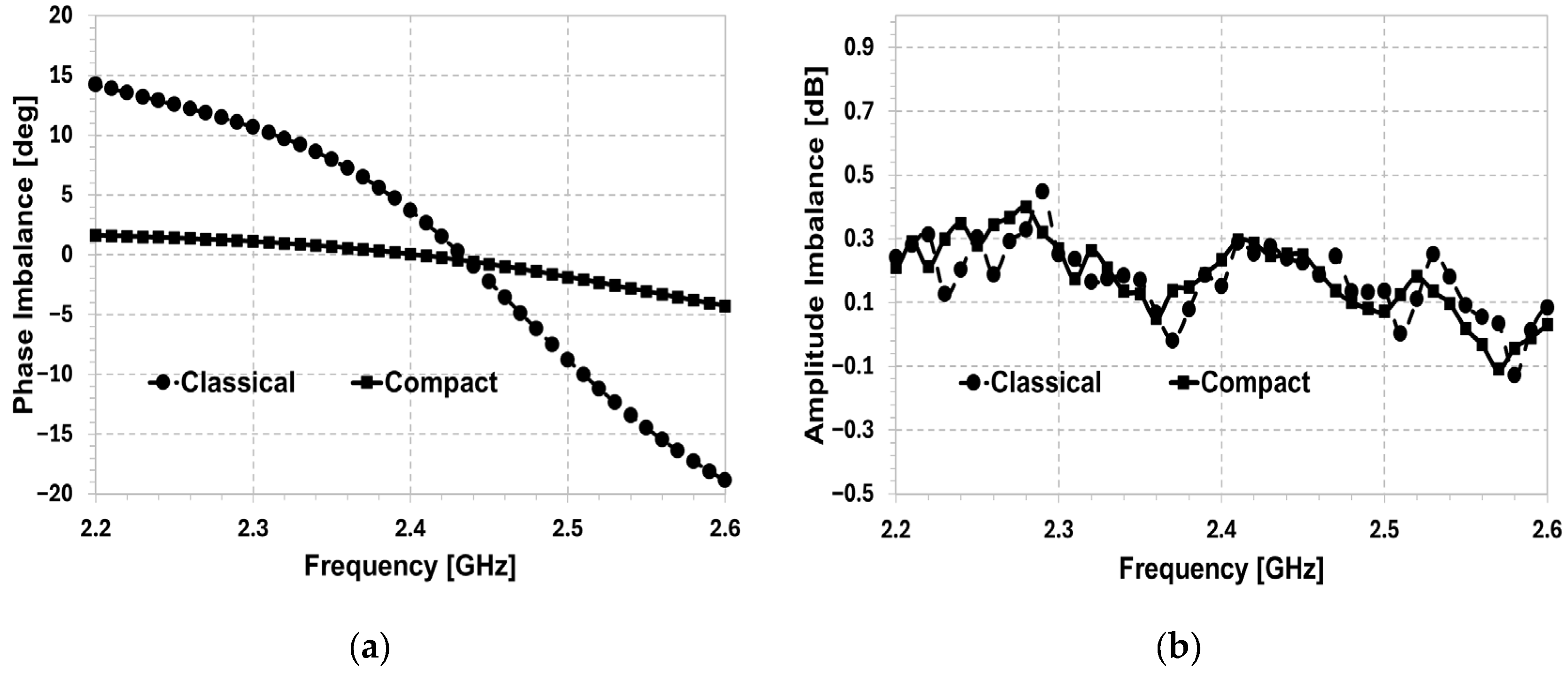
To ensure the symmetric operation of the crossover, the phase and amplitude imbalances between the output ports 3 and 4 when the inputs are placed on ports 1 and 2, respectively, are plotted in Figure 6. The imbalances for both the classical and compact crossovers are compared. The phase imbalance (PI) at the operating frequency is around 0 degrees for both designs. Around the operating frequency, the compact design performs better than the classical design. The compact crossover PI remains less than 6 degrees in the passband while that of the classical design is around 33 degrees. The compact design achieves a slightly improved amplitude imbalance (AI), tracking closely with the classical version but consistently remaining below 0.4 dB.
These results highlight the performance superiority of the proposed compact design. However, the crossovers still have low selectivity in the lower rejection band, high insertion loss, and poor isolation. In the next subsection we will be focusing on solving these disadvantages.

3. Modified Compact Hexagonal Crossover

The hexagonal crossover designed in the previous section still suffers from low selectivity, high losses, and poor isolation. To tackle these issues, one solution is to create transmission zero in the lower rejection band, at 1.8–1.9 GHz for example. This would enhance the selectivity of the crossover. In addition, to tackle the insertion loss issue, one solution is to create a new mode close to the operating frequency. This will make the passband flat and decrease the insertion loss around the operating frequency. A new mode can be triggered by placing a grounded via hole in the region where the electric field is high.

3.1. Lower Band Transmission Zero

Figure 7 shows the distribution of the EF intensity of the compact crossover around 1.9 GHz. It is clear that high transmission exists to all ports, which is undesirable. If we place a transmission zero at this frequency, the selectivity and the isolation can be enhanced.
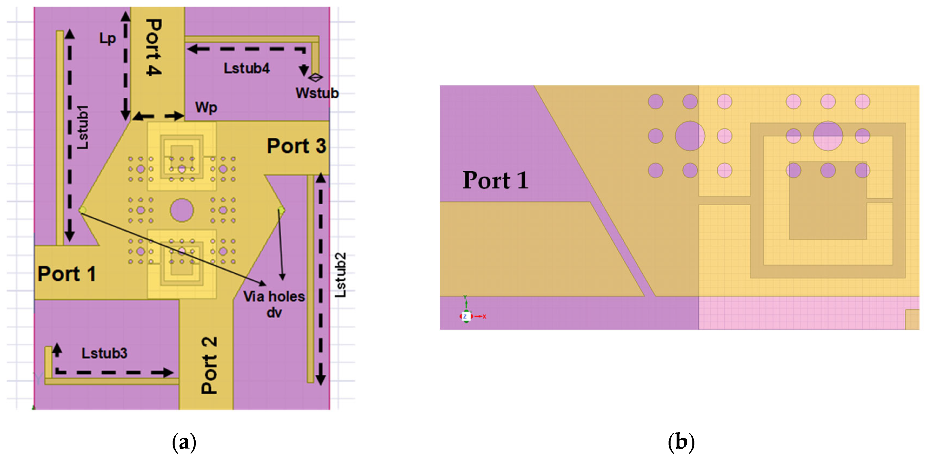
In order to create this transmission zero, an open-circuit shunt stub can be used to load the input port (stub 1 in Figure 8a) [15]. The stub length (Lstub1) can be optimized so that at 1.9 GHz the signal entering stub 1 will travel through it, reflect at its end (open-circuit), and travel back towards port 1. When it reaches back to the input port 1 it will be out of phase with the original signal, hence creating a transmission zero at 1.9 GHz. Lstub1 will define the exact frequency of the zero. Because we need the crossover to be symmetric, stubs 2, 3, and 4 are added at ports 2, 3, and 4, respectively (Figure 8a).

3.2. Grounded via Holes

As explained earlier, exciting another mode near the original dominant patch mode helps obtain a flat response (S31) in the passband. Mode perturbation can be achieved using via holes connected to the ground [16]. The placement of the grounded via holes is a strategic technique used to perturb the dominant resonant mode of the microstrip patch and excite a new one, which is essential for improving passband flatness and reducing insertion loss. According to fundamental perturbation theory, to achieve the maximum frequency shift and mode splitting, the via must be located where the unperturbed electric field (E-field) intensity is highest. For the hexagonal patch, this corresponds to the vertices (as visually confirmed in Figure 3b). By connecting the patch to the ground plane at these high-intensity points, the via acts as an efficient short circuit, severely disrupting the local E-field. This perturbation effectively splits the original mode, resulting in two closely spaced resonant modes that interact to flatten the frequency response. To understand this better, we plot the resonance frequencies of the hexagonal patch crossover with via places. An effective plot is achieved when the ports are faintly excited. This is achieved by creating a gap of around 0.3 mm at the connection points of all the ports with the hexagonal patch. A zoom on one of the ports is shown in Figure 8b.
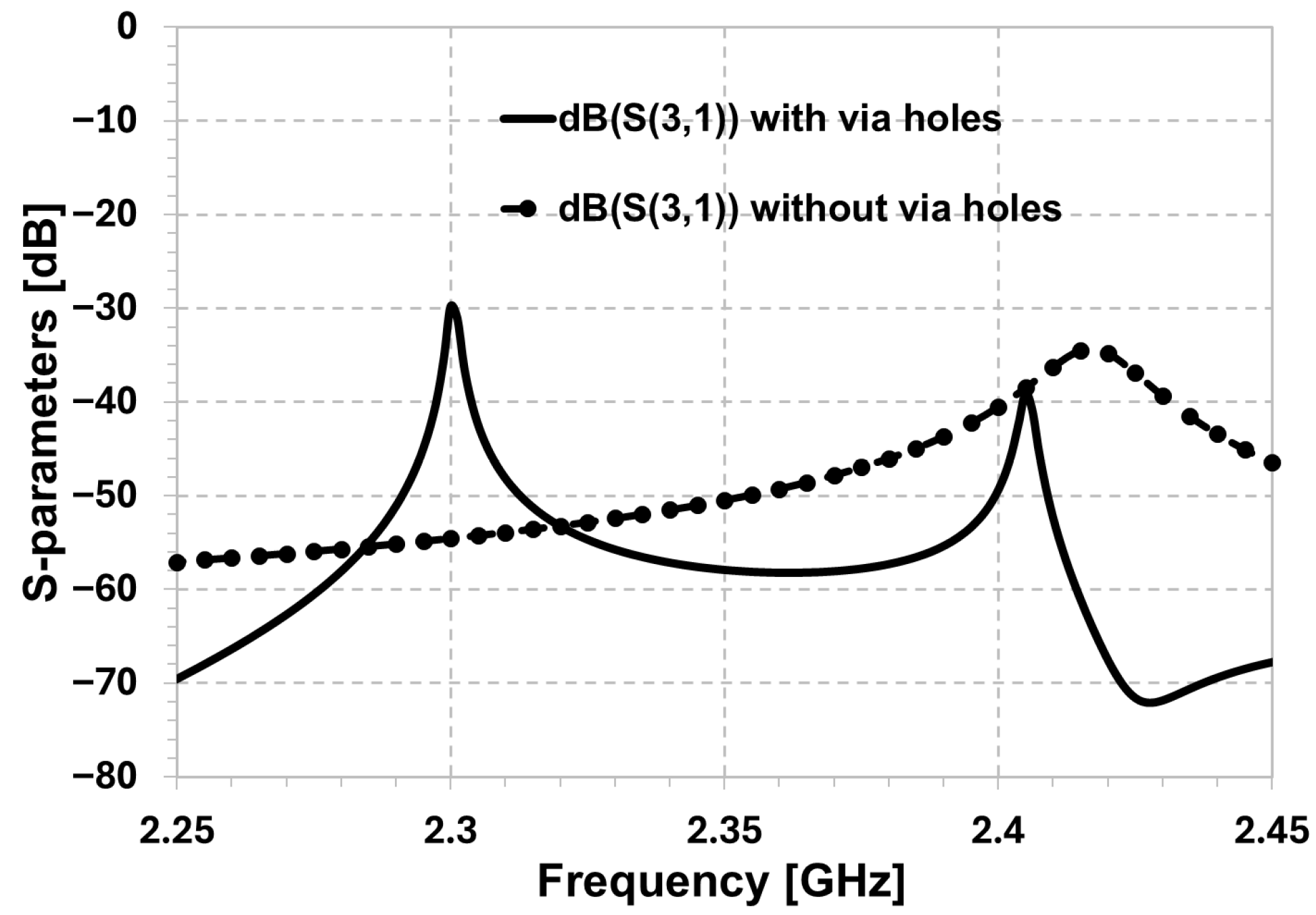
The transmission parameter S31 plot will show the resonance frequencies of the structure. Figure 9 shows the S31 plot versus frequency for two different weakly fed crossovers, one with via holes connected at the hexagon extremities and one without the presence of the via holes. As expected, the weakly fed crossover with no via holes has its dominant mode at about 2.415 GHz. On the other hand, when the via holes are added, a new mode is excited at 2.3 GHz, as shown. These two modes will be used to design the modified version of the compact hexagonal crossover.

3.3. Modified Crossover

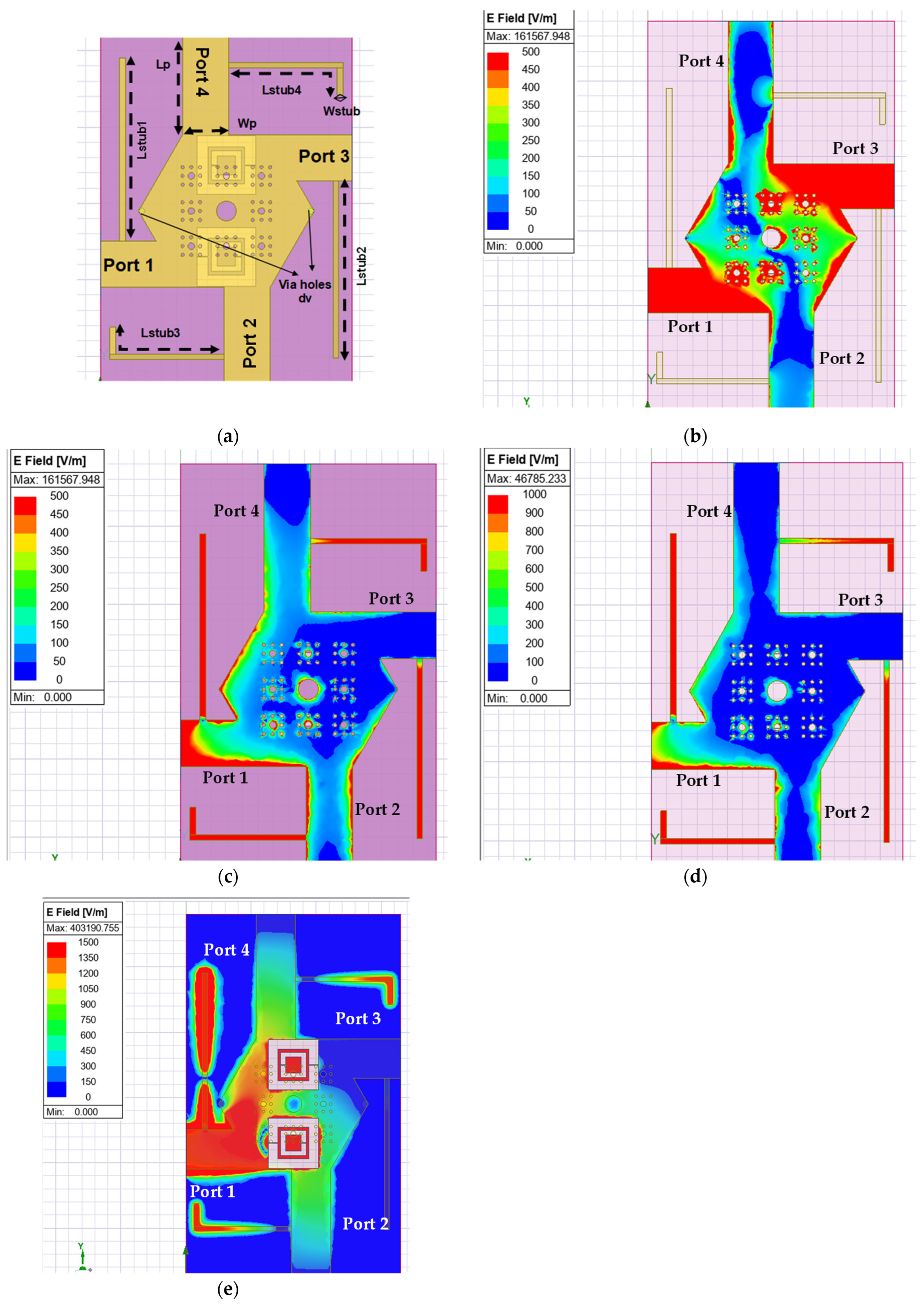
The modified design is shown in Figure 10a. This design incorporates two via holes added to excite a new mode. The via holes are plated through holes (PTHs) with copper plating and have diameters dv = 0.8 mm. The structure also includes identical stubs (stubs 1 to 4) at the input of its four ports. The loading stubs are placed around the middle of the access lines and have length Lstubi (i = 1 to 4) and width Wstubi.
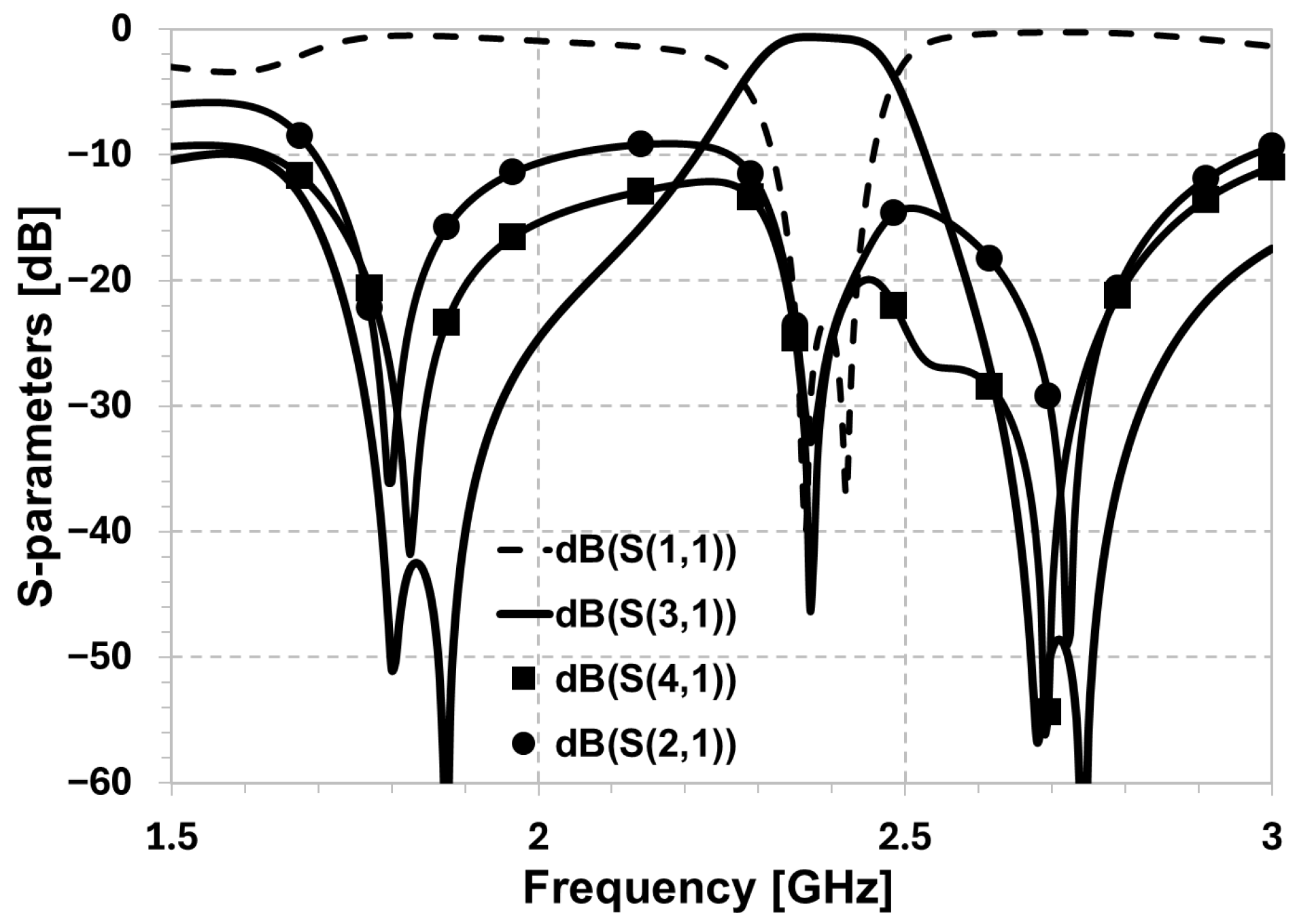
The structure is optimized for best performance. The dimensions are listed in Table 2. The modified compact crossover has a total dimension of 33 × 58 mm2. The total area of the modified compact crossover is almost the same as the previous design. Compared to a classical crossover design, the modified design occupies 62% less surface area. The electric field distribution when the input is on port 1 is shown in Figure 10b. The plot confirms that the signal is transmitted to the desired facing port effectively. The relatively negligible intensity of the field at the other ports (2 and 4) assumes that the isolation is good at 2.4 GHz. This is confirmed by the S-parameter plot in Figure 11. The response shows good matching and selectivity at the lower and higher bands. Moreover, the insertion loss at 2.4 GHz is 0.7 dB. This value is much better than the previous one of 1.47 dB. In addition, the isolation and matching are better than 25 dB around the operating frequency. The selectivity at the lower and higher rejection sides of the bandpass is high due to four transmission zeros (two in the lower rejection band and two in the upper one). Figure 10c,d show the effectiveness of the loading stubs in creating two closely separated transmission zeros in the lower rejection band. At fz1 = 1.81 GHz and fz2 = 1.89 GHz, stubs 1 and 2 introduce transmission zeros that prevent signal transmission to port 3. On the other hand, the DGS introduces a transmission zero by trapping the energy at fz3 = 2.75 GHz, as shown in Figure 10e. The fourth transmission zero at fz4 = 2.74 is created by stubs 3 and 4. The transmission zero frequencies created can be easily controlled by varying the dimensions of the stubs and the DGS. The following subsection presents a parametric study of these loading elements to investigate the possibility of controlling the band.

4. Response-Controlled Compact Hexagonal Crossover

In this subsection, a parametric study on the physical dimensions of the loading elements is conducted to determine the possibility of controlling the passband of the crossover.

4.1. Loading Stubs: Selectivity Control

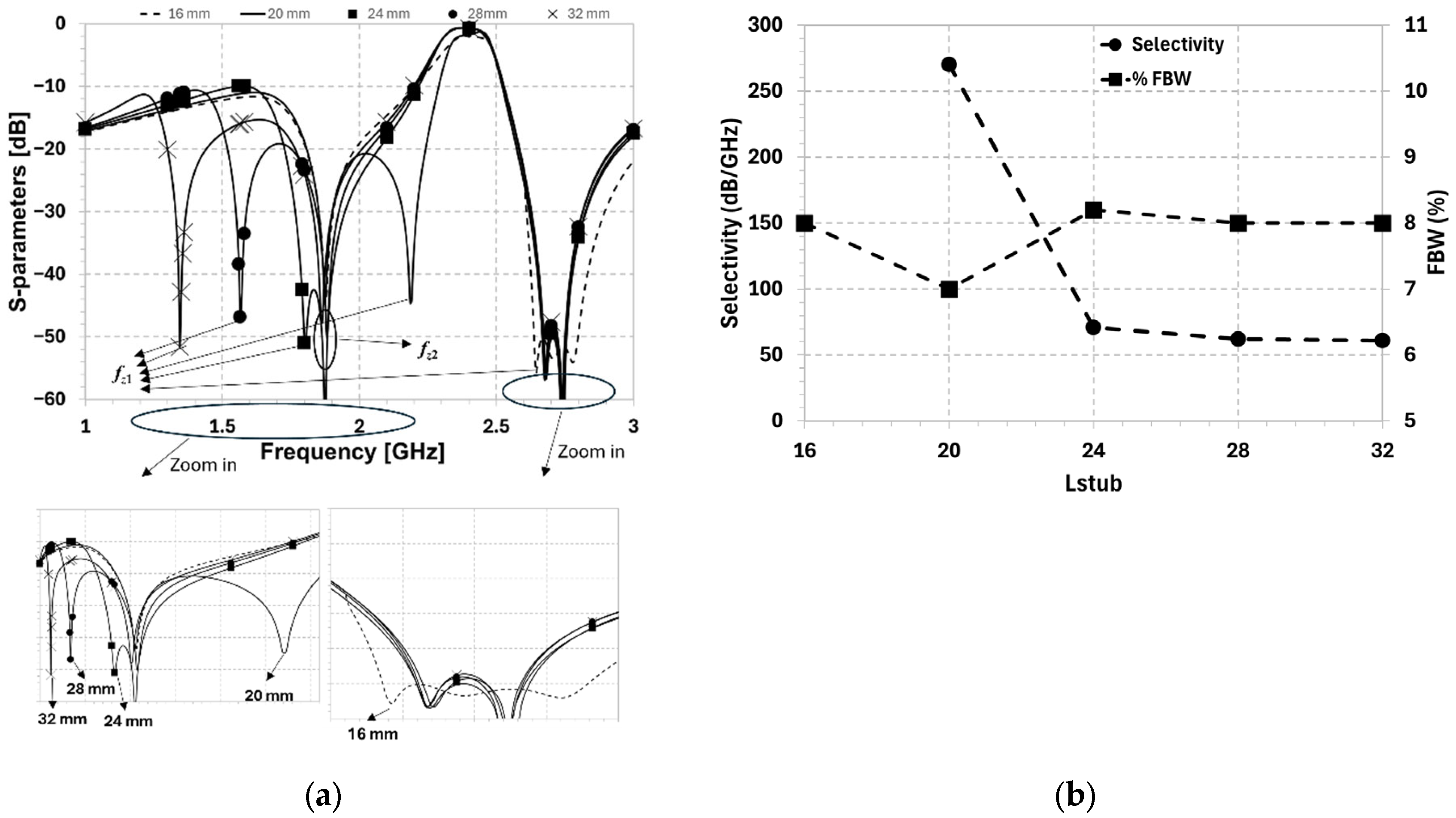
The lengths Lstub1 of the loading stubs are made to vary by ±33.3% with respect to the previously optimized value of 24 mm. Lstub1 lengths vary from 16 mm to 32 mm with steps of 4 mm. This length variation will allow control of the values of fz1 while keeping the values of fz2, fz3, and fz4 the same. Figure 12a shows that as the value of Lstub1 is increased from 16 mm to 24 mm, the value of fz1 ranges from 2.64 to 1.34 GHz. It is worth noting that for 16 mm-long stubs, the transmission zero moves to the higher rejection band region (2.64 GHz), making a total of three transmission zeros in the upper band and a single transmission zero in the lower band.
Figure 12b shows the lower rejection band selectivity (in dB/GHz) and the Fractional Bandwidths (FBWs) for all the Lstub1 values. As Lstub1 is decreased from 24 mm to 20 mm, the selectivity decreases by 77%.

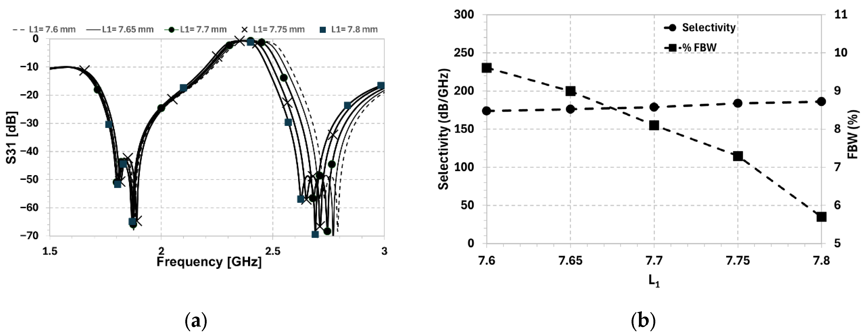
4.2. DGS: FBW Control

The lengths (L1s) of the loading DGSs are made to vary by about ±2.5% (from 7.6 mm to 7.8 mm) with respect to the previously optimized value of 7.7 mm. This length variation will allow control of the passband of the crossover. Figure 13a shows that as L1 increases, the zeros created by the DGS shift towards lower frequencies, while fz1, fz2, and fz4 remain almost unchanged. This effectively helps control the band. Figure 13b shows the upper rejection band selectivity (in dB/GHz) and the Fractional Bandwidths (FBWs) for all the L1 values. In contrast to the previous case, where Lstub was varied, the selectivity remains almost constant and the bandpass changes effectively. The change in the selectivity is ±3.3% around the nominal case (L1 = 7.7 mm). On the other hand, the FBW changes by more than ±24%. Thus, the bandpass and the selectivity of the modified crossover can be controlled easily by only changing a single dimension at a time.

5. Results

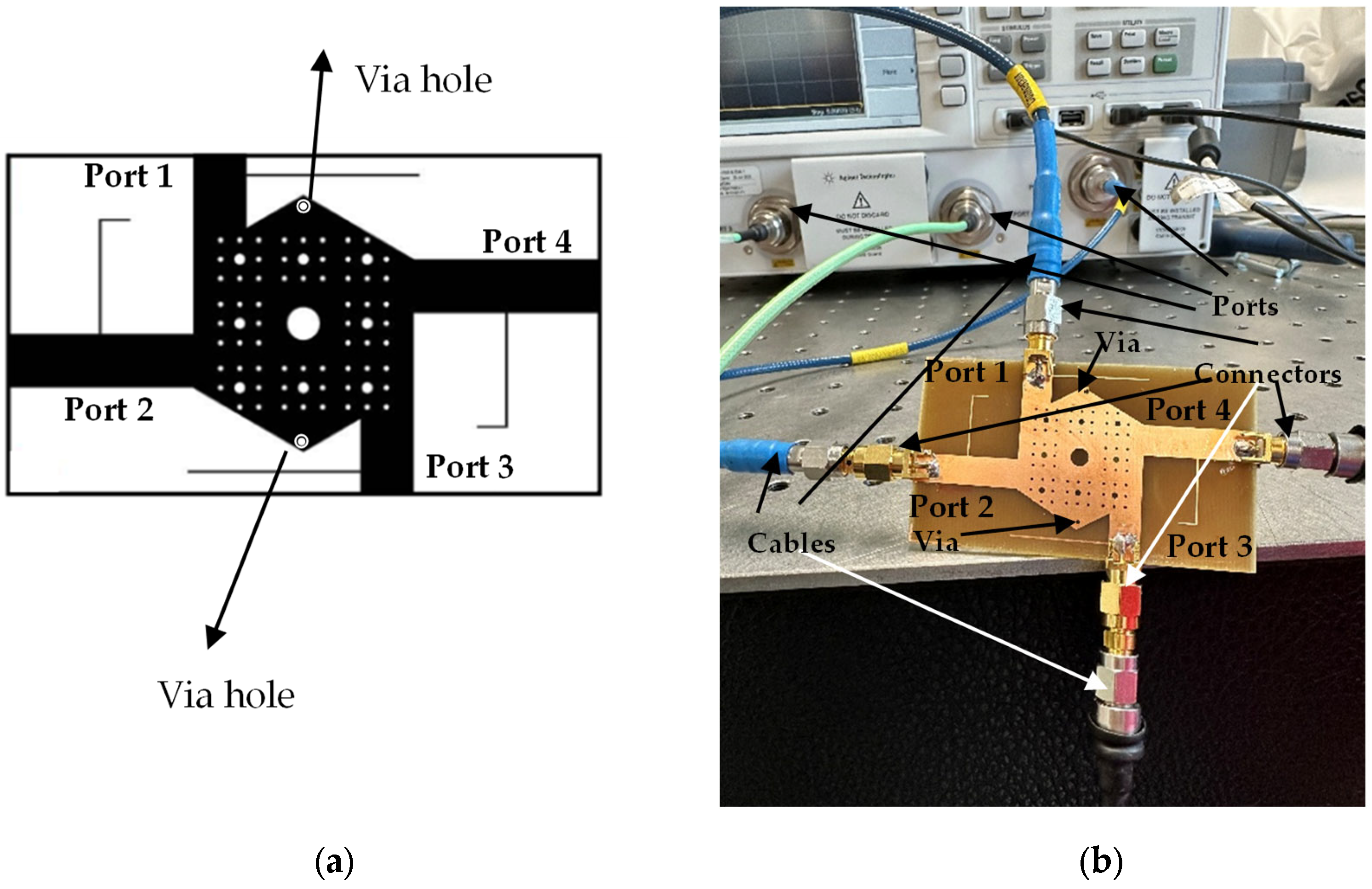
The modified crossover is fabricated and measured using a four-port network analyzer N5222A by Agilent Technologies. Figure 14a shows the final layout of the crossover coupler and Figure 14b shows the fabricated device under measurement. The measurement results for the modified crossover are shown in Figure 15. The calibration method used is the SOLT (Short-Open-Load-Thru) technique, which is the most suitable method for de-embedding the effects of the test fixtures and cables in this four-port microstrip configuration.
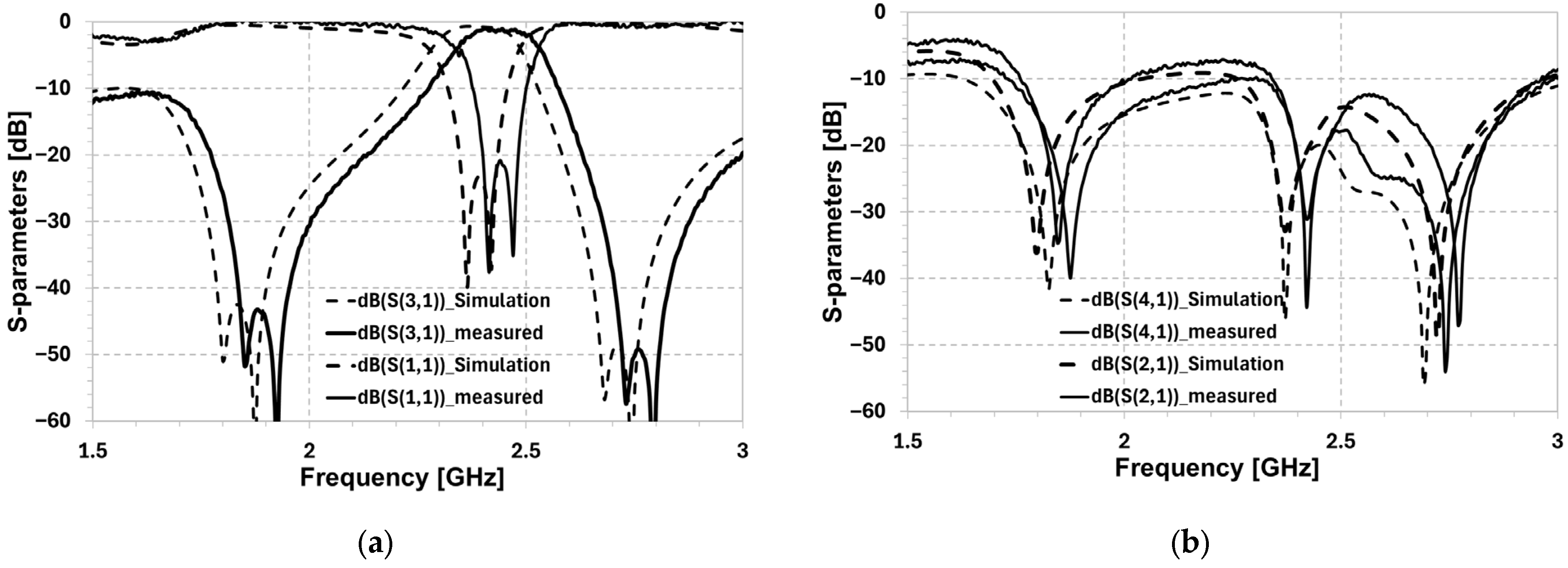
As shown in Figure 15, the measurements validate the proposed design. The response shows good matching and selectivity at the lower and higher bands. Moreover, the insertion loss at 2.4 GHz is about 1 dB (0.7 dB in simulation). In addition, the isolation and matching are better than 17 dB around the operating frequency (25 dB in simulation). The crossover is matched to better than 20 dB (25 dB in simulation). The selectivity at the lower and higher rejection sides of the bandpass is high due to four transmission zeros (two in the lower rejection band and two in the upper one). At fz1 = 1.85 and fz2 = 1.92 GHz, the stubs introduce transmission zeros that prevent signal transmission to port 3. On the other hand, the zero introduced by the DGS occurs at fz3 = 2.79 GHz, as shown in Figure 15.
Compared to simulation results (Figure 11), a frequency shift of less than 50 MHz is obtained. Moreover, the increase in insertion loss obtained in measurements is probably due to some radiation losses and the decrease in matching values. The frequency shift could be due to fabrication tolerances, especially since the design has small gaps.

6. Discussion

To validate the high performance and relevance of the proposed compact hexagonal crossover, its key metrics are benchmarked against contemporary designs published in the literature [14,17,18,19,20,21,22,23,24,25] (Table 3). The comparison focuses on the critical trade-offs between electrical performance (Insertion Loss and Isolation), size, structural complexity, and the crucial feature of Tunability. Complexity is assessed based on fabrication demands (e.g., coupled lines, SIW technology, or multi-layer structures), and Tunability indicates the ability to adjust the frequency response.
The following parameters are used for comparison:
  • fc (GHz): Center frequency.
  • FBW (%): Fractional Bandwidth, calculated at the −3 dB insertion loss level.
  • IL (dB): Insertion Loss (S31), measured at fc.
  • Iso. (dB): Isolation, measured at fc (min (|S21|, |S41|)).
  • RL (dB): Return Loss (S11), measured at fc.
  • Size (mm2): Total footprint area.
  • Complex.: The complexity. A qualitative assessment of fabrication difficulty (+ = complex, ++ = highly complex, e.g., SIW).
  • Selectiv.: The Selectivity. A qualitative measure based on the number and proximity of transmission zeros to the passband (High, Moderate, and Low).
  • Tunab.: The Tunability. A Binary indicator of frequency response adjustment capability (Yes/No).
The data confirms that the proposed design achieves an exceptional balance that few existing studies have matched.
The achieved measured Insertion Loss of 1 dB and Isolation of 25 dB at 2.4 GHz places the design among high-performing planar solutions. While some studies report lower losses (e.g., 0.5 dB in [17,22,25]), they often achieve this by prioritizing simplicity and sacrificing key features, designs [14,19,24] maintain simple, low-loss planar structures but exhibit low Selectivity and no Tunability. In contrast, the proposed design integrates high selectivity (four transmission zeros) alongside low loss, a combination that typically forces designs toward higher complexity and loss (e.g., the 1.8 dB loss in the highly selective design [26]).
The designs in [18,20], rated as ‘+’ (Complex), successfully use minimal complexity to achieve competitive miniaturization. Their footprints are on par with, or smaller than, many of the simple planar designs, while offering superior functionality. Ref. [21] uses Substrate Integrated Waveguide (SIW) technology, which is classified as relatively complex technology due to its requirement for multi-layer fabrication and precise via arrays, significantly increasing manufacturing cost and complexity compared to standard microstrips.
This design’s greatest advantage lies in its unique combination of high Selectivity and Tunability, a feature shared by only a handful of other designs [19,21]. The ability to independently control both the Selectivity (via stubs) and the Fractional Bandwidth (FBW) (via DGS) is a significant technical contribution. The only other highly tunable design [21] achieves its tunability at the cost of significantly higher complexity and a substantially larger footprint. Ultimately, the proposed hexagonal crossover provides an optimal, highly adaptable solution for 2.4 GHz wireless systems, delivering competitive loss and isolation metrics while offering a level of response tunability and selectivity that surpasses most compact, planar counterparts.

7. Conclusions

This study successfully designed and fabricated a novel compact hexagonal microstrip crossover for 2.4 GHz applications. By integrating a Defected Ground Structure (DGS) with reactive loading stubs, the structure achieves an exceptional miniaturization ratio of 62% while maintaining high signal integrity. Crucially, the prototype demonstrated a low Insertion Loss of 1 dB and Isolation better than 20 dB. The key innovation—the independent tunability of the response, allowing the DGS to control the Fractional Bandwidth and the stubs to control Selectivity—was validated. This unique combination of compactness, high performance, and frequency agility establishes the proposed crossover as a highly competitive and adaptable component for modern integrated wireless systems.

Author Contributions

D.K.: Conceptualization; Methodology; Validation (Measurement Setup and Execution); Visualization; Review and Editing. H.I.: Conceptualization; Project Administration; Investigation (Simulation and Optimization); Data Analysis and Interpretation; Writing—Original Draft Preparation; Visualization. All authors have read and agreed to the published version of the manuscript.

Funding

This research received no external funding.

Data Availability Statement

The original contributions presented in this study are included in the article. Further inquiries can be directed to the corresponding author(s).

Conflicts of Interest

The authors declare no conflict of interest.

References

  1. Yerli, M.; Palandöken, M. A compact microstrip Planar crossover for LTE applications. Int. J. Adv. Nat. Sci. Eng. Res. 2023, 7, 473–476. [Google Scholar] [CrossRef]
  2. Singh, A.K.; Kumar, P.; Ray, K.P.; Padhy, B.B. High Performance Low Cost Square Microstrip Crossovers. In Proceedings of the 2025 IEEE Wireless Antenna and Microwave Symposium (WAMS), Chennai, India, 5–8 June 2025. [Google Scholar]
  3. Liu, W.; Zhang, Z.; Feng, Z.; Iskander, M.F. A compact wideband microstrip crossover. IEEE Microw. Wirel. Compon. Lett. 2012, 22, 254–256. [Google Scholar] [CrossRef]
  4. Pang, Y.-H.; Lin, E.D.; Chen, Y.-Y. A Planar balanced crossover. IEEE Trans. Microw. Theory Tech. 2016, 64, 1812–1821. [Google Scholar] [CrossRef]
  5. Chiou, Y.-C.; Lai, S.-W.; Kuo, J.-T. Analysis and design of double-ring crossover junction with arbitrary diagonal port impedances. In Proceedings of the 2009 Asia Pacific Microwave Conference, Singapore, 7–10 December 2009. [Google Scholar]
  6. Pang, Y.-H.; Li, J.-J. A Planar Wideband Balanced Crossover. IEEE Trans. Compon. Packag. Manuf. Technol. 2018, 8, 1807–1814. [Google Scholar] [CrossRef]
  7. Yerli, M.; Palandöken, M. Γ shaped slotted compact circular crossover for communication applications at 2.45 GHz. Int. J. Adv. Nat. Sci. Eng. Res. 2023, 7, 115–119. [Google Scholar] [CrossRef]
  8. Henin, B.; Abbosh, A. Wideband planar microstrip crossover with high power handling capability and low distortion. Microw. Opt. Technol. Lett. 2012, 55, 439–443. [Google Scholar] [CrossRef]
  9. Banat, M.A.; Dib, N.I. Design of miniaturized patch crossover based on superformula slot shapes. Int. J. Electr. Comput. Eng. 2022, 12, 5145–5152. [Google Scholar] [CrossRef]
  10. Nachouane, H.; Najid, A.; Tribak, A.; Riouch, F. Broadband 4 × 4 Butler matrix using wideband 90 hybrid couplers and crossovers for beamforming networks. In Proceedings of the 2014 International Conference on Multimedia Computing and Systems (ICMCS), Marrakech, Morocco, 14–16 April 2014. [Google Scholar]
  11. Yao, B.; Zhang, G.; Zhou, X.; Li, N.; Tang, W.; Yang, J. Substrate-Integrated Waveguide Filtering Crossover Based on 3-D Assembly. IEEE Microw. Wirel. Technol. Lett. 2023, 33, 523–526. [Google Scholar] [CrossRef]
  12. Lal, P.R.; Warrier, P.M.; Menon, S.K. Substrate Integrated Waveguide Based 4-Port Crossover for Beam-Forming Applications. In Proceedings of the Information Systems Design and Intelligent Applications, Visakhapatnam, India, 8–9 January 2016. [Google Scholar]
  13. Tan, X.; Wang, Z.; Zhao, S.; Liu, H.; Gao, M.; Fang, S. A novel Balanced-to-Balanced filtering crossover with wideband isolation and Common-Mode suppression. Microw. Opt. Technol. Lett. 2024, 66, e70044. [Google Scholar] [CrossRef]
  14. Purnima, G.; Menon, S.K. Microstrip patch based high isolation planar crossover for beamforming applications. In Proceedings of the 2016 IEEE International WIE Conference on Electrical and Computer Engineering (WIECON-ECE), Pune, India, 19–21 December 2016. [Google Scholar]
  15. Akra, M.; Issa, H.; Pistono, E.; Jrad, A.; Corrao, N.; Ferrari, P. Parallel-coupled Stub-loaded Resonator filters with wide spurious suppression. In Proceedings of the 2012 42nd European Microwave Conference, Amsterdam, The Netherlands, 29 October–1 November 2012. [Google Scholar]
  16. Mohammed, W.; Philippe, F.; Cedric, D. mm-wave Dual-Mode Grounded Microstrip Patch BandPass Filter on 55-nm BiCMOS. In Proceedings of the 2021 IEEE MTT-S International Microwave Filter Workshop (IMFW), Perugia, Italy, 17–19 November 2021. [Google Scholar]
  17. Zhu, H.; Wang, Y.; Abbosh, A.M. Broadband microwave crossover using parallel-coupled microstrip lines and short-ended stubs. IET Microw. Antennas Propag. 2014, 9, 79–85. [Google Scholar] [CrossRef]
  18. Wu, Q.; Zhao, X.; Liu, X.; Shi, X. Analysis and design of compact planar crossover. In Proceedings of the 2015 Asia-Pacific Microwave Conference (APMC), Nanjing, China, 6–9 December 2015. [Google Scholar]
  19. Guo, Q.-Y.; Zhang, X.Y.; Gao, L. Novel Compact Planar Crossover With Bandpass Response Based on Cross-Shaped Resonator. IEEE Trans. Compon. Packag. Manuf. Technol. 2017, 7, 2018–2026. [Google Scholar] [CrossRef]
  20. Zhang, S.; Sun, S. Modified window shape-based crossover with enhanced bandwidth. Int. J. RF Microw. Comput.-Aided Eng. 2020, 31, e22503. [Google Scholar] [CrossRef]
  21. Karthikeyan, S.S. Compact dual-band substrate integrated waveguide crossover with high isolation. Prog. Electromagn. Res. Lett. 2019, 83, 23–28. [Google Scholar] [CrossRef]
  22. Kim, T.; Choi, J. Miniaturized multi-section crossover with open stub. In Proceedings of the 2015 IEEE International Symposium on Antennas and Propagation & USNC/URSI National Radio Science Meeting, Vancouver, BC, Canada, 19–24 July 2015. [Google Scholar]
  23. Lee, Z.-w.; Pang, Y.-h. Compact planar dual-band crossover using two-section branch-line coupler. Electron. Lett. 2012, 48, 1348–1349. [Google Scholar] [CrossRef]
  24. Krishna, I.S.; Barik, R.K.; Karthikeyan, S.S. Analysis and Design of a Planar Crossover for Dual-Frequency Applications. In Proceedings of the 2017 14th IEEE India Council International Conference (INDICON), Roorkee, India, 15–17 December 2017. [Google Scholar]
  25. Singh, A.K.; Kumar, P.; Ray, K.P.; Padhy, B.B. Miniaturized Circular Slotted Crossovers with Defected Ground Structures. In Proceedings of the 2024 IEEE Microwaves, Antennas, and Propagation Conference (MAPCON), Hyderabad, India, 9–13 December 2024. [Google Scholar]
  26. Shao, Q.; Yang, N.; Chen, R.-S.; Huang, G.-L.; Chen, F.-C.; Wang, Y. Design of Filtering Crossover Based on 180 Filtering Couplers. IEEE Trans. Compon. Packag. Manuf. Technol. 2024, 14, 309–314. [Google Scholar] [CrossRef]
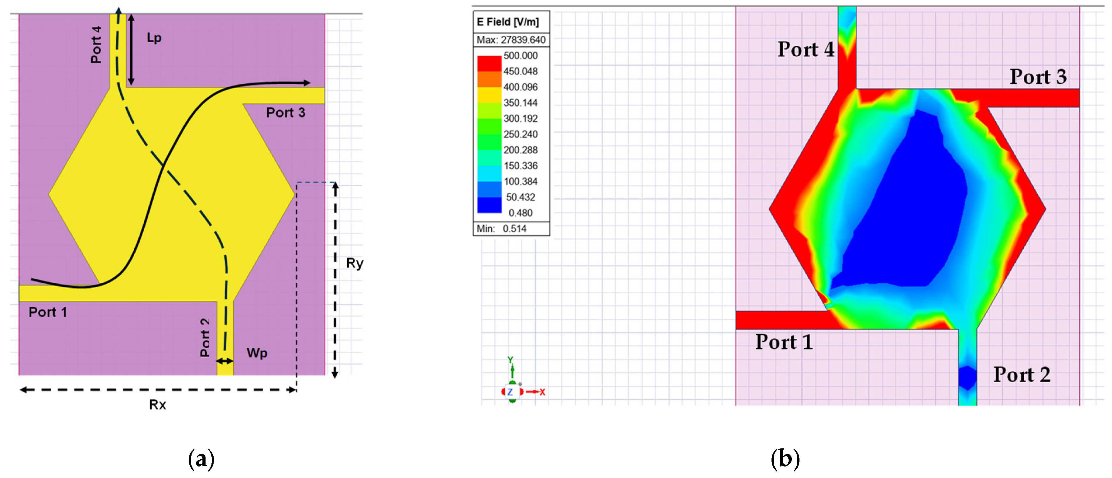
Figure 1. Classical hexagonal crossover. (a) Topology and (b) electric field intensity plot at 2.4 GHz when the input is at port 1.
Electronics 14 04737 g001
Figure 2. S-parameter response of the classical hexagonal crossover.
Electronics 14 04737 g002
Figure 3. Compact hexagonal crossover with Sierpinski carpets and DGSs: (a) topology and (b) electric field intensity plot at 2.4 GHz when the input is at port 1.
Electronics 14 04737 g003
Figure 4. S-parameter response of the classical hexagonal crossover.
Electronics 14 04737 g004
Figure 5. Compact hexagonal crossover with Sierpinski carpets and DGSs: (a) topology and (b) electric field intensity plot at 2.9 GHz when the input is at port 1.
Electronics 14 04737 g005
Figure 6. (a) Phase imbalance (PI) and (b) amplitude imbalance (AI) for the compact and classical crossovers.
Electronics 14 04737 g006
Figure 7. EF distribution at 1.9 GHz.
Electronics 14 04737 g007
Figure 8. (a) The Designed crossover, and (b) Gap introduced at the ports to study the excited modes of the crossover.
Electronics 14 04737 g008
Figure 9. Excited modes with and without via holes.
Electronics 14 04737 g009
Figure 10. The modified compact hexagonal crossover: (a) The design. (b) The EF intensity at 2.4 GHz, (c) at 1.81 GHz, (d) at 1.89 GHz, and (e) at 2.75 GHz.
Electronics 14 04737 g010
Figure 11. S-parameter response of the modified hexagonal crossover.
Electronics 14 04737 g011
Figure 12. Lstub1 variation by ±33.3%. (a) Transmission coefficient. (b) Selectivity and FBW.
Electronics 14 04737 g012
Figure 13. L1 variation by ±2.5%. (a) Transmission. (b) Selectivity and FBW variations.
Electronics 14 04737 g013
Figure 14. (a) Layout of the crossover coupler and (b) device under measurement.
Electronics 14 04737 g014
Figure 15. Measurement and simulation results: (a) transmission and reflection coefficients and (b) isolation coefficients.
Electronics 14 04737 g015
Table 1. Dimensions in mm of the compact crossover.
RxRyD1L1W1S1S2S3WpLp
25262.67.51.450.250.1250.3752.758.4
Table 2. Dimensions in mm of the compact crossover.
RxRyD1L1L2S1Lstub1Lstub2Lstub3,4dvWstubWpLp
28292.67.73.850.152423.7518.50.80.7567.3
Table 3. Comparison with state-of-the-art.
Ref.Fc
(GHz)
FBW
(%)
IL
(dB)
Iso.
(dB)
RL
(dB)
Size (mm2)Complex.Selectiv.Tunab.
[14]2.412.50.553528253-lowno
[17]2.412.50.5152231 × 31-lowno
[18]2.4250.5201539.4 × 27+lowno
[19]2.44.41.46232021.6 × 31.6+highyes
[20]2.4401151550 × 50+moderateno
[21]2.410.91402043.2 × 43.2++lowyes
[22]2.5220.5202029.3 × 9.3-lowno
[23]2.43.351.35203060.3 × 48.9-highno
[24]2.43.750.88302032.4 × 37.2-lowno
[25]2.59.350.58253035.5 × 35.5-lowno
[26]2.4101.8151090 × 45-highno
our work2.42.28–2.51252533 × 58-highyes
Disclaimer/Publisher’s Note: The statements, opinions and data contained in all publications are solely those of the individual author(s) and contributor(s) and not of MDPI and/or the editor(s). MDPI and/or the editor(s) disclaim responsibility for any injury to people or property resulting from any ideas, methods, instructions or products referred to in the content.