1. Introduction
The Internet of Things (IoT) is a rapidly evolving technology that has the potential to disrupt multiple sectors, with an estimated 29 billion connected devices by 2030 [
1]. However, this proliferation of connected devices and the vast amount of data they generate also poses significant challenges in terms of security and privacy. The interconnected nature of the IoT makes it vulnerable to malicious attacks, such as Distributed Denial of Service (DDoS) attacks [
2], and other cyber threats, including phishing attacks, man-in-the-middle attacks, and IP spoofing attacks [
3], which can have serious consequences.
It is crucial to address these concerns and ensure the secure and effective deployment of IoT devices. This includes implementing security measures that can accommodate the wide range of computational capabilities of IoT devices, from low-power sensors to high-performance edge servers. These measures should also take into account the physical accessibility of the devices, as this can greatly influence attack surfaces [
4]. Furthermore, IoT security solutions should be both scalable and cost-effective. Therefore, conventional cryptographic methods, while effective in securing data and protecting privacy, can present challenges when applied to IoT applications [
5,
6]. These methods often require complex computations that can be demanding in terms of power consumption, making them unsuitable for devices with limited computational capabilities or energy constraints. High power requirements of these approaches can also result in devices with a larger form factor, which is often prohibitively expensive. This highlights the need for alternative, lightweight and power-efficient security solutions that can be easily integrated into IoT devices and networks. One promising approach is the use of Physical Unclonable Functions (PUFs). PUFs are hardware-based security primitives unique to every device and are not stored in any external memory; therefore, they cannot be extracted or cloned. They essentially use variations in the manufacturing process to create unique digital fingerprints for the corresponding electronic devices. PUFs produce these unique, unpredictable random responses
R from input challenges
C represented as challenge–response pairs (CRPs); thus, each IoT device can produce unique responses from the same challenges. PUFs generally consume less power, are small in size and easy to implement, and provide physical security for IoT systems.
PUF can be divided into two categories based on the relationship between the number of CRPs: weak PUF and strong PUF. Strong PUFs provide a large number of CRPs, which can be utilized for authentication. However, weak PUFs have a limited number of CRPs that are usually used for key generations. One of the most common strong PUFs is Arbiter PUF (APUF) [
4], which contrasts delays when applying challenges on two paths of multiplexers (usually interconnected upper and lower routes), which generates a response bit of ‘0’ or ‘1’ based on which route is faster, as determined by a flip-flop acting as an arbiter. However, APUFs suffer from poor uniqueness due to the difficulty of achieving balance and uniformity of the routing paths on the hardware chip. Another type of PUFs is Ring Oscillator PUF (RO PUF) [
7], which is based on the principle of the oscillation period of a ring oscillator circuit, making it suitable to be implemented on a Field-Programmable Gate Array (FPGA) due to its low routing stress compared to APUF. However, one of the trade-offs of using an RO PUF is that it generates fewer response bits than other PUF designs. Therefore, to generate the same number of CRPs as an APUF, an RO PUF would require more area on the device [
8], which is usually expensive. In contrast, weak PUFs, including memory-based, rely on the initial powering up of memory cells to generate random responses, such as Static Random Access Memory (SRAM) PUF [
9,
10] and Butterfly PUF [
11].
While PUF has been implemented on Application-Specific Integrated Circuits (ASICs), the most common PUF implementation platform is an FPGA. FPGAs are rapidly becoming popular in various applications, from smart city infrastructure to data center acceleration, due to their flexibility, high density of logic, and shorter time-to-market [
12]. However, developing an efficient and lightweight security approach that is suitable for low-cost FPGA-based IoT applications remains an open challenge in this field, which is what we attempt to do in this paper.
In this paper, we propose a lightweight, strong PUF based on an FPGA to generate large CRPs suitable for authentication. The main advantages of our proposal can be summarized as follows:
The proposed Linear Feedback Shift Register PUF (LFSR-PUF) can generate multiple responses for the same challenge using configurable primitive feedback on the LFSR structure.
The design is flexible and can operate in different modes with various CRPs.
The proposed design utilized small hardware overhead and power consumption, making it scalable for lightweight applications.
The rest of this paper is organized as follows:
Section 2 reviews related work on LFSR-based PUFs, including prior FPGA implementations and their limitations.
Section 3 presents the proposed delay-based configurable LFSR-PUF design, with emphasis on architecture and design considerations. The FPGA implementation details, including architecture and resource utilization, are provided in
Section 4.
Section 5 evaluates the performance of our design, covering uniformity, uniqueness, statistical test results, and comparison with related PUFs.
Section 6 discusses the resilience of the proposed PUF against classical and deep learning modeling attacks.
Section 7 provides an in-depth analysis of implementation trade-offs, CRP scalability, and potential directions for extending the design. Finally,
Section 8 concludes the paper with key findings and outlines directions for future work.
3. Proposed PUF Design
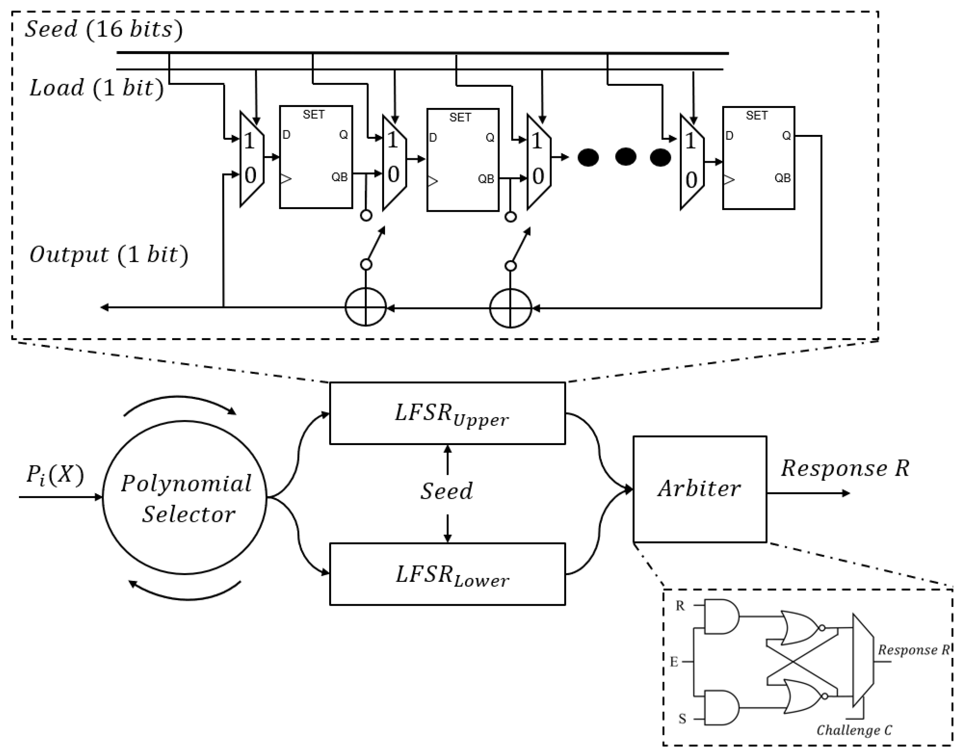
Our proposed PUF is a state-of-the-art, delay-based PUF that utilizes the inherent physical variations in the internal elements of a configurable Fibonacci (The term “Fibonacci LFSR” refers to a type of linear feedback shift register where the feedback mechanism relies on XORing non-adjacent stages of the shift register. This type of LFSR is commonly used in various digital applications for generating pseudo-random sequences.) LFSR circuit to generate a unique output. The design, illustrated in
Figure 1, capitalizes on the intrinsic variations in delay between different paths in the LFSR circuit, which are an inevitable outcome of the manufacturing process. An arbiter at the end of the LFSR selects between paths based on the challenge values. The output is highly dependent on the physical characteristics of the circuit components, physical routing, and placements in the FPGA, making it difficult to replicate or predict.
The fundamental building blocks of an LFSR are flip-flops. They can store one bit of information, “0” or “1”, and change state (flip) in response to a clock signal. In each clock cycle, the contents of the register are shifted by one position. This is typically done by feeding the output of each flip-flop into the input of the next one in the chain, which is combined with XOR gates. The XOR gates receive inputs from the feedback taps and the
output of the flip-flop. The switch connects the
output to the XOR gate, properly configuring the feedback path according to the selected primitive polynomial. The outputs of the two LFSR delay paths are connected to the SR-latch as follows: the upper LFSR output drives the Reset
R input, and the lower LFSR output drives the Set
S input. The use of flip-flops as coarse-grain delay elements in the design can introduce variability in signal propagation, resulting in potential race conditions among the flip-flops for both LFSRs. The LFSR flip-flops are first
RESET and then triggered by a
START signal at the rising edge that is controlled through the FPGA switches with the initialization input random seeds using the load signal. This signal is required only during initialization to synchronize the start of both LFSRs. All flip-flops in each LFSR are driven by the same global FPGA clock signal, ensuring that every stage updates synchronously. Each LFSR is implemented as a 16-bit register, so its internal state, feedback paths, and seed inputs are 16-bit buses. In contrast, the challenge input
C, enable signal
E, and the arbiter Set
S, Reset
R, and output lines are single-bit connections. The challenge is applied bit by bit per clock cycle, and the arbiter produces a 1-bit response. The polynomial selectors
play a crucial role in this process as they select the feedback polynomials and determine the primitive feedback for both LFSRs. A possible utilization of these feedback polynomials used in this design is listed in
Table 1. There are 2048 possible primitive polynomial equations of degree 16 that can be used for the LFSR [
24]. However, the polynomial selector dynamically updates the feedback polynomial equations based on the user selection through the FPGA switches, allowing for specific shift cycle operation.
Moreover, the responses
R are generated by an arbitration circuit composed of an enable SR-latch and an integrated 2:1 multiplexer (MUX) driven by the applied challenge
C. In our design, the role of the multiplexer is not to perform post hoc output selection but to introduce a configurable, challenge-dependent switching effect that influences the effective delay path leading to arbiter resolution. The SR-latch resolves the timing difference caused by the physical delay variations in the dual LFSR paths, and the MUX ensures that each challenge dynamically interacts with these variations during arbitration. The possibility of both LFSR outputs evaluating to zero is extremely rare, since entropy originates from physical delay mismatches among flip-flops and routing paths. This configuration maintains the challenge application within the arbitration process itself, ensuring that the response behavior reflects physical delay variability rather than deterministic logic. To preserve strong PUF behavior, the configuration index of the selected primitive feedback polynomial can be treated as part of the challenge vector
, because only the user knows the index selected, i.e.,
where
i identifies the active polynomial
. Hence, every combination of input challenge bits and polynomial index corresponds to a unique CRP. Furthermore, we consider the randomness strength and hardware overhead of choosing the LFSR length. The LFSR can be scaled to 32, 64 or 128 bits for our design. The period of an LFSR is determined by its feedback connections and the number of flip-flops used, so the circuit can run for the full period, which is the maximum length of the n-bit LFSR
, for each feedback polynomial and update before the sequence repetition. For each selected primitive feedback, 65,535 bits are generated.
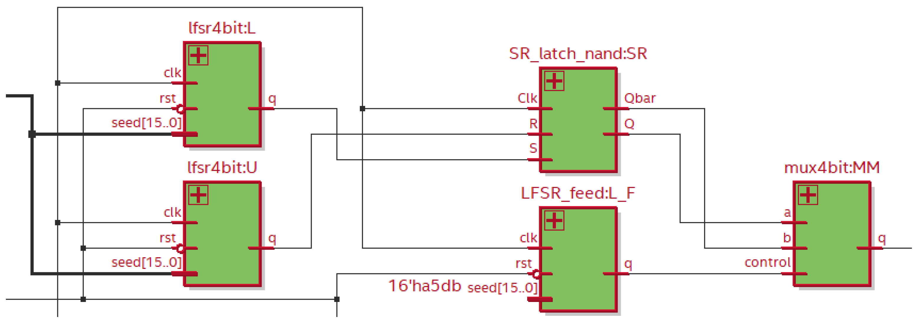
Figure 2 illustrates the Register Transfer Level (RTL), which represents the hardware description at a level of abstraction that describes how data is transferred between registers and components.
4. FPGA Implementation
In this work, we implemented our PUF on the Altera Cyclone IV DE2-115 4CE115 FPGA development board. The architecture of the cyclone IV 60nm FPGA consists of the basic LABs, each comprising groups of LEs, which are the smallest units in the device, with a total of 114,480 LEs in the FPGA. Each LAB is composed of 16 LEs, LAB control-signals, LE carry-chains, register-chains and local interconnect. The local interconnect transfers signals between LEs in the same LAB, while the register chain connections transfer the output of one LE register to the adjacent LE register in a LAB [
25]. We used Quartus Prime 20.1 Lite Edition to implement our PUF. The compiler places associated design elements in a LAB based on the performance and area efficiency. However, this introduces a bias due to the physical placement and routing mismatch, especially in the delay-based PUF. Therefore, the compiler settings were carefully adjusted to manage routing variability, which is critical in delay-based PUFs:
Location constraints: These were specified in the Quartus Settings File (QSF) to ensure that symmetric paths in the LFSR were placed adjacent. Without such constraints, Quartus optimization may unbalance routing paths and degrade uniqueness.
Manual LUT: The routing is balanced manually through the Lookup Table (LUT) inputs.
The routing and placement of the design logic elements within the FPGA can greatly impact the performance metrics, particularly in terms of uniqueness. When the design is left to the automated synthesis and routing of the Quartus tool, it results in identical CRPs and no observable uniqueness. Therefore, the uniqueness and unpredictability of our PUF arise only when routing is preserved, confirming the physical entropy source of the proposed design. The challenge–response pairs are exchanged between a PC and the FPGA through the RS-232 serial communication interface. The experimental results were then recorded and further processed using MATLAB version R2024b.
A primary advantage of our proposed PUF is that it requires low hardware overhead compared to most existing designs, which usually combine LFSR techniques with weak PUF. The proposed PUF utilized 32 LEs in total for both upper and lower LFSRs, each flip-flop with a related MUX implemented on one LE. The arbiter at the final stage was implemented in two adjacent LABs. The total resource utilization reported in
Table 2 (291 LEs) includes the peripheral control circuits required, whereas the core PUF logic itself occupies only 41 LEs, including the SR-latch. The performance and logic utilization of different types of FPGAs can vary based on the manufacturing techniques of the chip.
Table 2 summarizes the total FPGA utilization resources of the design, including peripheral circuits, such as circuits used for the serial communication interface. Furthermore, the total thermal power dissipation reported by Quartus using a power analyzer tool is 130.06 mW, which is the estimated total power dissipation result for the design with the peripheral circuit.
The experimental results show that the LFSR-PUF design in this paper has a very small hardware overhead and is suitable for lightweight devices.
6. Security Evaluation
To be considered a strong PUF, a design must have a large CRP space. However, attackers can train machine learning algorithms on known CRPs to predict unknown responses. To counteract this, a PUF design must increase the randomness of the CRP space and reduce the correlation between CRPs. A commonly used method to generate random numbers is LFSR, but the sequences generated directly by LFSR are not cryptographically secure and can be easily determined by analyzing their sequence using, for example, the Berlekamp-Massey algorithm. As demonstrated in
Section 3, our proposed PUF is not directly dependent on the LFSR; rather, it is a delay-based PUF that utilizes the inherent physical variations in the internal elements of a configurable LFSR circuit to provide high randomness in the CRP space and reduce the correlation between them.
Machine learning-based modeling attacks have recently become common, making ML attack resistance a key security measure for PUFs [
16,
17,
18]. In a typical ML attack, the attacker performs a man-in-the-middle (MITM) attack, where they intercept the communication between the device and the server without having physical access to the device. The attacker then collects and records CRPs, and applies the ML attack to predict and learn the correlation between CRPs, allowing them to gain unauthorized access to the device and its sensitive data.
To assess the robustness of our design, we tested the resistance of our proposed PUF against the ML modeling attack using some common classical ML algorithms (Logistic Regression (LR), Support Vector Machine (SVM), Random Forest Classifier (RF)) and Deep Learning (DL) algorithms (Multi-layer Perceptron (MLP), Convolutional Neural Networks (CNN), Recurrent Neural Networks (RNN)). We generated 327,675 CRPs from our PUF and divided them into 80% training CRPs and 20% testing CRPs. This dataset size is comparable to those used in several recent studies on delay-based LFSR PUFs, as shown in
Table 4. This scale is generally considered sufficient to capture potential CRP correlations if they exist. The hyperparameter values we used in the experiments with the classical ML algorithms are listed in
Table 5. Similarly, the structures of DL algorithms are provided in
Table 6.
A description of the structures used for deep neural networks (CNN and RNN with Long Short-Term Memory (LSTM)) is given in
Table 7; for the SVM, LR, RF, and MLP models, we used Python’s scikit-learn library.
We used the binary classification approach for the ML attacks experiments based on the generated CRP binary dataset. As part of preprocessing, the challenges and responses of the CRP dataset are converted into one-dimensional vectors of binaries. The challenges vector’s elements indicate a particular feature, while the responses vector represents a binary value of 1 or 0.
We conducted the training by feeding the dataset to the models and reshaping it as required.
Table 8 shows our results, where the accuracy of predictions is almost equivalent to random guesses of 50% for all the ML/DL algorithms. Similarly, the precision achieved does not show a clear growth trend among the training dataset.
Our design has the unique capability of producing a large number of CRPs without relying on the combination methods, thereby reducing computational overhead. This not only results in a smaller PUF circuit but also enhances resistance to ML/DL attacks. Our design is a significant improvement over previous work in this area, as it allows for key generation at a significantly lower cost. To further illustrate this point, a summary comparison highlighting the resistance to ML attacks between our design and previous work is provided in
Table 9.
7. Discussion
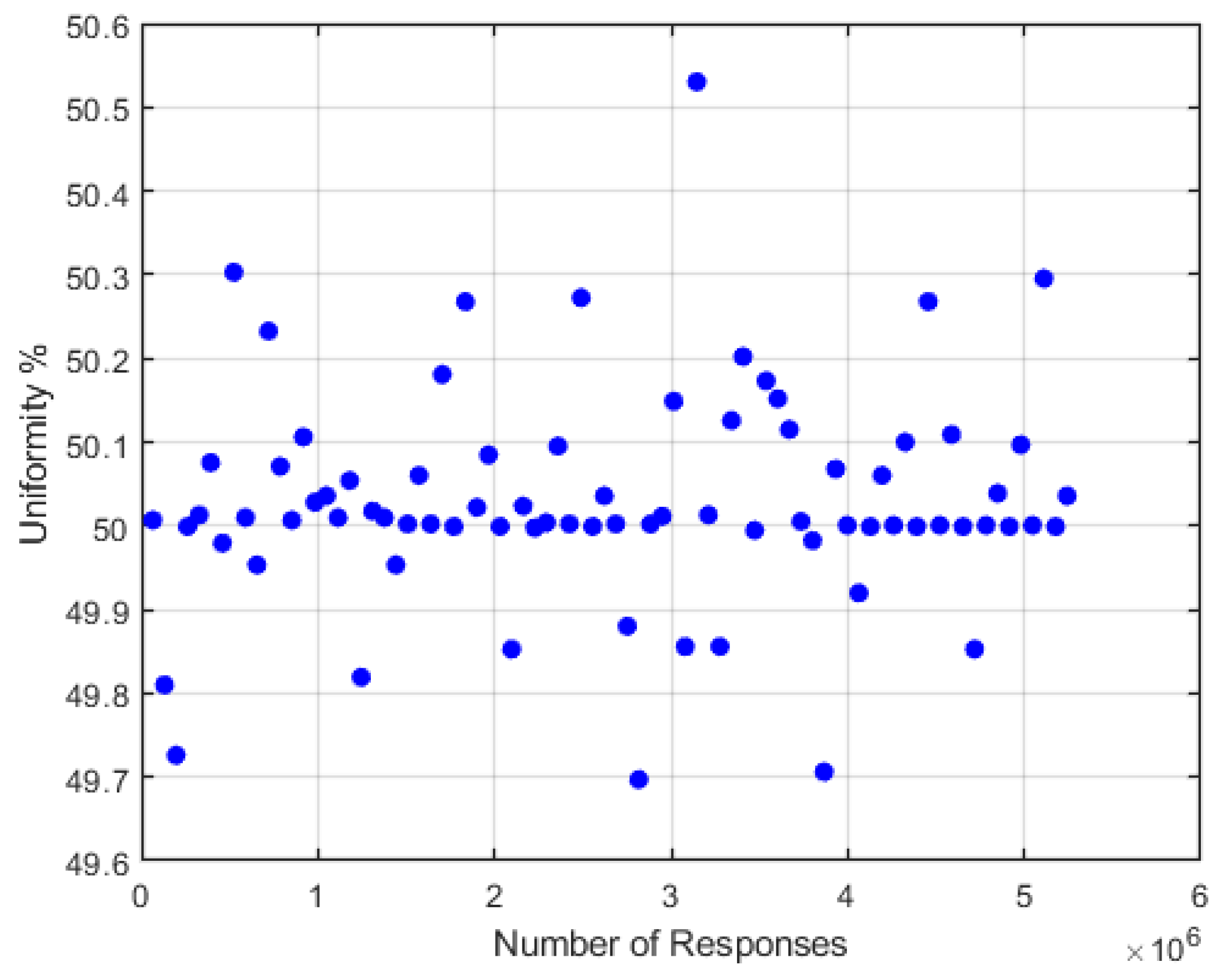
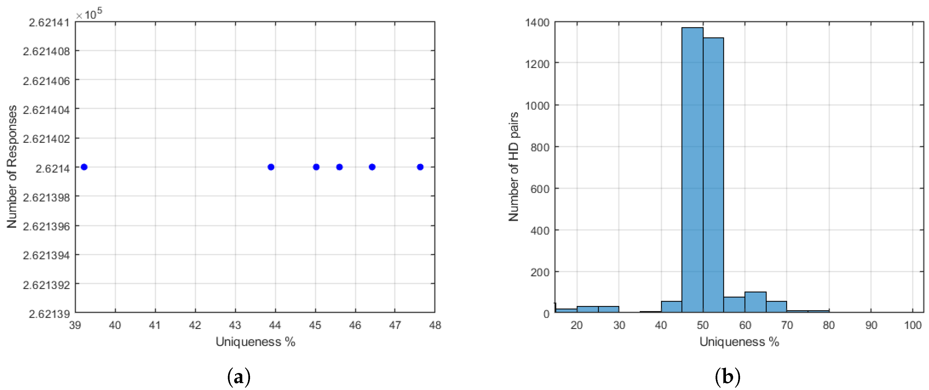
The results of our proposed lightweight configurable LFSR-PUF demonstrate strong potential for deployment in IoT and other resource-constrained environments. Compared with earlier designs that combine weak PUFs with LFSR logic, our approach relies purely on the intrinsic delay variations of a configurable LFSR structure. This leads to a compact design that achieves near-ideal uniformity 50.03% and uniqueness 49.15%, while maintaining very low hardware overhead of less than 1% of FPGA resources and conservative power consumption of 130.06 mW.
One of the key contributions is the ability to generate multiple random responses from the same challenge by dynamically switching between primitive feedback polynomials. This significantly expands the CRPs without introducing additional hardware complexity, making the design particularly suited for authentication protocols in IoT systems. In addition, the scalability of the LFSR length (16, 32, 64, and 128 bits) provides further flexibility depending on the application requirements.
In our design, we selected a 16-bit LFSR-PUF as a practical balance between lightweight implementation and proof-of-concept validation on an FPGA. A 16-bit LFSR already provides a maximum period of
= 65,535 states per primitive polynomial. With
K configurable primitive polynomials, the response capacity of the design can be formally estimated as follows:
For our case (
), this yields approximately 262,140 unique responses per device. In practice, we used 5 groups of challenges, with each group containing 65,535 bits, across 4 different polynomial feedbacks per FPGA, producing a total of 5.2 million response bits. These groups of challenges with their seeds were generated as pseudorandom sequences to ensure diversity and reduce bias in the evaluation. This dataset was sufficient to thoroughly evaluate uniformity, uniqueness, randomness via NIST statistical tests, and resistance to machine learning attacks.
Compared with conventional PUFs, differences in CRP scalability are evident. An
N-stage APUF [
28] provides a nominal CRP space of
. For instance, a 64-stage APUF can generate
CRPs, while a 128-stage APUF can generate
CRPs. Despite this massive capacity, APUFs are highly vulnerable to modeling attacks and require strong countermeasures. By contrast, an RO PUF [
7] with
N oscillators yields
pairwise comparisons, but the number of independent bits is limited to
due to correlations. For example, 35 oscillators produce ≈133 independent bits, 128 oscillators ≈716 bits, and 1024 oscillators ≈8769 bits. While these designs offer very large raw CRP capacities, they require much higher hardware resources and often suffer from routing imbalance or reliability issues.
Our configurable LFSR-PUF achieves predictable and scalable CRP capacity with minimal overhead. Extending to with would yield ≈1.72 × responses per device. Combined with near-ideal performance metrics and strong resistance to ML/DL modeling attacks, this demonstrates that our design represents a practical trade-off: it avoids extreme CRP cardinality, but achieves efficiency, robustness, and scalability, making it well-suited for IoT authentication and security applications.
Our configurable LFSR-PUF achieves scalable CRP capacity with minimal overhead. Extending to with would yield responses per device. Moreover, the architecture offers flexibility by allowing scalability in both the LFSR length n and the number of primitive polynomials K. For instance, even with , increasing K to 6, 7, or 8 would proportionally expand the CRP space, while moving to and larger values of K would further boost the response capacity. Combined with near-ideal performance metrics and strong resistance to ML/DL modeling attacks, this demonstrates that our design represents a practical trade-off between CRP size and implementation efficiency, delivering robustness and scalability that make it particularly suitable for IoT applications.
The security evaluation confirmed that our design is resilient against both classical ML algorithms (SVM, LR, and RF) and DL methods (MLP, CNN, and RNN). Across all cases, prediction accuracy remained close to random guessing at around 50%. This high resistance is primarily achieved due to the delay-based architecture and the reduced correlation between CRPs.
Some challenges and open issues still need to be considered. The current implementation focused on FPGA-based evaluation under controlled operating conditions. Reliability under environmental variations, such as temperature and voltage fluctuations, was not extensively tested, as suitable FPGA testbed environments were not accessible. Long-term effects, including transistor aging, may also influence the stability of the PUF responses. These aspects remain important directions for future research. In addition, recent studies have highlighted emerging hardware and side-channel threats targeting smart devices. The authors in [
29] demonstrated that electromagnetic emanations from in-display fingerprint sensors can be exploited to reconstruct user fingerprints, exposing critical vulnerabilities in embedded biometric systems. Similarly, authors in [
30] analyzed co-located website fingerprinting attacks and revealed that microarchitectural interference between processes can leak sensitive execution patterns. These works underline the increasing sophistication of hardware-based attacks and the necessity of designing secure, unpredictable primitives at the hardware level. Although our work uses the intrinsic hardware process variations as an entropy source in the proposed delay-based LFSR-PUF to reduce susceptibility to cloning and modeling attacks that rely on deterministic circuit behavior.
Overall, the proposed design delivers a balance between low-cost implementation and strong resilience to modeling attacks, outperforming several recent LFSR-based PUF approaches. Wider validation across different hardware platforms and environmental conditions will be required to ensure robustness for real-world deployment.
8. Conclusions and Future Work
In this paper, we propose a lightweight secure delay-based LFSR-PUF design utilizing configurable primitive feedback and inherent physical variations in the internal elements of the circuit. The design has a simple structure, is easily implemented on an FPGA with very small hardware overhead, and is suitable for lightweight applications, such as IoT. Our proposed PUF provides large CRP spaces without combining weak PUF with conventional security, as is the case with most previous work, which greatly improves its efficiency. The experimental evaluation confirmed near-ideal performance with 50.03% uniformity and 49.15% uniqueness, while successfully passing the NIST statistical test suite, validating the quality of the randomness of the responses. The implementation of FPGA also achieved a low power consumption of 130.06 mW, demonstrating practicality for resource-constrained IoT devices. Moreover, security analysis against classical ML algorithms (SVM, LR, and RF) and deep learning models (MLP, CNN, and RNN) showed resistance to modeling attacks, with prediction accuracies close to random guessing ≈50%. These results highlight that the proposed PUF offers a secure and efficient solution for device authentication and key generation in IoT systems. This work can be extended by evaluating the reliability of the design under variations of supply voltage, temperature, and different modes of operation in more FPGA devices (which was not possible due to the lack of suitable FPGA testbeds). In addition, future research should also consider resilience against advanced attack techniques such as reliability-based modeling and side-channel-assisted machine learning, which are emerging threats for PUF designs, as well as implementing the proposed PUF in denser FPGA environments to evaluate the impact of routing congestion and resource utilization on the uniqueness, stability, and overall performance of the design.


